POWER SUPPLY - · PDF fileSimplified diagram of positive power supply 120VAC ... Figure 1...
8
POWER SUPPLY MODEL XP-15 Instruction Manual Copyright © 2013 by Elenco ® Electronics, Inc. REV-A 753020 All rights reserved. No part of this book shall be reproduced by any means; electronic, photocopying, or otherwise without written permission from the publisher. ELENCO ®
Transcript of POWER SUPPLY - · PDF fileSimplified diagram of positive power supply 120VAC ... Figure 1...

POWER SUPPLY
MODEL XP-15
Instruction Manual
Copyright © 2013 by Elenco® Electronics, Inc. REV-A 753020All rights reserved.No part of this book shall be reproduced by any means; electronic, photocopying, or otherwise without written permissionfrom the publisher.
ELENCO®
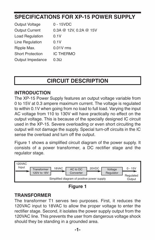
Figure 1
Simplified diagram of positive power supply
120VAC Input 18VAC 20VDC 0 - 15V
RegulatedOutput
Transformer120V to 18V
AC to DCConverter
VoltageRegulator
CIRCUIT DESCRIPTION
INTRODUCTIONThe XP-15 Power Supply features an output voltage variable from0 to 15V at 0.3 ampere maximum current. The voltage is regulatedto within 0.1V when going from no load to full load. Varying the inputAC voltage from 110 to 130V will have practically no effect on theoutput voltage. This is because of the specially designed IC circuitused in the XP-15. Severe overloading or even short circuiting theoutput will not damage the supply. Special turn-off circuits in the ICsense the overload and turn off the output.
Figure 1 shows a simplified circuit diagram of the power supply. Itconsists of a power transformer, a DC rectifier stage and theregulator stage.
-1-
TRANSFORMERThe transformer T1 serves two purposes. First, it reduces the120VAC input to 18VAC to allow the proper voltage to enter therectifier stage. Second, it isolates the power supply output from the120VAC line. This prevents the user from dangerous voltage shockshould they be standing in a grounded area.
SPECIFICATIONS FOR XP-15 POWER SUPPLYOutput Voltage 0 - 15VDC
Output Current 0.3A @ 12V, 0.2A @ 15V
Load Regulation 0.1V
Line Regulation 0.1V
Ripple Max. 0.01V rms
Short Protection IC THERMO
Output Impedance 0.3W

-2-
AC to DC CONVERTER
The AC to DC converter consists ofdiodes D1 and D3 and capacitor C1.Transformer T1 has two secondarywindings which are 180 degrees outof phase. The AC output of eachwinding is shown in Figure 2A and 2B.
Diodes are semiconductor devicesthat allow current to flow in onedirection. The arrow in Figure 3 pointsto the direction that the current willflow. Only when the transformervoltage is positive will current flowthrough the diodes. Figure 3 showsthe simplest possible rectifier circuit.This circuit is known as a half waverectifier. Here, the diode conducts onlyhalf the time when the AC wave ispositive as shown in Figure 2C. Use of thiscircuit is simple but inefficient. The big gapbetween cycles requires much more filtering toobtain a smooth DC voltage.
By the addition of a second diode andtransformer winding, we can fill in the gapbetween cycles as shown in Figure 4. Thiscircuit is called full wave rectification. Eachdiode con-ducts when the voltage is positive.By adding the two outputs, the voltagepresented to capacitor C1 is more complete,thus, easier to filter, as shown in Figure 2F.When used in 60 cycles AC input power, theoutput of a full wave rectifier will be 120 cycles.
Capacitor C1 is used to store the currentcharges, thus smoothing the DC voltage. Thelarger the capacitor, the more current is stored.In this design, a 2,200mF capacitor is used,which allows about 2 volts of AC ripple whenone half amp is drawn.
Figure 2
Voltage Waveform for Supply
A) TransformerWinding AB
B) TransformerWinding BC
C) Output ofdiode D1.
D) Output ofdiode D3.
E) Total of diodesD1 & D3.
20V
F) Output of capacitor C1Ripple depends on loadcurrent (expanded).
Figure 4
Full Wave Rectifier
D1
D3
C1
Figure 3
Half Wave Rectifier
C1
D1

-3-
In practice, the current through thediodes is not as shown in Figure 2E.Because capacitor C1 has a chargeafter the first cycle, the diode will notconduct until the positive AC voltageexceeds the positive voltage in thecapacitor. Figure 5 shows a betterpicture of what the current flow lookslike, assuming no loss in the diode.
It takes a few cycles for the voltage to build up on the capacitor.This depends on the resistance of the winding and diode. After theinitial start-up, there will be a charge and discharge on the capacitordepending on the current drawn by the output load. Remember,current only flows through the diode when the anode is morepositive than the cathode. Thus, current will flow in short bursts asshown in Figure 5C.
The DC load current may be one ampere, but the peak diodecurrent may be three times that. Therefore, the diode rating mustbe sufficient to handle the peak current. The 1N4001 has a peakcurrent rating of 10 amps.
Figure 5
A) TransformerWinding
B) Voltage C1
C) Currentthrough diodes
20VPeak
20V
REGULATOR CIRCUIT
Figure 6
The regulator circuit in the Model XP-15 Power Supply consists ofa LM317 integrated circuit. This IC is specially designed to performthe regulation function. Figure 6 shows a simplified circuit of howthe LM317 IC works.
1.25VOutput
R1
R2
Divider
Q1
Q2
1.5V
Q3Q4
Q5CurrentSourceEqualizedto 1 Meg.

-4-
Transistors Q1 and Q2 form a circuit known as a differentialamplifier. Transistor Q1’s base is connected to a stable 1.5Vreference voltage. The base of Q2 is connected to the regulatoroutput circuit through a voltage divider network. The collector oftransistor Q2 is connected to a current source. This basically is aPNP transistor biased to draw about 1mA current. Transistor Q2sees the current source as a very high resistor of about 1 megohms. Thus, the gain of transistor Q2 is very high.
Transistor Q5 is called the pass transistor. It controls the currentreaching the output. Transistors Q3 and Q4 are emitter followers.Their function is to raise the impedance of the pass transistor. Notethat transistor Q2, Q3, Q4, Q5 and resistor R1 form a closed loop.Also, note that the feedback to the base of Q2 is negative, that is,the output at emitter Q5 goes negative. Now, if the 1.25V outputvoltage goes down because of current drain at the output, the baseof Q2 will drop, forcing the collector voltage of Q2 to go higher. Thiswill bring the output voltage back to 1.25V. This is the basis of allnegative feedback regulators.
Another feature of the LM317 regulator is to protect the IC againstoverload and output shorts. If the IC is overloaded, the junction willoverheat. A transistor will sense this overheating and shut downtransistor Q5.
The LM317 IC is basically a 1.25V regulator. To be able to vary theoutput 0 - 15V, we stack the IC on the negative 1.25VDC voltageas shown in Figure 7. When R3 equals 0, the output voltage is 0volts.
0V - 15V
R2
R3
LM-317
–DC
Figure 7
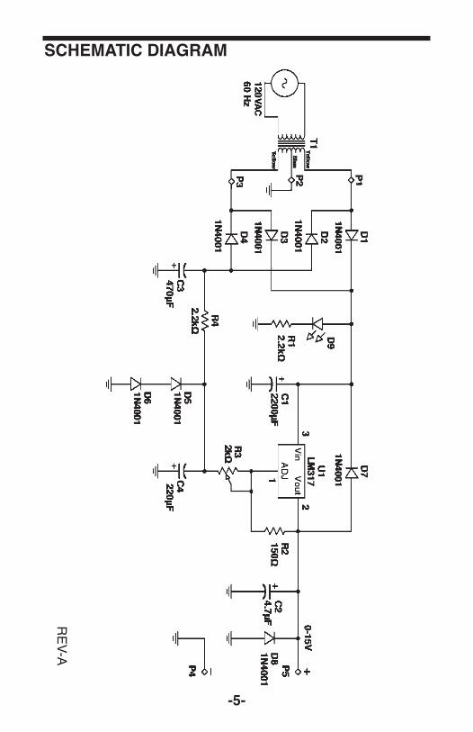
SCHEMATIC DIAGRAM
RE
V-A
-5-

-6-
PARTS LIST
RESISTORSQty. Symbol Description Part #r 1 R2 150W 5% 1/4W 131500r 2 R1, R4 2.2kW 5% 1/4W 142200r 1 R3 2kW Potentiometer 192421
CAPACITORSQty. Symbol Description Part #r 1 C2 4.7mF 50V Electrolytic 264747r 1 C4 220mF 16V Electrolytic 282244r 1 C3 470mF 35V Electrolytic 284746r 1 C1 2,200mF 35V Electrolytic 292226
SEMICONDUCTORSQty. Symbol Description Part #r 8 D1-8 1N4001 Diode 314001r 1 U1 LM317 Regulator 330317r 1 D9 LED Red 350002
MISCELLANEOUSQty. Symbol Part #r 1 Transformer YD-1485 440111r 1 PC board 510002r 1 Heat sink 615009r 1 Knob 622009r 1 Case top 623061r 1 Case bottom 623062r 1 Strain relief 2-wire 624002r 1 Binding post black 625031r 2 Nut binding post 625031HNr 2 Lockwasher binding post 625031LWr 1 Binding post red 625032r 4 Screw 3 x 8mm 641102r 1 Screw 4-40 x 1/4” 641430r 2 Screw 6-32 x 3/8” Blk 641652r 1 Nut 7mm 644101r 1 Nut 4-40 644400r 2 Nut 6-32 644600r 1 Washer flat 8 x 14mm 645101r 4 Washer fiber #6 645602r 2 Lockwasher #6 646600r 4 Rubber foot 662015r 1 Label top 723071r 1 Line cord 2 wire 862100r 2” Shrink tubing 890120

ELENCO®
150 Carpenter Ave.Wheeling, IL 60090
(847) 541-3800Website: www.elenco.com
e-mail: [email protected]
TWO YEAR WARRANTY
All Elenco® models are guaranteed for twofull years on all parts and service. For thefirst 3 months, your power supply is coveredat absolutely no charge. For the remaining21 months, a nominal service charge isrequired to cover shipping and handling.
When returning merchandise for repair,please include proof of purchase, a briefletter of explanation of problem, andsufficient packing material. Beforereturning any merchandise please callour service department at (847) 541-3800to obtain a return authorization number(RMA).


![6 . Wiring Diagram Legacy/Service Manual/1996 LEGACY RH… · 6-3 [D601] WIRING DIAGRAM 6 . Wiring Diagram 6 . Wiring Diagram Battery current 1 . POWER SUPPLY ROUTING Current from](https://static.fdocuments.in/doc/165x107/6058f70ca8a7ee39513c5dc6/6-wiring-legacyservice-manual1996-legacy-rh-6-3-d601-wiring-diagram-6-.jpg)