Power semiconductor device:...
46
Power semiconductor device: Basics Ichiro Omura Kyushu Institute of Technology Japan Since 1909 IEEE EDS Webinar Dec. 2, 2015 Ichiro Omura Kyushu Inst. Tech.
-
Upload
nguyenlien -
Category
Documents
-
view
249 -
download
11
Transcript of Power semiconductor device:...
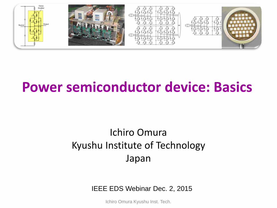
Power semiconductor device: Basics
Ichiro Omura Kyushu Institute of Technology
Japan
Since 1909 IEEE EDS Webinar Dec. 2, 2015
Ichiro Omura Kyushu Inst. Tech.
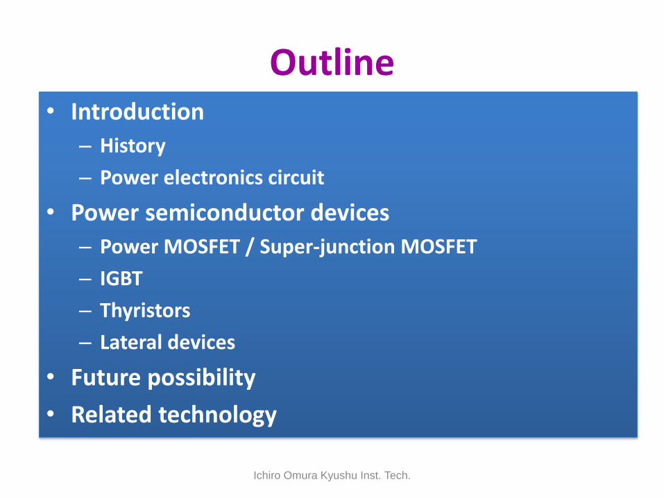
Outline • Introduction
– History
– Power electronics circuit
• Power semiconductor devices
– Power MOSFET / Super-junction MOSFET
– IGBT
– Thyristors
– Lateral devices
• Future possibility
• Related technology
Ichiro Omura Kyushu Inst. Tech.
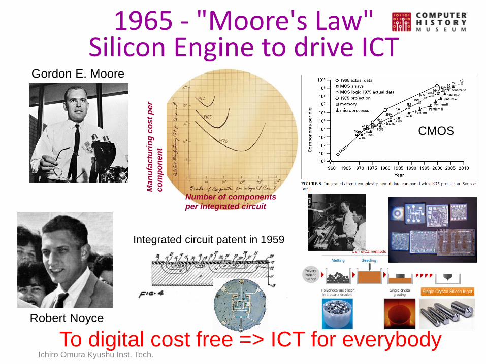
1965 - "Moore's Law" Silicon Engine to drive ICT
Robert Noyce
Integrated circuit patent in 1959
Number of components
per integrated circuit
Ma
nu
fac
turi
ng
co
st
pe
r
co
mp
on
en
t
Gordon E. Moore
CMOS
To digital cost free => ICT for everybody Ichiro Omura Kyushu Inst. Tech.
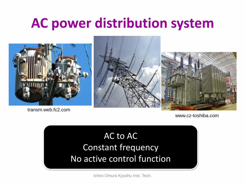
AC power distribution system
Ichiro Omura Kyushu Inst. Tech.
www.cz-toshiba.com
transm.web.fc2.com
AC to AC Constant frequency
No active control function
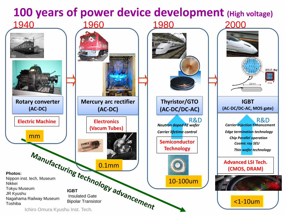
100 years of power device development (High voltage)
Rotary converter (AC-DC)
Semiconductor Technology
Thyristor/GTO (AC-DC/DC-AC)
IGBT (AC-DC/DC-AC, MOS gate)
Electronics (Vacum Tubes)
Neutron doped FZ wafer
Carrier lifetime control
R&D Electric Machine
mm
0.1mm
10-100um
<1-10um
Advanced LSI Tech. (CMOS, DRAM)
1940 1960 1980 2000
Ichiro Omura Kyushu Inst. Tech.
Mercury arc rectifier (AC-DC)
Photos:
Nippon inst. tech, Museum
Nikkei
Tokyu Museum
JR Kyushu
Nagahama Railway Museum
Toshiba
IGBT
Insulated Gate
Bipolar Transistor
Thin wafer technology
Cosmic ray SEU
Chip Parallel operation
Carrier Injection Enhancement
Edge termination technology
R&D
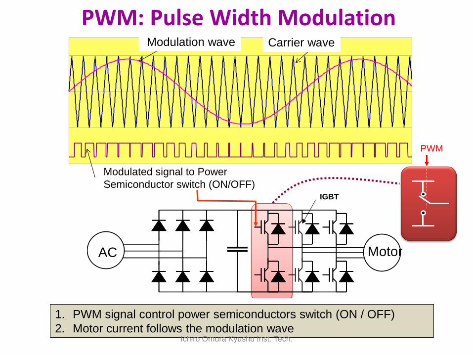
PWM: Pulse Width Modulation
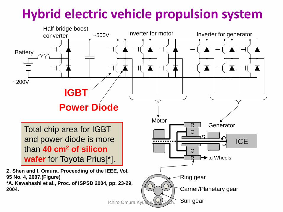
MotorAC
IGBT
PDS: Power Drive System
Carrier wave Modulation wave
Modulated signal to Power
Semiconductor switch (ON/OFF)
1. PWM signal control power semiconductors switch (ON / OFF)
2. Motor current follows the modulation wave
PWM
Ichiro Omura Kyushu Inst. Tech.
C
C
R
R
Ring gear
Sun gear
Carrier/Planetary gear
ICE
Motor Generator
Inverter for motor Inverter for generator
to Wheels
Half-bridge boost
converter
Battery
S
IGBT
Power Diode
Z. Shen and I. Omura. Proceeding of the IEEE, Vol.
95 No. 4, 2007.(Figure)
*A. Kawahashi et al., Proc. of ISPSD 2004, pp. 23-29,
2004.
Total chip area for IGBT
and power diode is more
than 40 cm2 of silicon
wafer for Toyota Prius[*].
Hybrid electric vehicle propulsion system
~200V
~500V
Ichiro Omura Kyushu Inst. Tech.
Power Semiconductor Devices
Ichiro Omura Kyushu Inst. Tech.
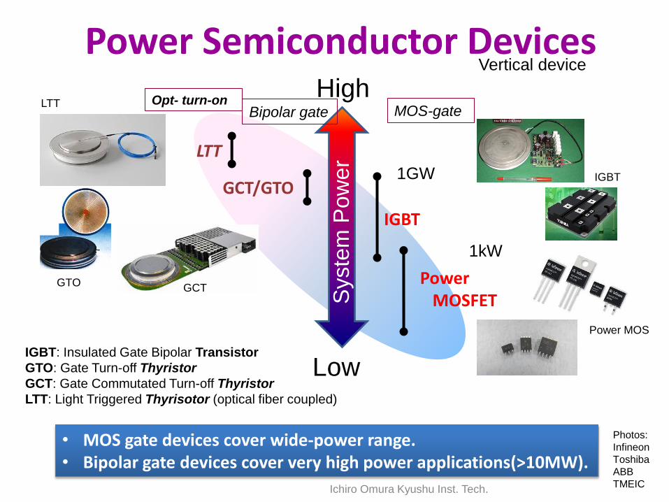
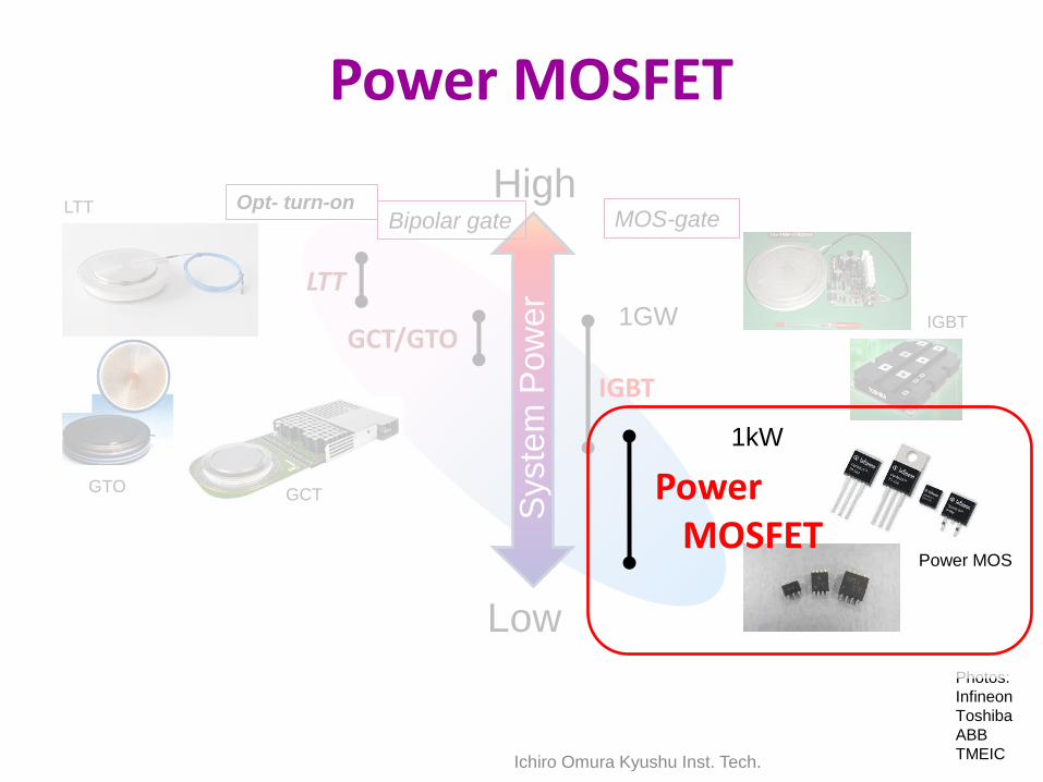
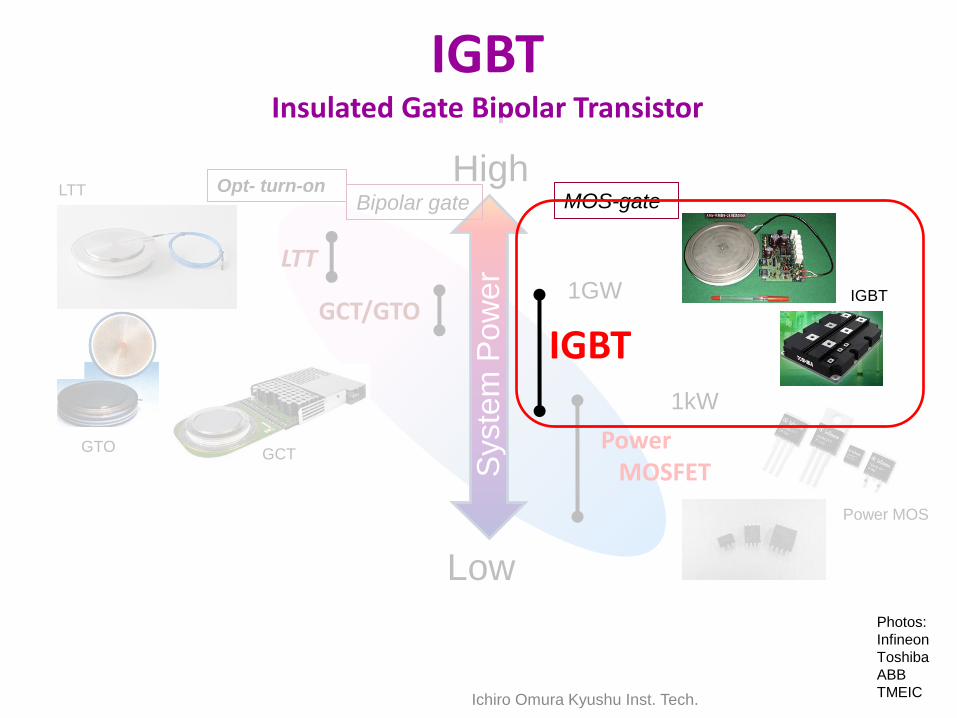
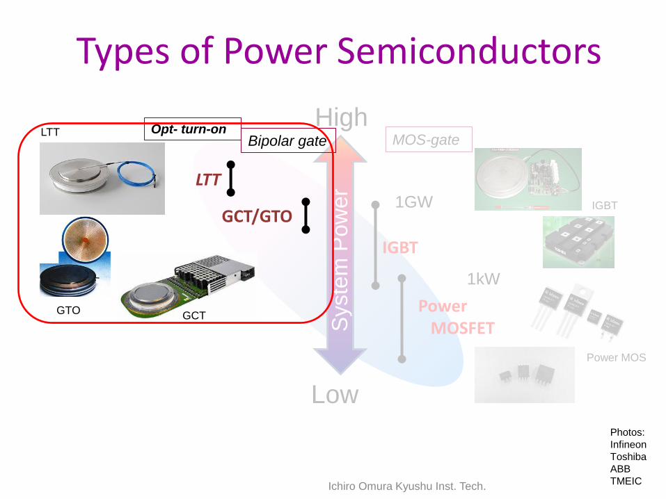
Power Semiconductor Devices
IGBT: Insulated Gate Bipolar Transistor
GTO: Gate Turn-off Thyristor
GCT: Gate Commutated Turn-off Thyristor
LTT: Light Triggered Thyrisotor (optical fiber coupled)
Power MOSFET
Low
High
IGBT
GCT/GTO
Syste
m P
ow
er
MOS-gate Bipolar gate
LTT
• MOS gate devices cover wide-power range. • Bipolar gate devices cover very high power applications(>10MW).
Opt- turn-on
Ichiro Omura Kyushu Inst. Tech.
1kW
1GW
Photos:
Infineon
Toshiba
ABB
TMEIC
GTO GCT
LTT
IGBT
Power MOS
Vertical device
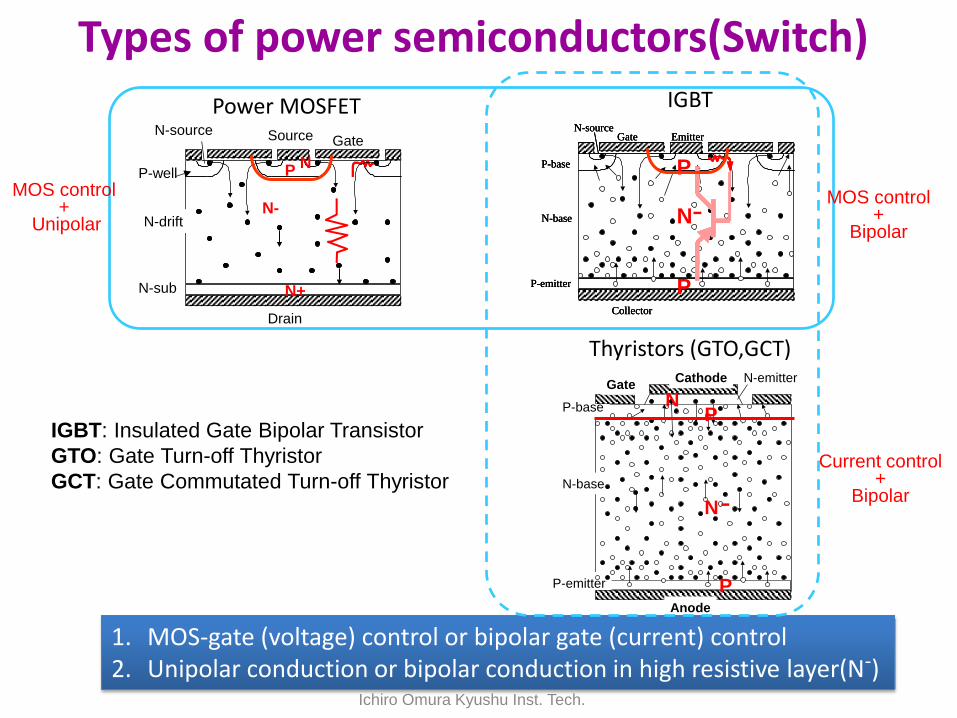
Types of power semiconductors(Switch)
GateN-source Source
Drain
N-sub
P-well
N-drift
P-base
N-base
N-emitter
P-emitter
GateCathode
Anode
N
P
PN
GateN-source
Emitter
Collector
P-emitter
P-base
N-base
P
P
N
GateN-source
Emitter
Collector
P-emitter
P-base
N-base
GateN-source
Emitter
Collector
P-emitter
P-base
N-base
P
P
N
Power MOSFET IGBT
Thyristors (GTO,GCT)
IGBT: Insulated Gate Bipolar Transistor
GTO: Gate Turn-off Thyristor
GCT: Gate Commutated Turn-off Thyristor
1. MOS-gate (voltage) control or bipolar gate (current) control 2. Unipolar conduction or bipolar conduction in high resistive layer(N-)
N+
P
N-
-
N
-
Ichiro Omura Kyushu Inst. Tech.
MOS control +
Unipolar
MOS control +
Bipolar
Current control +
Bipolar
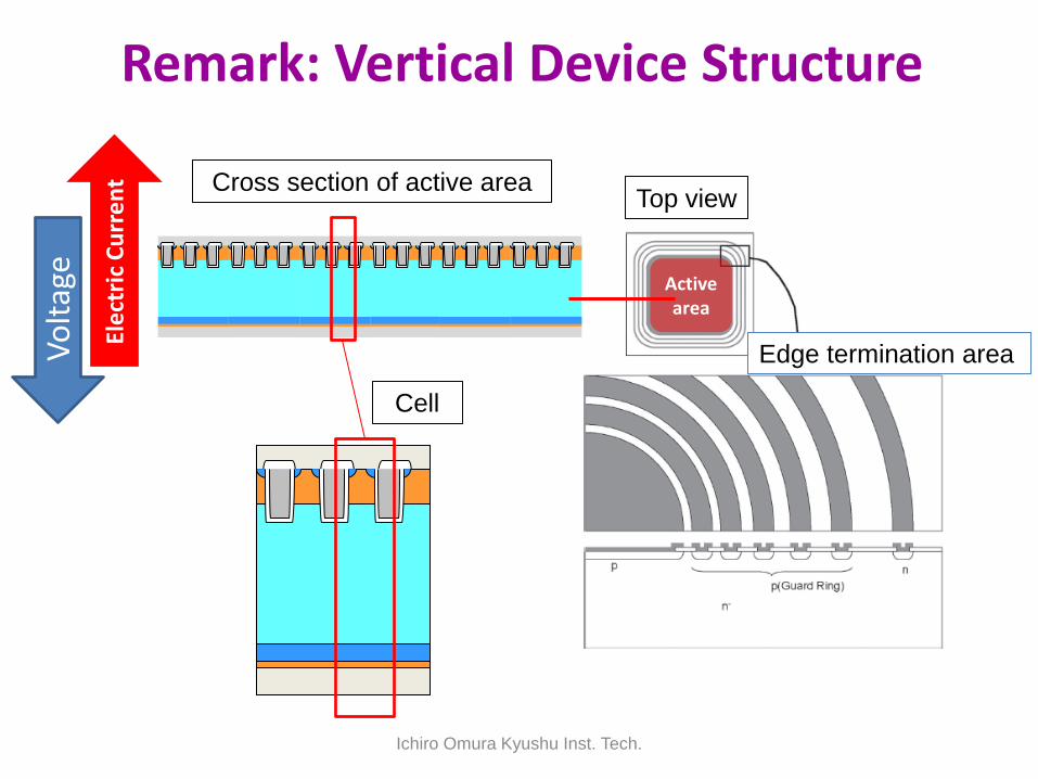
Remark: Vertical Device Structure
Edge termination area
Ele
ctri
c C
urr
en
t
Vo
ltag
e
Ichiro Omura Kyushu Inst. Tech.
Top view Cross section of active area
Cell
Active area
Power MOSFET
Low
High
IGBT
GCT/GTO
Syste
m P
ow
er
MOS-gate Bipolar gate
LTT
Opt- turn-on
Ichiro Omura Kyushu Inst. Tech.
1GW
Photos:
Infineon
Toshiba
ABB
TMEIC
GTO GCT
LTT
IGBT
1kW
Power MOS
Power MOSFET
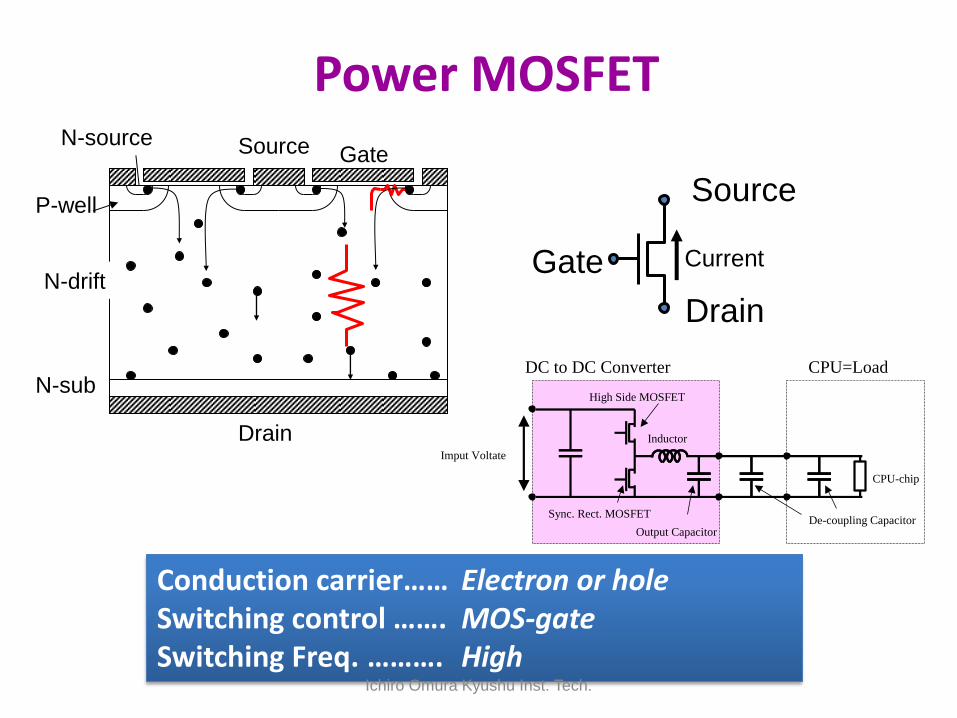
Power MOSFET
Gate N-source Source
Drain
N-sub
P-well
N-drift
Conduction carrier…… Electron or hole Switching control ……. MOS-gate Switching Freq. ………. High
Source
Drain
Gate
De-coupling Capacitor
Imput Voltate
Sync. Rect. MOSFET
High Side MOSFET
Inductor
Output Capacitor
CPU-chip
DC to DC Converter CPU=Load
Current
Ichiro Omura Kyushu Inst. Tech.
Function of N-drift layer
Source
Drain
(VB)
Ey
drift
dy
DL
E
dy
dEqN
dE
S
D
G
Source
Drain
Ey
Charge
neutrality
Voltage Blocking Conduction
p
n+
n-drift
drift
condDncondDnn
L
VNqENqJ
condE
electron
driftL
Function of N-drift layer: 1. Voltage blocking (higher breakdown voltage) 2. Current conduction (lower resistivity)
Blocking state (Poisson eq.) Conduction state (current eq.)
n: electron mobility
donor
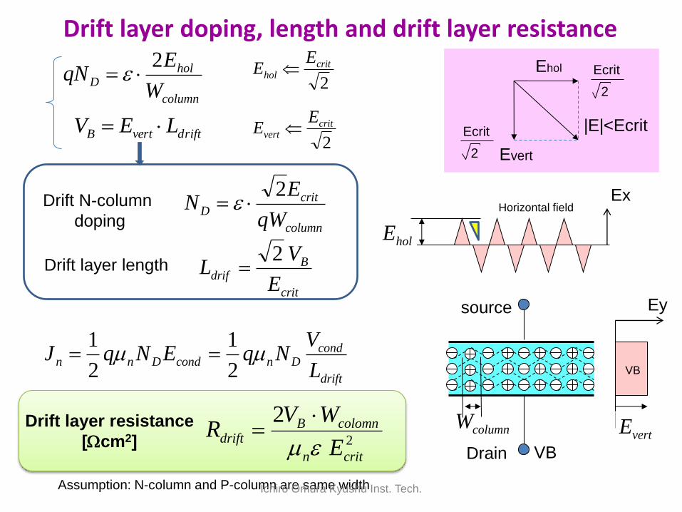
Ichiro Omura Kyushu Inst. Tech.
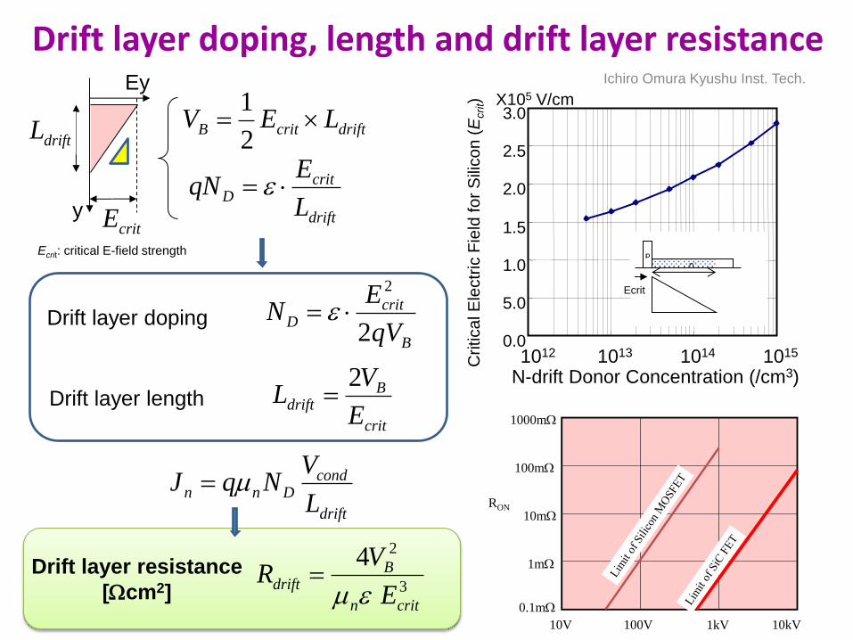
driftcritB LEV 2
1
3
24
critn
Bdrift
E
VR
Ey
critE
driftL
y drift
critD
L
EqN
Drift layer doping, length and drift layer resistance
0.0
5.0
1.0
1.5
2.0
2.5
3.0
1012 1013 1014 1015
X105 V/cm
Critica
l E
lectr
ic F
ield
fo
r S
ilico
n (
Ecrit)
N-drift Donor Concentration (/cm3)
p n-
Ecrit
B
critD
qV
EN
2
2
crit
Bdrift
E
VL
2
Drift layer doping
Drift layer length
drift
condDnn
L
VNqJ
Drift layer resistance
[Wcm2]
10V 100V 1kV 10kV
0.1mW
1mW
10mW
100mW
1000mW
RON
Ecrit: critical E-field strength
Ichiro Omura Kyushu Inst. Tech.
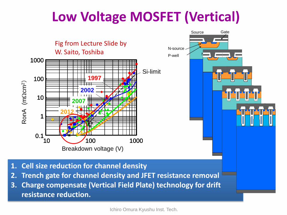
1. Cell size reduction for channel density 2. Trench gate for channel density and JFET resistance removal 3. Charge compensate (Vertical Field Plate) technology for drift
resistance reduction.
Low Voltage MOSFET (Vertical)
N-drift layerP-well
N-source
GateSource
Drain
Breakdown voltage (V)
10 100 1000
1000
100
10
1
0.1
RonA
(mW
cm
2)
Si-limit
10 100 1000
1000
100
10
1
0.110 100 1000
1000
100
10
1
0.1
1997
2002
2007
2012
Fig from Lecture Slide by W. Saito, Toshiba
Ichiro Omura Kyushu Inst. Tech.
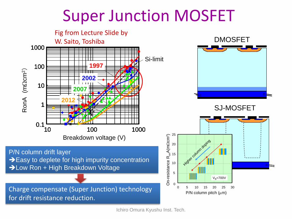
DMOSFET
P/N column drift layer
Easy to deplete for high impurity concentration
Low Ron + High Breakdown Voltage
SJ-MOSFET
0
5
10
15
20
25
0 5 10 15 20 25 30
P/N column pitch (m)
On-r
esis
tan
ce
Ro
nA
(mW
cm
2)
VB=700V
Hig
her c
olum
n do
ping
Breakdown voltage (V)
10 100 1000
1000
100
10
1
0.1
RonA
(mW
cm
2)
Si-limit
10 100 1000
1000
100
10
1
0.110 100 1000
1000
100
10
1
0.1
1997
2002
2007
2012
Fig from Lecture Slide by W. Saito, Toshiba
Super Junction MOSFET
Charge compensate (Super Junction) technology for drift resistance reduction.
Ichiro Omura Kyushu Inst. Tech.
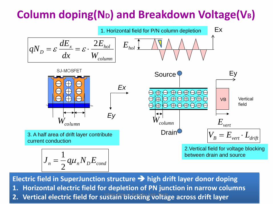
Column doping(ND) and Breakdown Voltage(VB)
Source
Drain
Ey
holE
Ex
VB
Ex
Ey
1. Horizontal field for P/N column depletion
Vertical
field
column
holxD
W
E
dx
dEqN
2
columnWcolumnW
vertE
driftvertB LEV
2.Vertical field for voltage blocking
between drain and source
Electric field in SuperJunction structure high drift layer donor doping 1. Horizontal electric field for depletion of PN junction in narrow columns 2. Vertical electric field for sustain blocking voltage across drift layer
condDnn ENqJ 2
1
3. A half area of drift layer contribute
current conduction
Ichiro Omura Kyushu Inst. Tech.
VB
Ehol
Evert
|E|<Ecrit
2
Ecrit
2
Ecrit
column
critD
qW
EN
2
source
Drain
Ey
holE
Ex
VB
Horizontal field
columnWvertE
drift
condDncondDnn
L
VNqENqJ
2
1
2
1
Drift N-column
doping
Drift layer length
driftvertB LEV
column
holD
W
EqN
2
2
crithol
EE
2
critvert
EE
crit
Bdrif
E
VL
2
Drift layer resistance
[Wcm2] 2
2
critn
colomnBdrift
E
WVR
Drift layer doping, length and drift layer resistance
Assumption: N-column and P-column are same width Ichiro Omura Kyushu Inst. Tech.
1GW
IGBT Insulated Gate Bipolar Transistor
Low
High
GCT/GTO
Syste
m P
ow
er
Bipolar gate
LTT
Opt- turn-on
Ichiro Omura Kyushu Inst. Tech.
Photos:
Infineon
Toshiba
ABB
TMEIC
GTO GCT
LTT
Power MOSFET
1kW
Power MOS
IGBT
MOS-gate
IGBT
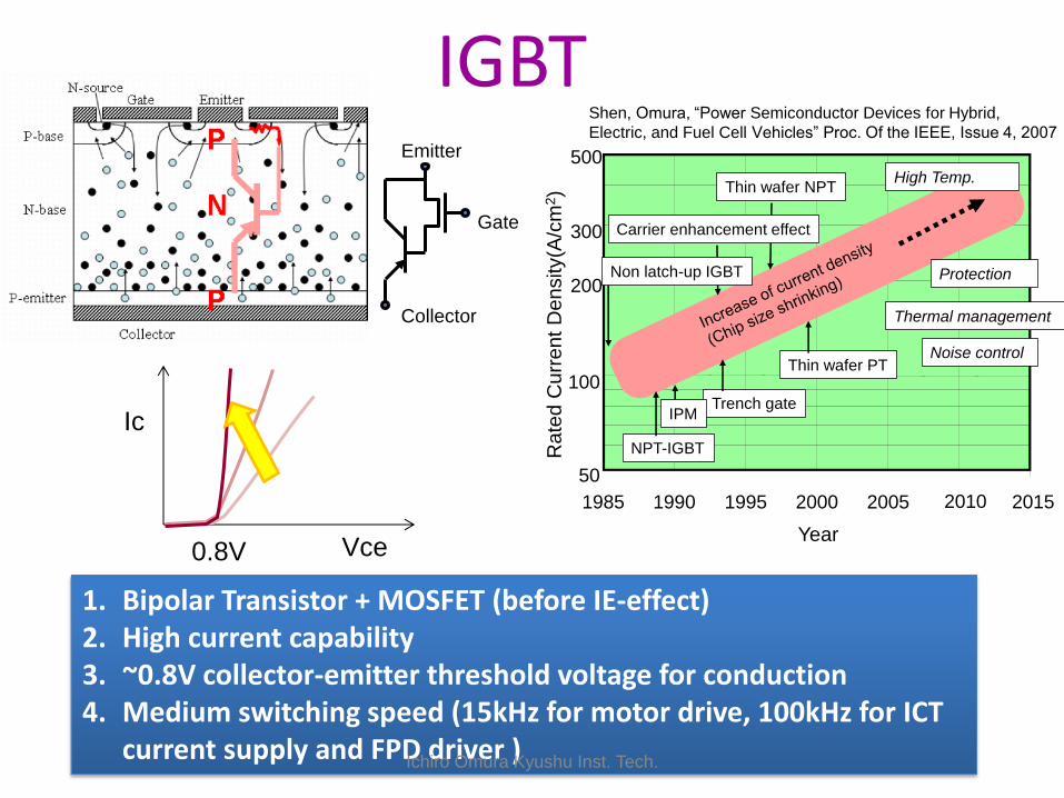
1. Bipolar Transistor + MOSFET (before IE-effect) 2. High current capability 3. ~0.8V collector-emitter threshold voltage for conduction 4. Medium switching speed (15kHz for motor drive, 100kHz for ICT
current supply and FPD driver )
Collector
Gate
Emitter
IGBT
50
100
1985 1990 1995 2000 2005
200
300
500
Rate
d C
urr
ent
Density(A
/cm
2) Thin wafer NPT
Thin wafer PT
Trench gate
NPT-IGBT
Carrier enhancement effect
Non latch-up IGBT
IPM
Year
2010 2015
Thermal management
High Temp.
Protection
Noise control
Vce
Ic
0.8V
Shen, Omura, “Power Semiconductor Devices for Hybrid,
Electric, and Fuel Cell Vehicles” Proc. Of the IEEE, Issue 4, 2007
Ichiro Omura Kyushu Inst. Tech.
Operation mechanism of IGBT
Ionized impurity (donor)
0E
0E
0E
0E
Electron
0)(
nNqdx
EdD
0)(
npNqdx
EdD
npND , npni
Conduction modulation in N-base
positive negative
Hole
)(2 np
kT
q
i enpn
2
inpn
GateN-source
Emitter
Collector
P-emitter
P-base
N-base
P
P
N
GateN-source
Emitter
Collector
P-emitter
P-base
N-base
P
P
N
np
Vce
Ic
0.8V
IGBT
MOSFET
PN-junction built-in
potential
Conduction
modulation
Unipolar
N-base
Conduction modulation 1. Both hole and electron contribute to current
conduction 2. High stored carrier density in N-base (>1016cm-3) 3. Built-in voltage with the stored carrier
Ichiro Omura Kyushu Inst. Tech.
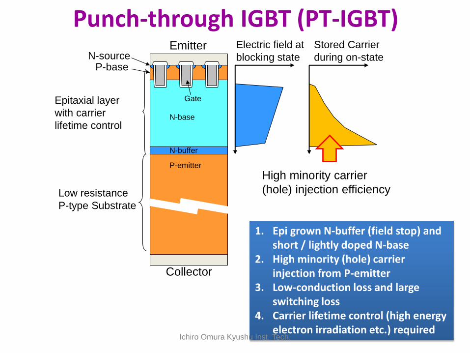
Epitaxial layer
with carrier
lifetime control
Electric field at
blocking state
Low resistance
P-type Substrate
Stored Carrier
during on-state
P-emitter
N-buffer
N-base
P-base N-source
Gate
Emitter
Collector
High minority carrier
(hole) injection efficiency
Punch-through IGBT (PT-IGBT)
1. Epi grown N-buffer (field stop) and short / lightly doped N-base
2. High minority (hole) carrier injection from P-emitter
3. Low-conduction loss and large switching loss
4. Carrier lifetime control (high energy electron irradiation etc.) required
Ichiro Omura Kyushu Inst. Tech.
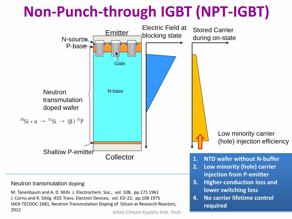
Electric Field at
blocking state
Neutron
transmutation
doped wafer
Stored Carrier
during on-state
Shallow P-emitter
N-base
P-base N-source
Gate
Emitter
Collector
M. Tanenbaum and A. D. Mills J. Electrochem. Soc., vol. 108, pp.171 1961 J. Cornu and R. Sittig IEEE Trans. Electron Devices, vol. ED-22, pp.108 1975 IAEA-TECDOC-1681, Neutron Transmutation Doping of Silicon at Research Reactors, 2012
Neutron transmutation doping
Low minority carrier
(hole) injection efficiency
Non-Punch-through IGBT (NPT-IGBT)
1. NTD wafer without N-buffer 2. Low minority (hole) carrier
injection from P-emitter 3. Higher-conduction loss and
lower switching loss 4. No carrier lifetime control
required Ichiro Omura Kyushu Inst. Tech.
Electric field at
blocking state
Stored Carrier
during on-state
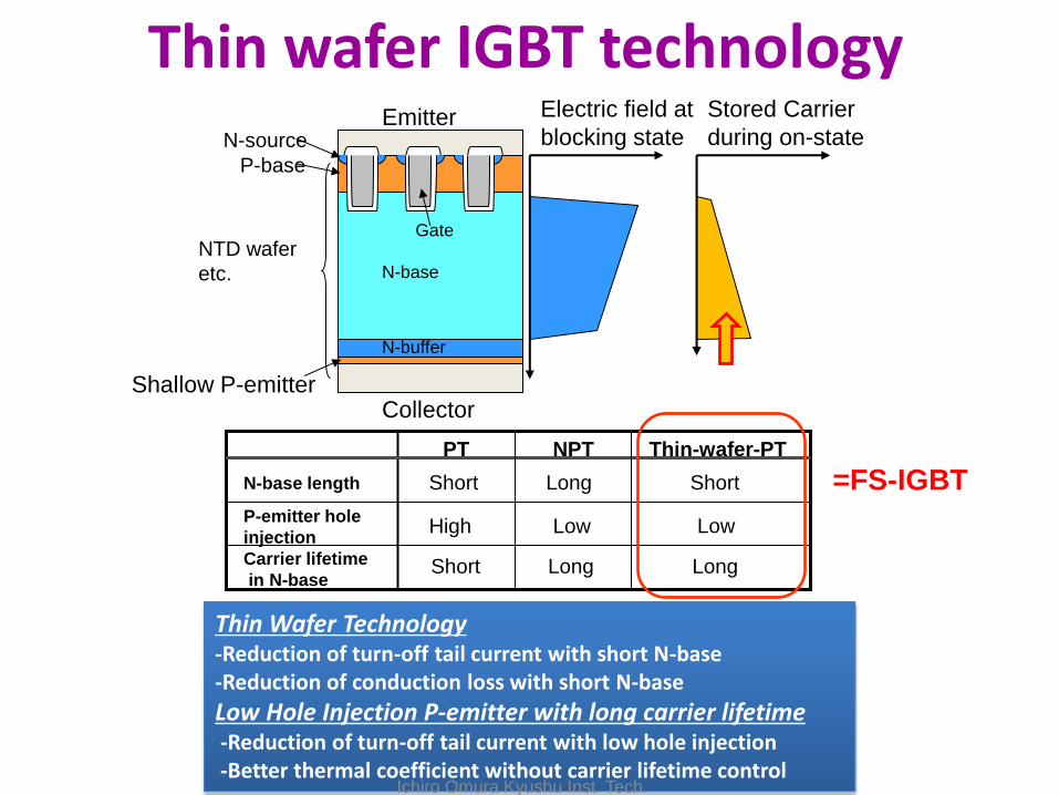
N-buffer
N-base
Shallow P-emitter
NTD wafer
etc.
P-base
N-source
Gate
Emitter
Collector
Thin wafer IGBT technology
N-base length Short Long Short
Carrier lifetime
in N-base Short Long Long
P-emitter hole
injection High Low Low
PT NPT Thin-wafer-PT
Thin Wafer Technology -Reduction of turn-off tail current with short N-base -Reduction of conduction loss with short N-base
Low Hole Injection P-emitter with long carrier lifetime -Reduction of turn-off tail current with low hole injection -Better thermal coefficient without carrier lifetime control
Ichiro Omura Kyushu Inst. Tech.
=FS-IGBT
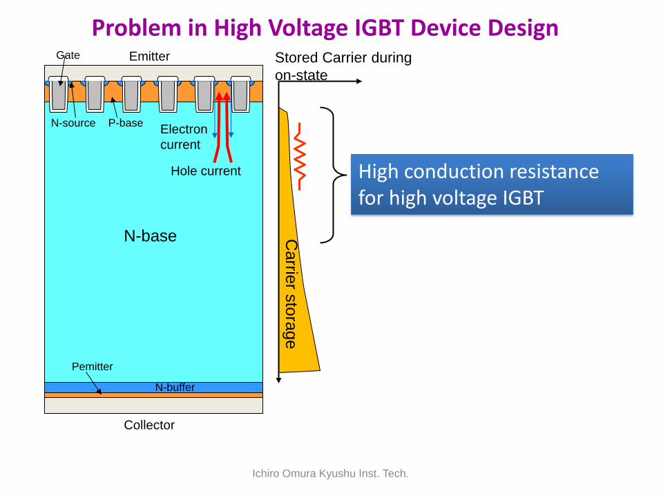
Stored Carrier during
on-state
N-base
Pemitter
N-buffer
P-base N-source
Gate
Collector
Emitter
Hole current
Electron
current
Problem in High Voltage IGBT Device Design
High conduction resistance for high voltage IGBT
Carrie
r sto
rage
Ichiro Omura Kyushu Inst. Tech.
Stored Carrier
during on-state
Pemitter
N-buffer
P-base
N-source
Gate
Collector
Emitter
Hole current
Electron
current
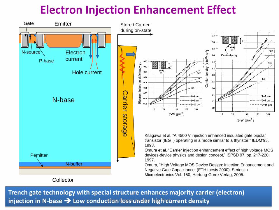
Electron Injection Enhancement Effect
Trench gate technology with special structure enhances majority carrier (electron) injection in N-base Low conduction loss under high current density
Kitagawa et al. “A 4500 V injection enhanced insulated gate bipolar
transistor (IEGT) operating in a mode similar to a thyristor,” IEDM’93,
1993.
Omura et al. “Carrier injection enhancement effect of high voltage MOS
devices-device physics and design concept,” ISPSD 97, pp. 217-220,
1997.
Omura, “High Voltage MOS Device Design: Injection Enhancement and
Negative Gate Capacitance, (ETH thesis 2000), Series in
Microelectronics Vol. 150, Hartung-Gorre Verlag, 2005.
N-base
Carrie
r sto
rage
Ichiro Omura Kyushu Inst. Tech.
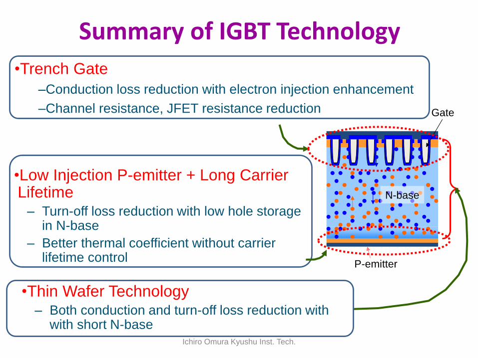
Summary of IGBT Technology
N-base
P-emitter
Gate
•Thin Wafer Technology – Both conduction and turn-off loss reduction with
with short N-base
•Trench Gate
–Conduction loss reduction with electron injection enhancement
–Channel resistance, JFET resistance reduction
•Low Injection P-emitter + Long Carrier Lifetime
– Turn-off loss reduction with low hole storage in N-base
– Better thermal coefficient without carrier lifetime control
Ichiro Omura Kyushu Inst. Tech.
N-base
Pemitter
N-buffer
Floating P
Gate
Collector
Emitter
Hole
current
Electron
current
Ey
Voltage blocking
E-field
n
Conduction (flat carrier distribution is assumed)
Ey
E-field
Ch
arge neu
trality
p
Electron hole
storedn
crit
Bbasen
crit
B
E
VL
E
V 2
storednnp
N-base length
Stored Carrier
density
Conduction and Breakdown Voltage
i
stroedinbuilt
n
n
q
kTV ln2
critstoredpn
BbaseN
Enq
VR
)(
2~1
N-base conduction
resistance
PN-junction built-in
potential
Vce 0.8V
IGBT
MOSFET Ic
Ichiro Omura Kyushu Inst. Tech.
DMOSFET
Drift Layer Doping
(Stored carrier density)
Drift Layer Length
(N-base length) crit
Bdrif
E
VL
2
Drift Layer Resistance
(N-base conduction
resistance) 3
24
critn
Bdrift
E
VR
B
critD
qV
EN
2
2
column
critD
qW
EN
2
crit
Bdrif
E
VL
2
2
2
critn
colomnBdrift
E
WVR
Device Structure
Assumption: N-column and P-
column are same width
IGBT
N-base
Pemitter
N-buffer
Floating P
Gate
Collector
Emitter
Hole
current
Electron
current
storedn
crit
Bbasen
E
VL
2~1
critstoredpn
BbaseN
Enq
VR
)(
2~1
(flat carrier stored carrier
distribution is assumed
(>1016cm-3)
SJ-MOSFET
PN-junction
built-in potential none none
i
storedinbuilt
n
n
q
kTV ln2
600V class device 80-100 mWcm2 <10 mWcm2 ~1.5V at 200A/cm2
Omura et. al, International Workshop on Physics of Semiconductor Devices, 2007. IWPSD 2007, pp. 781 – 786, 2007
.
Ichiro Omura Kyushu Inst. Tech.
DMOSFET
Device Structure
IGBT
N-base
Pemitter
N-buffer
Floating P
Gate
Collector
Emitter
Hole
current
Electron
current
SJ-MOSFET
V-I
characteristics
Omura et. al, International Workshop on Physics of Semiconductor Devices, 2007. IWPSD 2007, pp. 781 – 786, 2007
.
Switching
charge (turn-off
charge)
Vce
Ic
inbuiltV
VDS
ID baseNR
VDS
ID driftON RR
driftON RR
Charge in main-junction
capacitance Stored carrier sweep out
PN-column depletion
charge
Ichiro Omura Kyushu Inst. Tech.
Types of Power Semiconductors
Low
High
Syste
m P
ow
er
Ichiro Omura Kyushu Inst. Tech.
Photos:
Infineon
Toshiba
ABB
TMEIC
Power MOSFET
1kW
Power MOS
IGBT
MOS-gate
1GW IGBT GCT/GTO
Bipolar gate
LTT
Opt- turn-on
GTO GCT
LTT
N-emitter
N-base
Cathode Anode
Stored carrier concentration
under current conduction
Impurity
concentr
ation
P-base P-emitter
Light Triggered Thyristor(LTT) Photos: http://dbnst.nii.ac.jp/
Ichiro Omura Kyushu Inst. Tech.
Forward
blocking Conduction
Reverse
blocking
Trigger pulse
1. PNPN structure 2. Light triggered turn-on 3. Cannot turn-off by gate 4. One wafer per one device 5. Pressure contact package 6. Highest power per single semiconductor
1.4GW system by Toshiba
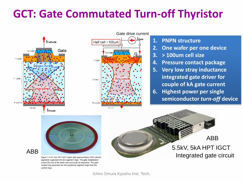
ABB GTO(GCT)
Integrated gate circuit
5.5kV, 5kA HPT IGCT
Gate drive current
ABB
ABB
GCT: Gate Commutated Turn-off Thyristor
1. PNPN structure 2. One wafer per one device 3. > 100um cell size 4. Pressure contact package 5. Very low stray inductance
integrated gate driver for couple of kA gate current
6. Highest power per single semiconductor turn-off device
Ichiro Omura Kyushu Inst. Tech.
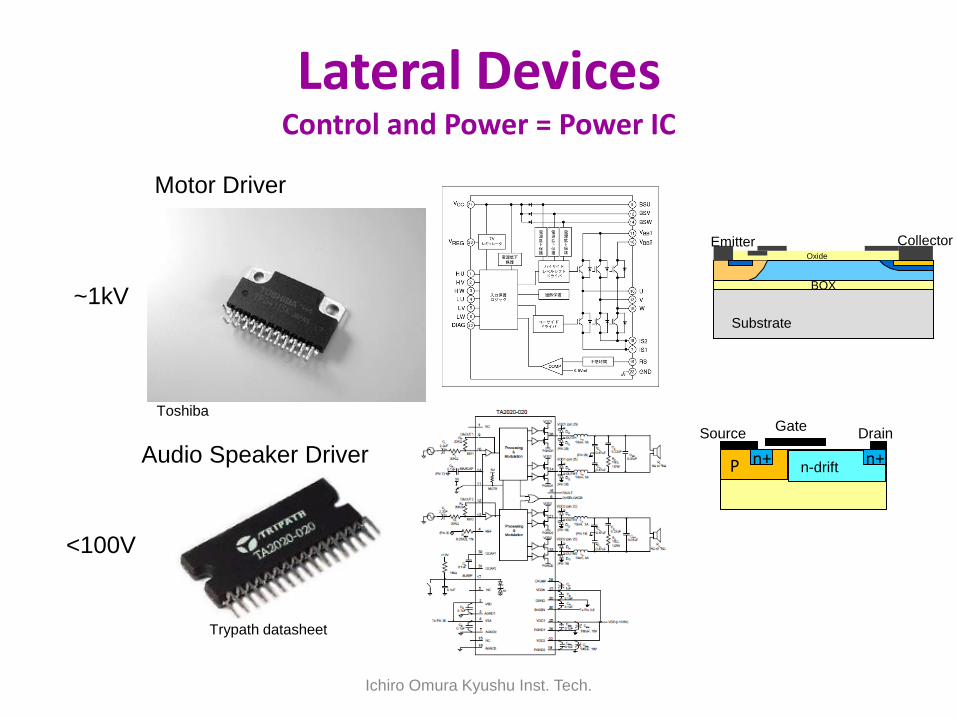
Motor Driver
Audio Speaker Driver
~1kV
<100V
Oxide
BOX
Emitter Collector
Substrate
Lateral Devices Control and Power = Power IC
P n+ n+ n-drift
Source Drain Gate
Trypath datasheet
Toshiba
Ichiro Omura Kyushu Inst. Tech.
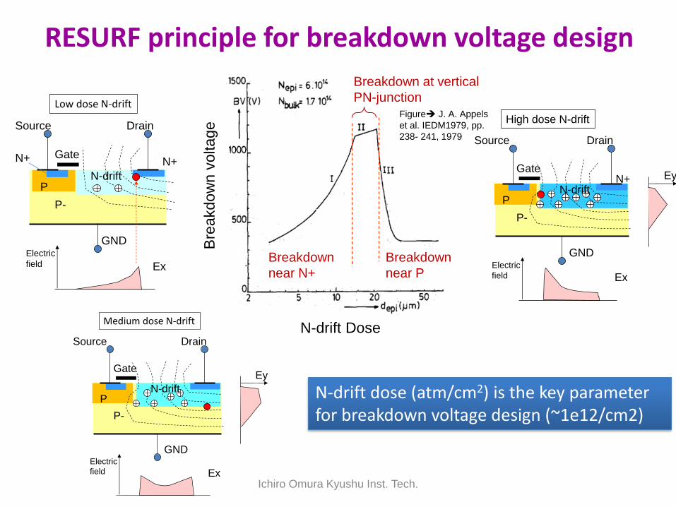
Breakdown at vertical
PN-junction
N-drift Dose
Bre
akdo
wn v
oltag
e
Breakdown
near N+
Breakdown
near P
RESURF principle for breakdown voltage design
N-drift dose (atm/cm2) is the key parameter for breakdown voltage design (~1e12/cm2)
Figure J. A. Appels
et al. IEDM1979, pp.
238- 241, 1979
P
P-
N+
Gate
Source Drain
High dose N-drift
GND
Ey
ExElectric
field
N-driftN+
P
P-
N+
Gate
Source Drain
Ex
Low dose N-drift
GNDElectric
field
N+ N+
N-drift
P
P-
N+
Gate
Source Drain
Medium dose N-drift
GND
Ey
ExElectric
field
N-drift
Ichiro Omura Kyushu Inst. Tech.
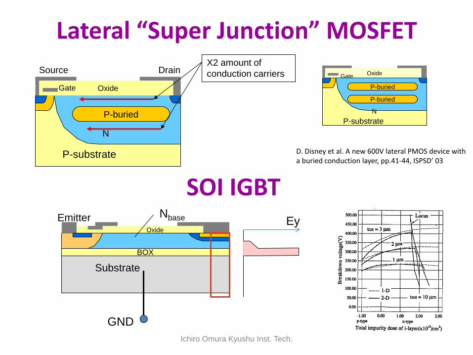
Oxide
D. Disney et al. A new 600V lateral PMOS device with a buried conduction layer, pp.41-44, ISPSD’ 03
Gate
P-buried
N
P-substrate
Drain Source X2 amount of
conduction carriers Oxide Gate
P-buried
N
P-substrate
P-buried
Lateral “Super Junction” MOSFET
Ichiro Omura Kyushu Inst. Tech.
SOI IGBT
Oxide
BOX
GND
Emitter
Substrate
Nbase Ey
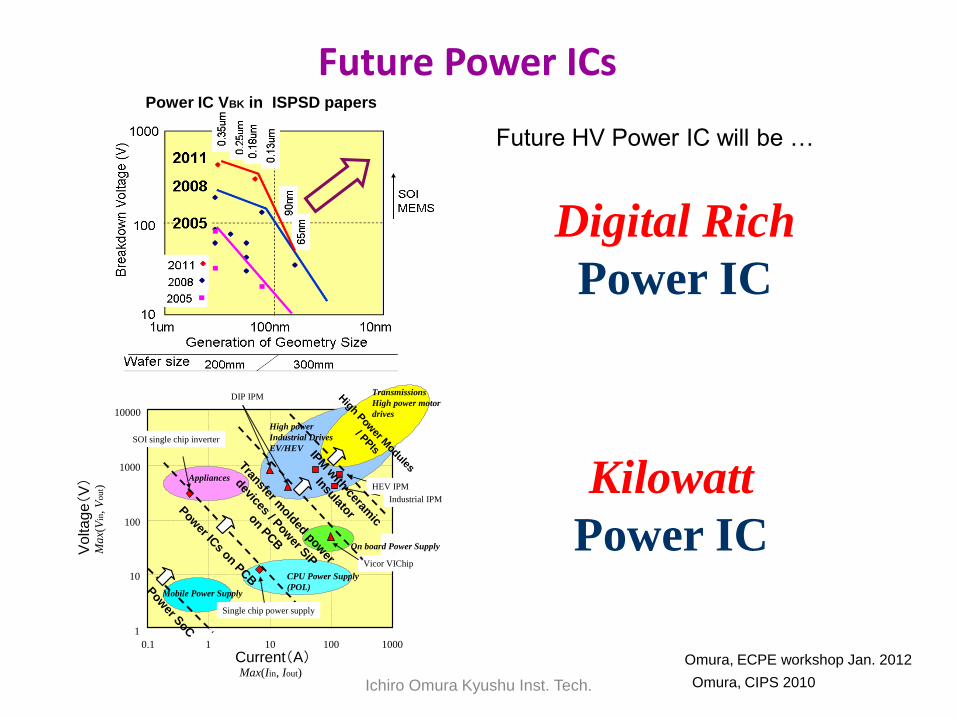
Future Power ICs Power IC VBK in ISPSD papers
Digital Rich
Power IC
Omura, ECPE workshop Jan. 2012
Future HV Power IC will be …
Ichiro Omura Kyushu Inst. Tech.
1
10
100
1000
10000
0.1 1 10 100 1000
Current(A)
Vo
lta
ge(V)
Max(
Vin
, V
ou
t)
CPU Power Supply
(POL)
Appliances
Mobile Power Supply
Transmissions
High power motor
drives
Vicor VIChip
DIP IPM
Max(Iin, Iout)
HEV IPM
Pow
er ICs on P
CB
SOI single chip inverter
Single chip power supply
Transfer molded pow
er
devices / Pow
er SiP
on PCB
IPM
with ceram
ic
Insulator
Pow
er SoC
High power
Industrial Drives
EV/HEV
High P
ower M
odules
/ PPIs
On board Power Supply
Industrial IPM
Omura, CIPS 2010
Kilowatt
Power IC

Future Possibility
Ichiro Omura Kyushu Inst. Tech.
Ichiro Omura Kyushu Inst. Tech.
Power Integrated
Circuit area
Power Integrated
Circuit area
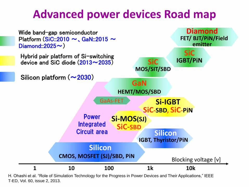
GaN HEMT/MOS/SBD
Wide band-gap semiconductor Platform (SiC::2010 ~、GaN::2015 ~ Diamond::2025~)
SiC MOS/SIT/SBD
SiC IGBT/PiN
Blocking voltage [v]
1 10 100 1k 10k
Diamond FET/ BJT/PiN/Field
emitter
CMOS, MOSFET (SJ)/SBD, PiN
IGBT, Thyristor/PiN
Si-MOS(SJ) SiC-SBD
Si-IGBT SiC-SBD, SiC-PiN
Silicon
Silicon
GaAs-FET
Advanced power devices Road map
Silicon platform (~2030)
Hybrid pair platform of Si-switching device and SiC diode (2013~2035)
H. Ohashi et al. “Role of Simulation Technology for the Progress in Power Devices and Their Applications,” IEEE
T-ED, Vol. 60, issue 2, 2013.
Future possibility
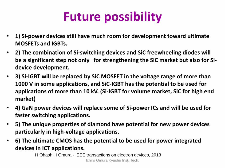
• 1) Si-power devices still have much room for development toward ultimate MOSFETs and IGBTs.
• 2) The combination of Si-switching devices and SiC freewheeling diodes will be a significant step not only for strengthening the SiC market but also for Si-device development.
• 3) Si-IGBT will be replaced by SiC MOSFET in the voltage range of more than 1000 V in some applications, and SiC-IGBT has the potential to be used for applications of more than 10 kV. (Si-IGBT for volume market, SiC for high end market)
• 4) GaN power devices will replace some of Si-power ICs and will be used for faster switching applications.
• 5) The unique properties of diamond have potential for new power devices particularly in high-voltage applications.
• 6) The ultimate CMOS has the potential to be used for power integrated devices in ICT applications.
H Ohashi, I Omura - IEEE transactions on electron devices, 2013
Ichiro Omura Kyushu Inst. Tech.
Related Technology
Ichiro Omura Kyushu Inst. Tech.
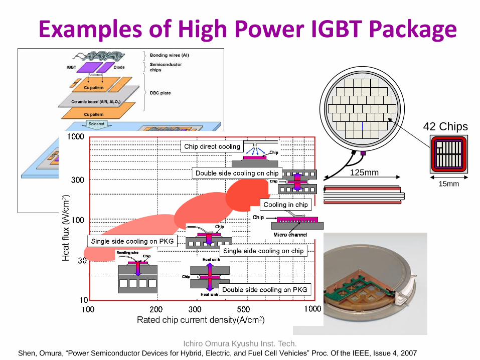
Examples of High Power IGBT Package
125mm
42 Chips
15mm
Shen, Omura, “Power Semiconductor Devices for Hybrid, Electric, and Fuel Cell Vehicles” Proc. Of the IEEE, Issue 4, 2007
Ichiro Omura Kyushu Inst. Tech.
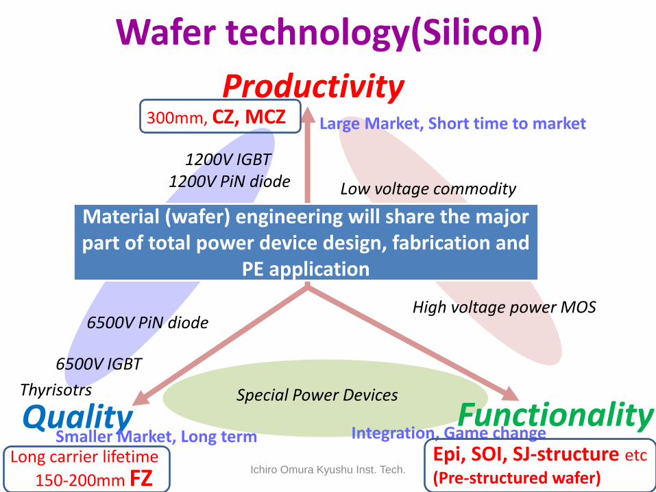
Wafer technology(Silicon)
Productivity
Quality Functionality
Low voltage commodity
Low voltage high spec
6500V IGBT
1200V IGBT 1200V PiN diode
High voltage power MOS
Thyrisotrs
300mm, CZ, MCZ
150-200mm FZ Epi, SOI, SJ-structure etc
(Pre-structured wafer)
Special Power Devices
6500V PiN diode
Long carrier lifetime
Material (wafer) engineering will share the major part of total power device design, fabrication and
PE application
Large Market, Short time to market
Smaller Market, Long term Integration, Game change
Ichiro Omura Kyushu Inst. Tech.
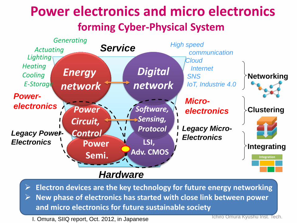
Power electronics and micro electronics forming Cyber-Physical System
Hardware
Micro-
electronics
Service
LSI, Adv. CMOS
Power Semi.
Power Circuit, Control Legacy Power-
Electronics
Energy network
Software, Sensing, Protocol Legacy Micro-
Electronics
Power-
electronics
Digital network
Networking
Clustering
Integrating
Actuating Lighting Heating Cooling E-Storage
High speed
communication
Cloud
Internet
SNS
IoT, Industrie 4.0
I. Omura, SIIQ report, Oct. 2012, in Japanese
Integration
Ichiro Omura Kyushu Inst. Tech.
Generating
Electron devices are the key technology for future energy networking New phase of electronics has started with close link between power
and micro electronics for future sustainable society
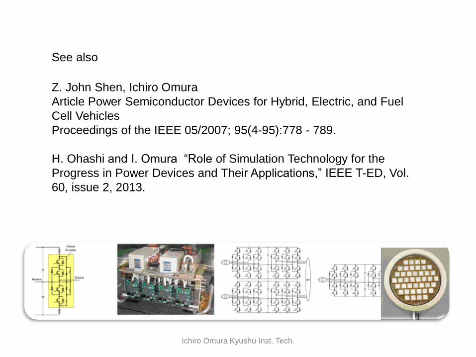
Z. John Shen, Ichiro Omura
Article Power Semiconductor Devices for Hybrid, Electric, and Fuel
Cell Vehicles
Proceedings of the IEEE 05/2007; 95(4-95):778 - 789.
H. Ohashi and I. Omura “Role of Simulation Technology for the
Progress in Power Devices and Their Applications,” IEEE T-ED, Vol.
60, issue 2, 2013.
Ichiro Omura Kyushu Inst. Tech.
See also