Power Reduction Techniques in the Memory Systemmji/asic/tutorial-memory.pdf · Low Power Design for...
20
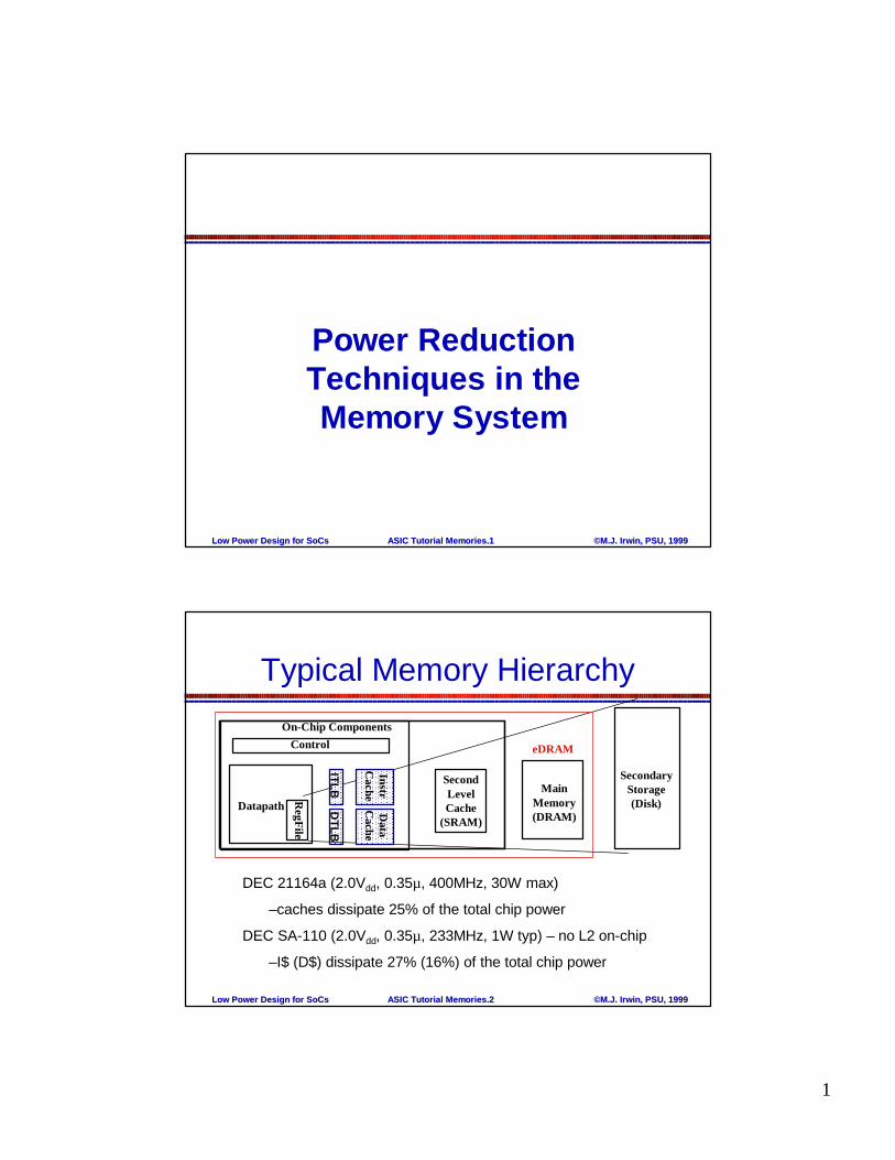
1 ASIC Tutorial Memories. ASIC Tutorial Memories.1 Low Power Design for Low Power Design for SoCs SoCs ©M.J. Irwin, PSU, 1999 M.J. Irwin, PSU, 1999 Power Reduction Techniques in the Memory System ASIC Tutorial Memories. ASIC Tutorial Memories.2 Low Power Design for Low Power Design for SoCs SoCs ©M.J. Irwin, PSU, 1999 M.J. Irwin, PSU, 1999 Typical Memory Hierarchy Control Datapath Secondary Storage (Disk) On-Chip Components RegFile Main Memory (DRAM) Second Level Cache (SRAM) Data Cache Instr Cache ITLB DTLB DEC 21164a (2.0V dd , 0.35μ, 400MHz, 30W max) –caches dissipate 25% of the total chip power DEC SA-110 (2.0V dd , 0.35μ, 233MHz, 1W typ) – no L2 on-chip –I$ (D$) dissipate 27% (16%) of the total chip power eDRAM
Transcript of Power Reduction Techniques in the Memory Systemmji/asic/tutorial-memory.pdf · Low Power Design for...
1
ASIC Tutorial Memories.ASIC Tutorial Memories.11Low Power Design for Low Power Design for SoCsSoCs ©©M.J. Irwin, PSU, 1999M.J. Irwin, PSU, 1999
Power Reduction Techniques in the Memory System
ASIC Tutorial Memories.ASIC Tutorial Memories.22Low Power Design for Low Power Design for SoCsSoCs ©©M.J. Irwin, PSU, 1999M.J. Irwin, PSU, 1999
Typical Memory Hierarchy
Control
Datapath
SecondaryStorage(Disk)
On-Chip Components
RegFile
MainMemory(DRAM)
SecondLevelCache
(SRAM)
Data
Cache
InstrC
ache
ITLBD
TLB
DEC 21164a (2.0Vdd, 0.35µ, 400MHz, 30W max)
–caches dissipate 25% of the total chip power
DEC SA-110 (2.0Vdd, 0.35µ, 233MHz, 1W typ) – no L2 on-chip
–I$ (D$) dissipate 27% (16%) of the total chip power
eDRAM
2
ASIC Tutorial Memories.ASIC Tutorial Memories.33Low Power Design for Low Power Design for SoCsSoCs ©©M.J. Irwin, PSU, 1999M.J. Irwin, PSU, 1999
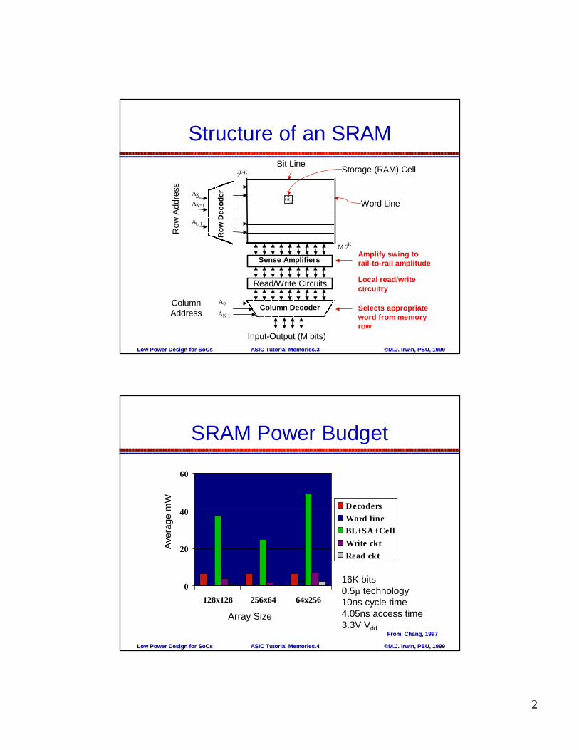
Structure of an SRAM
Amplify swing torail-to-rail amplitudeSense Amplifiers
AK
AK+1
AL-1
2L-KBit Line
Word Line
Storage (RAM) Cell
M.2K
Row
Dec
oder
Row
Add
ress
Input-Output (M bits)
Column DecoderA0
AK-1Selects appropriateword from memoryrow
ColumnAddress
Read/Write Circuits Local read/write circuitry
ASIC Tutorial Memories.ASIC Tutorial Memories.44Low Power Design for Low Power Design for SoCsSoCs ©©M.J. Irwin, PSU, 1999M.J. Irwin, PSU, 1999
SRAM Power Budget
0
20
40
60
128x128 256x64 64x256
DecodersWord lineBL+SA+CellWrite cktRead ckt
Array Size
Ave
rage
mW
16K bits0.5µ technology10ns cycle time4.05ns access time3.3V Vdd
From Chang, 1997From Chang, 1997

3
ASIC Tutorial Memories.ASIC Tutorial Memories.55Low Power Design for Low Power Design for SoCsSoCs ©©M.J. Irwin, PSU, 1999M.J. Irwin, PSU, 1999
Low Power SRAM TechniqueslStandby power reductionlOperating power reduction
» memory bank partitioning» SRAM cell design» divided word line» bit line segmentation» reduced bit line swing» pulsed word line and bit line isolation
lCan use the above in combination!
ASIC Tutorial Memories.ASIC Tutorial Memories.66Low Power Design for Low Power Design for SoCsSoCs ©©M.J. Irwin, PSU, 1999M.J. Irwin, PSU, 1999
Memory Bank PartitioninglPartition the memory array into smaller
banks so that only the addressed bank is activated» improves speed and lowers power» word line capacitance reduced» number of bit cells activated reduced
lAt some point the delay and power overhead associated with the bank decoding circuit dominates (2 to 8 banks typical)

4
ASIC Tutorial Memories.ASIC Tutorial Memories.77Low Power Design for Low Power Design for SoCsSoCs ©©M.J. Irwin, PSU, 1999M.J. Irwin, PSU, 1999
Partitioned Memory Structure
Global Data Bus
RowAddress
ColumnAddressBlockAddress
Block Selector GlobalAmp/Driver
I/OAdvantages:
1. Shorter wires within blocks (both WL and BL pairs)2. Block address activates only 1 block -> power savings
ASIC Tutorial Memories.ASIC Tutorial Memories.88Low Power Design for Low Power Design for SoCsSoCs ©©M.J. Irwin, PSU, 1999M.J. Irwin, PSU, 1999
SRAM Celll 6-T SRAMs cells reduce static current (leakage)
but take more area
l Reduction of Vth invery low Vdd RAMssuffer from large leakage currents» use multiple threshold devices (memory cells with
higher Vth to reduce leakage while peripheral circuits use low Vth to improve speed)
BL
WL
BL

5
ASIC Tutorial Memories.ASIC Tutorial Memories.99Low Power Design for Low Power Design for SoCsSoCs ©©M.J. Irwin, PSU, 1999M.J. Irwin, PSU, 1999
Divided Word Line
lRAM cells in each row are organized into blocks, memory cells in each block are accessed by a local decoder
lOnly the memory cells in the activated block have their bit line pairs driven» improves speed (by decreasing word line
delay)» lowers power dissipation (by decreasing the
number of BL pairs activated)
ASIC Tutorial Memories.ASIC Tutorial Memories.1010Low Power Design for Low Power Design for SoCsSoCs ©©M.J. Irwin, PSU, 1999M.J. Irwin, PSU, 1999
Divided Word Line Structure
l Load capacitance on word line determined by number/size of local decoder» faster word line (since smaller capacitance)» now have to wait for local decoder delay
BSL
LD
LD
WLi
WLi+1
LWLi
LWLi+1
Local decoder
Block selectline
RAM cell
BLj BLj+1 BLj+m
Row block

6
ASIC Tutorial Memories.ASIC Tutorial Memories.1111Low Power Design for Low Power Design for SoCsSoCs ©©M.J. Irwin, PSU, 1999M.J. Irwin, PSU, 1999
Cells/BlocklHow many cells to put in one block?
» Power savings best with 2 cells/block– fewest number of bit lines activated
» Area penalty worst with 2 cells/block– more local decoders and BSL buffers
» BSL logic– need buffers to drive each BSL– 4 and 16 cells/block BSLs are the enable inputs of
the column decoder’s last stage of 2x4 decoders– 2 (8) cells/block need a NOR gate with 2 (8) inputs
from the output of the column decoder
ASIC Tutorial Memories.ASIC Tutorial Memories.1212Low Power Design for Low Power Design for SoCsSoCs ©©M.J. Irwin, PSU, 1999M.J. Irwin, PSU, 1999
DWL Power Reduction
Cells/block 128x128 256x64 64x256 128x128 256x64 64x256
2 77.0% 68.5% 78.4% 80.1% 71.6% 82.9%
4 75.5% 65.5% 77.2% 79.1% 68.3% 82.0%
8 73.1% 60.3% 75.8% 76.6% 62.9% 80.3%
16 67.2% 49.8% 72.6% 70.2% 51.9% 76.7%
Write Operations Read Operations
From Chang, 1997From Chang, 1997

7
ASIC Tutorial Memories.ASIC Tutorial Memories.1313Low Power Design for Low Power Design for SoCsSoCs ©©M.J. Irwin, PSU, 1999M.J. Irwin, PSU, 1999
DWL Area Penalty
Cells/block 128x128 256x64 64x256
2 25.5% 24.6% 24.8%
4 19.2% 18.5% 18.4%
8 17.0% 16.5% 16.2%
16 15.4% 14.8% 14.5%
ASIC Tutorial Memories.ASIC Tutorial Memories.1414Low Power Design for Low Power Design for SoCsSoCs ©©M.J. Irwin, PSU, 1999M.J. Irwin, PSU, 1999
Bit Line Segmentation
lRAM cells in each column are organized into blocks selected by word lines
lOnly the memory cells in the activated block present a load on the bit line» lowers power dissipation (by decreasing bit
line capacitance)» can use smaller sense amps

8
ASIC Tutorial Memories.ASIC Tutorial Memories.1515Low Power Design for Low Power Design for SoCsSoCs ©©M.J. Irwin, PSU, 1999M.J. Irwin, PSU, 1999
Bit Line Segmented StructurelAddress decoder
identifies the segment targeted by the row address and isolates all but the targeted segment from the common bit line
lHas minimal effect on performance
Switch toisolatesegment
LBLi+n,j
LBLi,j
BLj
WLi
SWLi+n,j
SWLi,j
ASIC Tutorial Memories.ASIC Tutorial Memories.1616Low Power Design for Low Power Design for SoCsSoCs ©©M.J. Irwin, PSU, 1999M.J. Irwin, PSU, 1999
Reduced Bit Line SwinglLimit voltage swing on bit lines to improve
both speed and power» need sense amp for each column to
sense/restore signal» isolate memory cells from the bit lines after
sensing (to prevent the cells from changing the bit line voltage further) - pulsed word line
» isolate sense amps from bit lines after sensing (to prevent bit lines from having large voltage swings) - bit line isolation
9
ASIC Tutorial Memories.ASIC Tutorial Memories.1717Low Power Design for Low Power Design for SoCsSoCs ©©M.J. Irwin, PSU, 1999M.J. Irwin, PSU, 1999
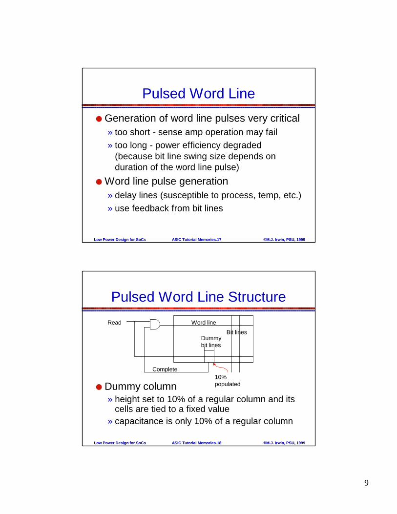
Pulsed Word Line
lGeneration of word line pulses very critical» too short - sense amp operation may fail» too long - power efficiency degraded
(because bit line swing size depends on duration of the word line pulse)
lWord line pulse generation» delay lines (susceptible to process, temp, etc.)» use feedback from bit lines
ASIC Tutorial Memories.ASIC Tutorial Memories.1818Low Power Design for Low Power Design for SoCsSoCs ©©M.J. Irwin, PSU, 1999M.J. Irwin, PSU, 1999
Pulsed Word Line Structure
lDummy column» height set to 10% of a regular column and its
cells are tied to a fixed value» capacitance is only 10% of a regular column
Read Word line
Bit lines
Complete
Dummybit lines
10%populated

10
ASIC Tutorial Memories.ASIC Tutorial Memories.1919Low Power Design for Low Power Design for SoCsSoCs ©©M.J. Irwin, PSU, 1999M.J. Irwin, PSU, 1999
Pulsed Word Line Timing
lDummy bit lines have reached full swing and trigger pulse shut off when regular bit lines reach 10% swing
Read
Complete
Word line
Bit line
Dummy bit line ∆V = Vdd
∆V = 0.1Vdd
ASIC Tutorial Memories.ASIC Tutorial Memories.2020Low Power Design for Low Power Design for SoCsSoCs ©©M.J. Irwin, PSU, 1999M.J. Irwin, PSU, 1999
Bit Line Isolation
sense
Readsense amplifier
bit lines
isolate
sense amplifier outputs
∆V = 0.1Vdd
∆V = Vdd

11
ASIC Tutorial Memories.ASIC Tutorial Memories.2121Low Power Design for Low Power Design for SoCsSoCs ©©M.J. Irwin, PSU, 1999M.J. Irwin, PSU, 1999
Low Power DRAMs
lConventional DRAMs refresh all rows with a fixed single time interval» read/write stalled while refreshing» refresh period -> tref
» refresh rate -> Rref = #rows + tref
» DRAM power = k * (#read/writes + #ref)
lSo have to worry about optimizing refresh operation as well
ASIC Tutorial Memories.ASIC Tutorial Memories.2222Low Power Design for Low Power Design for SoCsSoCs ©©M.J. Irwin, PSU, 1999M.J. Irwin, PSU, 1999
Optimizing RefreshlSelective refresh architecture (SRA)
» add a valid bit to each memory row and only refresh rows with valid bit set
» reduces refresh 5% to 80%
lVariable refresh architecture (VRA)» data retention time of each cell is different» add a refresh period table and refresh counter
to each row and refresh with the appropriate period to each row
» reduces refresh about 75%From From OhsawaOhsawa, 1995, 1995

12
ASIC Tutorial Memories.ASIC Tutorial Memories.2323Low Power Design for Low Power Design for SoCsSoCs ©©M.J. Irwin, PSU, 1999M.J. Irwin, PSU, 1999
Cache PowerlOn-chip I$ and D$ (high speed SRAM)
» DEC 21164a (2.0Vdd, 0.35µ, 400MHz, 30W max)– I/D/L2 of 8/8/96KB and 1/1/? associativity – caches dissipate 25% of the total chip power
» DEC SA-110 (2.0Vdd, 0.35µ, 233MHz, 1W typ)– I/D of 16/16KB and 32/32 associativity (no L2 on-chip)– I$ (D$) dissipate 27% (16%) of the total chip power
l Improving the power efficiency of caches is critical to the overall system power
ASIC Tutorial Memories.ASIC Tutorial Memories.2424Low Power Design for Low Power Design for SoCsSoCs ©©M.J. Irwin, PSU, 1999M.J. Irwin, PSU, 1999
Cache Power Distribution
0
200
400
600
800
1000
1200
1400
1600
1800
ijpeg perl fppp avg
L1 I$L1 D$L2
Pow
er in
mill
iwat
ts
Base Configuration:4-way superscalar32KB DM L1 I$32KB, 4-way SA L1 D$
32B blocks, write back128KB, 4-way SA L2
64B blocks, write back1MB, 8-way SA off-chip L3
128B blocks, write thru
Interconnect widths16B between L1 and L232B between L2 and L364B between L3 and MM
From From GhoshGhosh, 1999, 1999

13
ASIC Tutorial Memories.ASIC Tutorial Memories.2525Low Power Design for Low Power Design for SoCsSoCs ©©M.J. Irwin, PSU, 1999M.J. Irwin, PSU, 1999
Low Power Cache Techniques
lSRAM power reductionlCache block bufferinglCache subbankinglDivided word linelMultidivided module (MDM)lModifications to CAM cell (for FA cache
and FA TLB)
ASIC Tutorial Memories.ASIC Tutorial Memories.2626Low Power Design for Low Power Design for SoCsSoCs ©©M.J. Irwin, PSU, 1999M.J. Irwin, PSU, 1999
Cache Block Buffering
lCheck to see if data desired is in the data output latch from the last cache access (i.e., in the same cache block)
lSaves energy since not accessing tag and data arrays» minimal overhead hardware
lCan maintain performance of normal set associative cache

14
ASIC Tutorial Memories.ASIC Tutorial Memories.2727Low Power Design for Low Power Design for SoCsSoCs ©©M.J. Irwin, PSU, 1999M.J. Irwin, PSU, 1999
Block Buffer Cache Structure
Tag Data
=
Tag Data
=
Address issued by CPU
last_set_#
=
disable sensing
Hit Desired word
ASIC Tutorial Memories.ASIC Tutorial Memories.2828Low Power Design for Low Power Design for SoCsSoCs ©©M.J. Irwin, PSU, 1999M.J. Irwin, PSU, 1999
Block Buffering Performance
0300600900
1200
150018002100240027003000
L1 I$ L1 D$ L2 Total
0 buffers1 buffer2 buffers
Same base configuration4-way superscalar32KB DM L1 I$...
Pow
er in
mill
iwat
ts
From From GhoshGhosh, 1999, 1999

15
ASIC Tutorial Memories.ASIC Tutorial Memories.2929Low Power Design for Low Power Design for SoCsSoCs ©©M.J. Irwin, PSU, 1999M.J. Irwin, PSU, 1999
TagTag
Cache Subbanking
Tag Data
=
Tag Data
=
Address issued by CPU
Hit Desired word
subbank 0
subbank 1
Similar to columnmultiplexing in SRAMs
columns can shareprecharge and sense ampseach subbank has its own decoder
Only read fromone subbank
ASIC Tutorial Memories.ASIC Tutorial Memories.3030Low Power Design for Low Power Design for SoCsSoCs ©©M.J. Irwin, PSU, 1999M.J. Irwin, PSU, 1999
Subbanking Performance
0
600
1200
1800
2400
3000
3600
L1 I$ L1 D$ L2 Total
conv 16Bsubbank 16Bconv 32Bsubbank 32B
Same base configuration4-way superscalar32KB DM L1 I$…
4B subbank width
Pow
er in
mill
iwat
ts
From From GhoshGhosh, 1999, 1999
16
ASIC Tutorial Memories.ASIC Tutorial Memories.3131Low Power Design for Low Power Design for SoCsSoCs ©©M.J. Irwin, PSU, 1999M.J. Irwin, PSU, 1999
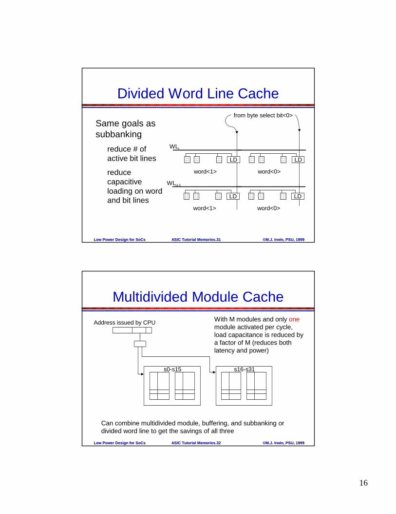
Divided Word Line Cache
LD
WLi+1
LD
word<1> word<0>
from byte select bit<0>
LD
WLi
LD
word<1> word<0>
Same goals as subbanking
reduce # of active bit lines
reduce capacitive loading on word and bit lines
ASIC Tutorial Memories.ASIC Tutorial Memories.3232Low Power Design for Low Power Design for SoCsSoCs ©©M.J. Irwin, PSU, 1999M.J. Irwin, PSU, 1999
Multidivided Module Cache
Address issued by CPU
s0-s15 s16-s31
With M modules and only onemodule activated per cycle,load capacitance is reduced bya factor of M (reduces both latency and power)
Can combine multidivided module, buffering, and subbanking or divided word line to get the savings of all three
17
ASIC Tutorial Memories.ASIC Tutorial Memories.3333Low Power Design for Low Power Design for SoCsSoCs ©©M.J. Irwin, PSU, 1999M.J. Irwin, PSU, 1999
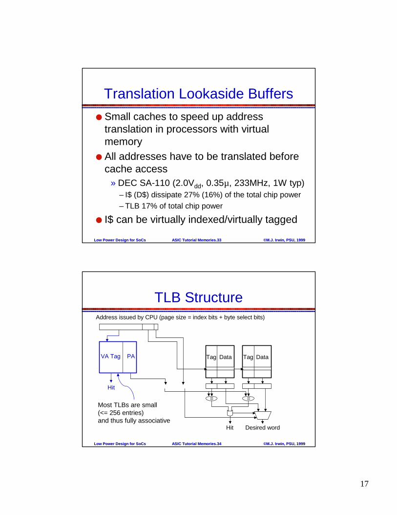
Translation Lookaside BufferslSmall caches to speed up address
translation in processors with virtual memory
lAll addresses have to be translated before cache access
» DEC SA-110 (2.0Vdd, 0.35µ, 233MHz, 1W typ)– I$ (D$) dissipate 27% (16%) of the total chip power– TLB 17% of total chip power
l I$ can be virtually indexed/virtually tagged
ASIC Tutorial Memories.ASIC Tutorial Memories.3434Low Power Design for Low Power Design for SoCsSoCs ©©M.J. Irwin, PSU, 1999M.J. Irwin, PSU, 1999
TLB StructureAddress issued by CPU (page size = index bits + byte select bits)
Tag Data
=
Tag Data
=
Hit Desired word
VA Tag PA
Most TLBs are small(<= 256 entries)and thus fully associative
Hit

18
ASIC Tutorial Memories.ASIC Tutorial Memories.3535Low Power Design for Low Power Design for SoCsSoCs ©©M.J. Irwin, PSU, 1999M.J. Irwin, PSU, 1999
TLB Power
0
10
20
30
40
50
60
70
80
32 64 128 256
DM2 SA4 SA8 SAFA
Pow
er in
mill
iwat
ts
From Juan, 1997From Juan, 1997
ASIC Tutorial Memories.ASIC Tutorial Memories.3636Low Power Design for Low Power Design for SoCsSoCs ©©M.J. Irwin, PSU, 1999M.J. Irwin, PSU, 1999
CAM Design
Read/Write Circuitry
Hit
match<0>
match<1>
match<2>
match<3>
match/write data
WL<0>
WL<1>
WL<2>
WL<3>
precharge/match
match
WLbit bit
word line<0>of data array
19
ASIC Tutorial Memories.ASIC Tutorial Memories.3737Low Power Design for Low Power Design for SoCsSoCs ©©M.J. Irwin, PSU, 1999M.J. Irwin, PSU, 1999
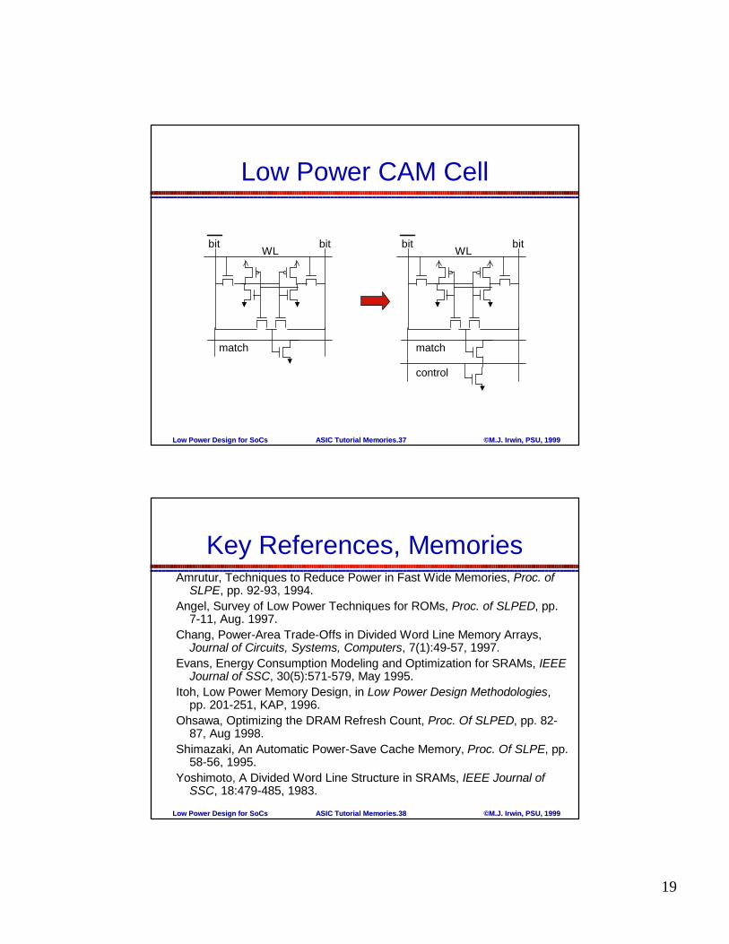
Low Power CAM Cell
match
WLbit bit
control
match
WLbit bit
ASIC Tutorial Memories.ASIC Tutorial Memories.3838Low Power Design for Low Power Design for SoCsSoCs ©©M.J. Irwin, PSU, 1999M.J. Irwin, PSU, 1999
Key References, MemoriesAmrutur, Techniques to Reduce Power in Fast Wide Memories, Proc. of
SLPE, pp. 92-93, 1994.Angel, Survey of Low Power Techniques for ROMs, Proc. of SLPED, pp.
7-11, Aug. 1997.Chang, Power-Area Trade-Offs in Divided Word Line Memory Arrays,
Journal of Circuits, Systems, Computers, 7(1):49-57, 1997.Evans, Energy Consumption Modeling and Optimization for SRAMs, IEEE
Journal of SSC, 30(5):571-579, May 1995.Itoh, Low Power Memory Design, in Low Power Design Methodologies,
pp. 201-251, KAP, 1996.Ohsawa, Optimizing the DRAM Refresh Count, Proc. Of SLPED, pp. 82-
87, Aug 1998.Shimazaki, An Automatic Power-Save Cache Memory, Proc. Of SLPE, pp.
58-56, 1995.Yoshimoto, A Divided Word Line Structure in SRAMs, IEEE Journal of
SSC, 18:479-485, 1983.
20
ASIC Tutorial Memories.ASIC Tutorial Memories.3939Low Power Design for Low Power Design for SoCsSoCs ©©M.J. Irwin, PSU, 1999M.J. Irwin, PSU, 1999
Key References, CachesGhose, A 0.5 micron Cache and Its Low Power Variants, Proc. of
ISLPED, pp. 70-75, 1999.Juan, Reducing TLB Power Requirements, Proc. of ISLPED, pp. 196-
201, Aug 1997.Kin, The Filter Cache: An Energy-Efficient Memory Structure, Proc. of
MICRO, pp. 184-193, Dec. 1997.Ko, Energy Optimization of Multilevel Cache Architectures, IEEE Trans.
On VLSI Systems, 6(2):299-308, June 1998.Panwar, Reducing the Frequency of Tag Compares for Low Power I$
Designs, Proc. of ISLPD, pp. 57-62, 1995.Shimazaki, An Automatic Power-Save Cache Memory, Proc. of SLPE,
pp. 58-59, 1995.Su, Cache Design Tradeoffs for Power and Performance Optimization,
Proc. of ISLPD, pp. 63-68, 1995.