
Power 'n Motors
36
Power 'n Motors Critical aspects in power applications design, proper component selection & experimental results
Transcript of Power 'n Motors
Power 'n Motors
Critical aspects in power applications design, proper component selection & experimental results
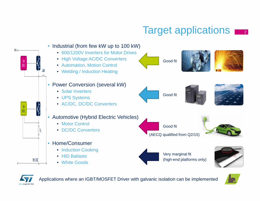
• Industrial (from few kW up to 100 kW)• 600/1200V Inverters for Motor Drives• High Voltage AC/DC Converters• Automation, Motion Control• Welding / Induction Heating
• Power Conversion (several kW)• Solar Inverters• UPS Systems• AC/DC, DC/DC Converters
• Automotive (Hybrid Electric Vehicles)• Motor Control• DC/DC Converters
• Home/Consumer• Induction Cooking• HID Ballasts• White Goods
Target applications 2
Very marginal fit(high-end platforms only)
Good fit
Applications where an IGBT/MOSFET Driver with galvanic isolation can be implemented
Good fit
Good fit
(AECQ qualified from Q2/15)
Introducing STGAP1S
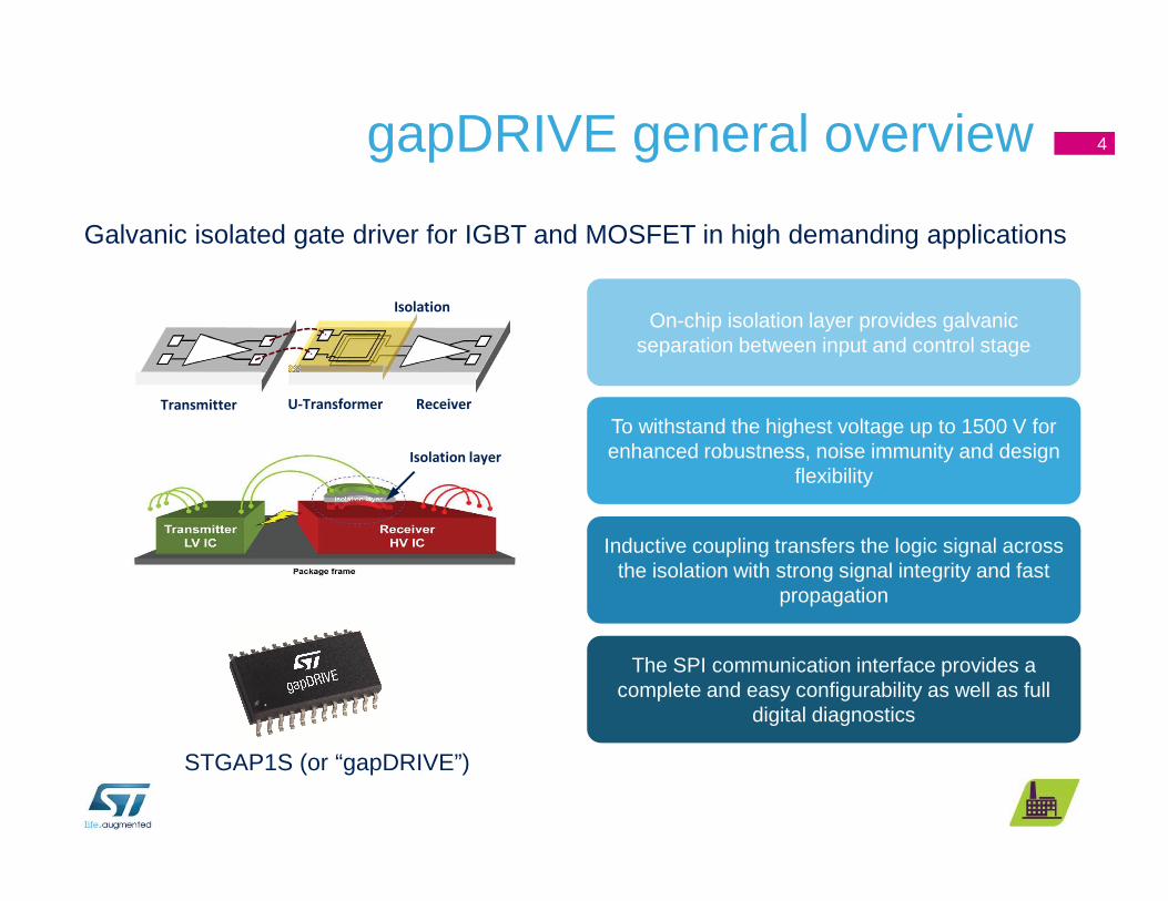
gapDRIVE general overview 4
Galvanic isolated gate driver for IGBT and MOSFET in high demanding applications
Transmitter U-Transformer Receiver
Isolation
To withstand the highest voltage up to 1500 V for enhanced robustness, noise immunity and design
flexibility
Inductive coupling transfers the logic signal across the isolation with strong signal integrity and fast
propagation
The SPI communication interface provides a complete and easy configurability as well as full
digital diagnostics
On-chip isolation layer provides galvanic separation between input and control stage
STGAP1S (or “gapDRIVE”)
Isolation layer

What kind of insulation and why 5
• Power applications often require galvanic isolation due to:• High side driving (functional isolation)
• Safety (galvanic isolation)
• Noise minimization (interference between LV/Logic part with HV/Power stage)
• Integrated insulation guarantees cost and space savings• Optical isolation
• Ageing of LED and transparent insulator lead to variation of propagation delay and reliability issues
• Limited dV/dt capability
• Capacitive coupling• Prone to electrical field disturbance, therefore not well suited for high power applications
• Limited dV/dt capability as for the optical isolation
• Inductive coupling• High immunity to magnetic field thanks to coil topo logy
• Very good dV/dt capability (>50 V/ns)
• Transfer of logic signals across a 4 kV galvanic iso lation
(maximum surge insulation voltage)
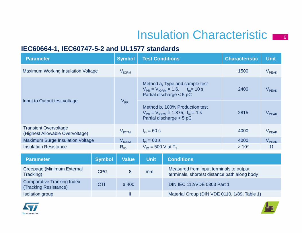
Insulation Characteristic 6
IEC60664-1, IEC60747-5-2 and UL1577 standardsParameter Symbol Test Conditions Characteristic Unit
Maximum Working Insulation Voltage VIORM 1500 VPEAK
Input to Output test voltage VPR
Method a, Type and sample testVPR = VIORM × 1.6, tm= 10 sPartial discharge < 5 pC
2400 VPEAK
Method b, 100% Production testVPR = VIORM × 1.875, tm = 1 sPartial discharge < 5 pC
2815 VPEAK
Transient Overvoltage(Highest Allowable Overvoltage)
VIOTM tini = 60 s 4000 VPEAK
Maximum Surge Insulation Voltage VIOSM tini = 60 s 4000 VPEAK
Insulation Resistance RIO VIO = 500 V at TS > 109 Ω
Parameter Symbol Value Unit Conditions
Creepage (Minimum External Tracking)
CPG 8 mmMeasured from input terminals to output terminals, shortest distance path along body
Comparative Tracking Index(Tracking Resistance)
CTI ≥ 400 DIN IEC 112/VDE 0303 Part 1
Isolation group II Material Group (DIN VDE 0110, 1/89, Table 1)
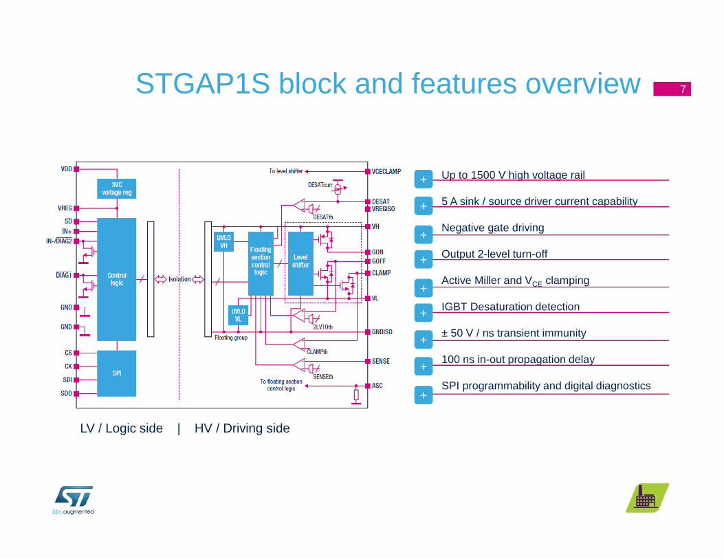
STGAP1S block and features overview
Up to 1500 V high voltage rail
5 A sink / source driver current capability
Negative gate driving
Output 2-level turn-off
Active Miller and VCE clamping
IGBT Desaturation detection
± 50 V / ns transient immunity
100 ns in-out propagation delay
SPI programmability and digital diagnostics
+
+
+
+
+
+
+
+
+
7
LV / Logic side | HV / Driving side
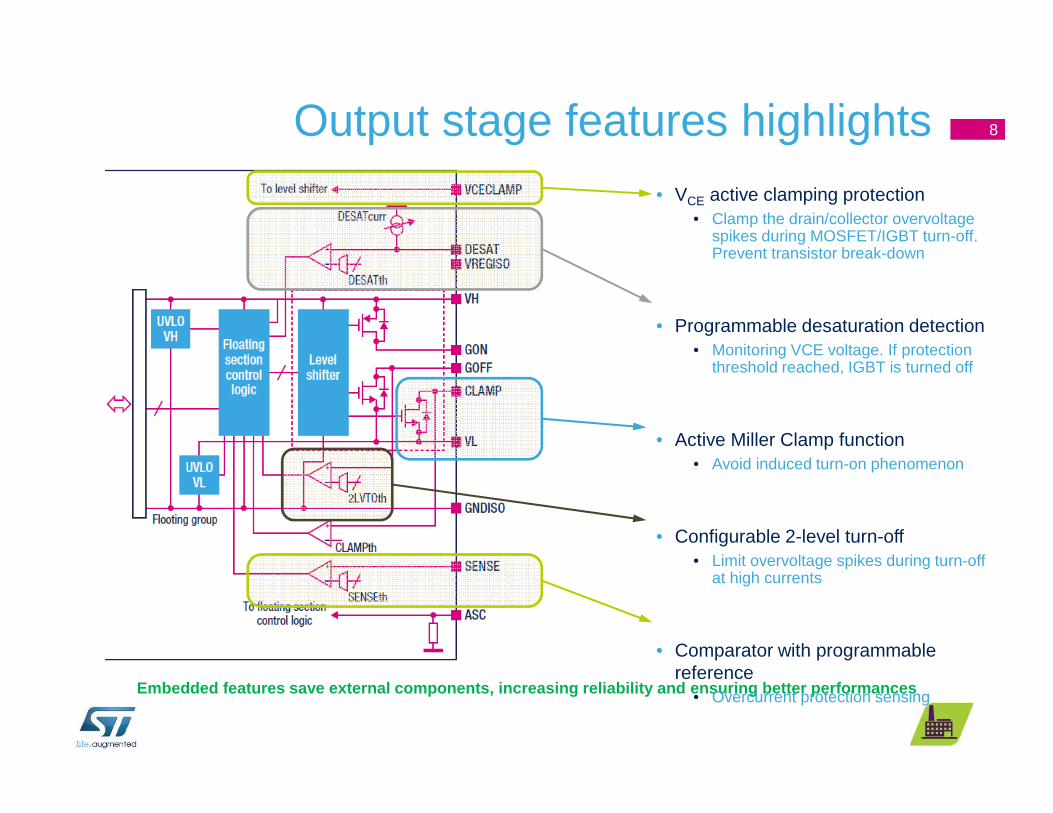
Output stage features highlights 8
Embedded features save external components, increas ing reliability and ensuring better performances
• VCE active clamping protection• Clamp the drain/collector overvoltage
spikes during MOSFET/IGBT turn-off. Prevent transistor break-down
• Programmable desaturation detection • Monitoring VCE voltage. If protection
threshold reached, IGBT is turned off
• Active Miller Clamp function• Avoid induced turn-on phenomenon
• Configurable 2-level turn-off• Limit overvoltage spikes during turn-off
at high currents
• Comparator with programmable reference
• Overcurrent protection sensing

Desaturation detection for OCP 9
• In case the external IGBT desaturates, it may fail due excessive power dissipation: DESATuration protection monitors the VCE voltage and turns the IGBT off if a threshold voltage is reached
• At IGBT turn-on the protection’s intervention is delayed for a fixed time called blanking time so to allow the IGBT to reach the saturation condition
• Fault is transmitted to the fault registers in the low-voltage section. Event signaling to uC via DIAG pins is optional
• Both desaturation threshold and blanking current programmable via SPI• Blanking current up to 1 mA allows better noise filtering without increasing blanking time
DESAT_Th:3 …10 V in 1 V steps
DESAT_Cur :250 µA, 500 µA, 750 µA, 1 mA
Default Configuration: 7 V, 250 µA
Capacitor Discharge Capability: 35 mA
2 Level Turn-Off in gapDRIVE 10
• 2LTO can be programmed to occur:• At each cycle (like in TD350)
• Only after a DESAT or Over Current Event No need of the turn-on delay to avoid duty-cycle distortion
No gate voltage reduction during t2LTO in normal conditions
No minimum on-time required
• Never (disabled)
• Both 2LTO voltage and duration are programmable via SPI• V2LTO: 16 values between 7 V and 14.5 V
• t2LTO: 16 values between 750 ns and 5.5 us
• 2LTO offers advantages vs. Soft Turn-off since it only slows down the turn-off speed for the minimum necessary time to avoid over-voltages, thus limiting the duration of the high-voltage high-current overstressing condition
• 2LTO protects power switches from VCE overvoltage spikes during turn-off in case of overcurrent conditions
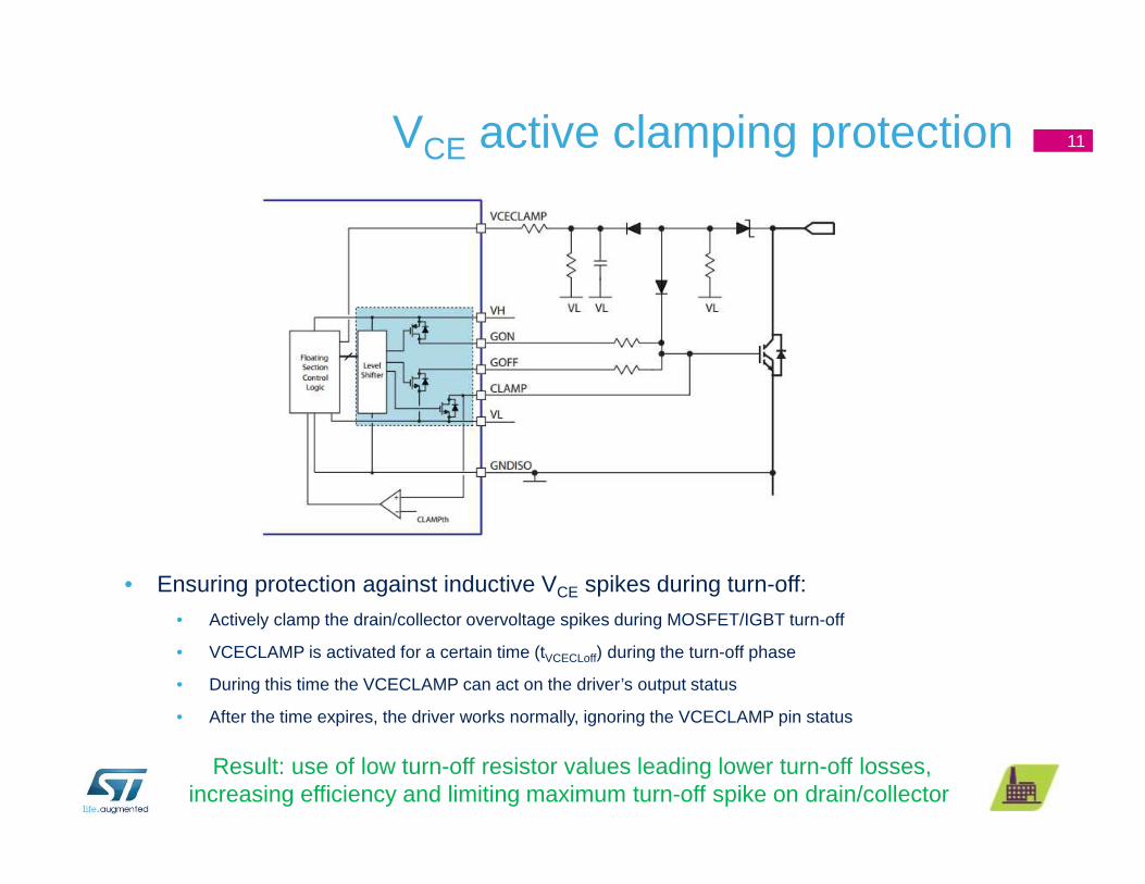
VCE active clamping protection 11
• Ensuring protection against inductive VCE spikes during turn-off:
• Actively clamp the drain/collector overvoltage spikes during MOSFET/IGBT turn-off
• VCECLAMP is activated for a certain time (tVCECLoff) during the turn-off phase
• During this time the VCECLAMP can act on the driver’s output status
• After the time expires, the driver works normally, ignoring the VCECLAMP pin status
Result: use of low turn-off resistor values leading lower turn-off losses, increasing efficiency and limiting maximum turn-off spike on drain/collector
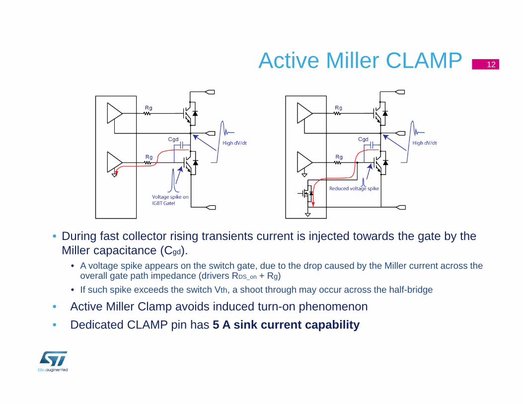
Active Miller CLAMP 12
• During fast collector rising transients current is injected towards the gate by the Miller capacitance (Cgd).
• A voltage spike appears on the switch gate, due to the drop caused by the Miller current across the overall gate path impedance (drivers RDS_on + Rg)
• If such spike exceeds the switch Vth, a shoot through may occur across the half-bridge
• Active Miller Clamp avoids induced turn-on phenomenon
• Dedicated CLAMP pin has 5 A sink current capability
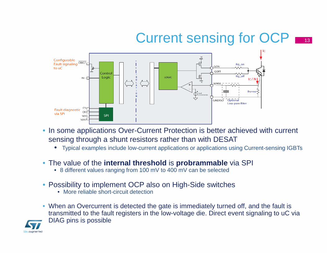
Current sensing for OCP 13
• In some applications Over-Current Protection is better achieved with current sensing through a shunt resistors rather than with DESAT
• Typical examples include low-current applications or applications using Current-sensing IGBTs
• The value of the internal threshold is probrammable via SPI• 8 different values ranging from 100 mV to 400 mV can be selected
• Possibility to implement OCP also on High-Side switches• More reliable short-circuit detection
• When an Overcurrent is detected the gate is immediately turned off, and the fault is transmitted to the fault registers in the low-voltage die. Direct event signaling to uC via DIAG pins is possible
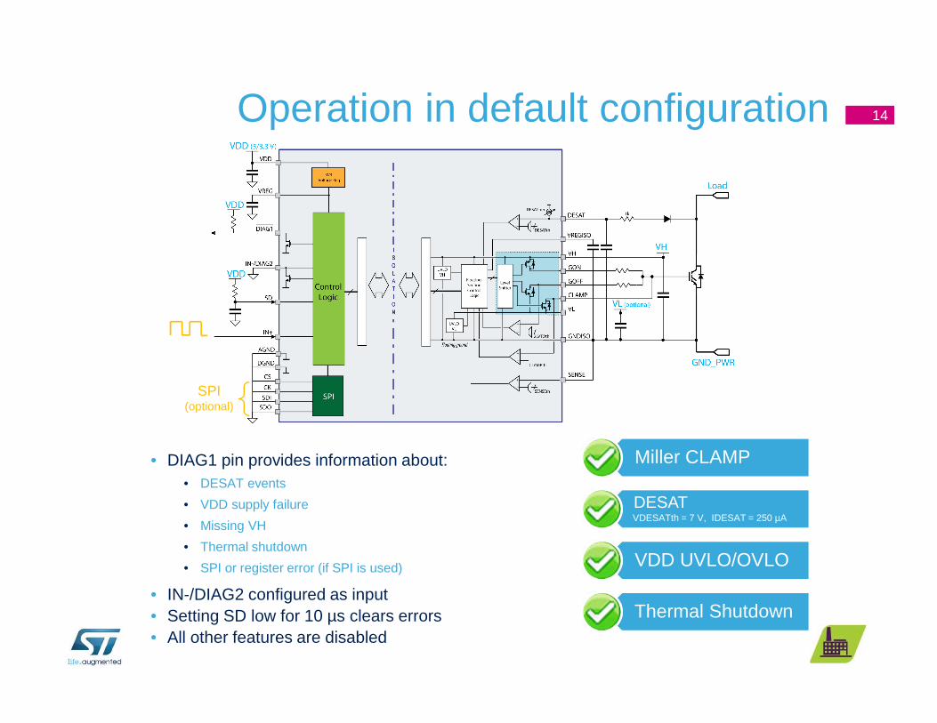
Operation in default configuration 14
SPI (optional)
Miller CLAMP
DESATVDESATth = 7 V, IDESAT = 250 µA
VDD UVLO/OVLO
Thermal Shutdown
• DIAG1 pin provides information about:• DESAT events
• VDD supply failure
• Missing VH
• Thermal shutdown
• SPI or register error (if SPI is used)
• IN-/DIAG2 configured as input• Setting SD low for 10 µs clears errors• All other features are disabled
14
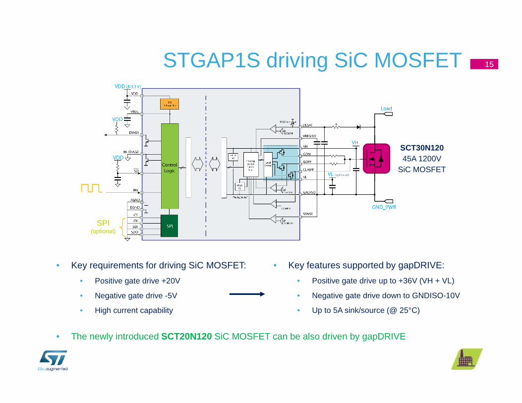
STGAP1S driving SiC MOSFET 15
SPI (optional)
SCT30N12045A 1200V
SiC MOSFET
• Key requirements for driving SiC MOSFET:
• Positive gate drive +20V
• Negative gate drive -5V
• High current capability
• Key features supported by gapDRIVE:
• Positive gate drive up to +36V (VH + VL)
• Negative gate drive down to GNDISO-10V
• Up to 5A sink/source (@ 25°C)
• The newly introduced SCT20N120 SiC MOSFET can be also driven by gapDRIVE

STGAP1S basic configuration• If VDD=3.3V required:
• Short pin VREG (6) with VDD (7)
• If SPI not used
• Connect all SPI lines to GND SDO, SDI, CS and CK
• SD pin start-up “network”
• SD pin needs to stay at least 10us at logic low after power-on to leave “safe state”
• Pull-up pin SD (11) to VDD with resistor xx kΩ together with coupling to GND with 10nF capacitor
• If driven with +input signal (power switch ON with logic “1”)
• Input logic signal tied on IN+ (9); pin IN-/DIAG2 (8) to GND
• If drive with -input signal (power switch ON with logic “0”)
• Input logic signal tied on IN-/DIAG2 (8); pin IN+ (9) to VDD
• If DESAT protection activated, pin DIAG1 is latched to GND
• If DESAT protection unused (default VDESATth=7V; IDESAT=250µA)
• Connect DESAT (18) pin to GNDISO
16
Basic configuration helps designers to bridge the time to STGAP2S (gapLITE)

Half-bridge connection example 17
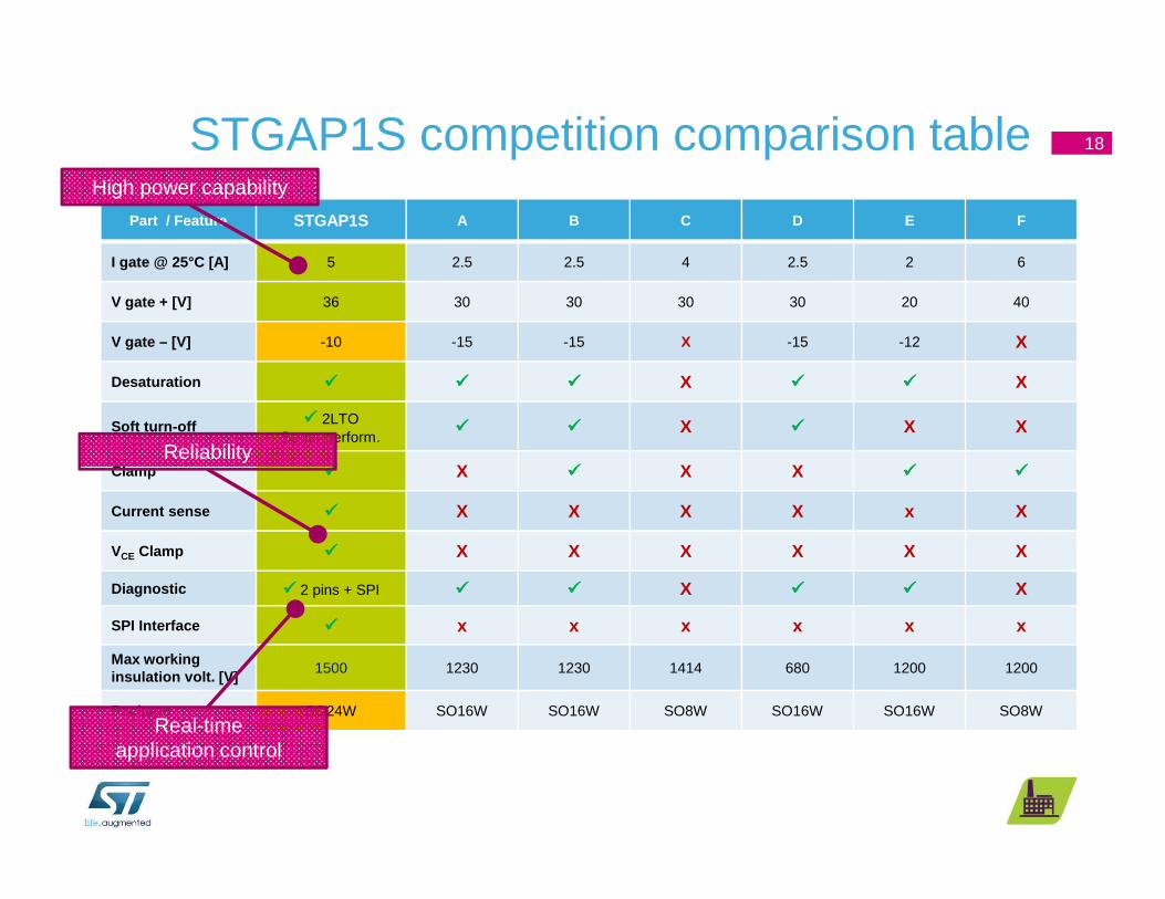
STGAP1S competition comparison table
Part / Feature STGAP1S A B C D E F
I gate @ 25°C [A] 5 2.5 2.5 4 2.5 2 6
V gate + [V] 36 30 30 30 30 20 40
V gate – [V] -10 -15 -15 X -15 -12 X
Desaturation X X
Soft turn-off 2LTOBetter perform.
X X X
Clamp X X X
Current sense X X X X x X
VCE Clamp X X X X X X
Diagnostic 2 pins + SPI X X
SPI Interface x x x x x x
Max working insulation volt. [V]
1500 1230 1230 1414 680 1200 1200
Package SO24W SO16W SO16W SO8W SO16W SO16W SO8W
Reliability
High power capability
Real-timeapplication control
18
Main application topologies
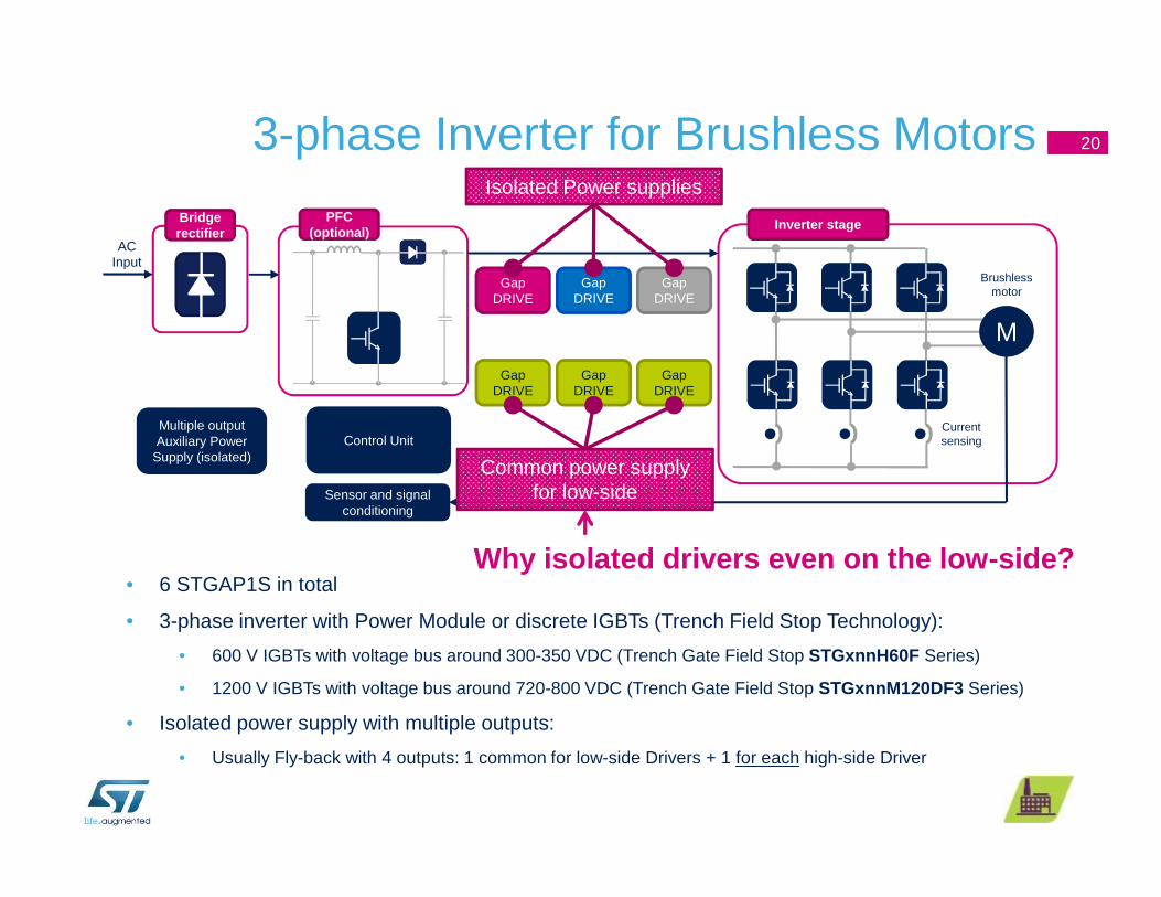
3-phase Inverter for Brushless Motors 2020
PFC(optional)
Bridge rectifier
Inverter stage
Control UnitMultiple output Auxiliary Power
Supply (isolated)
ACInput
Brushless motor
20
M
Sensor and signal conditioning
GapDRIVE
Current sensing
• 6 STGAP1S in total
• 3-phase inverter with Power Module or discrete IGBTs (Trench Field Stop Technology):
• 600 V IGBTs with voltage bus around 300-350 VDC (Trench Gate Field Stop STGxnnH60F Series)
• 1200 V IGBTs with voltage bus around 720-800 VDC (Trench Gate Field Stop STGxnnM120DF3 Series)
• Isolated power supply with multiple outputs:
• Usually Fly-back with 4 outputs: 1 common for low-side Drivers + 1 for each high-side Driver
GapDRIVE
GapDRIVE
GapDRIVE
GapDRIVE
GapDRIVE
Isolated Power supplies
Common power supply for low-side
Why isolated drivers even on the low-side?

Welding: Full-Bridge topology 21
Output rectifier
DC Output for steel welding
Secondaryinverter
PFC(optional)
Bridge rectifier
Control Unit
Multiple output Auxiliary
power supply (isolated)
ACInput
Primaryinverter
AC Output for aluminum
welding
21
GapDRIVE
GapDRIVE
GapDRIVE
GapDRIVE
• 8 gapDRIVE in total (4 + 4)
• Welding, full-bridge topology for single and phase-to-phase inverters with discrete IGBTs:
• 600 V IGBTs with voltage bus around 300-350 VDC
• 1200 V IGBT with voltage bus around 720-800 VDC
• Isolated power supply with multiple outputs:
• Usually Fly-back with 3 outputs: 1 common for low-side Drivers + 1 for each high-side Driver
• Secondary inverter needs additional isolated power supply
GapDRIVE
GapDRIVE
GapDRIVE
GapDRIVE

Solar Full-Bridge Mixed Frequency Converter 2222
Output filter
ACOutput
Multiple output Auxiliary
power supply (isolated)
Control Unit
Full-bridge mixed freq.Boost
converter
PV input
GapDRIVE
GapDRIVE
GapDRIVE
GapDRIVE
• 4 gapDRIVE in total
• Solar full-bridge mixed frequency converter:
• 600 V IGBTs with voltage bus around 300-350 VDC
• 1200 V IGBT with voltage bus around 720-800 VDC
• Isolated power supply with multiple outputs:
• Usually Fly-back with 3 outputs: 1 common for low-side Drivers + 1 for each high-side Driver

Connecting STGAP1S3-phase Motor Control example
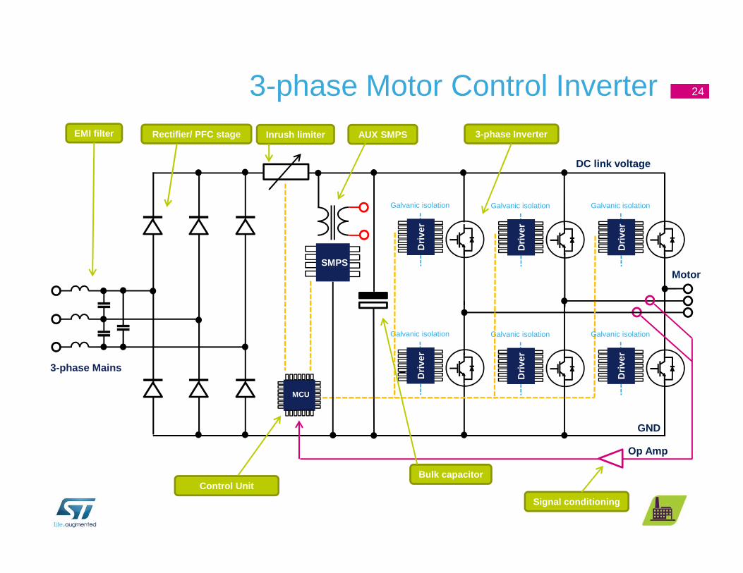
3-phase Motor Control Inverter 24
MCU
SMPS
3-phase Inverter
Control Unit
Motor
DC link voltage
GND
Driv
er
Galvanic isolation
Driv
er
Galvanic isolation
Driv
er
Galvanic isolation
Driv
er
Galvanic isolation
Driv
er
Galvanic isolation
Driv
er
Galvanic isolation
3-phase Mains
Inrush limiterRectifier/ PFC stageEMI filter AUX SMPS
Signal conditioning
Op Amp
Bulk capacitor
gapDRIVE in a 3-phase inverter 25
ST
GA
P1S
ST
GA
P1S
ST
GA
P1S
ST
GA
P1S
ST
GA
P1S
ST
GA
P1S
ControlUnit
SMPS
4) +15V/ GND/ -10V
5) +15V/ GND/ -10V
3) +15V/ GND/ -10V
Galvanic isolated branches for each high side drive rs
SPI
SPI Interface (daisy chain)
Driving Signals
PWM Driving signals IN+/ IN-
Motor
DC link voltage
GND
2) +15V/ GND/ -10V
Galvanic isolated branch common for all low side dr ivers
1) +5V (3.3V)
Vcc supply for primary logic and MCU
Galvanic isolationSupply Voltage
Multiple OutputAuxiliary
Power Supply(Isolated)
Galvanic isolationGalvanic isolation
gapDRIVE in a 3-phase inverter 26
ST
GA
P1S
ST
GA
P1S
ST
GA
P1S
ST
GA
P1S
ST
GA
P1S
ST
GA
P1S
SPI
SPI Interface (daisy chain)
Driving Signals
PWM Driving signals IN+/ IN-
Motor
DC link voltage
GND
1) +5V (3.3V)
Vcc supply for primary logic and MCU
2) +15V/ GND/-10V
Galvanic isolated branch common for all low side dr ivers
Galvanic isolated DC/DC converters – separated branc h for each HS drivers
+15V/ GND/ -10V
DC/DC DC/DC DC/DC
+15V/ GND/ -10V +15V/ GND/ -10V
Supply Voltage
ControlUnit
SMPS
Multiple OutputAuxiliary
Power Supply(Isolated) Galvanic isolationGalvanic isolationGalvanic isolation
Application test at Czech UniversityDriving a 60 kW inductive load

Cooperation with Czech University in Prague
• Test capabilities in real environment:
• Test of STGAP1S with IGBT module and inductive load:
• Measure the performance of driving capability
• Test set-up, key features:
• 1200 V, 150 A IGBT power module
• 5 kHz switching frequency, 50% duty-cycle
• 2x modified EVALgapDRIVE evaluation boards
• High C capacitors (2200 µF, 450 VDC each), for DC-BUS
• HV power supply 720 VDC, 80 A, ~60kW total power
• LV isolated power supply 5 V and 15 V DC
• About 60kW inductive load for motor simulation
• Power System designed by ST
• Generator and load provided by Czech Technical University
Test set-up, Laboratory of Motor Driving, CVUT
Load inductor (100kg), load resistor (wall closet)
28
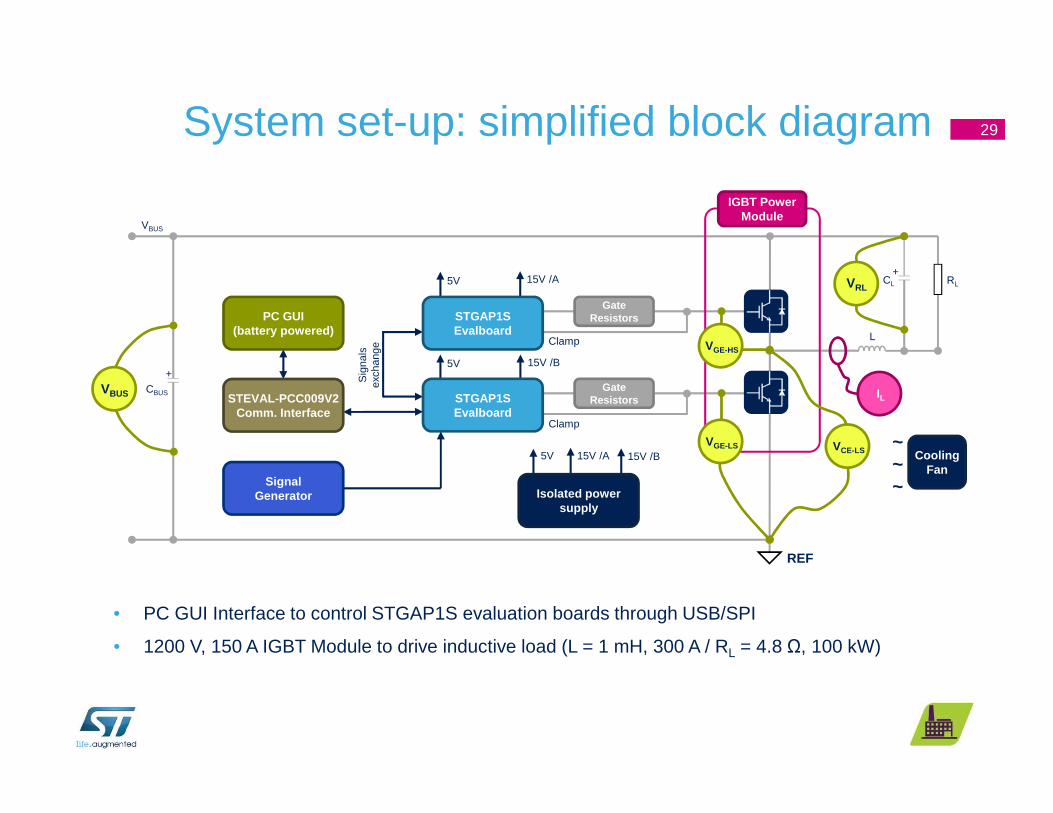
29System set-up: simplified block diagram
• PC GUI Interface to control STGAP1S evaluation boards through USB/SPI
• 1200 V, 150 A IGBT Module to drive inductive load (L = 1 mH, 300 A / RL = 4.8 Ω, 100 kW)
15V /A
GateResistors
IGBT PowerModule
STGAP1SEvalboard
Clamp
GateResistorsSTGAP1S
EvalboardClamp
15V /B
5V
5VS
igna
lsex
chan
ge
+
VBUS
+
L
RLCL
CBUS
PC GUI(battery powered)
STEVAL-PCC009V2Comm. Interface
SignalGenerator
VBUS
VRL
VGE-LS
VGE-HS
VCE-LS
IL
REF
15V /B5V 15V /A
Isolated powersupply
CoolingFan
~~~
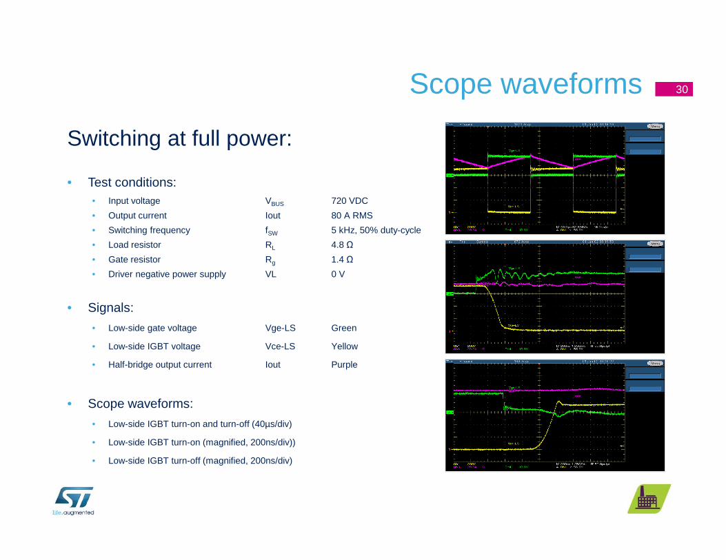
30Scope waveforms
Switching at full power:
• Test conditions:• Input voltage VBUS 720 VDC
• Output current Iout 80 A RMS
• Switching frequency fSW 5 kHz, 50% duty-cycle
• Load resistor RL 4.8 Ω
• Gate resistor Rg 1.4 Ω
• Driver negative power supply VL 0 V
• Signals:
• Low-side gate voltage Vge-LS Green
• Low-side IGBT voltage Vce-LS Yellow
• Half-bridge output current Iout Purple
• Scope waveforms:
• Low-side IGBT turn-on and turn-off (40µs/div)
• Low-side IGBT turn-on (magnified, 200ns/div))
• Low-side IGBT turn-off (magnified, 200ns/div)
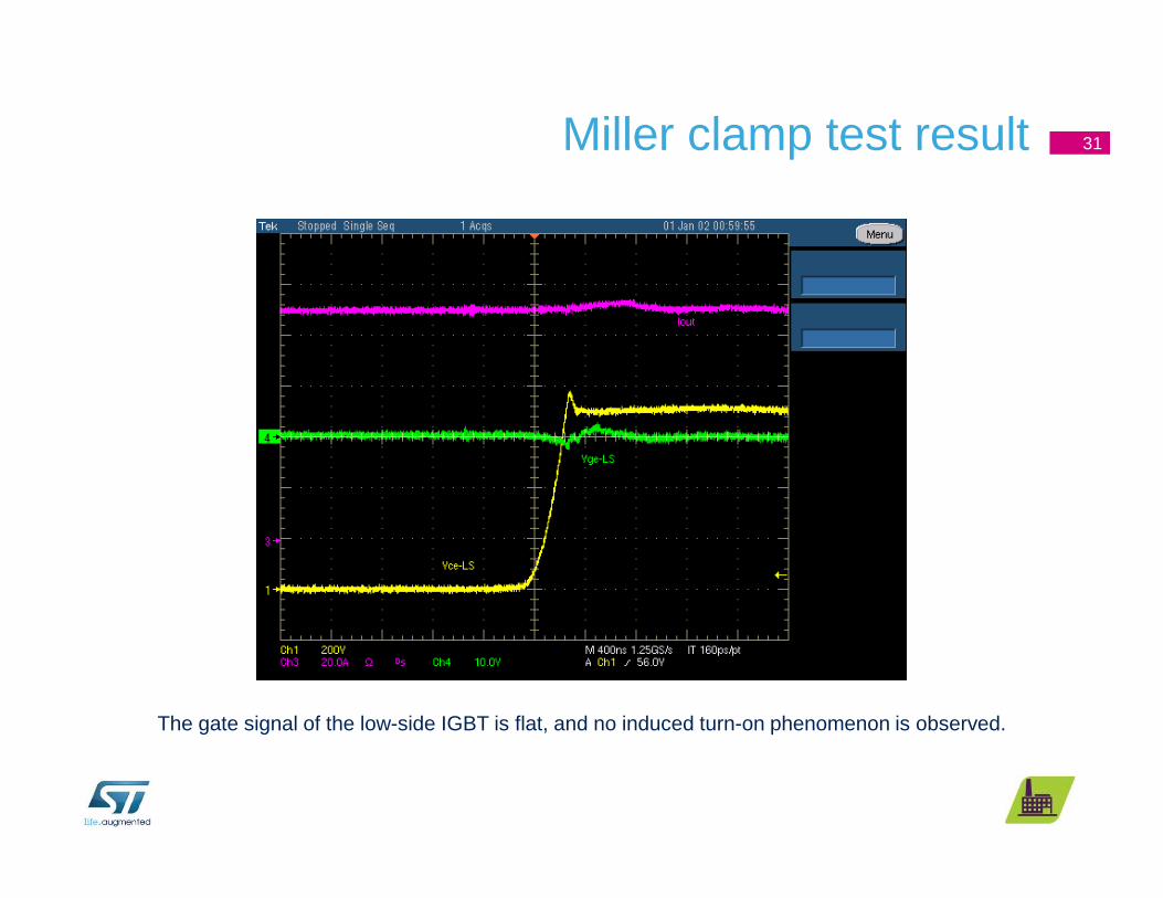
31Miller clamp test result
The gate signal of the low-side IGBT is flat, and no induced turn-on phenomenon is observed.

32Thermal camera snapshots
IGBT Module
High-side and Low-side drivers
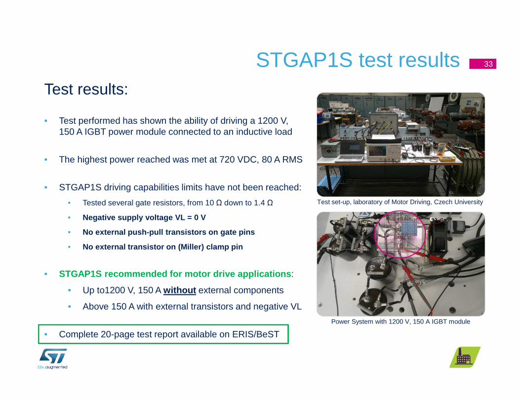
33STGAP1S test resultsTest results:
• Test performed has shown the ability of driving a 1200 V, 150 A IGBT power module connected to an inductive load
• The highest power reached was met at 720 VDC, 80 A RMS
• STGAP1S driving capabilities limits have not been reached:
• Tested several gate resistors, from 10 Ω down to 1.4 Ω
• Negative supply voltage VL = 0 V
• No external push-pull transistors on gate pins
• No external transistor on (Miller) clamp pin
• STGAP1S recommended for motor drive applications :
• Up to1200 V, 150 A without external components
• Above 150 A with external transistors and negative VL
• Complete 20-page test report available on ERIS/BeST
Test set-up, laboratory of Motor Driving, Czech University
Power System with 1200 V, 150 A IGBT module

Evaluation boards & toolsIPD technical support

Documentation, Tools and Technical Support
• How to ease time to market:
• Documentation:
• Main page on st.com: STGAP1S
• Technical report: testing gapDRIVE capabilities (ERIS/BeST)
• Evaluation boards:
• Plug-and-play demonstration board: EVALSTGAP1S
• PC Communication Interface: STEVAL-PCC009V2
• Graphical User Interface (GUI):
• Available on the web: STSW-STGAP001
• Technical Support provided by Prague’s Team:
• Send your request to: [email protected]
35
STEVAL-PCC009V2 Communication Interface
STGAP1S Graphic User Interface (GUI)
EVALSTGAP1S Demonstration Board

www.st.com
www.st.com/gapdrive