Power Loss Estimation for PWM and Soft-switching Inverter ... · Power Loss Estimation for PWM and...
6
Power Loss Estimation for PWM and Soft-switching Inverter using RDCLI Sushant kumar Pattnaik and K. K. Mahapatra Abstract--- The inspiration for the use of the resonant inverter shoots from an aspiration to minimise the switching losses in the inverter devices. This paper portrays an exhaustive study on losses in the resonant DC link inverter. Equations for accessing the diverse losses in the resonant DC link inverter and a corresponding hard switching inverter are developed. Based on these equations, a design optimization is executed for the DC link inverter to attain the optimum standards of the link components. Finally, an evaluation of the losses in the resonant inverter and the hard switching inverter is presented. Index Terms— Power Loss, PWM Inverter, Resonant DC Link Inverter, Soft-Switched Inverter. I. INTRODUCTION PWM (Pulse Width Modulation) Inverters and Soft- Switching Inverters (SSI) are used in power electronics literature extensively. Both classes of inverters find applications in several domains. Soft-Switching Inverters are developed in recent times primarily to reduce switching losses. Both PWM and SSI inverters provide a different advantages vis-à-vis disadvantages which are documented in the literature [1]-[9]. In this paper an attempt is made to evaluate losses in both types of inverters. This would facilitate for optimum design of link components in the Resonant DC Link Inverter (RDCLI). Here a detailed analysis of the losses in the resonant DC link inverter is made. Equations for estimating the various losses in the resonant DC link inverter and an equivalent hard switching inverter are developed. Based on these equations, a design optimization is performed for the resonant DC link inverter to find the optimum values of the link components. Finally, a comparison of the losses in the resonant inverter and hard switching inverter is made. The rest of this paper is compiled as follows. Various losses associated with the hard switching inverter is discussed in section II. Losses due to Soft-switching Inverters are discussed is presented in section III. Resonant Inductor loss is briefed in section IV. In section V System Optimization is made and Graphs & Results are discussed. Finally a conclusion is drawn in section VI. Manuscript received on December 1, 2009. This work was supported by Ministry of Communication and Information Technology, Government of India. Sushant Kumar Pattnaik is a Research Scholar at ECE Department, at National Institute of Technology, Rourkela, INDIA. (Phone: +91- 9437082906; e-mail: suhsantpattnaik@ gmail.com). Kamala Kanta Mahapatra is Professor at ECE Department, at National Institute of Technology, Rourkela, INDIA. (Phone: 0661-2462454; e-mail: kmaha2@ gmail.com). II. LOSSES IN THE HARD SWITCHING INVERTER The key power losses, in the hard switching inverter, are the conduction and switching losses in the inverter devices. Occurrence of the conduction losses is due to the declining voltage across the device as well as the current flow through the device striking in chorus. Switching losses are sustained by the concurrent occurrence of voltage and current on the device while switching. Evaluation of these losses can be done using simplified device models. A. Conduction Losses To evaluate conduction loss, the device is simplified as a constant voltage drop in series with a linear resistor. For both IGBTs and diodes, this simplified model is appropriate. The expression for the on-state voltage of an IGBT and a diode is shown in Equations 1.1 and 1.2, respectively. ce q q q V V I R = + ⋅ (1. 1) ak d d d V V I R = + ⋅ (1. 2) I q and I d denotes the current flowing through the IGBT and diode, respectively. V ce and V ak denote the voltage across the IGBT and Diode. The parameters, V q , R q , V d , and R d can be extracted from data sheets. Powers dissipated in a component with a constant voltage drop correspond to the average current times the voltage drop. The rms current squared times the resistance signifies the power dissipated in a resistor. To ease the calculation of the IGBT and diode currents, the load current is assumed to be sinusoidal. Calculating the average and rms currents of the IGBT and diode in an inverter (given sinusoidal pulse width modulation), using Equations 1.3 to 1.6 [6]. 0 q cos 1 I (avg) = I ( )[ ] 2 8 a m pk φ π + (1.3) 0 q cos 1 I (rms) = I ( ) 8 3 a m pk φ π + (1.4) 0 d cos 1 I (avg) = I ( )[ ] 2 8 a m pk φ π − (1. 5) 0 d cos 1 I (rms) = I ( ) 8 3 a m pk φ π − (1.6) Where I 0 (pk) denotes the peak load current, denotes the power factor angle, and m a denotes the modulation index. With the simplified models, the conduction losses in the
Transcript of Power Loss Estimation for PWM and Soft-switching Inverter ... · Power Loss Estimation for PWM and...
Power Loss Estimation for PWM and Soft-switching Inverter using RDCLI
Sushant kumar Pattnaik and K. K. Mahapatra
Abstract--- The inspiration for the use of the resonant inverter shoots from an aspiration to minimise the switching losses in the inverter devices. This paper portrays an exhaustive study on losses in the resonant DC link inverter. Equations for accessing the diverse losses in the resonant DC link inverter and a corresponding hard switching inverter are developed. Based on these equations, a design optimization is executed for the DC link inverter to attain the optimum standards of the link components. Finally, an evaluation of the losses in the resonant inverter and the hard switching inverter is presented.
Index Terms— Power Loss, PWM Inverter, Resonant DC
Link Inverter, Soft-Switched Inverter.
I. INTRODUCTION
PWM (Pulse Width Modulation) Inverters and Soft-
Switching Inverters (SSI) are used in power electronics literature extensively. Both classes of inverters find applications in several domains. Soft-Switching Inverters are developed in recent times primarily to reduce switching losses. Both PWM and SSI inverters provide a different advantages vis-à-vis disadvantages which are documented in the literature [1]-[9]. In this paper an attempt is made to evaluate losses in both types of inverters. This would facilitate for optimum design of link components in the Resonant DC Link Inverter (RDCLI). Here a detailed analysis of the losses in the resonant DC link inverter is made. Equations for estimating the various losses in the resonant DC link inverter and an equivalent hard switching inverter are developed. Based on these equations, a design optimization is performed for the resonant DC link inverter to find the optimum values of the link components. Finally, a comparison of the losses in the resonant inverter and hard switching inverter is made.
The rest of this paper is compiled as follows. Various losses associated with the hard switching inverter is discussed in section II. Losses due to Soft-switching Inverters are discussed is presented in section III. Resonant Inductor loss is briefed in section IV. In section V System Optimization is made and Graphs & Results are discussed. Finally a conclusion is drawn in section VI.
Manuscript received on December 1, 2009. This work was supported by
Ministry of Communication and Information Technology, Government of India.
Sushant Kumar Pattnaik is a Research Scholar at ECE Department, at
National Institute of Technology, Rourkela, INDIA. (Phone: +91-9437082906; e-mail: suhsantpattnaik@ gmail.com).
Kamala Kanta Mahapatra is Professor at ECE Department, at National Institute of Technology, Rourkela, INDIA. (Phone: 0661-2462454; e-mail: kmaha2@ gmail.com).
II. LOSSES IN THE HARD SWITCHING INVERTER
The key power losses, in the hard switching inverter, are the conduction and switching losses in the inverter devices. Occurrence of the conduction losses is due to the declining voltage across the device as well as the current flow through the device striking in chorus. Switching losses are sustained by the concurrent occurrence of voltage and current on the device while switching. Evaluation of these losses can be done using simplified device models.
A. Conduction Losses
To evaluate conduction loss, the device is simplified as a constant voltage drop in series with a linear resistor. For both IGBTs and diodes, this simplified model is appropriate. The expression for the on-state voltage of an IGBT and a diode is shown in Equations 1.1 and 1.2, respectively.
c e q q qV V I R= + ⋅
(1. 1)
a k d d dV V I R= + ⋅ (1. 2)
Iq and Id denotes the current flowing through the IGBT
and diode, respectively. Vce and Vak denote the voltage across the IGBT and Diode. The parameters, Vq, Rq, Vd, and Rd can be extracted from data sheets. Powers dissipated in a component with a constant voltage drop correspond to the average current times the voltage drop. The rms current squared times the resistance signifies the power dissipated in a resistor. To ease the calculation of the IGBT and diode currents, the load current is assumed to be sinusoidal. Calculating the average and rms currents of the IGBT and diode in an inverter (given sinusoidal pulse width modulation), using Equations 1.3 to 1.6 [6].
0qc o s1I (a v g ) = I ( ) [ ]
2 8amp k φ
π+ (1.3)
0qc o s1I ( r m s ) = I ( )
8 3amp k φπ
+ (1.4)
0dc o s1I (a v g ) = I ( ) [ ]
2 8amp k φ
π−
(1. 5)
0dco s1I (rm s) = I ( )
8 3amp k φπ
− (1.6)
Where I0(pk) denotes the peak load current, denotes the power factor angle, and ma denotes the modulation index. With the simplified models, the conduction losses in the

IGBT, Pq-con, diode, Pd-con, are obtained using Equations 1.7 and 1.8.
2( ) ( )q con q q q qP V I avg R I rms− = ⋅ + ⋅
(1.7)
2( ) ( )d con d d d dP V I avg R I rms− = ⋅ + ⋅
(1.8)
The total conduction losses, Ptot-con of 4 IGBTs and diodes are given by Equation 1.9.
4( )to t con q con d conP P P− − −= +
(1.9)
Evidently, considering device characteristics, the conduction losses are only reliant on load conditions.
B. Switching Losses
Three components of the switching losses in the hard switching inverter can be identified; IGBT turn on losses, IGBT turn off losses, and the losses due to diode reverse recovery. Evaluation of the switching losses in the hard switching inverter can be done using the measured values of switching energy from the data sheets.
Generally, data sheets provide the calculated values of turn-on and turn-off energy (Eon and E0ff) for a conventional test voltage and current (Vtest and Itest). The calculated values of turn-on energy comprise the losses due to diode reverse recovery. These standards should be leveled suitably for a specific application using Equation 1.10 [7].
0 ( )( ) stot g on off
test test
V I pkE K E EV I
= ⋅ + ⋅ ⋅
(1.10)
(1.10) Equation 1.10 represents Vs as the bus voltage, I0(pk) as the peak load current, and Kg as the correction factor to account for the gate drive impedance. Calculation for the total switching losses, Ptot-sw, switching inverter can be done using Equation 1.11 [6].
4 to tto t sw s
EP fπ− = ⋅ (1.11)
where fs denotes the PWM switching frequency. Equation 1.12 in the hard switching inverter as the total losses given in is the sum of the total conduction and switching losses.
( )tot to t con tot swP H SI P P− −= + (1.12)
Evidently, from Equation 1.11 the switching losses in the hard switching inverter are directly related to the PWM switching frequency. Hence due to the switching losses the achievable switching frequency is thermally limited. Further, from Equation 1.10 the switching energy is proportional to the voltage across the device during switching. Visibly, the switching losses can be eliminated if the voltage across the device is zero during the switching.
III. SOFT SWITCHING LOSSES
A principal matter concerned with the evaluation of loss for the resonant DC link inverter is to calculate the switching losses in the device under zero voltage switching. Behavioural characteristics of IGBTs under zero voltage switching fluctuate considerably from that under hard switching conditions [10]. In the resonant inverter, the devices are turned on only when the anti-parallel diodes are conducting; thus no dynamic saturation exists at device turn on. The higher peak voltage and current stresses resulting from diode recovery are also no longer relevant. The turn-on losses of device and the losses due to diode recovery are negligible, consequently, only the turn-off losses need to be considered [11].
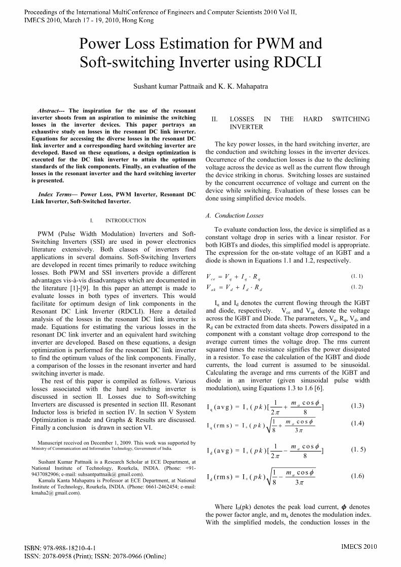
Let us assume an IGBT is carrying a current IQ which is switched off in a zero voltage switching circuit as shown in Figure 1.1; the difference between IQ and the instantaneous device current flows into a resonant capacitor, Cr, connected directly in parallel to the device. This current determines the voltage waveform. An IGBT turn-off waveform for such a case is illustrated in Figure 1.2a. The turn-off current of the IGBT is characterized by a sharp decrease in current, taking only about 50ns for a 50A/600V IGBT. This is a result of the MOSFET part of the IGBT turning off. The bipolar part is still conducting, but the carriers are swept away quickly by tail current. The complete fall time, tf, is about 550ns for the 50A/600V IGBT.
Fig. 1.1 A zero voltage switching circuit for characterizing IGBT turn-off behaviour
Figure 1.2b shows a simplified model of this switching
behavior. Here β denotes a break point of the IGBT current waveform. The value of β ranges from 0.25 to 0.3, obtained from the extensive experimental tests of IGBTs under the zero voltage switching conditions [10]. Considering time ttail as the end of the current flow rather than the fall time, tf, where the current is still 10% of IQ, Under these assumptions, the initial current in the resonant capacitor is (1-β) IQ, and the IGBT current decreases linearly from β IQ to zero taking the time of ttail. The differential equations 1.13 and 1.14 govern the circuit behavior after the IGBT is switched off.
( )r
QcrL r ta il
ta il
Idvi C t td t t
β= + −
(1. 13)
rLr s c r
d iL V v
d t= −
(1.1 4)
F
iLwfo
(
v
MinenEq
E
+
It thim1.spimcathlo
ig. 1.2 (a) Real
(b) Idealize
Solving Equ
Lr(0) = IQ and with the impacound and given
( ) (1
1 c o s
c r t
tω
=
−
Multiplying thntegrating up nergy for thequation 1.16 [
( )o ff Q
S Q
E I Z
V Iβ
=
⎛+ +⎜⎝
is noticed fro
he bus voltampedance, the.16 is directlpecified resonmpedance inapacitance, anhe tail currenosses. With tur
βIQ
10% IQ
listic IGBT turnswi
ed model for ca
uations 1.13 anvcr(0) = 0, thect of the tailn in Equation
)
)
Q
S
I Z
Vt
β
β
−
⎛+⎜
⎝
his voltage to ttail yields
e IGBT carry[10].
2
2 2
(1r Q
Q r
ta il
Z I
I Lt
β β
β
−
⎞ ⎡⎟ ⎢⎣⎠
om Equation
age is mainlerefore, the tuly related to nant frequencydicates a la
nd gives a slowt still persistrn-off energy
(a
(b
n-off waveformitching,
alculation of sof
nd 1.14 with the expression fl current take1.15.
s i nr
Q r
t a i l
t
I Lt
ω
β
+
⎞⎟⎠
with the dean expressio
ying the curre
(
s in1)
1 c2ta i lt
βω ω
ω
⎛ −⎜⎝
−⎡−
⎣
1.15 the rate ly governed
urn-off energy the resonant
y, a smaller vaarger value wer rise of thes and results calculated, sw
ttail
a)
b)
s under zero-vo
ft-switching los
he initial condfor the bus voen into accou
evice current on for the turent IQ as give
)
2
2
co s
ta il
ta il
ta il
ta il
tt
tt
ω
ωω
⎞⎟⎠
⎤⎥⎦
(1
of the increaby the reso
given in Equimpedance.
alue of the resoof the reso
e bus voltage in lower tur
witching losse
oltage
sses
ditions, oltage unt is
(1.1 5)
and rn-off en in
1.1 6)
ase of onant
uation At a
onant onant when rn-off es can
thenswit
Conlossethe these
A. M
In vimainin thautonmodlike samevoltaload lossePmain-cogiven
m aP
B. M
Primon tinduswitpeakturnEquinveand the freqaverhalfthe 1.18
mP
C. E
Sincgaincapaverycapaclamthe r
n be found bching frequen
IV. LOSS
duction and es in the ESRtotal losses ie losses are do
Main Device C
iew of the factn devices withhe main IGBTnomous of th
dulated by thethe hard swit
e supply voltage to the sup
conditions aes of main IGon, are almost tn by Equation
4(ain con− =
Main Device Sw
marily the swithe resonant uctor. As tching losses k load curren
n-off energy, uation 1.16 wierter, the switcdepends mainoutput volt
quency occursrage switchinf the resonantfour main dev
8.
4a in sw− =
ESR Losses
ce the current ned in ESR eacitor can be iy high quality acitor can bemp capacitor iresonant induc
by multiplyinncy.
SES IN THE
switching losRs of the resoin the resonaone individual
Conduction Los
t that there is h the link resoTs (S1-S4) an
he link compoe synchronizetching PWM tage; it is wripply voltage
and for the saGBTs and diothe same as inn 1.9 and are r
( q conP P− +
witching Loss
itching lossescapacitor andexplained in need to be
nt, I0(pk), in aEoff[I0(pk)],
ith IQ replaceching frequencnly on the resotage is zeros, and equals ng frequency t frequency [1vices, Pmain-sw,
0[2
ro ff
f E I
circulates in lements. The ignored sincefactor. Also,
neglected sis very low. Hctor need to be
ng turn-off e
RESONANC
sses in the fionant link aggant inverter. Clly.
ss
a minimal invonance, the cond diodes (D1onents. The red PWM act inverter manoitten off as tratio. Thus,
ame devices, odes in the ren the hard swre-expressed a
)d conP −
s in the main d indirectly o
Section 1.2considered. Ta main devic
can be caed by IQ(pk). cy of the mainonant frequen
o volts, highthe resonant of the main
13]. The switcan be found
0 ( )]p k
the resonant ESR losses
e the resonant the ESR loss
ince the rmsHence, only the considered.
nergy with t
T INVERTER
ive devices agregates to forCalculations f
volvement of tonduction loss-D2) are almoesonant inveralmost exac
oeuvring off tthe same outpunder the samthe conducti
esonant invertwitching inveras Equation 1.
(1.17
devices depenon the resona, only turn-o
Turned- off tce, the resultinalculated usinIn the resonan devices varincy fr, whenevhest switchinfrequency. Tdevices equa
tching losses using Equatio
(1.18
link, losses ain the resonacapacitor has
ses in the clam current in t
he ESR losses
the
R
and rm for
the ses ost rter ctly the put me ion ter, rter .17.
7)
nd ant off the ng ng ant ies ver ng he als in on
8)
are ant s a mp the in
When the resonant inverter operates with a load, the inductor current oscillates tracking the changes of the inverter DC current. The inductor current waveform [14] is given by Equation 1.19
12 0 1212
1( ) [ ]r sI t I Vθ θφ
= − +
(1.1 9)
The ESR value of the resonant inductor is dogged by the inductor quality factor Q. The losses in the resonant inductor, PLr, are then achieved using Equation 1.20.
2r
rL r
ZP IQ
=
(1. 10)
The total losses in the Resonant DC link inverter can now be calculated by adding up the main device losses and the resonant inductor losses, and are represented in Equation 1.21.
rtot m ain con m ain sw LP P P P− −= + +
(1. 21)
V. SYSTEM OPTIMIZATION
The design of the resonant DC link inverter initiates with the selection of the switching devices. Given the device characteristics, the resonant components Lr and Cr can then be preferred to minimize the total losses.
Five-pack 50A/600V IGBT modules (Mitsubishi) are chosen as the main devices of the inverter stage and device of the resonant link.
Limitations to the maximum resonant frequency achievable in the real circuit by several factors include device switching characteristics, thermal constraints, and availability of the passive components [15]. To modulate the inverter for the prototype resonant DC link inverter, a synchronized PWM scheme is used. In this scheme the PWM signals are sampled at the resonant frequency and then synchronized to the zero crossing of the bus voltage. For example, hysteresis bang-bang control is used in PWM inverters for current control within the inverter; however RDCLI uses zero hysteresis bang-bang control; if switches are switched only when the voltage/current is zero and not necessarily when bang-bang controller acts. In order to preserve the well-defined switching pattern of the PWM signals, simulations show that a resonant frequency of about 5 times of the PWM switching frequency is adequate. A resonant frequency of 25-40 kHz is chosen for the design of the link components, considering a maximum PWM switching frequency of 5-8 kHz. If the resonant impedance is known, considering the resonant frequency, the values of the resonant components can be determined.
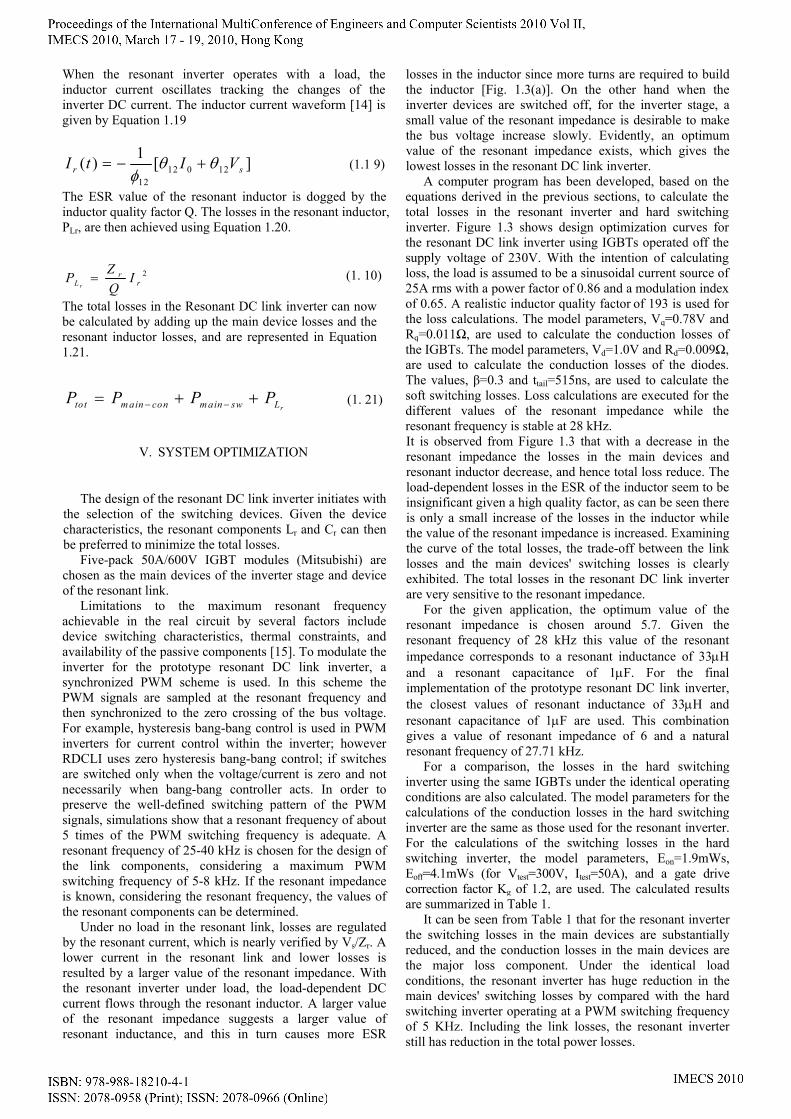
Under no load in the resonant link, losses are regulated by the resonant current, which is nearly verified by Vs/Zr. A lower current in the resonant link and lower losses is resulted by a larger value of the resonant impedance. With the resonant inverter under load, the load-dependent DC current flows through the resonant inductor. A larger value of the resonant impedance suggests a larger value of resonant inductance, and this in turn causes more ESR
losses in the inductor since more turns are required to build the inductor [Fig. 1.3(a)]. On the other hand when the inverter devices are switched off, for the inverter stage, a small value of the resonant impedance is desirable to make the bus voltage increase slowly. Evidently, an optimum value of the resonant impedance exists, which gives the lowest losses in the resonant DC link inverter.
A computer program has been developed, based on the equations derived in the previous sections, to calculate the total losses in the resonant inverter and hard switching inverter. Figure 1.3 shows design optimization curves for the resonant DC link inverter using IGBTs operated off the supply voltage of 230V. With the intention of calculating loss, the load is assumed to be a sinusoidal current source of 25A rms with a power factor of 0.86 and a modulation index of 0.65. A realistic inductor quality factor of 193 is used for the loss calculations. The model parameters, Vq=0.78V and Rq=0.011Ω, are used to calculate the conduction losses of the IGBTs. The model parameters, Vd=1.0V and Rd=0.009Ω, are used to calculate the conduction losses of the diodes. The values, β=0.3 and ttail=515ns, are used to calculate the soft switching losses. Loss calculations are executed for the different values of the resonant impedance while the resonant frequency is stable at 28 kHz. It is observed from Figure 1.3 that with a decrease in the resonant impedance the losses in the main devices and resonant inductor decrease, and hence total loss reduce. The load-dependent losses in the ESR of the inductor seem to be insignificant given a high quality factor, as can be seen there is only a small increase of the losses in the inductor while the value of the resonant impedance is increased. Examining the curve of the total losses, the trade-off between the link losses and the main devices' switching losses is clearly exhibited. The total losses in the resonant DC link inverter are very sensitive to the resonant impedance.
For the given application, the optimum value of the resonant impedance is chosen around 5.7. Given the resonant frequency of 28 kHz this value of the resonant impedance corresponds to a resonant inductance of 33μH and a resonant capacitance of 1μF. For the final implementation of the prototype resonant DC link inverter, the closest values of resonant inductance of 33μH and resonant capacitance of 1μF are used. This combination gives a value of resonant impedance of 6 and a natural resonant frequency of 27.71 kHz.
For a comparison, the losses in the hard switching inverter using the same IGBTs under the identical operating conditions are also calculated. The model parameters for the calculations of the conduction losses in the hard switching inverter are the same as those used for the resonant inverter. For the calculations of the switching losses in the hard switching inverter, the model parameters, Eon=1.9mWs, Eoff=4.1mWs (for Vtest=300V, Itest=50A), and a gate drive correction factor Kg of 1.2, are used. The calculated results are summarized in Table 1.
It can be seen from Table 1 that for the resonant inverter the switching losses in the main devices are substantially reduced, and the conduction losses in the main devices are the major loss component. Under the identical load conditions, the resonant inverter has huge reduction in the main devices' switching losses by compared with the hard switching inverter operating at a PWM switching frequency of 5 KHz. Including the link losses, the resonant inverter still has reduction in the total power losses.

Fig. 1.3 Variation of the losses (a) in Resonant DC Link Inverter due to resonant Impedance, (b) wrt. Frequency,
The lower switching losses allow the resonant inverter to operate at a substantially higher switching frequency, and have a strong potential for realizing higher performance and power density. For the hard switching inverter, on the other hand, switching losses completely dominate the total losses at a high switching frequency of 15 kHz and limit any further increase of the switching frequency. At a low PWM switching frequency of 5 kHz the hard switching inverter is more efficient, where the switching losses are very low and the conduction losses are dominant.
VI. CONCLUSIONS
We presented a detailed analysis of the losses in the resonant DC link inverter. The analysis shows that with the decrease of the resonant impedance the losses in the main devices and resonant link decrease. Using the overall losses as a criterion, the design optimization for the resonant DC link inverter intended for any industrial application yields an optimal value of the resonant impedance as 5.7. This impedance value corresponds to a combination of a resonant inductance of 33μH and a resonant capacitance of 1μF. Loss calculations show that in the resonant inverter the switching losses in the main devices are substantially reduced, and the conduction losses become the major loss component. Under the identical expected load conditions there is significant reduction in the switching losses in the main devices and additionally there is reduction in total losses in comparison to the hard switching counterpart operating at a switching frequency of 15 kHz.
REFERENCES
[1] Divan and G. Skibinski, “Zero switching loss inverters for high power applications.” 1987 IEEE-IAS Annual Meeting Record, pp. 627-634.
[2] He and N. Mohan, “Parallel DC Link Circuit – A Novel Zero Switching loss Topology with Minimum Voltage Stresses.” 1991 IEEE Transactions of Power Electronics, Vol. 6, Number 4, pp.687-694.
[3] He and N. Mohan, W Wold “Zero Voltage Switching PWM Inverter for High Frequency DC-AC Power Conversion” 1990 IEEE-IAS Annual Meeting Record, pp. 1215-1221.
[4] Venkataramanan and D. M. Divan, “Pulse width Modulation With Resonant DC Link Converters” 1990 IEEE-IAS Annual Meeting Record, VOL.II, pp. 984-990.
[5] Divan, “The Resonant DC Link Converter – A New Concept in Static Power Conversion”, 1986 IEEE-IAS Annual Meeting Record, pp 648-665.
[6] Berringer Ken, (1995), "Semiconductor Power Loss in AC Inverter," in Conf. Rec. IEEE-IAS Annual. Meeting, pp. 882-888.
[7] Clemente Steve, (1995), "A Simple Tool for the Selection of IGBTs for Motor Drives and UPSs", in APEC'95 Rec, pp. 755-764.
Frequency
(KHz)
Hard Switching(W) Soft-switching
(W)
Total Losses (W) Conduction Switching Inductor
Hard switching
5 33.34 17.57 50.91 10 33.34 35.14 68.48 15 33.34 52.71 86.05
RDCLI 28 33.34 1.01 21.17 55.52
TABLE 1 Calculated Losses in the HSI and Resonant DC Link Inverter

[8] Azuma, S.; Kimata, M.; Seto, M.; Xinjian Jiang; Haiwei Lu; Dewei Xu; Lipei Huang; “Research on the power loss and junction temperature of power semiconductor devices for inverter,” Vehicle Electronics Conference, 1999. (IVEC '99) Proceedings of the IEEE International, 1999 Page(s):183 – 187.
[9] Ming Zhengfeng; Ni Guangzheng; Zhou Wenyun; Zhong Yanru; “Efficiency Analysis on Soft-Switching Inverters,” Power Electronics and Motion Control Conference, 2004. IPEMC 2004. The 4th International, 2004 Page(s):932 – 935.
[10] Kurnia Alexander, Cherradi Hassan, and Divan Deepakaj M., (1995), “Impact of IGBT Behavior on Design Optimization of Soft Switching Inverter Topologies," IEEE Trans. Ind. Applicat., vol. 31, pp. 280-286, March/April.
[11] Divan Deepakaj M. and Wallace Ian, (1997), “New Developments in Resonant DC Link Inverters," in Conf. Rec. PCC'97-Nagaoka, pp.311-318.
[12] Mertens Axel and Divan Deepakaj M, (1990), " A High Frequency Resonant DC Link Inverter Using IGBTs," in IPEC'90 Rec, pp. 152-160.
[13] Skibinski G. L. and Divan D. M., (1993a), “Design Methodology and Modeling of Low Inductance Planar Bus Structure", in Rec. of Fifth European Conference on Power Electronics and Application, pp.1029-1040.
[14] S. K. Pattnaik and K. K. Mahapatra “A Novel Control Circuit for Aircraft Power Supply Using Soft-Switched Inverter” ICIT, pp.1-6, 2009 IEEE International Conference on Industrial Technology, 2009.
[15] Schulting L., (1992), "A lOO kVA Resonant DC Link Inverter with GTOs - Design Considerations and First Practical Experience," in Conf. Rec. IEEE-IAS Annual. Meeting, pp.729-736.