Power Integrations - Engineering Prototype Report · • Very low cost, low component count...
36
Title Engineering Prototype Report for EP-16 - 2.75 W Charger/Adapter Using LNK501 (LinkSwitch ) Specification 85 VAC to 265 VAC Input, 5.5 V, 500 mA Output Application Low Cost Charger/Adapter Author PI Applications Document Number EPR-16 Date 17-May-04 Revision 1.6 Features • Very low cost, low component count charger/adapter – replaces linear transformer based solutions • Extremely simple circuit configuration designed for high volume, low cost manufacturing – No surface mount components required • Small EE13 transformer allows compact size • Approximate constant voltage, constant current (CV/CC) primary sensed output characteristic – No optocoupler or sense resistors required • Efficiency greater than 71% • No-load power consumption <300 mW at 265 VAC • No Y1 safety capacitor required – Only transformer bridges primary-to-secondary safety barrier – Ultra low leakage design (<5 µA) The products and applications illustrated herein (including circuits external to the products and transformer construction) may be covered by one or more U.S. and foreign patents or potentially by pending U.S. and foreign patent applications assigned to Power Integrations. A complete list of Power Integrations’ patents may be found at www.powerint.com . Power Integrations 5245 Hellyer Avenue, San Jose, CA 95138 USA. Applications Hotline: Tel: +1 408 414 9660 Fax: +1 408 414 9760 www.powerint.com
-
Upload
trinhthuan -
Category
Documents
-
view
214 -
download
0
Transcript of Power Integrations - Engineering Prototype Report · • Very low cost, low component count...

Title Engineering Prototype Report for EP-16 - 2.75 W Charger/Adapter Using LNK501 (LinkSwitch)
Specification 85 VAC to 265 VAC Input, 5.5 V, 500 mA Output
Application Low Cost Charger/Adapter
Author PI Applications
Document Number EPR-16
Date 17-May-04
Revision 1.6 Features • Very low cost, low component count charger/adapter – replaces
linear transformer based solutions • Extremely simple circuit configuration designed for high volume,
low cost manufacturing – No surface mount components required
• Small EE13 transformer allows compact size • Approximate constant voltage, constant current (CV/CC) primary
sensed output characteristic – No optocoupler or sense resistors required
• Efficiency greater than 71% • No-load power consumption <300 mW at 265 VAC • No Y1 safety capacitor required
– Only transformer bridges primary-to-secondary safety barrier – Ultra low leakage design (<5 µA)
The products and applications illustrated herein (including circuits external to the products and transformer construction) may be covered by one or more U.S. and foreign patents or potentially by pending U.S. and foreign patent applications assigned to Power Integrations. A complete list of Power Integrations’ patents may be found at www.powerint.com.
Power Integrations
5245 Hellyer Avenue, San Jose, CA 95138 USA. Applications Hotline: Tel: +1 408 414 9660 Fax: +1 408 414 9760
www.powerint.com

EPR-16 - LinkSwitch 2.75 W Charger/Adapter 17-May-04
Table Of Contents 1 Introduction.................................................................................................................4 2 Power Supply Specification ........................................................................................5 3 Schematic...................................................................................................................7 4 Circuit Description ......................................................................................................8
4.1 Input Stage ..........................................................................................................8 4.2 LinkSwitch Operation ..........................................................................................9 4.3 Transformer.......................................................................................................10 4.4 Clamp and Feedback Components ...................................................................10 4.5 Output Stage .....................................................................................................11
5 PCB Layout ..............................................................................................................12 6 Bill Of Materials ........................................................................................................13 7 Transformer ..............................................................................................................14
7.1 Transformer Winding.........................................................................................14 7.2 Electrical Specifications.....................................................................................14 7.3 Materials............................................................................................................15 7.4 Transformer Build Diagram ...............................................................................15 7.5 Transformer Construction..................................................................................16
8 Performance Data ....................................................................................................17 8.1 Line and Load Regulation..................................................................................17 8.2 Efficiency ...........................................................................................................18 8.3 No-Load Input Power ........................................................................................18
9 Waveforms ...............................................................................................................19 9.1 Drain Voltage and Current Waveforms..............................................................19
9.1.1 90 VAC, Normal Operation.........................................................................19 9.1.2 265 VAC, Normal Operation.......................................................................19
9.2 Output Voltage Start-up Profile..........................................................................20 9.3 Load Transient Response (0.25 A to 0.5 A Load Step) .....................................20 9.4 Output Ripple Measurements............................................................................21
9.4.1 Ripple Measurement Technique ................................................................21 9.4.2 Output Voltage Ripple ................................................................................22
9.5 Thermal Measurements ....................................................................................23 9.6 Conducted EMI..................................................................................................24
9.6.1 Optional Components With Artificial Hand .................................................25 9.6.2 Optional Components Without Artificial Hand ............................................25 9.6.3 Optional Components Removed With Artificial Hand .................................26
10 Appendix A – EP-16 Enclosure Opening Procedures ..............................................27 10.1 Method 1 - Non-destructive ...............................................................................27 10.2 Method 2 - Destructive ......................................................................................27
11 Appendix B – LNK520P in the High-Side Configuration ..........................................28 11.1 Introduction........................................................................................................28 11.2 Comparison of LNK501 and LNK520 ................................................................28 11.3 Circuit Changes.................................................................................................29 11.4 Performance Data .............................................................................................30
11.4.1 Line and Load Regulation ..........................................................................30 11.4.2 Efficiency....................................................................................................31
Page 2 of 36 Power Integrations
Tel: +1 408 414 9660 Fax: +1 408 414 9760 www.powerint.com

17-May-04 EPR-16 – LinkSwitch 2.75 W Charger/Adapter
11.4.3 No-Load Input Power..................................................................................32 11.5 EMI Performance...............................................................................................33
12 Revision History........................................................................................................34 Important Note: Although the EP-16 is designed to satisfy safety isolation requirements, this engineering prototype has not been agency approved. Therefore, all testing should be performed using an isolation transformer to provide the AC input to the prototype board.
Page 3 of 36 Power Integrations
Tel: +1 408 414 9660 Fax: +1 408 414 9760www.powerint.com
EPR-16 - LinkSwitch 2.75 W Charger/Adapter 17-May-04
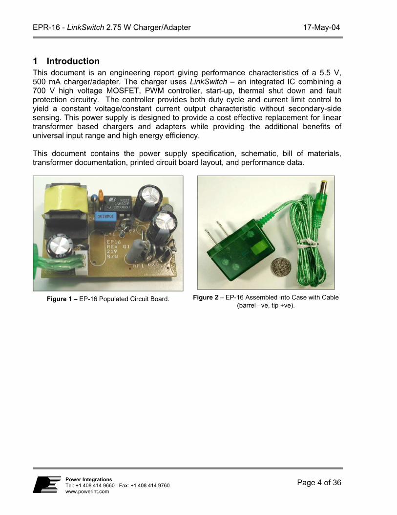
1 Introduction This document is an engineering report giving performance characteristics of a 5.5 V, 500 mA charger/adapter. The charger uses LinkSwitch – an integrated IC combining a 700 V high voltage MOSFET, PWM controller, start-up, thermal shut down and fault protection circuitry. The controller provides both duty cycle and current limit control to yield a constant voltage/constant current output characteristic without secondary-side sensing. This power supply is designed to provide a cost effective replacement for linear transformer based chargers and adapters while providing the additional benefits of universal input range and high energy efficiency. This document contains the power supply specification, schematic, bill of materials, transformer documentation, printed circuit board layout, and performance data.
Figure 1 – EP-16 Populated Circuit Board.
Figure 2 – EP-16 Assembled into Case with Cable (barrel −ve, tip +ve).
Page 4 of 36 Power Integrations
Tel: +1 408 414 9660 Fax: +1 408 414 9760 www.powerint.com

17-May-04 EPR-16 – LinkSwitch 2.75 W Charger/Adapter
2 Power Supply Specification
Description Symbol Min Typ Max Units Comment Input Voltage VIN 85 265 VAC 2 Wire – no Protective Ground Frequency fLINE 47 50/60 64 Hz No-load Input Power (265 VAC) 0.3 W
Output Output Voltage VOUT 5.0 5.5 6.0 V At peak output power point Output Ripple Voltage (res. load) VRIPPLE R 300 mV Resistive load, peak power Output Ripple Voltage (bat. load) VRIPPLE B 150 mV Battery load, peak power Output Current 1 IOUT 400 500 600 mA Total Output Power Continuous Output Power POUT 2 2.75 3.6 W
Efficiency η 71 % Measured at output peak power point, 25 oC
Environmental
1.2/50 Surge 2 kV 1.2/50 µs surge, IEC 1000-4-5,
12 Ω series impedance, differential and common mode
100 kHz Ring Wave Surge 2 kV 100 kHz ring wave, 500 A short circuit current, differential and
common mode
Ambient Temperature TAMB 0 40 oC Free convection, sea level
Conducted EMI Meets CISPR22B / EN55022B & FCC B with artificial hand connected to output return
Safety Designed to meet IEC950, UL1950 Class II
Output VI Characteristic Specification
0
1
2
3
4
5
6
7
8
9
10
0 100 200 300 400 500 600 700IOUT (mA)
V OU
T (D
C)
Figure 3 – EP-16 Output Characteristic Envelope. (Shading represents no-go areas.)
Page 5 of 36 Power Integrations
Tel: +1 408 414 9660 Fax: +1 408 414 9760www.powerint.com
EPR-16 - LinkSwitch 2.75 W Charger/Adapter 17-May-04
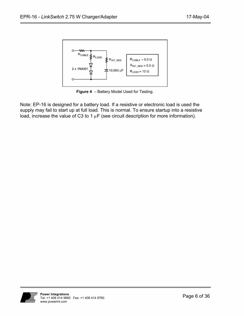
Figure 4 – Battery Model Used for Testing.
Note: EP-16 is designed for a battery load. If a resistive or electronic load is used the supply may fail to start up at full load. This is normal. To ensure startup into a resistive load, increase the value of C3 to 1 µF (see circuit description for more information).
Page 6 of 36 Power Integrations
Tel: +1 408 414 9660 Fax: +1 408 414 9760 www.powerint.com
17-May-04 EPR-16 – LinkSwitch 2.75 W Charger/Adapter
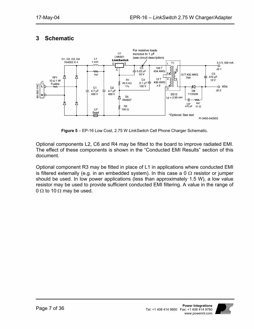
3 Schematic
Figure 5 – EP-16 Low Cost, 2.75 W LinkSwitch Cell Phone Charger Schematic.
Optional components L2, C6 and R4 may be fitted to the board to improve radiated EMI. The effect of these components is shown in the “Conducted EMI Results” section of this document. Optional component R3 may be fitted in place of L1 in applications where conducted EMI is filtered externally (e.g. in an embedded system). In this case a 0 Ω resistor or jumper should be used. In low power applications (less than approximately 1.5 W), a low value resistor may be used to provide sufficient conducted EMI filtering. A value in the range of 0 Ω to 10 Ω may be used.
Page 7 of 36 Power Integrations
Tel: +1 408 414 9660 Fax: +1 408 414 9760www.powerint.com

EPR-16 - LinkSwitch 2.75 W Charger/Adapter 17-May-04
4 Circuit Description The schematic shown in Figure 5 provides a CV/CC (constant voltage/constant current) type output characteristic from a universal input voltage range of 85 VAC to 265 VAC. The nominal peak power point at the transition from CC to CV is 5.5 V at 500 mA. The precise output envelope specification is shown in Figure 3.
4.1 Input Stage The incoming AC is rectified and filtered by D1-4, C1 and C2. Resistor RF1 is a flameproof fusible type to protect against fault conditions and is a requirement to meet safety agency fault testing. This component should be a wire wound type to withstand input current surges while the input capacitors charge on application of power or during withstand line-transient testing. Metal film type resistors are not recommended, they do not have the transient dissipation capabilities required and may fail prematurely in the field. Lower values increase the resistor dissipation (V²/R power term) during transients, increasing resistor stress, while higher values increase steady state dissipation (I²R power term) and reduce efficiency. If a suitable flame proof resistor cannot be found (during failure flame proof resistors do not emit flames, smoke or incandescent material that may damage transformer insulation), then a standard fusible type may be used as long as a protective heat shrink sleeve is placed over the resistor. Please consult with a safety engineer or local safety agency. The value of C1 and C2 were selected to provide the smallest standard values to meet 3 µF/W, in this case two 4.7 µF, 400 V capacitors. Smaller values are possible (either 2.2 µF or 3.3 µF) however, the lower DC rail voltage will increase LinkSwitch dissipation, lowering efficiency and increasing line frequency output ripple. Differential mode EMI (<500 kHz) also typically increases. The input capacitance is split between C1 and C2 to allow an input π filter to be formed by L1. This filters noise associated with the supply to meet EN55022B / CISPR 22 B and FCC B conducted EMC limits, even when no Y safety capacitor is used. Ferrite bead L2 is optional, fitted to improve radiated EMI.
Page 8 of 36 Power Integrations
Tel: +1 408 414 9660 Fax: +1 408 414 9760 www.powerint.com

17-May-04 EPR-16 – LinkSwitch 2.75 W Charger/Adapter
4.2 LinkSwitch Operation When power is applied to the supply, high voltage DC appears at the DRAIN pin of LinkSwitch (U1). The CONTROL pin capacitor C3 is then charged through a switched high voltage current source connected internally between the DRAIN and CONTROL pins. When the CONTROL pin voltage reaches approximately 5.7 V relative to the SOURCE pin, the internal current source is turned off. The internal control circuitry is activated and the high voltage internal MOSFET starts to switch, using the energy in C3 to power the IC. As the current ramps in the primary of flyback transformer T1, energy is stored. This energy is delivered to the output when the MOSFET turns off each cycle. The secondary of the transformer is rectified and filtered by D6 and C5 to provide the DC output to the load. Control of the output characteristic is entirely sensed from the primary-side by monitoring the primary-side VOR (voltage output reflected). While the output diode is conducting, the voltage across the transformer primary is equal to the output voltage plus diode drop multiplied by the turns ratio of the transformer. Since the LinkSwitch is connected on the high side of the transformer, the VOR can be sensed directly. Diode D5 and capacitor C4 form the primary clamp network. The voltage held across C4 is essentially the VOR with an error due to the parasitic leakage inductance. The LinkSwitch has three operating modes determined by the current flowing into the CONTROL pin. During start-up, as the output voltage, and therefore the reflected voltage and voltage across C4 increases, the feedback current increases from 0 to approximately 2 mA through R1 into the CONTROL pin. The internal current limit is increased during this period until reaching 100%, providing an approximately constant output current. Once the output voltage reaches the regulated CV value, the output voltage is regulated through control of the duty cycle. As the current into the CONTROL pin exceeds approximately 2 mA, the duty cycle begins to reduce, reaching 30% at a CONTROL pin current of 2.3 mA. If the duty cycle reaches a 3% threshold, the switching frequency is reduced, which reduces energy consumption under light or no load conditions. As the output load increases beyond the peak power point (defined by ½·L·I²·f) and the output voltage and VOR falls, the reduced CONTROL pin current will lower the internal current providing an approximately constant current output characteristic. If the output load is further increased and the output voltage falls further to below a CONTROL pin current of 1 mA, the CONTROL pin capacitor C3 will discharge and the supply will enter auto-restart.
Page 9 of 36 Power Integrations
Tel: +1 408 414 9660 Fax: +1 408 414 9760www.powerint.com
EPR-16 - LinkSwitch 2.75 W Charger/Adapter 17-May-04
4.3 Transformer The transformer is designed to always be discontinuous; all the energy is transferred to the load during the MOSFET off time. The energy stored in the transformer during discontinuous mode operation is ½·L·I²·f, where L is the primary inductance, I² is the peak primary current squared and f is the switching frequency. Since the value of LinkSwitch current limit and frequency directly determines the peak power or CV/CC transition point in the output characteristic, the parameter of current squared times frequency is defined in the datasheet. This parameter, together with the output power, is used to specify the transformer primary inductance. With a primary inductance tolerance of ±10%, the EP-16 is designed to provide the output current characteristic shown in Figure 3∗. As LinkSwitch is powered by the energy stored in the leakage inductance of the transformer, only a low cost two winding transformer is required. Leakage inductance should be kept low, ideally at less than 2% of the primary inductance. High leakage inductance will cause the CC characteristic to walk out as the output voltage decreases and increases the no-load consumption of the supply. With a figure of 50 µH for leakage, this design is able to meet a voltage tolerance of ±10% at the peak power point, including the effects of output cable drop. For tighter voltage tolerance across the whole load range, a secondary optocoupler can be added. For most battery charging applications, only the voltage at the peak power point is critical, thus ensuring sufficient voltage for charging.
4.4 Clamp and Feedback Components Diode D5 should either be a fast (trr <250 ns) or ultra-fast type to prevent the voltage across LinkSwitch from reversing and ringing below ground. A fast diode is preferred, being lower cost. Leakage inductance is filtered by R2, the optimum value providing the straightest CC characteristic. Capacitor C4 is typically fixed at 0.1 µF and should be rated above the VOR and be stable with both temperature and applied voltage. Low-cost, metalized plastic film capacitors are ideal; high value, low-cost ceramic capacitors are not recommended. Dielectrics used for these capacitors such as Z5U and Y5U are not stable and can cause output instability as their value changes with voltage and temperature. Stable dielectrics such as COG/NPO are acceptable but are costly when compared to a metalized plastic film capacitor.
Page 10 of 36 Power Integrations
Tel: +1 408 414 9660 Fax: +1 408 414 9760 www.powerint.com
∗ This includes LinkSwitch tolerance and line variation.

17-May-04 EPR-16 – LinkSwitch 2.75 W Charger/Adapter
R1 was selected to program the peak power point to be 500 mA when a transformer with a nominal LP value was used. Initial values are selected using the expression (from Power Integrations Application note, AN-35):
R1 ≅ (VFB - VC (IDCT)) / IDCT
≅ (54.1 – 5.75) / 2.3 mA ≅ 21 kΩ
The closest standard 1% series value of 20.5 kΩ was selected. See AN-35 for a more detailed explanation of clamp and feedback component selection. C3 sets the auto-restart period and also the time the output has to reach regulation before entering auto-restart from start-up. If a battery load is used then a value of 0.22 µF is typical. However, if the supply is required to start into a resistive load then this should be increased to 1 µF to ensure enough time during start-up to bring the output into regulation. The type of capacitor is not critical; either a small ceramic or electrolytic may be used with a voltage rating of 10 V or more.
4.5 Output Stage Diode D6 should be rated for 80% of applied reverse voltage and thermally for average current multiplied by forward voltage at maximum ambient. Here a 1 A, 60 V Schottky diode was used to reduce the losses and improve efficiency, although fast or ultra-fast PN diodes are acceptable. A snubber formed by C6 and R4 may be fitted across D6 to improve radiated EMI performance. Capacitor C5 should be rated for output voltage and ripple current. Depending on the application, the designer may choose not to derate for ripple current. If the application is battery charging of equipment such as PDAs or cell phones, the duty cycle of operation at high ripple current is likely to be low, perhaps only 1 hour per day. In this case the capacitor temperature can be allowed to rise significantly during charging without concern for the overall capacitor lifetime.
Page 11 of 36 Power Integrations
Tel: +1 408 414 9660 Fax: +1 408 414 9760www.powerint.com
EPR-16 - LinkSwitch 2.75 W Charger/Adapter 17-May-04
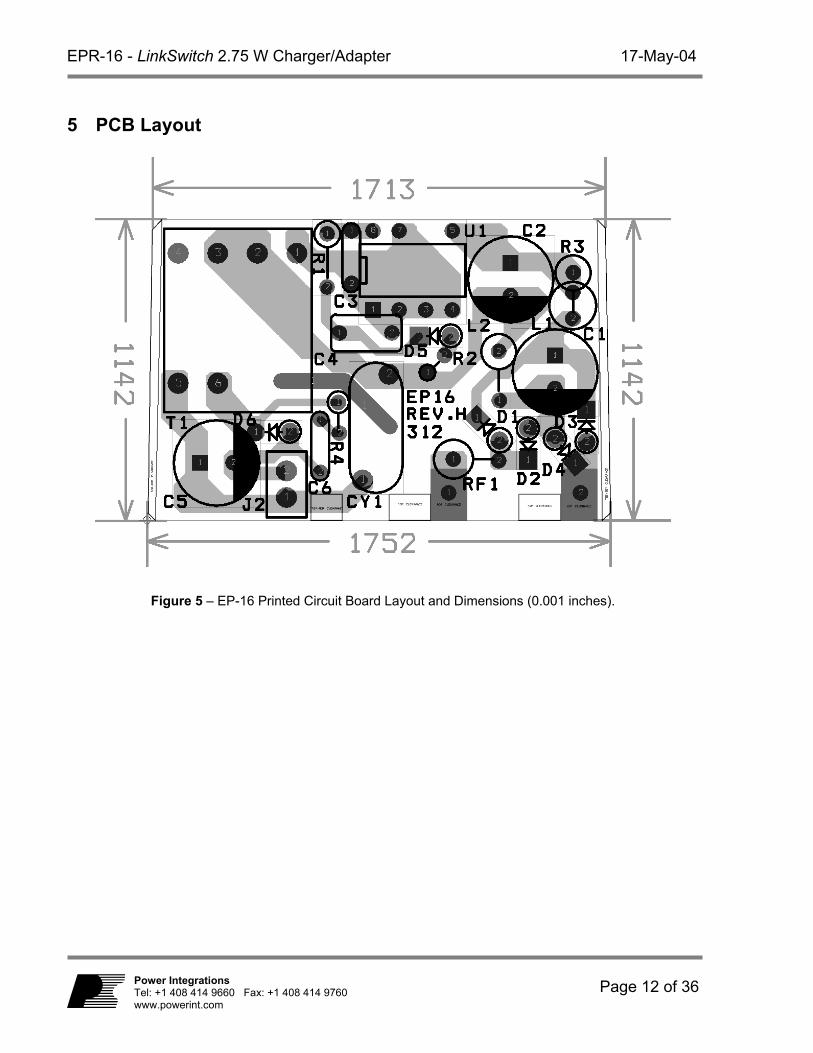
5 PCB Layout
Figure 5 – EP-16 Printed Circuit Board Layout and Dimensions (0.001 inches).
Page 12 of 36 Power Integrations
Tel: +1 408 414 9660 Fax: +1 408 414 9760 www.powerint.com
17-May-04 EPR-16 – LinkSwitch 2.75 W Charger/Adapter
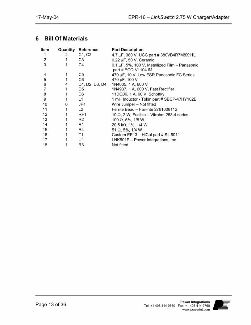
6 Bill Of Materials
Item Quantity Reference Part Description 1 2 C1, C2 4.7 µF, 380 V, UCC part # 380VB4R7M8X11L 2 1 C3 0.22 µF, 50 V, Ceramic 3 1 C4 0.1 µF, 5%, 100 V, Metallized Film – Panasonic
part # ECQ-V1104JM 4 1 C5 470 µF, 10 V, Low ESR Panasonic FC Series 5 1 C6 470 pF, 100 V 6 4 D1, D2, D3, D4 1N4005, 1 A, 600 V 7 1 D5 1N4937, 1 A, 600 V, Fast Rectifier 8 1 D6 11DQ06, 1 A, 60 V, Schottky 9 1 L1 1 mH Inductor - Tokin part # SBCP-47HY102B 10 0 JP1 Wire Jumper – Not fitted 11 1 L2 Ferrite Bead – Fair-rite 2761008112 12 1 RF1 10 Ω, 2 W, Fusible – Vitrohm 253-4 series 13 1 R2 100 Ω, 5%, 1/8 W 14 1 R1 20.5 kΩ, 1%, 1/4 W 15 1 R4 51 Ω, 5%, 1/4 W 16 1 T1 Custom EE13 – HiCal part # SIL6011 17 1 U1 LNK501P – Power Integrations, Inc 18 1 R3 Not fitted
Page 13 of 36 Power Integrations
Tel: +1 408 414 9660 Fax: +1 408 414 9760www.powerint.com
EPR-16 - LinkSwitch 2.75 W Charger/Adapter 17-May-04
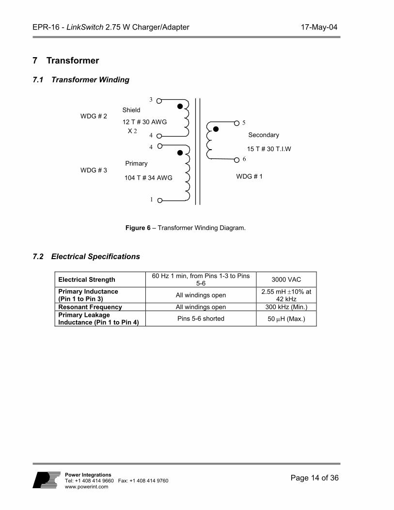
7 Transformer
7.1 Transformer Winding
4
1
4
3
5
6
Shield
Primary
Secondary
12 T # 30 AWG
104 T # 34 AWG
15 T # 30 T.I.W
WDG # 3 WDG # 1
WDG # 2
X 2
Figure 6 – Transformer Winding Diagram.
7.2 Electrical Specifications
Electrical Strength 60 Hz 1 min, from Pins 1-3 to Pins 5-6 3000 VAC
Primary Inductance (Pin 1 to Pin 3) All windings open 2.55 mH ±10% at
42 kHz Resonant Frequency All windings open 300 kHz (Min.) Primary Leakage Inductance (Pin 1 to Pin 4) Pins 5-6 shorted 50 µH (Max.)
Page 14 of 36 Power Integrations
Tel: +1 408 414 9660 Fax: +1 408 414 9760 www.powerint.com

17-May-04 EPR-16 – LinkSwitch 2.75 W Charger/Adapter
7.3 Materials
Item Description [1] Core: EE13, PC40EE13, TDK – ALG 190 nH/t2 [2] Bobbin: Horizontal 8pin – pins 7 and 8 removed [3] Magnet Wire: #34 AWG [4] Magnet Wire: #30 AWG [5] Triple Insulated Wire: #30 AWG. [6] Tape: 3M 1298 Polyester Film (white) 320mils wide by 2.2 mils thick [7] Tape: 3M 1298 Polyester Film (white) 290mils wide by 2.2 mils thick [8] Glue AV118 [9] Copper tape 6mm +/- 0.15 mm wide by 0.076 mm thick
Design Notes: Power Integrations Device LNK501 Frequency of Operation 42 kHz Mode Discontinuous Peak Current 0.263 A Reflected Voltage (Secondary to Primary) 48 V Maximum DC Input Voltage 370 V Minimum DC Input Votlage 90 V
7.4 Transformer Build Diagram
Figure 7 – EP-16 Transformer Build Diagram.
Page 15 of 36 Power Integrations
Tel: +1 408 414 9660 Fax: +1 408 414 9760www.powerint.com

EPR-16 - LinkSwitch 2.75 W Charger/Adapter 17-May-04
7.5 Transformer Construction
Secondary Winding Start at Pin 4 temporarily. Wind 15 turns of item [5] from right to left with tight tension. Wind uniformly, in a single layer across entire width of bobbin. Finish on Pin 6.
Basic Insulation 1 Layer of tape [6] for insulation. Secondary Winding Change the start pin connection of secondary winding from Pin 4 to Pin 5.
Basic Insulation 1 Layer of tape [6] for insulation.
Cancellation Winding
Start at Pin 3. Wind 12 turns of bifilar item [4] from right to left with tight tension. Wind uniformly, in a single layer, across entire width of bobbin. Finish on Pin 4.
Basic Insulation 1 Layer of tape [6] for insulation.
Primary Winding 2 2/3 Layer
Start at Pin 4. Wind 104 turns of item [3] from right to left in 2 and 2/3 layers across entire width of bobbin. Wind all layers with tight tension. Finish on Pin 1.
Outer Insulation 10 Layer of tape [7] for insulation. Core Assembly Assemble and secure core halves using item [8]
Flux / Belly band Place item [9] around outside of windings and core halves with tight tension. Make electrical connection to band from pin 3 using item [4].
Basic Insulation 2 layers of tape [6] for insulation. Crop Unused Pins Remove pins 7 and 8
Note: The transformer is an integral part of the EMI performance of this design. Changes to the transformer may have significant impact on both conducted and radiated EMI.
Page 16 of 36 Power Integrations
Tel: +1 408 414 9660 Fax: +1 408 414 9760 www.powerint.com
17-May-04 EPR-16 – LinkSwitch 2.75 W Charger/Adapter
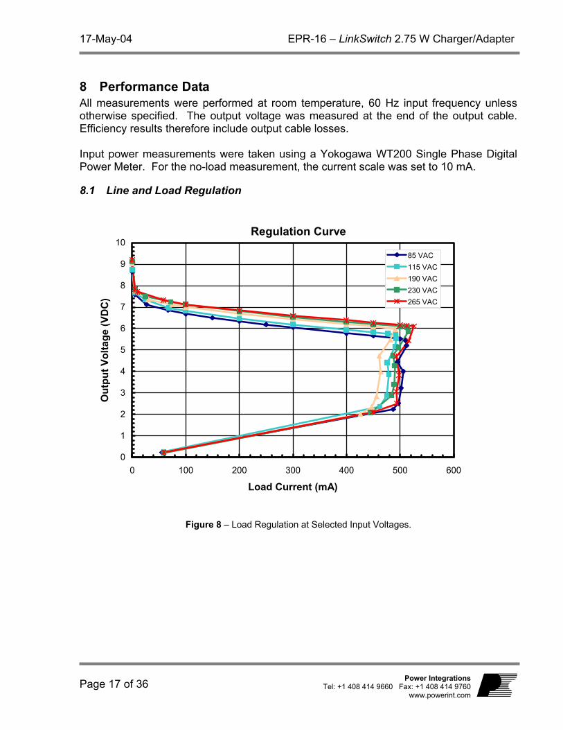
8 Performance Data All measurements were performed at room temperature, 60 Hz input frequency unless otherwise specified. The output voltage was measured at the end of the output cable. Efficiency results therefore include output cable losses. Input power measurements were taken using a Yokogawa WT200 Single Phase Digital Power Meter. For the no-load measurement, the current scale was set to 10 mA.
8.1 Line and Load Regulation
Regulation Curve
0
1
2
3
4
5
6
7
8
9
10
0 100 200 300 400 500 600
Load Current (mA)
Out
put V
olta
ge (V
DC
)
85 VAC115 VAC190 VAC230 VAC265 VAC
Figure 8 – Load Regulation at Selected Input Voltages.
Page 17 of 36 Power Integrations
Tel: +1 408 414 9660 Fax: +1 408 414 9760www.powerint.com

EPR-16 - LinkSwitch 2.75 W Charger/Adapter 17-May-04
8.2 Efficiency
Efficiency vs. Output Current
0
10
20
30
40
50
60
70
80
0 100 200 300 400 500 600
Load Current (mA)
Effic
ienc
y (%
)
85 VAC115 VAC190 VAC230 VAC265 VAC
Figure 9 – Efficiency vs. Output Current at Selected Input Voltages.
8.3 No-Load Input Power
No-Load Consumption
0
0.05
0.1
0.15
0.2
0.25
0.3
0.35
80 100 120 140 160 180 200 220 240 260 280
AC Input Voltage (VAC)
Inpu
t Pow
er (m
W)
Figure 10 – Zero Load Input Power vs. Input Line Voltage.
Page 18 of 36 Power Integrations
Tel: +1 408 414 9660 Fax: +1 408 414 9760 www.powerint.com
17-May-04 EPR-16 – LinkSwitch 2.75 W Charger/Adapter
9 Waveforms
9.1 Drain Voltage and Current Waveforms
9.1.1 90 VAC, Normal Operation
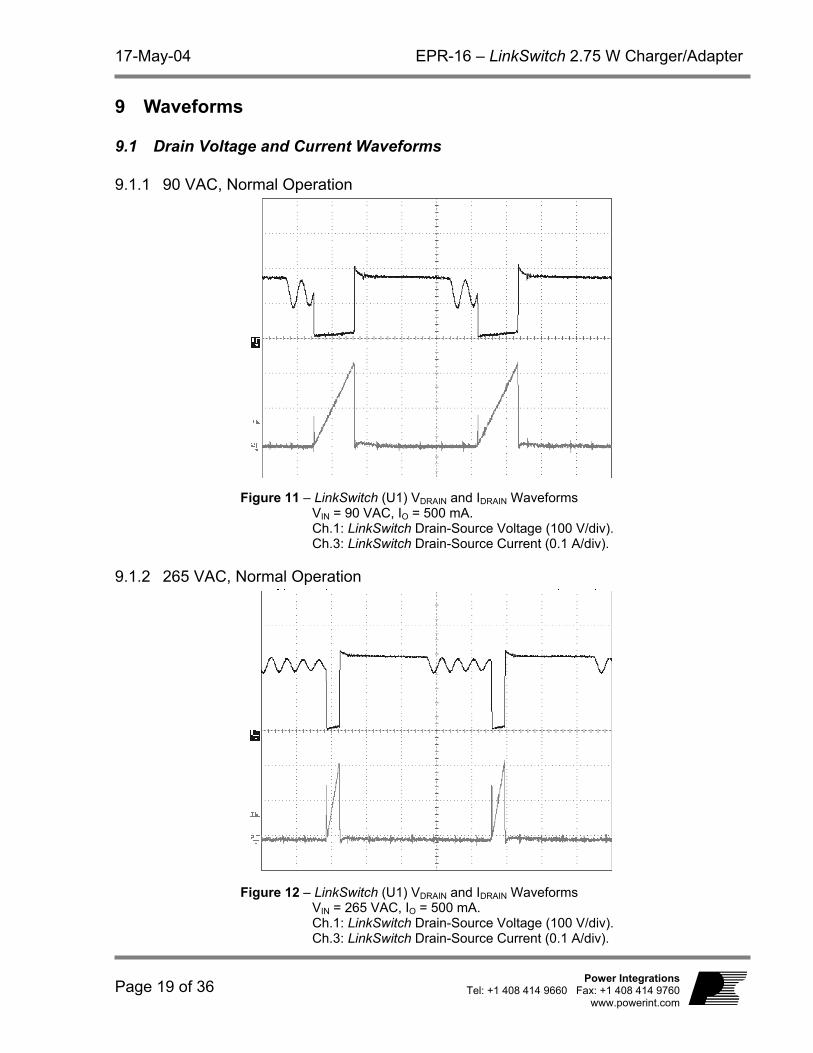
Figure 11 – LinkSwitch (U1) VDRAIN and IDRAIN Waveforms
VIN = 90 VAC, IO = 500 mA. Ch.1: LinkSwitch Drain-Source Voltage (100 V/div). Ch.3: LinkSwitch Drain-Source Current (0.1 A/div).
9.1.2 265 VAC, Normal Operation
Figure 12 – LinkSwitch (U1) VDRAIN and IDRAIN Waveforms
VIN = 265 VAC, IO = 500 mA. Ch.1: LinkSwitch Drain-Source Voltage (100 V/div). Ch.3: LinkSwitch Drain-Source Current (0.1 A/div).
Page 19 of 36 Power Integrations
Tel: +1 408 414 9660 Fax: +1 408 414 9760www.powerint.com

EPR-16 - LinkSwitch 2.75 W Charger/Adapter 17-May-04
9.2 Output Voltage Start-up Profile
Figure 13 – Output Voltage at Start-up, Battery
Model, VIN = 90 VAC, POUT_MAX.
Figure 14 – Output Voltage at Start-up, Battery
Model, VIN = 265 VAC, POUT_MAX.
9.3 Load Transient Response (0.25 A to 0.5 A Load Step)
Figure 15 – Dynamic Load Transient
0.25 A to 0.5 A step at VIN = 90 VAC. Ch.3: Output Voltage (500 mV/div).
Figure 16 – Dynamic Load Transient
0.25 A to 0.5 A step at VIN = 265 VAC. Ch.3: Output Voltage (500 mV/div).
Page 20 of 36 Power Integrations
Tel: +1 408 414 9660 Fax: +1 408 414 9760 www.powerint.com

17-May-04 EPR-16 – LinkSwitch 2.75 W Charger/Adapter
9.4 Output Ripple Measurements
9.4.1 Ripple Measurement Technique For DC output ripple measurements, a modified oscilloscope test probe must be utilized in order to reduce spurious signals due to pickup. Details of the probe modification are provided in Figure 17 and Figure 18. The 5125BA probe adapter is affixed with two capacitors tied in parallel across the probe tip. The capacitors include one (1) 0.1 µF/50 V ceramic type and one (1) 1.0 µF/50 V aluminum electrolytic.
Probe Ground
Probe Tip
Figure 17 – Oscilloscope Probe Prepared for Ripple Measurement. (End cap and ground lead removed).
Figure 18 – Oscilloscope Probe with Probe Master 5125BA BNC Adapter.
(Modified with wires for probe ground for ripple measurement and two parallel decoupling capacitors added).
Page 21 of 36 Power Integrations
Tel: +1 408 414 9660 Fax: +1 408 414 9760www.powerint.com

EPR-16 - LinkSwitch 2.75 W Charger/Adapter 17-May-04
9.4.2 Output Voltage Ripple
Measurements are shown for both resistive and battery model loads (Figure 4).
Figure 19 – Output Voltage Ripple (Resistive)
at VIN = 115 VAC, VO = 5.2 V, IO = 500 mA (Scale: 100 mV/div).
Figure 20 – Output Voltage Ripple (Resistive)
at VIN = 230 VAC, VO = 5.3 V, IO = 515 mA (Scale: 100 mV/div).
Figure 21 – Output Voltage Ripple (Battery)
at VIN = 115 VAC, Vo = 5.2 V, Io = 500 mA (Scale: 100 mV, 5 ms,100 µs / div).
Figure 22 – Output Voltage Ripple (Battery)
at VIN = 230 VAC, Vo = 5.3 V, Io = 500 mA (Scale: 100 mV, 5 ms,100 µs / div).
Page 22 of 36 Power Integrations
Tel: +1 408 414 9660 Fax: +1 408 414 9760 www.powerint.com
17-May-04 EPR-16 – LinkSwitch 2.75 W Charger/Adapter
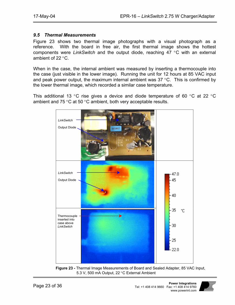
9.5 Thermal Measurements Figure 23 shows two thermal image photographs with a visual photograph as a reference. With the board in free air, the first thermal image shows the hottest components were LinkSwitch and the output diode, reaching 47 °C with an external ambient of 22 °C. When in the case, the internal ambient was measured by inserting a thermocouple into the case (just visible in the lower image). Running the unit for 12 hours at 85 VAC input and peak power output, the maximum internal ambient was 37 °C. This is confirmed by the lower thermal image, which recorded a similar case temperature. This additional 13 °C rise gives a device and diode temperature of 60 °C at 22 °C ambient and 75 °C at 50 °C ambient, both very acceptable results.
LinkSwitch Output Diode
LinkSwitch Output Diode
Thermocouple inserted into case above LinkSwitch
Figure 23 - Thermal Image Measurements of Board and Sealed Adapter, 85 VAC Input, 5.3 V, 500 mA Output, 22 °C External Ambient
Page 23 of 36 Power Integrations
Tel: +1 408 414 9660 Fax: +1 408 414 9760www.powerint.com

EPR-16 - LinkSwitch 2.75 W Charger/Adapter 17-May-04
9.6 Conducted EMI All measurements were taken at the peak output power point with a line voltage of 230 VAC. This line voltage represents the worst case; results are lower at 115 VAC. Limts shown are for EN55022B / CISPR22B Final measurements were taken in all cases, representing the worst case of both phase and indicated as either “X” on quasi peak results or “+” on average results. Results with and without the optional components L2, R4 and C6 are shown to illustrate the improvement in radiated EMI (50 MHz to 60 MHz region). In all cases, a 10 dB or greater margin was obtained.
Page 24 of 36 Power Integrations
Tel: +1 408 414 9660 Fax: +1 408 414 9760 www.powerint.com

17-May-04 EPR-16 – LinkSwitch 2.75 W Charger/Adapter
9.6.1 Optional Components With Artificial Hand
Figure 24 – EN55022 B / CISPR22 B, VIN = 230 VAC, 60 Hz Line, Peak
Power Point, Output Return Connected to Artificial Hand Input on LISN.
9.6.2 Optional Components Without Artificial Hand
Figure 25 – EN55022 B / CISPR22 B, VIN = 230 VAC, 60 Hz Line, Peak
Power Point, Output Floating.
Page 25 of 36 Power Integrations
Tel: +1 408 414 9660 Fax: +1 408 414 9760www.powerint.com

EPR-16 - LinkSwitch 2.75 W Charger/Adapter 17-May-04
9.6.3 Optional Components Removed With Artificial Hand
Figure 26 - EN55022 B / CISPR22 B, VIN = 230 VAC, 60 Hz Line, Peak
Power Point, Output Return Connected to Artificial Hand Input on LISN.
Figure 27 - EN55022 B / CISPR22 B, VIN = 230 VAC, 60 Hz Line, Peak
Power Point, Output Return Floating.
Page 26 of 36 Power Integrations
Tel: +1 408 414 9660 Fax: +1 408 414 9760 www.powerint.com

17-May-04 EPR-16 – LinkSwitch 2.75 W Charger/Adapter
10 Appendix A – EP-16 Enclosure Opening Procedures
10.1 Method 1 - Non-destructive
Step 1: Insert thin bladed
screwdrivers into slots in the AC connect portion of case. Make certain screwdriver is on top of plastic tab.
Step 2: Insert thin bladed screwdriver between two halves of the case and twist. Case will pop apart. Repeat on other side and pull to separate.
Figure 28 – Non-destructive Opening of EP-16 Case.
10.2 Method 2 - Destructive
Step 1: Using diagonal cutter clip plastic
and lift up as shown. Repeat on both sides of case (4 places). Case will then separate.
Figure 29 - Destructive Opening of EP-16 Case.
Page 27 of 36 Power Integrations
Tel: +1 408 414 9660 Fax: +1 408 414 9760www.powerint.com

EPR-16 - LinkSwitch 2.75 W Charger/Adapter 17-May-04
11 Appendix B – LNK520P in the High-Side Configuration
11.1 Introduction In applications with looser CV/CC limits, the lower cost LinkSwitch LNK520P can be used in the high-side configuration, which may be attractive since the internal MOSFET drive has been optimized, typically reducing radiated EMI by 6 dB to 10 dB. This appendix details the changes necessary to replace U1 from a LNK501 to a LNK520 device. In addition, resultant changes in the output characteristic, efficiency, no-load consumption and radiated EMI are presented.
11.2 Comparison of LNK501 and LNK520 The LNK501 was designed for use in a high-side configuration, using the VOR across the primary winding to provide output sensing and feedback. Since the feedback signals differ, the internal control characteristics of the LNK501/LNK520 have therefore been specifically optimized for high-side/low-side operation, respectively. The LNK520 was designed for use in a low-side configuration, using an auxiliary or bias winding to sense the output and provide feedback. In addition, the LNK520 has a wider I2f data sheet tolerance than the LNK501. When using the LNK520 device in the high-side configuration, the output voltage tends to be higher at no-load and the CC region of the output characteristic is less linear, the output current increasing as the output voltage reduces. The wider I2f specification of the LNK520 increases the CC tolerance from approximately ±20% to at least ±25%. In many applications, for example replacing a linear supply, the wider output tolerances and linearity are acceptable. The LNK520 has one key advantage over the LNK501. The internal MOSFET drive has been optimized to reduce high frequency radiated EMI. Typically a 6 dB to 10 dB improvement in radiated (>30 MHz) EMI performance is seen compared with the LNK501.
Page 28 of 36 Power Integrations
Tel: +1 408 414 9660 Fax: +1 408 414 9760 www.powerint.com

17-May-04 EPR-16 – LinkSwitch 2.75 W Charger/Adapter
11.3 Circuit Changes All components other than those listed below, including the transformer, are identical to the original EP-16 design. The modified EP-16 schematic is shown in Figure 30. U1 LNK501P replaced with LNK520P. R1 20.5 kΩ to 16.2 kΩ.
Reduced feedback resistor value to correct for increased value of R2 (reduces no-load voltage).
R2 100 Ω to 430 Ω. Increased leakage filtering to ensure supply enters auto-restart when output voltage is below 2 V in CC region.
Figure 30 – Modified EP-16: Low Cost, 2.75 W Cell Phone Charger Using the LNK520P.
Page 29 of 36 Power Integrations
Tel: +1 408 414 9660 Fax: +1 408 414 9760www.powerint.com

EPR-16 - LinkSwitch 2.75 W Charger/Adapter 17-May-04
11.4 Performance Data
11.4.1 Line and Load Regulation The existing limits for the EP-16 (LNK501) design are shown for reference. Key differences to note are the higher no-load voltage, lower voltage at the peak power point and the increase in the output current as the voltage falls in the CC region. The lower voltage at the peak power point has the additional effect of increasing the current at the power point. This could be adjusted by increasing the feedback resistor R1, which would also increase the no-load voltage and no-load input power.
0
1
2
3
4
5
6
7
8
9
10
11
0 100 200 300 400 500 600 700 800
Load Current (mA)
Out
put V
olta
ge (V
DC
)
85 VAC115 VAC190 VAC230 VAC265 VACLNK501 (Max)LNK501 (Min)LNK520 (min)LNK520 (max)
Figure 31 – Load Regulation at Selected Input Voltages (EP-16 Using the LNK520P).
Page 30 of 36 Power Integrations
Tel: +1 408 414 9660 Fax: +1 408 414 9760 www.powerint.com
17-May-04 EPR-16 – LinkSwitch 2.75 W Charger/Adapter
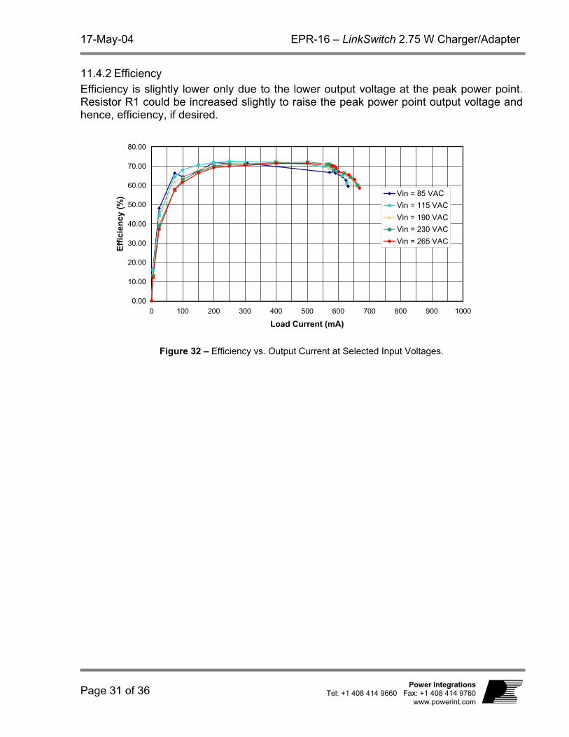
11.4.2 Efficiency Efficiency is slightly lower only due to the lower output voltage at the peak power point. Resistor R1 could be increased slightly to raise the peak power point output voltage and hence, efficiency, if desired.
0.00
10.00
20.00
30.00
40.00
50.00
60.00
70.00
80.00
0 100 200 300 400 500 600 700 800 900 1000
Load Current (mA)
Effic
ienc
y (%
) Vin = 85 VACVin = 115 VACVin = 190 VACVin = 230 VACVin = 265 VAC
Figure 32 – Efficiency vs. Output Current at Selected Input Voltages.
Page 31 of 36 Power Integrations
Tel: +1 408 414 9660 Fax: +1 408 414 9760www.powerint.com

EPR-16 - LinkSwitch 2.75 W Charger/Adapter 17-May-04
11.4.3 No-Load Input Power No-load input power is slightly higher due to the higher no-load voltage. However at 260 mW, the design is still well within the 300 mW specified at 230 VAC.
0
50
100
150
200
250
300
350
80 100 120 140 160 180 200 220 240 260 280
AC Input Voltage (VAC)
Inpu
t Pow
er (m
W)
Figure 33 – Zero Load Input Power vs. Input Line Voltage.
Page 32 of 36 Power Integrations
Tel: +1 408 414 9660 Fax: +1 408 414 9760 www.powerint.com

17-May-04 EPR-16 – LinkSwitch 2.75 W Charger/Adapter
11.5 EMI Performance No change in conducted EMI performance was measured. The results of the LNK520P and modified EP-16 were the same as the original EP-16 design, as shown in Figures 24 and 25. However, the optimized switching characteristics of LNK520P produced a significant reduction in radiated EMI. Figure 34 provides a comparison of quasi-peak radiated emissions with the original EP-16 (LNK501P) and modified EP-16 (LNK520P) designs. A 6 dBµV to 12 dBµV reduction is shown with the LNK520P device. The results are shown as a comparative reference. Actual radiated emissions levels will vary according to radiated test setup and measurement configurations.
LNK501P (EP-16)LNK520P (modified EP-16)
Figure 34 – Comparison of Radiated Emissions, VIN = 230 VAC, 60 Hz Line, Peak Power Point.
Page 33 of 36 Power Integrations
Tel: +1 408 414 9660 Fax: +1 408 414 9760www.powerint.com
EPR-16 - LinkSwitch 2.75 W Charger/Adapter 17-May-04
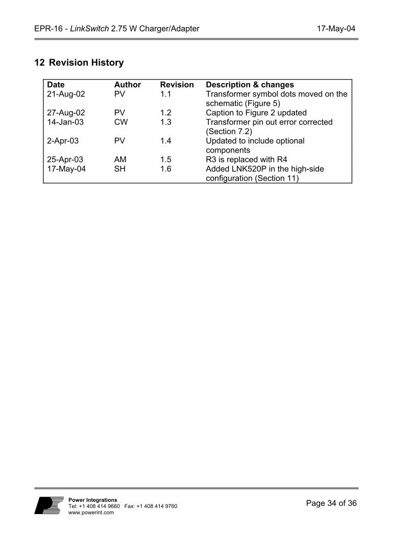
12 Revision History
Date Author Revision Description & changes 21-Aug-02 PV 1.1 Transformer symbol dots moved on the
schematic (Figure 5) 27-Aug-02 PV 1.2 Caption to Figure 2 updated 14-Jan-03 CW 1.3 Transformer pin out error corrected
(Section 7.2) 2-Apr-03 PV 1.4 Updated to include optional
components 25-Apr-03 AM 1.5 R3 is replaced with R4 17-May-04 SH 1.6 Added LNK520P in the high-side
configuration (Section 11)
Page 34 of 36 Power Integrations
Tel: +1 408 414 9660 Fax: +1 408 414 9760 www.powerint.com

17-May-04 EPR-16 – LinkSwitch 2.75 W Charger/Adapter
Notes
Page 35 of 36 Power Integrations
Tel: +1 408 414 9660 Fax: +1 408 414 9760www.powerint.com
EPR-16 - LinkSwitch 2.75 W Charger/Adapter 17-May-04
For the latest updates, visit our Web site: www.powerint.com Power Integrations may make changes to its products at any time. Power Integrations has no liability arising from your use of any information, device or circuit described herein nor does it convey any license under its patent rights or the rights of others. POWER INTEGRATIONS MAKES NO WARRANTIES HEREIN AND SPECIFICALLY DISCLAIMS ALL WARRANTIES INCLUDING, WITHOUT LIMITATION, THE IMPLIED WARRANTIES OF MERCHANTABILITY, FITNESS FOR A PARTICULAR PURPOSE, AND NON-INFRINGEMENT OF THIRD PARTY RIGHTS.
PATENT INFORMATION The products and applications illustrated herein (including circuits external to the products and transformer construction) may be covered by one or more U.S. and foreign patents or potentially by pending U.S. and foreign patent applications assigned to Power Integrations. A complete list of Power Integrations’ patents may be found at www.powerint.com. The PI Logo, TOPSwitch, TinySwitch, LinkSwitch, and EcoSmart are registered trademarks of Power Integrations. PI Expert and DPA-Switch are trademarks of Power Integrations. © Copyright 2004, Power Integrations.
Power Integrations Worldwide Sales Support Locations
WORLD HEADQUARTERS 5245 Hellyer Avenue, San Jose, CA 95138, USA Main: +1-408-414-9200 Customer Service: Phone: +1-408-414-9665 Fax: +1-408-414-9765 e-mail: [email protected]
GERMANY Rueckertstrasse 3, D-80336, Munich, Germany Phone: +49-895-527-3910 Fax: +49-895-527-3920 e-mail: [email protected]
JAPAN Keihin-Tatemono 1st Bldg. 12-20 Shin-Yokohama, 2-Chome, Kohoku-ku, Yokohama-shi, Kanagawa 222-0033, Japan Phone: +81-45-471-1021 Fax: +81-45-471-3717 e-mail: [email protected]
TAIWAN 5F-1, No. 316, Nei Hu Rd., Sec. 1 Nei Hu Dist. Taipei, Taiwan 114, R.O.C. Phone: +886-2-2659-4570 Fax: +886-2-2659-4550 e-mail: [email protected]
CHINA (SHANGHAI) Rm 807, Pacheer, Commercial Centre, 555 Nanjing West Road, Shanghai, 200041, China Phone: +86-21-6215-5548 Fax: +86-21-6215-2468 e-mail: [email protected]
INDIA (TECHNICAL SUPPORT) Innovatech 261/A, Ground Floor 7th Main, 17th Cross, Sadashivanagar Bangalore 560080 Phone: +91-80-5113-8020 Fax: +91-80-5113-8023 e-mail: [email protected]
KOREA 8th Floor, DongSung Bldg. 17-8 Yoido-dong, Youngdeungpo-gu, Seoul, 150-874, Korea Phone: +82-2-782-2840 Fax: +82-2-782-4427 e-mail: [email protected]
UK (EUROPE & AFRICA HEADQUARTERS) 1st Floor, St. James’s House East Street Farnham, Surrey GU9 7TJ United Kingdom Phone: +44-1252-730-140 Fax: +44-1252-727-689 e-mail: [email protected]
CHINA (SHENZHEN) Rm# 1705, Bao Hua Bldg. 1016 Hua Qiang Bei Lu, Shenzhen, Guangdong, 518031, China Phone: +86-755-8367-5143 Fax: +86-755-8377-9610 e-mail: [email protected]
ITALY Via Vittorio Veneto 12, Bresso Milano, 20091, Italy Phone: +39-028-928-6001 Fax: +39-028-928-6009 e-mail: [email protected]
SINGAPORE 51 Newton Road, #15-08/10 Goldhill Plaza, Singapore, 308900 Phone: +65-6358-2160 Fax: +65-6358-2015 e-mail: [email protected]
APPLICATIONS HOTLINE World Wide +1-408-414-9660 APPLICATIONS FAX World Wide +1-408-414-9760
Page 36 of 36 Power Integrations
Tel: +1 408 414 9660 Fax: +1 408 414 9760 www.powerint.com