Simulation-Power Factor Corrector for AC to DC Boost Converter

“POWER FACTOR IMPROVEMENT IN AC-DC CONVERTER”
Major Project report submitted in partial fulfillment of the requirements
For the award of the degree of
BACHELOR OF TECHNOLOGY
IN
ELECTRICAL AND ELECTRONICS ENGINEERING
By
NEEHARIKA.B (08241A0228)
PRIYANKA.V (08241A0231)
ROHINI KEERTI.J (08241A02040)
BHAGYA LAKSHMI.D (09245A0202)
Department of Electrical and Electronics Engineering
GOKARAJU RANGARAJU INSTITUTE OF ENGINEERING
& TECHNOLOGY,
BACHUPALLY, HYDERABAD
2008 – 2012

DEPART NT OF E
CERTIFICATE
This is to certify that the major project report entitledPOWER FACTOR IMPROVEMENT IN AC-DC CONVERTERthat is being submitted by Neeharika.B,Priyanka.V, Rohini Keerti.J,Bhagya Lakshmi.Din partial fulfillment for the award of the Degree of Bachelor of Technology in Electrical and Electronics Engineering to the Jawaharlal Nehru Technological University is a record of bonafide work carried out by them under my guidance and supervision. The results embodied in this project report have not been submitted to any other University or Institute for the award of any Graduation degree.
Mr.P.M.Sarma Mrs.Swathi.DExternal Examiner
HOD, EEE Assistant Professor
GRIET Dept. of EEE
HyderabadGRIET

ACKNOWLEDGEMENT
This is to place on record my appreciation and deep gratitude to the persons
Without whose support this project would ever seen the light of day.
I wish to express my propound sense of gratitude to Mr. P. S. Raju, Director, G.R.I.E.T for his guidance, encouragement, and for all facilities to complete this project.
I also express my sincere thanks to Mr.P.M.Sarma, Head of the Department, G.R.I.E.T and for extending their help.
I have immense pleasure in expressing my thanks and deep sense of gratitude to my guide Mrs.Swathi .D, Assistant Professor, Department of Electrical and ElectronicsEngineering, G.R.I.E.T for his guidance throughout this project.
NEEHARIKA.B (08241A0228)
PRIYANKA.V (08241A0231)
ROHINI KEERTI.J (08241A0240)
BHAGYA LAKSHMI. D(09245A0202)

ABSTRACT
Electronic equipments recently in use ( PCs, TVs, and Telecommunication Equipments
etc.) require power conditioning of some form, typically rectification, for their proper
working. But since they have non-linear input characteristics and they are connected to
the electricity distribution network they produce a non-sinusoidal line current. Current of
frequency components which are multiples of the natural frequency are produced that are
otherwise called the line harmonics. With constantly increasing demand of these kind of
equipments at a high rate, line current harmonics have become a significant problem.
There has been an introduction of a lot of international standards which pose limitations
on the harmonic content in the line currents of equipments connected to electricity
distribution networks. This calls for measures to reduce the line current harmonics,
whichwould improve thePower Factor. There exist two kinds of power factor improvement techniques – passive power factor
improvement and active power factor improvement. In this thesis we tried to devise an
active power factor correction method for improvement of the power factor. UC3845 was
used to design the power factor corrector. This integrated circuit had all the circuits
necessary to control a power factor corrector and was designed to implement the average
current mode control.
i
CONTENTS
1. INTRODUCTION
1.1 Introduction
1.2 Power Factor
1.2.1Forms of Power Factor
1.2.2 Causes of Low Power Factor
2. Power Factor Improvement
2.1 Need of Power Factor Improvement
2.2 Types of Power Factor Improvement
2.2.1 Passive Power Factor Improvement
2.2.2 Active Power Factor Improvement
3. Current Control Mode
3.1 Purpose of Current Control Mode
3.2 Basics of Current Control Mode
3.3 Ideal vs. Real Current Control Mode
3.4 Types of Current Control Mode
3.5 Peak Current Mode Control (PCMC)
3.6 Average Current Mode Control (ACMC)
4. Active power Factor Improvement
4.1 Requisites of Active PFI 4.2 High Power Factor Control Circuit 4.3 Control Circuit for Active Power Factor Improvement
ii

5. Simulation Results 5.1 Multisim result 5.1.1 Testing without IC 5.1.2 Testing with IC 6. Hardware Implementation 6.1 Schematic diagram 6.2 PCB design 6.3 Result 6.4 Hardware Kit
7. Conclusion
7.1 Future scopes
8. Benefits of Power Factor Improvement
9. References
Appendix-A
Appendix-B
Appendix-C
iii

LIST OF FIGURES
Figure 3.1: Block diagram of an ideal current mode converter
Figure 3.2: Scheme of peak current controller
Figure 3.3 Scheme of Average current mode control
Figure 4.1: Basic configuration of a high power factor control circuit
Figure 4.2: Pre-regulator waveforms Figure 4.3: Basic control circuit arrangement necessary for an active power factor Improvement Figure 5.1: Wave form of AC-DC converter without IC Figure 5.2: Waveform of AC-DC converter using IC Figure 6.1: Schematic diagram of AC-DC converter Figure 6.2: PCB design using Eagle software Figure 6.3: Output waveform of converter using IC Figure 6.4: Hardware kit of AC-DC converter
iv
CHAPTER 1 1.1 INTRODUCTION:
An ideal single phase supply for domestic use is given by 230 V, 50 Hz which has a
proper sinusoidal shape. However the power system has impedance which restricts the
flow of current mainly due to magnetic flux effects in substation transformers and
transmission lines. It is not possible to completely avoid this impedance or nullify its
effect to a much lower level. This in turn results in the voltage difference between the
substation supplying power and the consumer point (voltage being less at the consumer
point). On the other front growth of consumer electronics has resulted in increase of
mains driven electronic devices. These devices have mains rectification circuits which is
the main cause of mains harmonic distortion. There would be a lot of such devices and
they would be drawing reactive power from the same supply phase resulting in
significant amount of reactive current flow and generation of harmonics. Both of the above affect the power factor of the transmission system. The former relating
to the impedance affects the displacement power factor while the latter one affects the
distortion power factor of the system. Power factor reveals the electronic usage ratio
which the household electronics consume, mainly focus on the degree of usage and
waste. The better the power factor the better is the degree of power utilization and lesser
is the waste. Hence it is always required to improve the power factor by some means or
other and this project undertaken (Active Power factor Improvement) is an attempt in this
field. In later stages of this report it is explained how this method is adopted and various
advantages of this method over its various counterparts. The project intends to combine
the meritorious features of a boost converter along with the average current control
method.

1.2 POWER FACTOR: In simple terms, power factor can be defined as the ratio of real power to apparent power.
……(1.1) where P is the real input power and Vrms and Irms are the root mean square (RMS)
voltage and current of the load. Correlating to the thesis work these can be considered as
inputs given to the power factor corrector. The power factor is a number between 1 and 0.
When the power factor is not equal to 1, it is an indication that the current waveform does
not follow the voltage waveform. The closer the power factor is to 1 the closer the current
waveform follows the voltage waveform. Real power (watts) produces real work and is known as the energy transfer component.
Reactive power is the power required to produce the magnetic fields (lost power) to
enable the real work to be done. Reactive power comes into action when there is a
mismatch between the demand and supply of power. Apparent power is the total power
that is derived from the power company in order to supply the required power to the
consumer. Although the active power is responsible for doing work, it is from apparent
power only that the current flowing into the load can be determined. In case the load is a pure resistance, only then the real power and the product of the RMS voltage and current will be the same i.e. power factor will be 1. In any other case, the power factor will be below 1. 1.2.1 Forms of Power Factor P ower factor consists of two components:
Displacement power factor Distortion power factor
The displacement power factor is related to the phase angle while the distortion power factor is related to the shape of the waveform.

Power factor = [I rms(1) / I rms ] x cos (Theta) = Kd x Kp ……(1.2) where Irms(1) is the current’s fundamental component and I rms is the current’s RMS
value. Theta is the phase angle displacement between the voltage waveform and the
current waveform. Kd is called as the distortion power factor and Kp is known as the
displacement power factor. If the waveform of both current and voltage are purely sinusoidal, then power factor is
calculated as the cosine of the phase angle between the voltage and current waveforms.
However, in reality always a non-sinusoidal current is drawn by most of the power
supplies. When the current is not sinusoidal and the voltage is sinusoidal, distortion
power factor comes into play which usually is the case. This relationship is shown by
equation 1.2. Displacement power factor comes due to the phase displacement between the current and
voltage waveforms. This displacement is caused by the presence of reactance in the
power supply system. On the other hand harmonic distortion is responsible for distortion
power factor. What happens in reality is the rms value gets increased without any
increase in the amount of power drawn. With increase of these effects the power factor of
the power supply system reduces. These have the effect of pulling the power factor below
the value of 1. 1.2.2 Causes of Low Power Factor The power factor gets lowered as the real power decreases in comparison to the apparent power. This becomes the case when more reactive power is drawn. This may result from increase in the amount of inductive loads (which are sources of Reactive Power) which include - Transformers, Induction motors, Induction generators (wind mill, generators), High intensity discharge (HID) lighting etc. However in such a case the displacement power factor is affected and that in turn affects the power factor. The other cause is the harmonic distortion which is due to presence of the nonlinear loads in the power system. Due to the drawing of non-sinusoidal current there is further reduction in the power factor.

CHAPTER 2
POWER FACTOR IMPROVEMENT Power factor improvement is a modern concept which deals with increasing the degraded
power factor of a power system by use of external equipments. The objective of this
described in plain words is to make the input to a power supply appear as a simple
resistor. As long as the ratio between the voltage and current is a constant the input will
be resistive and the power factor will be 1.0. When the ratio deviates from a constant the
input will contain phase displacement, harmonic distortion or both and either one will
degrade the power factor. In simple words, Power factor improvement is a technique of counteracting theundesirable effects of electric loads that create a power factor ( PF ) that is less than 1. 2.1 NEED OF POWER FACTOR IMPROVEMENT Constant increasing demand of consumer electronics has resulted in that the average
home has a huge variety of mains driven electronic devices. These electronic devices
have mains rectification circuits, which is the dominant reason of mains harmonic
distortion. A lot of modern electrical and electronic apparatus require to convert ac to dc
power supply within their architecture by some process. This causes current pulses to be
drawn from the ac network during each half cycle of the supply waveform. Though a
single apparatus (a domestic television for example) may not draw a lot of reactive power
or it cannot generate enough harmonics to affect the supply system significantly, but
within a typical phase connection there may exist 100s of such devices connected to the
same supply phase resulting in production of a significant amount of reactive current
flow and current harmonics.
With improvement in semiconductor devices field, the size and weight of control circuits
are on a constant decrease. This has also positively affected their performance

andfunctionality and thus power electronic converters have become increasingly popular
in industrial, commercial and residential applications. However this mismatch between
power supplied and power put to use cannot be detected by any kind of meter used for
charging the domestic consumers. It results in direct loss of revenues. Furthermore 3-phase unbalance can also be created within a housing scheme since
different streets are supplied on different phases. The unbalance current flows in the
neutral line of a star configuration causing heating and in extreme cases cause burn out of
the conductor. The harmonic content of this pulsating current causes additional losses and dielectric
stresses in capacitors and cables, increasing currents in windings of rotating machinery
and transformers and noise emissions in many products, and bringing about early failure
of fuses and other safety components. The major contributor to this problem in electronic
apparatus is the mains rectifier. In recent years, the number of rectifiers connected to
utilities has increased rapidly, mainly due to the growing use of computers. Hence it has become very necessary to somehow decrease the effect of this distortion. Power factor correction is an extra loop added to the input of household applications to increase the efficiency of power usage and decrease the degree of waste. 2.2 TYPES OF POWER FACTOR IMPROVEMENT P ower Factor Improvement (PFI) can be classified as two types:
Passive Power Factor Improvement Active Power Factor Improvement
2.2.1 Passive Power Factor Improvement In Passive PFI, only passive elements are used in addition to the diode bridge rectifier, to
improve the shape of the line current. By use of this category of power factor correction,
power factor can be increased to a value of 0.7 to 0.8 approximately. With increase in the
voltage of power supply, the sizes of power factor improvement components increase in
size. The concept behind passive power factor improvement is to filter out the harmonic
currents by use of a low pass filter and only leave the 50 Hz basic wave in order to
increase the power factor.
Passive power factor improvement power supply can only decrease the current wave within the standard and the power factor cannot ever be corrected to 1. And obviously the output voltage cannot be controlled in this case. A dvantages of Passive PFI:
It has a simple structure.
It is reliable and rugged.
In this equipments used don’t generate high-frequency EMI.
Only the construction of a filter is required which can be done easily. Hence the cost is very low.
The high frequency switching losses are absent and it is insensitive to noises and
surges. Disadvantages of Passive PFI:
For achieving better power factor the dimension of the filter increases.
Due to the time lag associated with the passive elements it has a poor dynamic response.
The voltage cannot be regulated and the efficiency is somewhat lower.
Due to presence of inductors and capacitors interaction may take place between the
passive elements or they may interact with the system and resonance may occur at different frequencies.
Although by filtering the harmonics can be filtered out, the fundamental component
may get phase shifted excessively thus reducing the power factor.
The shape of input current is dependent upon the fact that what kind of load is connected.
2.2.2 Active Power Factor Improvement An active PFI is a power electronic system that is designed to have control over the amount of power drawn by a load and in return it obtains a power factor as close as possible to unity. Commonly any active PFI design functions by controlling the input

current of the load in order to make the current waveform follow the mains voltage waveform closely (i.e. a sine wave). A combination of the reactive elements and some active switches are in order to increase the effectiveness of the line current shaping and to obtain controllable output voltage. The switching frequency further differentiates the active PFI solutions into two classes.
• Low frequency active PFI: Switching takes place at low-order harmonics of the line-frequency and it is synchronized with the line voltage.
• High frequency active PFI: The switching frequency is much higher than the line frequency. The power factor value obtained through Active PFI technique can be more than 0.9.
With a suitable design even a power factor of 0.99 can be reached easily. Active PFI
power supply can detect the input voltage automatically, supports 110V to 240V
alternative current, its dimension and weight is smaller than passive PFI power supply
which goes against the traditional view that heavier power supply is better.
A dvantages of Active PFI:
The weight of such a system is very less.
The dimension is also smaller and a power factor value of over 0.95 can be obtained through this method.
Diminishes the harmonics to remarkably low values.
By this method automatic correction can be obtained for the AC input voltage.
It is capable of operating in a full range of voltage.
D isadvantages of Active PFI:
The layout design is bit more complex.
Since it needs PFI control IC, high voltage MOSFET, other circuits; it is highly expensive.

CHAPTER 3
CURRENT CONTROL MODE Current mode control uses the load current as feedback to regulate the output voltage. In this approach there is direct control over the load current whereas output voltage is controlled indirectly, hence it is called "current-mode programming". In this control a functional block using local feedback is formed to create a voltage-to-
current converter. By using this voltage-to-current converter block inside an overall
voltage feedback loop, a voltage regulator can be produced where the control voltage sets
the load current rather than the switch duty cycle (as in the voltage mode programming in
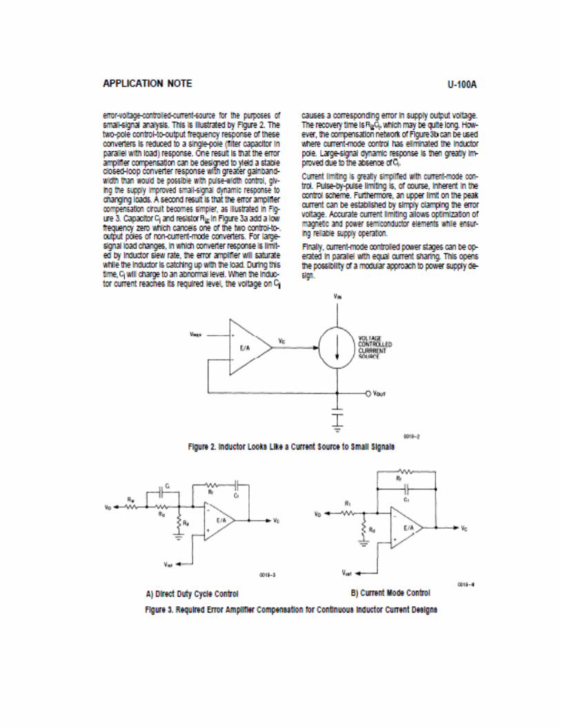
which duty cycle is varied as it is directly proportional to the control voltage). Figure 3.1
is a block diagram of the concept.
Fig 3.1: Block diagram of an ideal current mode converter

3.1 PURPOSE OF CURRENT MODE CONTROL The current-mode approach offers the following advantages:
Since the output current is proportional to the control voltage, the output current can be limited simply by clamping the control voltage.
The energy storage inductor is effectively absorbed into the current source. A simpler compensation network can stabilize the control-to-output transfer function.
When this is applied in higher power applications, parallel connection is used for the power stages. The power stages can be made to share equal current by connecting them to a common bus. This is possible because the output current is proportional to the control voltage.
Last is the automatic feed forward from the line voltage. This particular feature is actually more readily attained in voltage-mode converters by a technique known as "ramp compensation". In fact, in current-mode converters perfect feed forward is obtained only by a particular value of slope compensation.
3.2 BASICS OF CURRENT CONTROL MODE It is a general fact that a constant voltage would be maintained when a constant current
flows through a fixed resistor. But when the load resistor changes to maintain the same
constant voltage, the current level has to change as the load resistance varies. That is
exactly what current mode control of switching power converters is all about. The idea
behind the current mode control is to create a voltage-controlled ideal current source.
This current source is designed in such a way that it maintains a constant voltage at the
output of the power converter regardless of load current changes.
This approach is implemented through two control loops. A current control loop (inner
loop) monitors the information about inductor current and thus creates the voltage-
controlled current source. The other loop is a voltage loop (outer loop) that would
monitor the output voltage of the converter constantly and then program the controlled
current source so as it regulates the output voltage at a given set point.
3.3 IDEAL VS. REAL CURRENT MODE CONTROL However if we consider reality, there is no existence of an ideal voltage-controlled
current source. It is required that the inner current loop senses the inductor current
information and afterwards uses it to turn-on or/and turn-off the power converter
switches. But this process of sensing the current information has time delays associated
with itself and due to it minimum on-time and/or off-time constraints come into picture.
Limitations are imposed by these constraints on the output voltage range that can be generated by a power converter at a given switching frequency and input voltage.
To add to this any sudden change in the load current of the converter would relatively
slow down its response as the inner current loop has a limited bandwidth. Additionally, it
suffers from inherent instabilities, generally referred to as sub-harmonic oscillation. If
adequate compensation is done to account for these instabilities, it slows down the
response to any sudden change in input voltage. These imperfections change the concern
from "seeking ideal performance" to "seeking the best trade-offs for a given application".
This calls for design of different current mode schemes those which can offer the best
trade-off for different applications.
3.4 TYPES OF CURRENT MODE OFCONTROL There are various types of current control schemes. Generally a scheme would be named based on the type of inductor current information being sensed and/or how the information is used to control the power switches. The various current mode control schemes are – average current control, peak current control, hysteresis control, borderline control, valley current control, emulated current control. Out of those many number of schemes average current mode control is being used in the
undertaken project. Hence in this thesis this current control scheme is described
andcomparison with another commonly used current control scheme i.e. peak current
mode control.
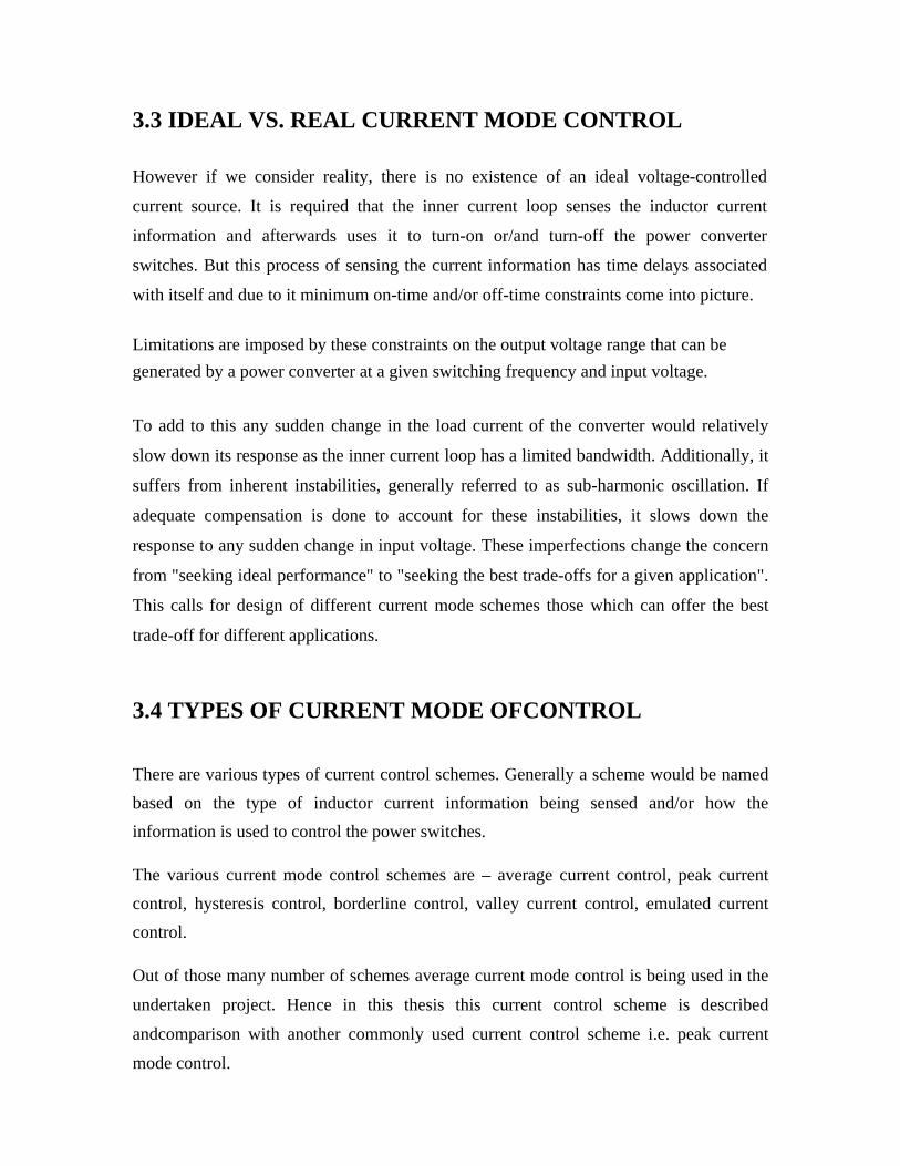
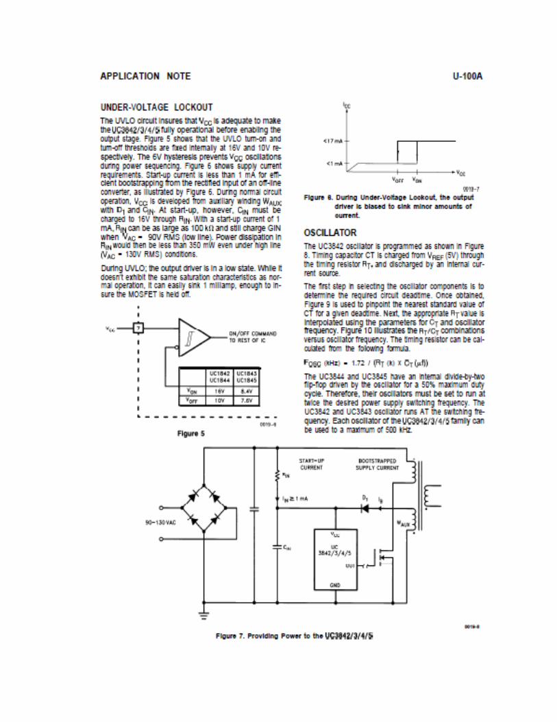
3.5 PEAK CURRENT MODE CONTROL (PCMC) In peak current mode control, the active switch is turned on with constant switching
frequency, and turned off when the upslope of the inductor current reaches a level set by
the outer loop. When the power switch is on it senses the peak inductor current
information, then uses it to turn off the switch. Controlling the turn-off event of the
power switch is commonly referred to as "trailing edge modulation". PCMC offers faster
response to load and line changes, simpler loop compensation requirements, as well as
inherent peak current limit protection as compared to the conventional voltage mode control.
On the other hand, it suffers from sub-harmonic oscillation at duty cycles higher than
50%. By use of ramp compensation which has a slope greater than one-half of the
inductor current down-slope these sub-harmonic oscillations can be damped. However,
this compensation technique may affect this scheme’s response to any sudden change in
load. A time delay is required to sense the peak inductor current somewhat correctly
when the switch is in on state. Hence power converters which utilize PCMC would have
a minimum on-time limitation. This results in imposing a limit on the minimum output
voltage that can be generated by the converter at a given input voltage and switching
frequency.
Fig 3.2: Scheme of peak current controller The above figure represents the scheme of peak current controller along with a typical input.

Advantages of peak current control:
It operates with a constant switching frequency.
A current transformer can sense the switch current and thus losses due to the sensing resistor can be avoided.
Any kind of compensation network or current error amplifier is need not be used
along with it. Possibility of a true switch current limiting.
Response speed and the reliability show improvement. Disadvantages of peak current control:
Sub-harmonic oscillations come into existence at duty cycles greater than 50%, calling for the need of a compensation ramp.
There is input current distortion and it increases with increase in line voltages or with
light load. It further worsens with the use of a compensation ramp.
The control can be affected by commutation changes and are highly sensitive to their presence.
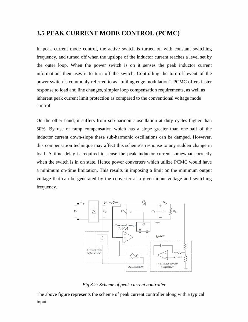
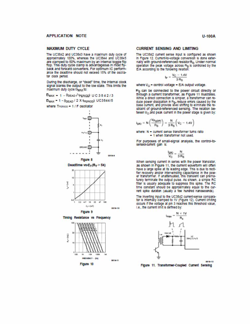
3.6 AVERAGE CURRENT MODE CONTROL (ACMC) In this current mode control scheme the inductor current is sensed and filtered by a
current error amplifier and the output from it drives a PWM modulator. By doing this
extra step the inner current loop minimizes the error between the average input current
and its reference. This latter is obtained in the same way as in the peak current control. Average Current Mode Control is typically a two loop control method (inner loop,
current; outer loop, voltage) for power electronic converters. The main distinguishing
feature of ACMC, as compared with peak current mode control, is that ACMC uses a
high gain, wide bandwidth Current Error Amplifier (CEA) to force the average of one
current within the converter, typically the inductor current, to follow the demanded
current reference with very small error, as a controlled current source. Below in Fig 3.3 the scheme for average current mode control is shown. This technique of average current mode control overcomes the problems of peak current mode control by
introducing a high gain integrating current error amplifier (CEA) into the current loop. The gain-bandwidth characteristic of the current loop can be tailored for optimum
performance by the compensation network around the CA. Compared with peak current
mode control, the current loop gain crossover frequency, can be made approximately the
same, but the gain will be much greater at lower frequencies.
Fig 3.3 Scheme of Average current mode control A dvantages of average current mode control:
It also operates with a constant switching frequency. In this case any compensation ramp is not required.
Since the current is filtered the control is less sensitive to commutation noises unlike
peak current mode control.
Better input current waveforms than for the peak current control since, near the zero crossing of the line voltage, the duty cycle is close to one.

D isadvantages of average current mode control:
The inductor current needs to be sensed which is not easy.
In this current mode control scheme a current error amplifier is needed. For this error amplifier a compensation network needs to be designed in addition, and that must account for different converter operating points
Out of the above two methods the average current mode control is to be implemented in the project due to its superiority over the peak current mode control.
CHAPTER 4
ACTIVE POWER FACTOR IMPROVEMENT 4.1 REQUISITES OF ACTIVE PFI A boost regulator is considered to be the best choice for designing the power stage of the
active power factor corrector. This is because of the continuity of the input current in a
boost converter, production of best input current waveform and the lower level of
conducted. However the high output voltage required in a boost converter accounts as one of its
disadvantage. When design is done for a particular voltage range, the output voltage is
required to be greater than the highest expected peak input voltage. For power factor
correction, the input current in a boost regulator should be made proportional to the input
voltage waveform by some forcing technique or programming. To design such a converter a feedback loop must be implemented to control the input
current. Either peak current mode control or average mode control may be used in these
cases. As discussed earlier peak current mode control has a low gain and a wide
bandwidth current loop which is the reason for its unsuitability for a high performance
power factor corrector, since there is a significant error between the programming signal
and the current. This results in distortion and a power factor worsens more. In average current mode control, to make the input current track the programming signal
with less error an amplifier is used in the feedback loop around the boost power stage.
This is the advantage of average current mode control and it is what makes active power
factor correction possible.

4.2 HIGH POWER FACTOR CONTROL CIRCUIT
A block diagram of a boost power factor corrector is shown in Fig 4.1. The power circuit
of a boost power factor corrector is the same as that of a dc to dc boost converter. A diode
bridge is used to rectify the AC input voltage ahead of the inductor. The capacitor
generally used for this conversion is kept at the output of the converter and even if any
capacitor value is used in the input bridge, its value is very less and it is only used to control any noise.
Fig 4.1: Basic configuration of a high power factor control circuit A constant voltage is obtained at the boost converter output but the input voltage by some
programming forces the input current to be a half wave. The power obtained by the
output capacitor is in the form of a sine wave which has a frequency equal to twice that of
the line frequency and is never constant. This is illustrated in the Fig 4.2. In the figure below, the voltage and current that goes into the power factor corrector are
indicated by the top waveform. The second waveform shows the power that flows into
and out of the capacitor in periods of its charging and discharging. When the input
voltage is higher than the voltage of the capacitor energy is stored in the capacitor. When
the input voltage drops below the capacitor voltage, to maintain the output power flow
the capacitor starts releasing energy. The third waveform in the figure indicates the
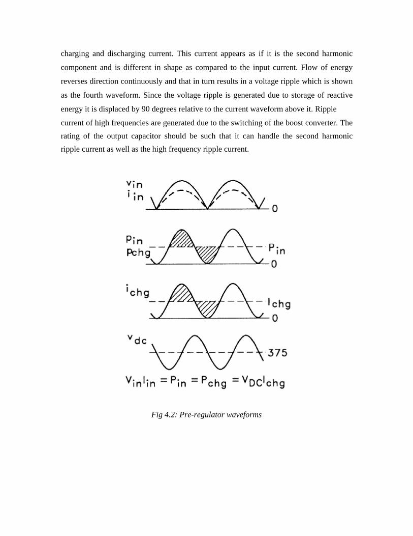
charging and discharging current. This current appears as if it is the second harmonic
component and is different in shape as compared to the input current. Flow of energy
reverses direction continuously and that in turn results in a voltage ripple which is shown
as the fourth waveform. Since the voltage ripple is generated due to storage of reactive
energy it is displaced by 90 degrees relative to the current waveform above it. Ripple
current of high frequencies are generated due to the switching of the boost converter. The rating of the output capacitor should be such that it can handle the second harmonic ripple current as well as the high frequency ripple current.
Fig 4.2: Pre-regulator waveforms
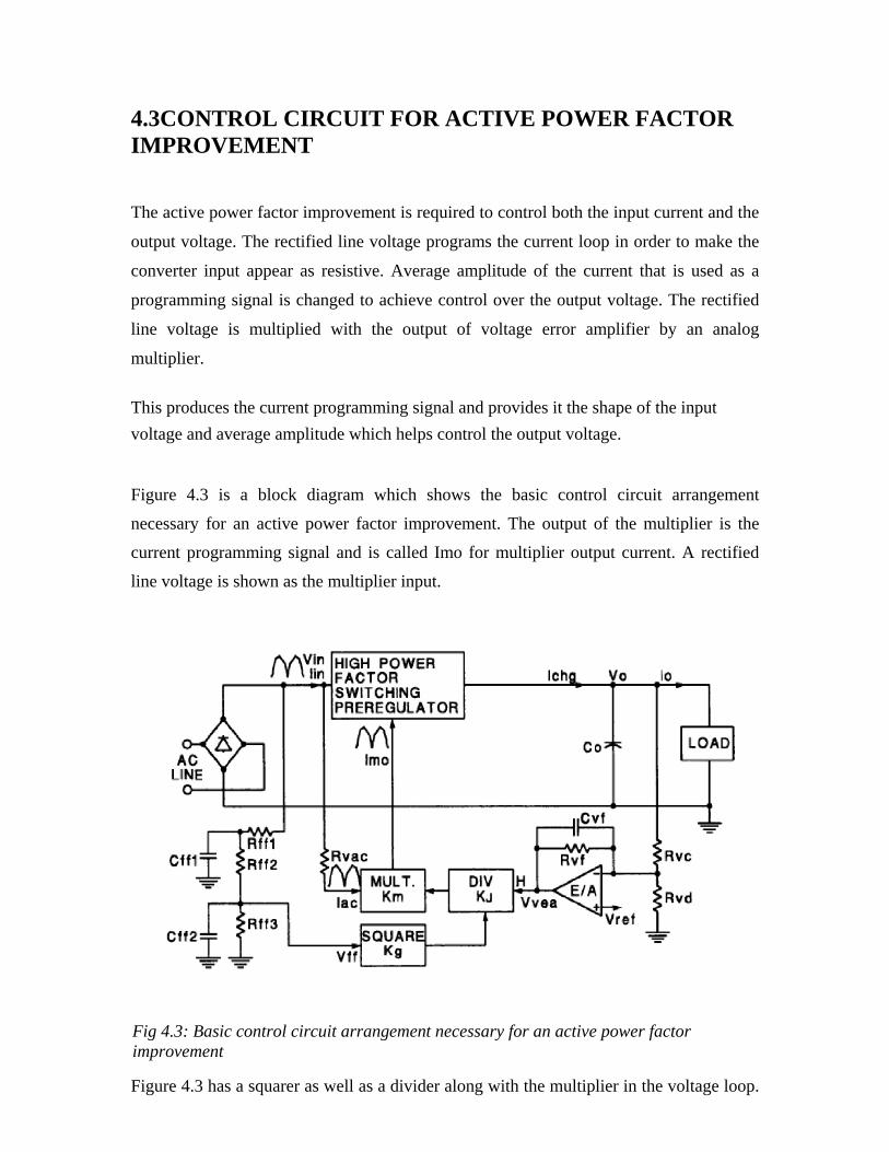
4.3CONTROL CIRCUIT FOR ACTIVE POWER FACTOR IMPROVEMENT
The active power factor improvement is required to control both the input current and the
output voltage. The rectified line voltage programs the current loop in order to make the
converter input appear as resistive. Average amplitude of the current that is used as a
programming signal is changed to achieve control over the output voltage. The rectified
line voltage is multiplied with the output of voltage error amplifier by an analog
multiplier.
This produces the current programming signal and provides it the shape of the input voltage and average amplitude which helps control the output voltage. Figure 4.3 is a block diagram which shows the basic control circuit arrangement
necessary for an active power factor improvement. The output of the multiplier is the
current programming signal and is called Imo for multiplier output current. A rectified
line voltage is shown as the multiplier input. Fig 4.3: Basic control circuit arrangement necessary for an active power factor improvement Figure 4.3 has a squarer as well as a divider along with the multiplier in the voltage loop.
The divider divides the output of the voltage error amplifier by the square of the average
input voltage. The resulting signal is then multiplied by the rectified input voltage signal.
The voltage loop gain is maintained at a constant value due to the presence of the
combination of these blocks. Otherwise the gain would have varied with change in square
of the average input voltage (called feed forward voltage, Vff). This voltage only is
squared by which the output of voltage error amplifier is later divided.
For increasing the power factor to the maximum value possible, the rectified line voltage
and the current programming signal must match as closely as possible. The bandwidth of
the voltage loop should be maintained at a lower value than the input line frequency,
failing which huge distortion is produced in the input current. However on the other hand
for fast transient response of the output voltage the bandwidth needs to be made as large
as possible. In case of wide input voltage ranges, the bandwidth needs to be as close as
possible to line frequency. This is achieved by the action of the squarer and divider
circuits which help maintain the loop gain constant. These circuits that maintain constant loop gain convert the output of voltage error
amplifier into a power control. Hence, now the power delivered to the load is controlled
by this output of the voltage error amplifier. Here we consider an example. Suppose that
the voltage error amplifier output is constant and then we double the input voltage. As the
programming signal depends on the input voltage it will also get doubled. Then it will get
divided by square of the feed forward voltage, which is equal to four times the input now.
This results in reducing the input current to half of its original value. Since the input
voltage is doubled, a factor of two is associated with it. Then it gets multiplied with half
of the input current. This results in no change in the input power and it remains same as
before. The output of the voltage error amplifier, then, controls the input power level of
the power factor improvement. This can be used to limit the maximum power which the
circuit can draw from the power line. Provisions can be made for clamping the output of the voltage error amplifier at some
value which would correspond to some maximum power level. Then as long as the input
voltage is within its defined range, the active power factor improvement will not draw
more than that amount of power.
CHAPTER 5
SIMULATION RESULTS
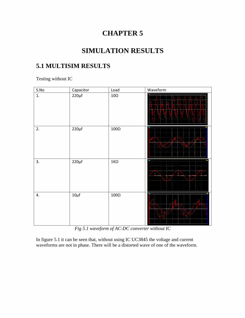
5.1 MULTISIM RESULTS Testing without IC S.No Capacitor Load Waveform 1. 220µf 10Ω
2. 220µf 100Ω
3. 220µf 1KΩ
4. 10µf 100Ω
Fig 5.1 waveform of AC-DC converter without IC In figure 5.1 it can be seen that, without using IC UC3845 the voltage and current waveforms are not in phase. There will be a distorted wave of one of the waveform.
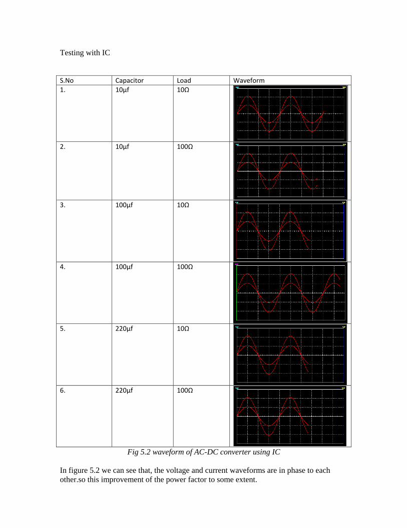
Testing with IC S.No Capacitor Load Waveform 1. 10µf 10Ω
2. 10µf 100Ω
3. 100µf 10Ω
4. 100µf 100Ω
5. 220µf 10Ω
6. 220µf 100Ω
Fig 5.2 waveform of AC-DC converter using IC In figure 5.2 we can see that, the voltage and current waveforms are in phase to each other.so this improvement of the power factor to some extent.
CHAPTER 6
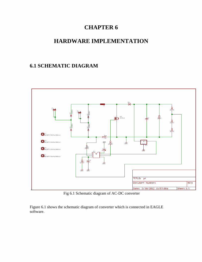
HARDWARE IMPLEMENTATION 6.1 SCHEMATIC DIAGRAM
Fig 6.1 Schematic diagram of AC-DC converter Figure 6.1 shows the schematic diagram of converter which is connected in EAGLE software.

6.2 PCB DESIGN
Fig 6.2:PCB Design using Eagle software
Figure 6.2 shows us the design of PCB of AC-DC converter using EAGLE software.this shows how the design of PCB goes on.
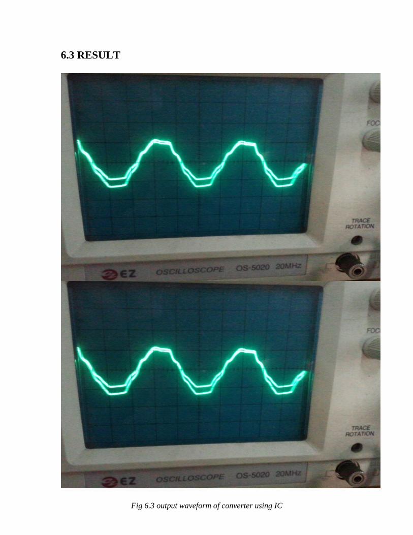
6.3 RESULT
Fig 6.3 output waveform of converter using IC

Figure 6.3 shows the output wave form of AC-DC converter using an IC named UC3845. In the above wave form both the voltage and current waves are in phase.so the difference of angle between them is nearly 0.By this manner we improved the power factor.
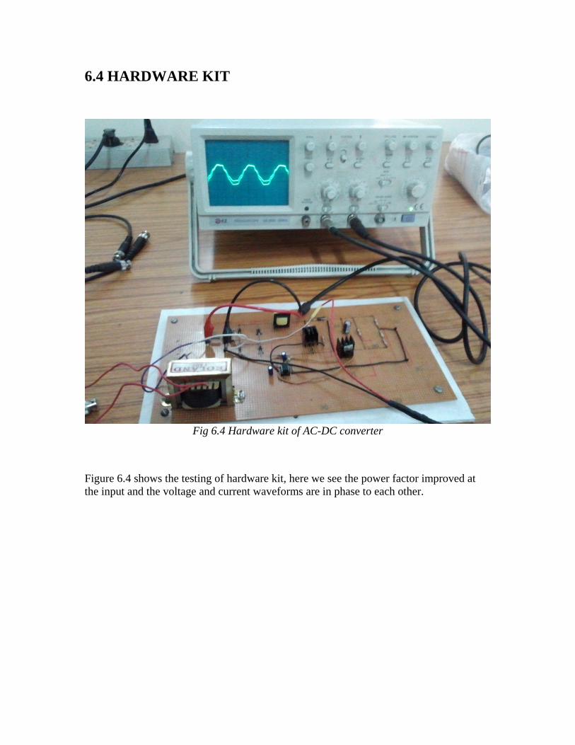
6.4 HARDWARE KIT
Fig 6.4 Hardware kit of AC-DC converter
Figure 6.4 shows the testing of hardware kit, here we see the power factor improved at the input and the voltage and current waveforms are in phase to each other.

CHAPTER 7
CONCLUSION
Power factor improvement counter balances the non-linear loads which account for the low power factor of the system. This technique is of two types active and passive. In the thesis an active power factor technique is proposed. The proposed approach makes a use of UC3845 to design the power factor improvement.This integrated circuit contains the circuits necessary to control a power factor improvement. This UC3845 is designed to implement average current control mode. The power factor can be improved to about 98% by this technique. The use of the inductor on the input side improves the performance of the power factor improvement. 7.1 FUTURE SCOPE Through this thesis analysis of such an active power factor improvement was done by simulations. As a further step, the hardware can be designed and the simulation results can be compared with the results obtained in practical set of conditions.

CHAPTER 8
BENEFITS OF POWER FACTOR IMPROVEMENTATION
There are numerous benefits to be gained through power factor correction. These benefits range from reduced demand charges on your power systemto increased load carrying capabilities in your existing circuits and overall reduced power system loses. And the benefits of power factor correction aren’t just limited to the balance sheet; there are also huge environmental benefits associated with power factor correction, which means your company is reducing its carbon footprint and helping the environment. 1. Reduces demand charges. 2. Increased load carrying capabilities in existing circuits. 3. Improved voltage. 4. Reduced power system losses. 5. Reduced carbon footprint.

REFERENCES: 1. Lessons in Electric Circuits Volume II, Sixth Edition, Tony R. Kuphaldt, 2007 2. Power Factor Correction, Ralph A. Frye III, P.E., http://www.wagesterlease.com/aboutus/articles/powerfactor.html 3. Power Factor, L M Photonics Ltd, http://www.lmphotonics.com/pwrfact.htm?gclid=CJbHjdTMjosCFSUeGAodtRe8VQ
4. "The Active PFC Market is Expected to Grow at an Annually Rate of 12.3% Till 2011" "Higher-powered products are also likely to use active PFC, since it would be the most cost effective way to bring products into compliance with the EN standard."
5.TECHarp: "Power Factor Correction" "Passive PFC ... the power factor is low at 60-80%. ... Active PFC ... a power factor of up to 95%"
6. "Why we need PFC in PSU" "Normally, the power factor value of electronic device without power factor correction is approximately 0.5. ... Passive PFC ... 70~80% ... Active PFC ... 90~99.9%"
7. "PFC options for power supplies" by Tom Brooks 2004 "The disadvantages of passive PFC techniques are that they typically yield a power factor of only 0.60 to 0.70 ... Dual-stage active PFC technology [yields] a power factor typically greater than 0.98"

APPENDIX-A
MultiSIM SOFTWARE NI Multisim (formerly MultiSIM) is an electronic schematic capture and simulation program which is part of a suite of circuit design programs, along with NI Ultiboard. Multisim is one of the few circuit design programs to employ the original Berkeley SPICE based software simulation. Multisim was originally created by a company named Electronics Workbench, which is now a division of National Instruments. Multisim includes microcontroller simulation (formerly known as MultiMCU), as well as integrated import and export features to the Printed Circuit Board layout software in the suite, NI Ultiboard Multisim is widely used in academia and industry for circuits education, electronic schematic design and SPICE simulation. Multisim was originally called Electronics Workbench and created by a company called Interactive Image Technologies. At the time it was mainly used as an educational tool to teach electronics technician and electronics engineering programs in colleges and universities. National Instruments has maintained this educational legacy, with a specific version of Multisim with features developed for teaching electronics.
In 1999, Multisim was integrated with Ultiboard after the original company merged with Ultimate Technology, a PCB layout software company.
In 2005, Interactive Image Technologies was acquired by National Instruments Electronics Workbench Group and Multisim was renamed to NI Multisim.

APPENDIX-B
EAGLE SOFTWARE EAGLE (Easily Applicable Graphical Layout Editor) by Cadsoft is a flexible and expandable EDA schematic capture, PCB layout, autorouter and CAM program widely used since 1988. EAGLE is popular among hobbyists because of its freeware license and rich availability of component libraries on the web.
EAGLE contains a schematic editor, for designing circuit diagrams. Parts can be placed on many sheets and connected together through ports.

APPENDIX-C


39