Power Distribution Network (PDN) Impedance and Target … · 2019-10-22 · Novak, “Comparisonof...
19
Power Distribution Network (PDN) Impedance and Target Impedance Steve Sandler, Picotest Eric Bogatin, Teledyne LeCroy Larry Smith, PDNPowerIntegrity.com
Transcript of Power Distribution Network (PDN) Impedance and Target … · 2019-10-22 · Novak, “Comparisonof...
Power Distribution Network (PDN) Impedance and Target Impedance
Steve Sandler, Picotest
Eric Bogatin, Teledyne LeCroy
Larry Smith, PDNPowerIntegrity.com
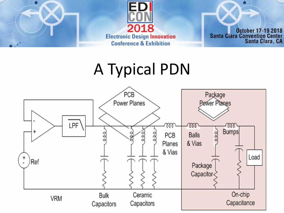
A Typical PDN

Power Integrity Is about managing noise voltage here

Dual(ing) Noise Sources
Load generated
VRM and system generated

Flat Impedance is Ideal, but…
Impedance ignores the VRM generated noise

Single resonant circuit with a “target impedance” of 125mΩ is used to demonstrate the voltage response to a fixed dynamic current amplitude
𝑄 =𝑍𝑜𝑅=22.4𝑚Ω
4𝑚Ω= 5.6
𝑍𝑝𝑘 = 𝑍𝑜 ∙ 𝑄 = 125𝑚Ω
𝑍𝑜=𝐿
𝐶=
50𝑛𝐻
100𝑢𝐹= 22.4𝑚Ω
The Nature of a Peak

𝑉 𝑡 =∆𝐼
𝐶 ∙ 𝜔𝑜2 − 𝛼2
∙ 𝑒−𝛼𝑡 ∙ sin (𝜔𝑜2−𝛼2) 𝑡
Exponential decay
𝑉 𝑠 =1
𝐶∙
∆𝐼
1𝑅𝐶
𝑠 +1𝐿𝐶
+ 𝑠2
Laplace provides the time domain response
Settles to -4mV
Natural Response
Step current ΔI=2Amps
|ΔV| = 43mVpk
STEP PROFILE

𝑉 𝑠 = ∆𝐼 ∙ 𝑄 ∙𝐿
𝐶∙ sin 𝜔𝑜 ∙ 𝑡 − 𝑒
−𝜔𝑜2𝑄𝑡 ∙ sin( 𝜔𝑜
2 −𝜔𝑜2𝑄
2
) 𝑡
Exponential growth
Note: Q is now in the numerator
|ΔV|=124mVpk
Forced Response
Sine current ΔI=2Amps
RESONANT SINE

2
𝑇න0
𝑛𝜋
𝐴 ∙ 𝑠𝑖𝑛 𝑛𝑡 𝑑𝑡 + න𝑛𝜋
2𝑛𝜋
𝐴 ∙ 𝑠𝑖𝑛 𝑛𝑡 𝑑𝑡 =4
𝑛𝜋=1.273
𝑛
The Fourier transform of a square wave at any harmonic, n
27% larger than sine excitation
4 ∙ 124𝑚𝑉
𝜋= 158mVpk
|ΔV|=158mVpk
Forced Response
Square current ΔI=2Amps
RESONANT SQUARE

The Two responseThis oscilloscope screenshot shows both the natural (step) response and the forced (resonant square wave) response at the same time.
The exponential decay, exponential growth and impact of resonant Q are all clear here.

Three resonances, each with a peak impedance of 125mΩ
Most PDNs exhibit more thanone resonant peak
What will the excursion be for a ΔI of 2A?
Multiple Resonances

Creating a worst case current pattern results in a voltage response of 586mVpk.
The excursions were all excited and phased to sum –resulting in a Rogue wave.
This is more than 10X the response to a single 125mΩpeak step response.
∆𝑽𝒓𝒐𝒈𝒖𝒆≈ ∆𝑰
𝟎
𝒏
𝒁𝒊)
Rogue Waves

Target Impedance
𝑉𝑝𝑘−𝑝𝑘 = 𝐼𝑝𝑘−𝑝𝑘 ∙4 ∙ 𝑍𝑝𝑘
𝜋
For a single Impedance peak
𝑍𝑡𝑎𝑟𝑔𝑒𝑡 =𝑉𝑝𝑘−𝑝𝑘
𝐼𝑝𝑘−𝑝𝑘∙𝜋
4
Solving for an equivalent impedance Target Impedance Bandwidth
𝑍𝐵𝑊 =0.35
𝑡𝑒𝑑𝑔𝑒
But beware of additional resonances and noise sources!

Dynamic Current is Complicated
When the core activity starts it appears as both a step and also as high frequency content
When the activity stops it appears as a step.
The exponential decay is clear and the response is asymmetric
< 146 mV

Forced Response
When the core activity is at a repetition rate that matches the die resonant peak, we can see the much larger forced response.
We can’t see the exponential growth in this picture
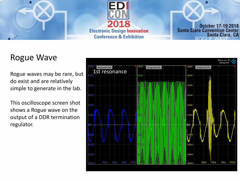
Rogue Wave
1st resonance
2nd resonance ROGUE WAVE
Rogue waves may be rare, but do exist and are relatively simple to generate in the lab.
This oscilloscope screen shot shows a Rogue wave on the output of a DDR termination regulator.

Conclusions
1. Target impedance is a tool that helps design a robust PDN that results in acceptable noise2. While flat impedance is ideal, careful management of the peaks can result in an acceptable
design3. Keep in mind that the VRM and system also generate noise that will appear at the die4. Multiple sources are additive.

Thanks for Attending Our Session!
Maintain your Integrity - Power Responsibly

1. Larry D. Smith, Eric Bogatin, “Principles of Power Integrity for PDN Design--Simplified: Robust and
Cost Effective Design for High Speed Digital Products” (Prentice Hall Modern Semiconductor Design),
ISBN-13: 978-0132735551, April 6, 2017
2. Sandler, S, “Power Integrity: Measuring, Optimizing, and Troubleshooting Power Related Parameters in
Electronics Systems”, Nov 18, 2014
3. W. Cheng, A. Sarkar, S. Lin, and Z. Zheng, “Worst case switching pattern for core noise analysis,”
DesignCon, 2009.
4. S. Sun, L. D. Smith, and P. Boyle, “On-chip PDN noise characterization and modeling,” DesignCon,
2010.
5. L. D. Smith, S. Sun, P. Boyle, and B. Krsnik, "System power distribution network theory and
performance with various noise current stimuli including impacts on chip level timing,” in Proc. Custom
Integrated Circuits Conference, San Jose, CA, 2009.
6. I. Novak, “Comparison of power distribution network design methods: Bypass capacitor selection based
on time domain and frequency domain performances”. Manuscript for TF-MP3 “Comparison of Power
Distribution Network Design Methods” at DesignCon 2006, February 6-9, 2006, Santa Clara, CA
7. C. K. Cheng “Power Distribution Network Simulation and Analysis” UCSD March, 4, 2010
8. Hu, Xiang, Peng Du, and Chung-Kuan Cheng. "Exploring the rogue wave phenomenon in 3D power
distribution networks." Electrical Performance of Electronic Packaging and Systems (EPEPS), 2010
IEEE 19th Conference on. IEEE, 2010.
REFERENCES