Privacy-Aware Ant Colony Optimization Algorithm for Real ...

Power-Aware System-on-Chip Test Optimization through Frequency andVoltage Scaling
by
Vijay Sheshadri
A dissertation submitted to the Graduate Faculty ofAuburn University
in partial fulfillment of therequirements for the Degree of
Doctor of Philosophy
Auburn, AlabamaMay 4, 2014
Keywords: System-on-Chip, Test Schedule Optimization, Voltage and Frequency Scaling,Session-Based Test Schedule, Sessionless Test Schedule
Copyright 2014 by Vijay Sheshadri
Approved by
Prathima Agrawal, Samuel Ginn Distinguished Professor of Electrical and ComputerEngineering
Vishwani D. Agrawal, James J. Danaher Professor of Electrical and Computer EngineeringAdit Singh, James B. Davis Professor of Electrical and Computer Engineering

Abstract
A System-on-Chip (SoC) is a complete system that has been integrated onto a single
chip. An SoC is often designed by embedding reusable blocks called cores. With shrinking
device sizes, SoC cores are growing in number and complexity, which has led to high volumes
of test data and resulted in long test times. Therefore, reducing test cost by minimizing the
overall test time is one of the main goals of System-on-Chip (SoC) testing. Power dissipation
during test mode is often much higher than that of functional mode and hence, test power
management is also a major concern in SoC testing. To efficiently manage test resources
and power dissipation, tests for the SoC cores are arranged into test schedules. Within these
test schedules, the core tests may (as in the case of session-based test schedule) or may
not (as in the case of sessionless test schedule) be grouped into test sessions. Traditional
SoC test methods assume a constant test frequency and supply voltage (VDD) for the entire
test schedule. However, test time and test power can be regulated by VDD and test clock
frequency to optimize SoC test schedules for a given power budget.
The research presented in this dissertation focuses on power-aware optimization of SoC
test schedules to minimize test time by scaling the supply voltage and test clock rate. This
scaling can be session wise (in the case of a session-based test schedule) or dynamic (in
case of sessionless test schedule). SoC testing can be sped up by increasing the test clock
rate. However, test clock is constrained by the rated power limit (power constraint) and
the critical path delay (structure constraint) of the SoC cores. These constraints can be
manipulated using VDD. Therefore, by scaling VDD and clock rate, an optimal test time and
schedule can be obtained for an SoC.
For the session-based test scheduling, the optimization problem is mathematically for-
mulated and solved through Integer Linear Program (ILP) based methods to provide optimal
ii

solutions. For SoCs with large number of cores, Integer Linear Programs are NP-hard and,
in general, computationally expensive. To overcome this difficulty, a simulated annealing
based heuristic method capable of providing near-optimal solutions is developed. Results
show that the overall SoC test time can be considerably shortened by scaling the test clock
and supply voltage. A similar heuristic method that is based on simulated annealing algo-
rithm, is developed for the optimization of sessionless test schedules. The heuristic approach
is capable of both preemptive (tests can be halted and resumed at will) and non-preemptive
scheduling (tests cannot be interrupted at any time). Here also, the optimization results
show a significant test time reduction over conventional reference test schedules where VDD
and clock are fixed at given nominal values.
iii

Acknowledgments
There are many people to whom I would like to express my gratitude for their help during
the pursuit of my doctoral dreams. Foremost among them are Professors Prathima Agrawal
and Vishwani D. Agrawal, without whose constant support and guidance this dissertation
would not have been possible.
I would like to thank Dr. Adit Singh, for serving as a member of my advisory committee,
and Dr. Sanjeev Baskiyar, the external reader for this dissertation. I am also thankful to
Dr. Victor Nelson, for teaching me the various VLSI-CAD tools through his course ‘CAD
for VLSI’. Thanks are in order, as well, for Dr. Alice Smith and Dr. Chase Murray from the
Dept. of Industrial Engineering. I have immensely benefited from their courses on Adaptive
Optimization and Linear Programming. I would also like to acknowledge the support of
Ms. Shelia Collis and the Wireless Engineering Research and Education Center (WEREC),
Ms. Jo Ann Loden, Ms. Penny Christopher and Ms. Carol Lovvorn in helping me keep my
school and immigration paper work in order.
My heartfelt thanks go out to my colleagues in Broun Hall, in particular, Dr. Pratap
Prasad, Dr. Santosh Kulkarni, Dr. Suraj Sindia, Praveen Venkataramani, Gopalkrishna
Iyer and Muralidharan. I owe much gratitude to all my friends, especially to the Auburn
Kannada Koota gang.
Above all, I would like to express my deepest gratitude to my caring parents and my
loving wife for their constant love compassion and support.
Finally, I must acknowledge that the research presented in this dissertation, is supported
in part by the National Science Foundation Grants CCF-1116213, IIP-0738088 and IIP-
1266036.
iv

Table of Contents
Abstract . . . . . . . . . . . . . . . . . . . . . . . . . . . . . . . . . . . . . . . . . . . ii
Acknowledgments . . . . . . . . . . . . . . . . . . . . . . . . . . . . . . . . . . . . . . iv
List of Figures . . . . . . . . . . . . . . . . . . . . . . . . . . . . . . . . . . . . . . . vii
List of Tables . . . . . . . . . . . . . . . . . . . . . . . . . . . . . . . . . . . . . . . . ix
1 Introduction . . . . . . . . . . . . . . . . . . . . . . . . . . . . . . . . . . . . . . 1
1.1 Problem Statement . . . . . . . . . . . . . . . . . . . . . . . . . . . . . . . . 2
1.2 Organization of Dissertation . . . . . . . . . . . . . . . . . . . . . . . . . . . 3
2 Background and Prior Work on SoC Testing . . . . . . . . . . . . . . . . . . . . 4
2.1 Test Infrastructure . . . . . . . . . . . . . . . . . . . . . . . . . . . . . . . . 5
2.1.1 Core Test Wrapper . . . . . . . . . . . . . . . . . . . . . . . . . . . . 6
2.1.2 Test Access Mechanism (TAM) . . . . . . . . . . . . . . . . . . . . . 7
2.2 Test Scheduling . . . . . . . . . . . . . . . . . . . . . . . . . . . . . . . . . . 7
2.3 Power Constrained Testing . . . . . . . . . . . . . . . . . . . . . . . . . . . . 9
2.4 Frequency and Voltage Scaling . . . . . . . . . . . . . . . . . . . . . . . . . . 10
3 Optimization of Session-Based Test Schedules . . . . . . . . . . . . . . . . . . . 12
3.1 Background . . . . . . . . . . . . . . . . . . . . . . . . . . . . . . . . . . . . 12
3.2 Mixed-Integer Linear Program (MILP) Based Optimization . . . . . . . . . . 18
3.2.1 Introduction . . . . . . . . . . . . . . . . . . . . . . . . . . . . . . . . 18
3.2.2 MILP Formulation . . . . . . . . . . . . . . . . . . . . . . . . . . . . 19
3.3 Heuristic Based Optimization . . . . . . . . . . . . . . . . . . . . . . . . . . 21
3.3.1 Simulated Annealing (SA) . . . . . . . . . . . . . . . . . . . . . . . . 21
3.4 Results . . . . . . . . . . . . . . . . . . . . . . . . . . . . . . . . . . . . . . . 25
3.4.1 Experimental Setup . . . . . . . . . . . . . . . . . . . . . . . . . . . . 25
v

3.4.2 MILP Results . . . . . . . . . . . . . . . . . . . . . . . . . . . . . . . 27
3.4.3 Heuristic Algorithm Results . . . . . . . . . . . . . . . . . . . . . . . 30
3.4.4 Lower Bounds on SoC Test Time . . . . . . . . . . . . . . . . . . . . 31
3.4.5 SoC Power Budget . . . . . . . . . . . . . . . . . . . . . . . . . . . . 33
3.4.6 Multiple Supply Voltages . . . . . . . . . . . . . . . . . . . . . . . . . 35
4 Optimization of Sessionless Test Schedules . . . . . . . . . . . . . . . . . . . . . 36
4.1 Heuristic Approach to Optimization . . . . . . . . . . . . . . . . . . . . . . . 36
4.2 Optimization Results . . . . . . . . . . . . . . . . . . . . . . . . . . . . . . . 38
4.2.1 Lower Bound on SoC Test Time . . . . . . . . . . . . . . . . . . . . . 42
4.2.2 SoC Power Budget . . . . . . . . . . . . . . . . . . . . . . . . . . . . 43
4.2.3 Multiple Supply Voltages . . . . . . . . . . . . . . . . . . . . . . . . . 44
4.3 Comparison With Session-Based Testing . . . . . . . . . . . . . . . . . . . . 45
5 Conclusion and Future Work . . . . . . . . . . . . . . . . . . . . . . . . . . . . . 50
5.1 Future Work . . . . . . . . . . . . . . . . . . . . . . . . . . . . . . . . . . . . 53
Bibliography . . . . . . . . . . . . . . . . . . . . . . . . . . . . . . . . . . . . . . . . 54
Appendix: SoC Test Benchmarks . . . . . . . . . . . . . . . . . . . . . . . . . . . . . 59
vi

List of Figures
2.1 A simple test set-up showing the SoC under test, the test source and sink. The
test data from the test source to different cores and from the cores to the test
sink, is carried over the test bus. . . . . . . . . . . . . . . . . . . . . . . . . . . 4
2.2 SoC Test scheduling modeled as 3D optimization problem. . . . . . . . . . . . . 5
2.3 Overview of IEEE1500 wrapper [40]. (WBR = wrapper boundary register; WBY
= wrapper bypass; WP(I/O) = wrapper parallel (input/output); WS(I/O) =
wrapper serial (input/output); WIR = wrapper instruction register.) . . . . . . 6
2.4 Two test scheduling strategies, session-based (non-partitioned) and sessionless(partitioned)
are illustrated. Sessionless testing can be non-preemptive (b) or preemptive (c)
[33,35]. . . . . . . . . . . . . . . . . . . . . . . . . . . . . . . . . . . . . . . . . 8
2.5 Test time as a function of VDD [65]. The nominal and the optimal VDD are
denoted by Vnom and Vsync, respectively. . . . . . . . . . . . . . . . . . . . . . . 11
3.1 Overview of the SA heuristic algorithm. . . . . . . . . . . . . . . . . . . . . . . 22
3.2 Generating the initial solution for the SA algorithm. . . . . . . . . . . . . . . . 23
3.3 Components of ASIC Z and their test time (in arbitrary units) and test power
(in mW). . . . . . . . . . . . . . . . . . . . . . . . . . . . . . . . . . . . . . . . 25
3.4 CPU time (in seconds) of the MILP optimization method for the ITC benchmarks. 30
vii

3.5 CPU time (in seconds) of the heuristic optimization method for the SoC bench-
marks. . . . . . . . . . . . . . . . . . . . . . . . . . . . . . . . . . . . . . . . . . 32
4.1 ‘Merging’ test sessions to convert a session based test schedule into a sessionless
test schedule. . . . . . . . . . . . . . . . . . . . . . . . . . . . . . . . . . . . . . 37
4.2 The ‘Merge’ function erases the session boundaries in a session based test schedule
and combines the tests together to form a sessionless test schedule. . . . . . . . 38
4.3 Best-fit decreasing (BFD) algorithm for sessionless test scheduling. Test schedules
obtained from this algorithm are used as reference cases in this paper where
voltage and frequency are fixed at their nominal values for the entire schedule. . 39
4.4 Convergence of the SA based optimization algorithm. The plot shows the heuris-
tic algorithm converging towards the optimum test time as the temperature pa-
rameter (T ) reduces. . . . . . . . . . . . . . . . . . . . . . . . . . . . . . . . . . 40
4.5 Optimized sessionless test schedules for ASIC Z, under non-overlapping voltage
range condition, for both (a) non-preemptive and (b) preemptive cases. (Note:
Diagram not to scale.) . . . . . . . . . . . . . . . . . . . . . . . . . . . . . . . . 45
4.6 Comparing session-based and sessionless test schedules. . . . . . . . . . . . . . . 47
viii

List of Tables
3.1 Test Data set for ASIC Z at nominal supply voltage (1.0V) . . . . . . . . . . . . 26
3.2 Optimized Test Schedule for ASIC Z for nominal and custom clock rate (Cases1 and 2). The supply voltage is at nominal value for both cases. . . . . . . . . . 28
3.3 Test times (in arbitrary units) of ASIC Z system for custom VDD and clock rate(Case 3). . . . . . . . . . . . . . . . . . . . . . . . . . . . . . . . . . . . . . . . 29
3.4 Test times (in arbitrary units) for benchmark SoCs, obtained by MILP optimiza-tion method for the three optimization cases considered. . . . . . . . . . . . . . 29
3.5 Test times (in arbitrary units) for MILP and heuristic test scheduling methods,with customized VDD and clock rates. . . . . . . . . . . . . . . . . . . . . . . . 30
3.6 Test times (in arbitrary units) for benchmark SoCs, obtained by the heuristicoptimization method for the three optimization cases considered. . . . . . . . . 31
3.7 Optimal test times (in arbitrary units) for nominal and custom clock rate (Cases1 and 2) compared with the lower bound on test time at nominal VDD. . . . . . 33
3.8 Optimal test times (in arbitrary units) for custom VDD and clock frequency (Op-timization Case 3) compared with the lower bound on test time at Vmin. . . . . 34
3.9 Optimized test times (in arbitrary units) for ASIC Z, for various power budgetvalues. . . . . . . . . . . . . . . . . . . . . . . . . . . . . . . . . . . . . . . . . . 34
3.10 Test times (in arbitrary units) and optimal voltages of ASIC Z system, for dualvoltage ranges. . . . . . . . . . . . . . . . . . . . . . . . . . . . . . . . . . . . . 35
4.1 Test times (in arbitrary units) for sessionless test scheduling with voltage andfrequency scaling. . . . . . . . . . . . . . . . . . . . . . . . . . . . . . . . . . . . 41
4.2 CPU times∗ for all the benchmarks SoCs for the heuristic optimization algorithm. 42
4.3 Test times (in arbitrary units) for sessionless test scheduling with voltage andfrequency scaling. . . . . . . . . . . . . . . . . . . . . . . . . . . . . . . . . . . . 43
4.4 Sessionless test schedule optimization for ASIC Z, subject to various power budgetvalues. . . . . . . . . . . . . . . . . . . . . . . . . . . . . . . . . . . . . . . . . . 44
ix

4.5 Comparing test time results for session-based and sessionless test schedule opti-mization. . . . . . . . . . . . . . . . . . . . . . . . . . . . . . . . . . . . . . . . 46
4.6 Comparison of CPU times between session-based and sessionless testing, for theheuristic optimization algorithm. . . . . . . . . . . . . . . . . . . . . . . . . . . 48
1 Overview of the benchmarks used in this dissertation. . . . . . . . . . . . . . . . 60
x

Chapter 1
Introduction
Technological developments have made it possible to integrate an entire system onto
a single chip. Termed as ‘System-On-Chip’ (or SoC for short), these devices have core
based architecture where each core is often a reusable logic or memory block. Owing to
their modularity, small area, high performance and low power consumption, SoC devices are
becoming increasingly popular. In recent times, SoCs are extensively used in networking and
communication applications. Emerging cellular and wireless technologies, such as WiMAX
and LTE require high data rates, low latency at very low power budgets. SoCs are well suited
for such requirements as they offer low power, programmable and cost-effective hardware
solutions. SoCs are the driving force behind modern-day smart phones and tablets, and can
also be found in other wireless applications such as radios, wireless access points, Bluetooth,
etc.
The number of cores being embedded in SoC devices is increasing due to device size
miniaturization. The resulting complexity and increase in the number of fault-sites has com-
plicated testing of SoCs. Consequentially, the test data volume also grows in proportion
to the number of cores in the SoC, since each core is associated with one or more tests,
leading to longer test times. Thus, test time minimization has become a major challenge
in the field of SoC testing. While testing multiple cores simultaneously can reduce the test
time significantly, such concurrent execution is limited by excessive power dissipation due
to increased switching activity. The power dissipation of a circuit during test mode is often
higher than functional mode. Elevated power levels and heat dissipation by neighbouring
cores can lead to the formation of thermal hotspots and undesirable power droops. Ther-
mal hotspots may eventually cause irreversible damages to the chip whereas power droops
1

induce clock stretching which may lead to a good chip incorrectly failing a timing test [18].
Therefore, power-aware test strategies are needed for efficient test power management.
1.1 Problem Statement
The complexity of SoC testing is mitigated to an extent by adopting modular testing,
which is equivalent to a “divide-and-conquer” approach. In modular testing, block-level tests
can be applied to individual blocks (cores) of the SoC, such that these blocks can be tested
almost independent of one another. As discussed earlier, concurrent testing of cores presents
a trade-off between test time and test power. Hence, an optimal arrangement of core tests
can be formed so as to yield a minimal test time while maintaining the test power under a
safe limit. Such an arrangement is termed as SoC test schedule (discussed in detail in the
next chapter).
The general SoC test scheduling problem can be stated as: Given an SoC with N cores,
where each core may be associated with one or more tests, and a test power budget, find a
test schedule (concurrency and sequence of test application) to:
a. Test all cores.
b. Reduce the overall test time.
c. Conform to the SoC test power budget.
The contribution of this work is a power-aware test scheme that optimizes the overall
test time of an SoC by exploiting the influence of VDD and clock over test power and test time
of individual cores. In this work, both exact and heuristic approaches for test optimization
are provided; while the exact method provides the most optimal result, the heuristic method
achieves near-optimal results but addresses the problem of scalability.
2

1.2 Organization of Dissertation
The rest of this dissertation is organized as follows: Chapter 2 discusses the basics of
SoC testing methodologies and summarizes the previous work in this field. Optimization
techniques for SoC test schedules are presented in Chapters 3 and 4. Chapter 5 concludes
the research work presented in this dissertation. The details of the SoC benchmarks, used
in this research work, are provided in the appendix.
3

Chapter 2
Background and Prior Work on SoC Testing
As mentioned previously, in SoC testing, the modularity of an SoC is exploited by
treating each core as a testable unit. A simple test set-up for an SoC is shown in Figure 2.1.
The test source stores and provides the test stimuli for all the cores. The test bus relays the
stimuli to the corresponding core and the test response of the cores to test sink. The test
sink stores all responses which are then compared to the response of a fault-free version of
the device to identify the faults.
Figure 2.1: A simple test set-up showing the SoC under test, the test source and sink. Thetest data from the test source to different cores and from the cores to the test sink, is carriedover the test bus.
It is easily seen that as the number of cores increases, the overall test time of the SoC
also increases. While concurrent testing of cores may cut down the overall test time, there
may be other factors influencing it. For instance, there may be some test resources, such as
test bus, external pins of the SoC, etc., that may be commonly shared among cores. This
may lead to a conflict when such cores are tested simultaneously. Test power may also limit
concurrent testing of cores.
The SoC testing problem can be modeled as a 3-dimensional optimization problem,
where the SoCs power limit, test time and resources (such as pin count, etc.) form the three
4

Figure 2.2: SoC Test scheduling modeled as 3D optimization problem.
axes. The power limit is fixed for the SoC and the resources have a limited availability. The
objective of the 3-D optimization would be to minimize the test time by effective allocation
of resources such that the power limit is not exceeded. This optimization problem has been
modeled as a 3-D bin packing problem [24] as shown in Figure 2.2. Each core in the SoC
can be modeled as a cuboid, where the core’s test power, test time and test resources, such
as BIST resources, wrapper width, etc., constitute the three dimensions. The idea here is
to place the cores in the cuboid representing the SoC in such a way that the test time is
minimized while satisfying the power and resource constraints. This bin packing problem
differs from the general bin packing problem in that if two cores are tested simultaneously,
they overlap only on the time axis and not on the other two axes.
2.1 Test Infrastructure
The test infrastructure of SoC consists of a wrapper and a test access mechanism
(TAM) [7].
5

Figure 2.3: Overview of IEEE1500 wrapper [40]. (WBR = wrapper boundary register; WBY= wrapper bypass; WP(I/O) = wrapper parallel (input/output); WS(I/O) = wrapper serial(input/output); WIR = wrapper instruction register.)
2.1.1 Core Test Wrapper
The test wrapper aides in the access and isolation of embedded cores. It acts as an
interface between the core and the on-chip structure for test data transportation (TAM).
The IEEE 1500 standard for embedded cores defines a standardized, scalable and configurable
core wrapper for both logic and memory cores [1]. This wrapper consists of scan and control
registers, data and control signals and instruction set. The IEEE 1500 wrapper architecture
is shown in Figure 2.3. The boundary registers (WBR) form the wrapper chains which
interface the TAM with the internal scan chains through the parallel pins (WPI/WPO).
The instruction register (WIR) provides the necessary control information.
The wrapper may also perform serial-parallel or parallel-serial conversion to provide
width adaptation in case of a mismatch between the available TAM width and the core
input/output terminals. Wrapper configuration can be optimized for effective utilization of
test bandwidth [20,21,31,35,39,47,48].
6

2.1.2 Test Access Mechanism (TAM)
TAM is the infrastructure responsible for transporting the test data between SoC ex-
ternal pins and embedded cores. The TAM can be dedicated solely for test purposes or can
be an existing on-chip bus structure. TAM design involves trade-offs between the transport
capacity of the mechanism and the test application cost incurred in terms of test time, area
overhead, etc.
Multiple TAM architectures have been proposed in the past. Aerts and Marinissen
introduce [5]:
• A multiplexing architecture, where the entire TAM width is allocated to each core and
the cores are tested sequentially,
• A distributed architecture, where a fixed TAM width is assigned to each core,
• A daisy chain architecture, where all the TAM width is assigned to every core but a
bypass structure is added to shorten the access path for the cores.
More recently, a flexible TAM architecture has been proposed, where the TAM assignement
to the cores is flexible; hence the TAM varies dynamically after each core test [26,27,71].
Previously published work formulates the test time as a function of TAM width and
optimizes TAM allocation among cores, to achieve test time minimization. It has been
shown [27] that the relation between the test time and TAM width is that of a ’staircase’
function, meaning that the test time will only reduce after the TAM assignment to a core ex-
ceeds a certain core threshold value. Some of the published references on TAM optimization
are [25–27,34,48,71].
2.2 Test Scheduling
As mentioned earlier, a test schedule is an ordered arrangement of core tests often
optimized for lowering test time and/or test power. A simple test schedule can be sequential
7

Figure 2.4: Two test scheduling strategies, session-based (non-partitioned) and session-less(partitioned) are illustrated. Sessionless testing can be non-preemptive (b) or preemptive(c) [33,35].
or concurrent. In sequential scheduling, only one core is tested at a time. As a result,
the overall test time is simply the sum of all individual core test times. While this is the
simplest scheme to implement, the overall test time is longest. Concurrent scheduling, on
the other hand, makes use of concurrency by simultaneously testing multiple cores. Existing
concurrent scheduling strategies may be broadly categorized into:
• Session-based (non-partitioned) test scheduling, where no new test is allowed to start
until all tests of a previous session are completed. A test session refers of a set of tests
initiated simultaneously and run concurrently [13,14,35,55,56,73]. See the illustration
in Figure 2.4(a).
• Sessionless (partitioned) test scheduling, where test session boundaries are ignored and
a test may be scheduled to start as soon as possible [23,44,54,57,58,74]. The sessionless
or partitioned test scheduling can be further divided into preemptive and non preemp-
tive scheduling. In the preemptive strategy, tests can be interrupted or restarted at
8

any time [25,34]. The non preemptive strategy does not allow such interruptions, i.e., a
test once initiated must be completed. Figures 2.4(b) and (c) illustrate non-preemptive
and preemptive schedules, respectively.
2.3 Power Constrained Testing
To be used during test mode, the test vectors are so designed as to maximize switching
activity in the circuit, in order to detect more faults per vector and hence minimize the test
time. Therefore, test power can be up to four times the functional power [68]. To guarantee
that this increased power dissipation will not cause heat induced failures in the device, a
peak power budget for the entire SoC is defined. Power constrained test scheduling focuses
on optimizing the overall test time of the SoC for a given power budget.
Many power-constrained testing strategies have been studied in the past [13, 14, 18, 25,
34, 53, 55, 56, 71]. The concept of fixing a single power budget for the SoC is known as
the global peak power model and has been widely used. However, this model is regarded
as a pessimistic approach since the single power limit value is based on the peak power
consumption of the circuit and the circuit’s power consumption may not often reach peak
power. Samii et al. proposed a cycle-accurate power model where there is a power value for
every clock cycle [52]. While this model is more accurate than the global peak power model,
it is more complex and computationally expensive. Alternatively, Larsson [32] proposed a
power grid model aimed at countering local hot spots. This model allocates cores to a set
of power grids. During test scheduling, cores are selected such that not only the global peak
power limit, but also the grid’s power limit is not exceeded.
In the research presented in this dissertation, we adopt a global peak power model where
the power consumption during simultaneous execution of multiple tests is given by the sum
of their peak powers, and this value must not exceed the peak power budget of the SoC at
any given time. The additive model for estimating power consumption was introduced by
9

Chou et al. [13,14]. In this model, the test power consumption of a block is approximated to
a single value corresponding to the peak power consumption over the test time of the block.
2.4 Frequency and Voltage Scaling
The idea of scaling voltage and frequency has been prevalent in the field of microproces-
sors and SoCs. In [60], a locally placed configurable dynamic voltage and frequency scaling
(DVFS) controller enables a large number of on-chip processors to switch VDD by selecting
from two power grids and also independently controls their clock rates, in order to improve
the energy efficiency of the multi-processor SoC (MPSoC). Voltage and frequency scaling
techniques have also been employed in testing of SoCs.
Recently, multi-frequency SoC testing has been investigated. Sehgal et al. [53] have fo-
cused on the use of a multi-channel ATE capable of providing multiple frequencies. Zhao et al.
[70] discuss test optimization through wrapper design in order to perform bandwidth match-
ing between the ATE’s clock input and the core’s frequency. The PMScan system, introduced
by Devanathan et al. [16], utilizes an adaptive supply voltage regulation scheme that lowers
the VDD to balance the power dissipation and the frequency during the shift operation, while
satisfying the timing requirements. Scheduling with multiple voltage islands and testing of
cores at multiple voltages has also been considered [29]. These authors schedule core tests at
multiple voltage levels and clock domains and reduce the clock frequency during low voltage
testing to enable a time division multiplexing scheme for concurrent testing of cores.
Venkataramani et al. [62–66] discuss two aspects of testing, namely, power constrained
testing where the test clock speed is limited by the circuit’s rated power and structure
constrained testing where the test clock speed is limited by the critical path or other timing
constraints of the circuit. The supply voltage is used for the purpose of balancing these two
constraints to allow higher test clock rates in order to achieve test time reduction. Since
test power is two to four times higher than the functional power, test clock is often power
constrained, i.e., any increase in the clock would cause the power to exceed the device’s rated
10

Figure 2.5: Test time as a function of VDD [65]. The nominal and the optimal VDD aredenoted by Vnom and Vsync, respectively.
maximum. The power consumption can be reduced by lowering the operating voltage. As a
result, the clock rate can be increased without exceeding the power constraint of the core.
However, reducing the voltage causes the delay of a circuit to increase, hence, elongating
the critical path of the device. Thus, as we reduce VDD, on one hand, the lowered power
consumption allows higher clock rates thereby shrinking the test time but, on the other
hand, the increased circuit delay requires slower clock rate and a longer test time. As
Figure 2.5 [62, 64, 65] shows there exists an optimal point where the two constraints are
satisfied and at the same time test time is significantly reduced. Experiments on ISCAS
benchmark circuits by those authors show test time reductions of up to 62% at optimal
values of VDD [63].
11

Chapter 3
Optimization of Session-Based Test Schedules
3.1 Background
Objectives of SoC testing, as outlined previously, are to test all cores of the SoC while
managing the power dissipation so as to avoid thermal stress. Consider an SoC with n cores
C1, · · · , Cn, where each core Ci is associated with a test ti, and a peak power budget. The
power budget for an SoC, Pmax, is defined as the maximum allowable power dissipation
during the testing of SoC. The power budget is chosen so as to account for power droops and
thermal hotspots that may occur due to peak activity during testing. Let there be n cores,
C1, · · · , Cn in an SoC and let the test corresponding to a core Ci be ti, where i ∈ 1, 2, · · · , n.
Each test is associated with test time and test power, which have been characterized at
nominal operating conditions (nominal voltage and clock rate). Let Tti and Pti be the time
and power of the test ti. Let tests, t1,· · · , tn, be distributed among k sessions, S1, · · · ,
Sk such that each session, Sj contains one or more tests. The test time of a session Sj,
given by TSj= max(Tti |∀ti ∈ Sj) and the power dissipated during session, Sj is given by
PSj=
∑(Pti),∀ti ∈ Sj.
The general test scheduling problem can be expressed as an optimization problem:
Objective:
Minimizek∑j=1
TSj.xj
where xj =
1, if Sj is scheduled
0, otherwise
12

Subject to:
1) Power constraint: PSj.xj ≤ Pmax, Pmax being the power budget for the SoC.
2) Test completeness constraint: each test, ti, i ∈ {1, 2, · · · , n} is executed at least once.
The test time and test power can, however, be influenced by the test clock. A faster clock
reduces the test time but increases the power consumption. Lowering the clock frequency,
on the other hand, reduces the test power but leads to longer test time. Thus, there exists
a trade-off between the test time and test power. However, the energy spent during testing
remains constant. Energy spent per core test, Eti = Pti ×Tti . The total energy spent during
the testing of the entire SoC can then be expressed as, Etotal =n∑i=1
Pti × Tti . In [62, 64, 65],
the authors have proved that a lower bound on the total test time is given by the ratio of
the total energy spent during the test and the power budget,
TTLB1 =EtotalPmax
=
n∑i=1
Pti × TtiPmax
=n∑i=1
PtiPmax
Tti , (3.1)
where TTLB1 is the lower bound on SoC test time.
LetPmaxPti
= Fti , where Fti is the scaling factor by which the clock frequency of a test ti is
varied with respect to the nominal value. This scaling factor shall be referred to as frequency
factor for the remainder of this work. Hence, the total test time of an SoC is lowest when
each core test is scheduled sequentially at a clock rate equal to Pmax
Ptifnom.
Theorem 3.1 Concurrent scheduling of core tests at a test clock rate Pmax
Ptifnom, cannot
improve the lower bound on the total test time of the SoC, obtained by the sequential test
schedule at the same clock rate.
Proof: Let there be n tests, t1, · · · , tn. Let Tti and Pti be the test, ti’s test time and power
dissipated, respectively. Let Pmax be the power budget.
Case 1: Sequential test scheduling (One test scheduled per session).
13

Let each session Si contain a single test, ti. This implies that the session’s test time and
power are the same as that of the test, i.e., TSi= Tti = Ti and PSi
= Pti = Pi. Now, if
the clock frequency is altered, for speeding up the testing, the frequency factor, Fi =Pmax/Pi.
The modified session test time, now, is Ti/Fi or, Ti.Pi/Pmax. The total test time (say TT1),
therefore, isn∑i=1
Ti.Pi/Pmax or,
TT1 = (T1.P1 + · · ·+ Tn.Pn)/Pmax (3.2)
Case 2: Concurrent test scheduling (Multiple tests scheduled in each session).
Let the n tests be scheduled in k sessions such that every test is covered by exactly one test
session. The test time and power of a session, Sj are given by TSj= max{Ti} and PSj
=∑(Pi),∀ti ∈ Sj, respectively. If the clock frequency per session is varied, the frequency factor
per session, Fj = Pmax/PSj= Pmax/
∑Pi,∀ti ∈ Sj. The modified session test time for
session, Sj is given by, (max{Ti}.∑Pi)/Pmax,∀ti ∈ Sj. The total test time (say TT2),
therefore, is [k∑j=1
TSj(∑Pi)]/Pmax, ∀ti ∈ Sj or,
TT2 = [TS1 .(P1 + · · ·+Px) + · · ·+ TSk.(Py + · · ·+Pn)]/Pmax,where x, y ∈ {1, · · · , n} (3.3)
For any session, Sj, TSj≥ Ti,∀ti ∈ Sj, i.e, the session’s test time is always greater than or
equal to the test times of the tests in that session. This implies that, if tests tx, ty, tz ∈ Sj,
then TSj.Px +TSj
.Py +TSj.Pz ≥ Tx.Px +Ty.Py +Tz.Pz. The LHS of this inequality resembles
3.3 and the RHS resembles that of 3.2. Hence, from this and 3.2 and 3.3, we can say that
TT2 ≥ TT1 and therefore, the total test time of concurrent scheduling is at most as small
as the lower bound when the test clock rate is Pmax
Ptifnom.
The test power of a core test, characterized at nominal supply voltage (Vnom), is de-
pendent on voltage. As E ∝ P ∝ V 2, the energy per core test and hence the total test
energy also varies with the supply voltage. Therefore, the lower bound on test time given in
14

Equation 3.1 is applicable at the nominal supply voltage. The energy per core test is given
by, Eti = Pti(Vmin
Vnom)2Tti , where Vmin is the lowest value to which the supply voltage can be
reduced, without disrupting the circuit’s functionality. Hence, the new lower bound for the
total test time of the SoC is,
TTLB2 =
n∑i=1
Pti(Vmin
Vnom)2Tti
Pmax, (3.4)
where TTLB2 is the new lower bound on SoC test time.
Note that here a constant Vmin is assumed for all SoC cores; however, the value of Vmin may
vary among the cores.
The theorem showed that scheduling core tests at a clock frequency such that the power
consumed per test is the same as the power budget, yields the lower bound and that con-
current test scheduling cannot improve this lower bound. This is under the assumption that
the power dissipation of a core can be raised to equal the power budget without any phys-
ical limitation on the individual core power limit or the clock. In reality, the clock rate of
individual cores is often limited by their structural constraints (e.g., critical path delay) and
power constraints(rated maximum power). Consequentially, the maximum clock frequency
of a session is decided by the maximum clock frequency of the slowest core in that session,
i.e., f(Sj) ≤ min{fmax(ti)|∀ti ∈ Sj} , where f(Sj) is the clock rate of session Sj and fmax(ti)
is the maximum clock frequency of a test ti. Since all cores of the SoC are tested at the
nominal clock frequency, fnom, it is valid to assume that fnom is the clock rate of the slowest
core in the SoC (say f0). Then, frequency factor of a session, Fj = f(Sj)
f0. Note that the test
session containing the slowest core of the SoC will possess a unity frequency factor. The
maximum frequency factor is given by:
max{Fj} = min[min{fmax(ti)|∀ti ∈ Sj}
f0,PmaxPSj
] (3.5)
15
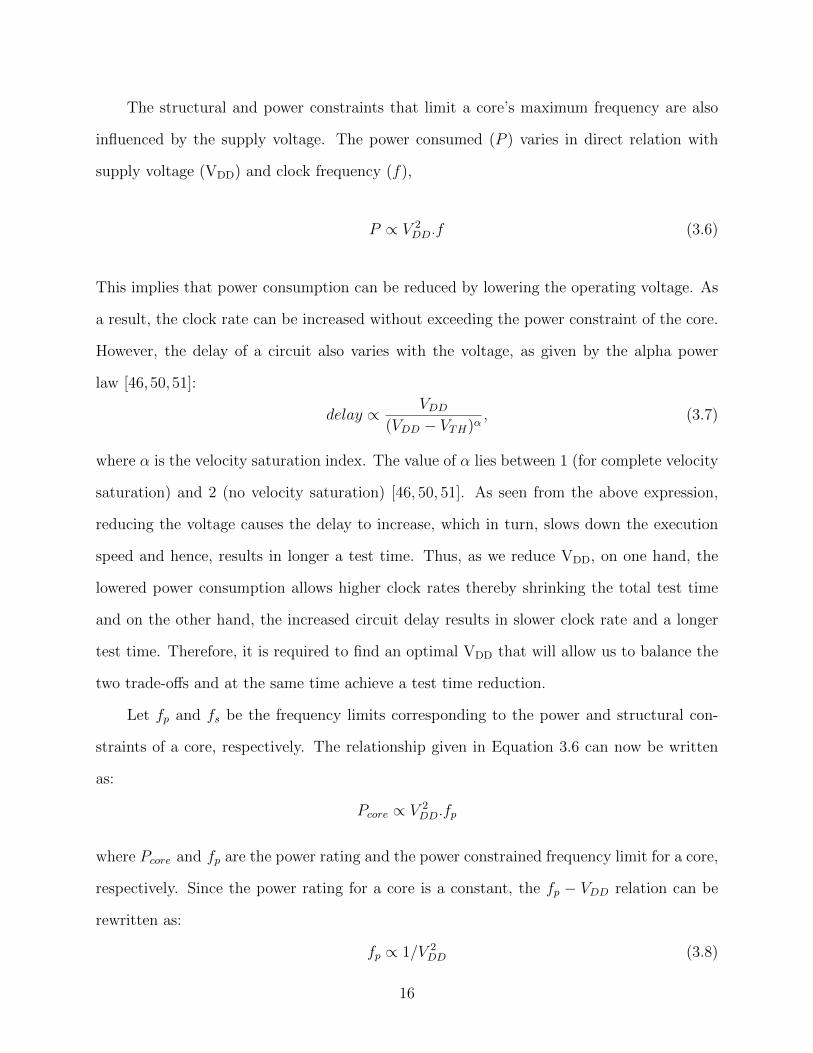
The structural and power constraints that limit a core’s maximum frequency are also
influenced by the supply voltage. The power consumed (P ) varies in direct relation with
supply voltage (VDD) and clock frequency (f),
P ∝ V 2DD.f (3.6)
This implies that power consumption can be reduced by lowering the operating voltage. As
a result, the clock rate can be increased without exceeding the power constraint of the core.
However, the delay of a circuit also varies with the voltage, as given by the alpha power
law [46,50,51]:
delay ∝ VDD(VDD − VTH)α
, (3.7)
where α is the velocity saturation index. The value of α lies between 1 (for complete velocity
saturation) and 2 (no velocity saturation) [46, 50, 51]. As seen from the above expression,
reducing the voltage causes the delay to increase, which in turn, slows down the execution
speed and hence, results in longer a test time. Thus, as we reduce VDD, on one hand, the
lowered power consumption allows higher clock rates thereby shrinking the total test time
and on the other hand, the increased circuit delay results in slower clock rate and a longer
test time. Therefore, it is required to find an optimal VDD that will allow us to balance the
two trade-offs and at the same time achieve a test time reduction.
Let fp and fs be the frequency limits corresponding to the power and structural con-
straints of a core, respectively. The relationship given in Equation 3.6 can now be written
as:
Pcore ∝ V 2DD.fp
where Pcore and fp are the power rating and the power constrained frequency limit for a core,
respectively. Since the power rating for a core is a constant, the fp − VDD relation can be
rewritten as:
fp ∝ 1/V 2DD (3.8)
16

The fs−VDD relationship can be expressed, in accordance with the alpha power law (Equa-
tion 3.7), as:
fs ∝(VDD − VTH)α
VDD(3.9)
From these expressions it can be noted that as VDD is decreased, fp increases allowing higher
clock rates. At the same time, fs decreases with decreasing VDD, thus restricting the clock
rate. Both these constraint limits are independent of each other, i.e., the power constraint
limit fp is only decided by the rated power of the core, with no regards to the critical path
of the core and similarly, the critical path of the core dictates the structure constraint limit,
ignoring the rated power limit of the core. The maximum clock rate of a core, therefore, is
the minimum of the two frequency limits. Now, the clock frequency of a session, which is
the same as the slowest core in that session, is given by f(Sj) ≤ min{fp(ti), fs(ti)|∀ti ∈ Sj}
and since the frequency factor of a session, Fj = f(Sj)
f0, its maximum value is given by,
max{Fj} = min[min{fp(ti), fs(ti)|∀ti ∈ Sj}
f0,PmaxPSj
] (3.10)
The lower bound for the SoC test time, defined in Equation 3.4, does not take into
account, the structure constraint of the clock rate. As a result, the equation predicts that
the test time continually reduces as VDD is lowered. However, from Figure 2.5, we know
that beyond an optimal VDD point, the test time increases with decreasing VDD. Therefore,
Equation 3.4 is revised to include the optimal voltage, Vopt, instead of Vmin.
TTLB2 =
n∑i=1
Pti(VoptVnom
)2Tti
Pmax, (3.11)
It can be noted that Equation 3.4 would be the same as Equation 3.11, when Vopt = Vmin.
Let us assume that fs = k · fp at Vnom. As VDD is lowered, both fs and fp vary
accordingly. At Vopt, fs(Vopt) = fp(Vopt), i.e., fs · Vnom
Vopt· ( Vopt−Vth
Vnom−Vth)α = fp · (Vnom
Vopt)2. Since
17

fs/fp = k,
k =VnomVopt
· (Vnom − VthVopt − Vth
)α (3.12)
The value of α for recent short-channel MOSFETs is 1.3 [50]. For the sake of simplicity, let
us assume the value of α as 1. Now, Equation 3.12 can be written as, k(Vopt)2 − kVthVopt −
Vnom(Vnom − Vth) = 0, which is of the form ax2 + bx+ c = 0. Solving for Vopt,
Vopt =kVth ±
√(kVth)2 + 4kVnom(Vnom − Vth)
2k(3.13)
3.2 Mixed-Integer Linear Program (MILP) Based Optimization
3.2.1 Introduction
Linear Programming (LP) [28] is an optimization tool designed to achieve the best
outcome in a mathematical model where the relationship among the factors involved in the
model can be formulated as linear equalities or inequalities. Linear programming consists
of a linear objective function that has to be optimized under restrictive conditions that are
expressed as linear equalities or inequalities. The canonical form of LP problems is:
maximize cTx
Subject to Ax ≤ b and x ≥ 0
where c and b are vectors of constant coefficients and A is a matrix of pre-determined
coefficients whereas x is a vector of variables (known as decision variables) whose values are
to be determined.
Integer linear programming (ILP) is a special case of linear programming wherein all
the variables are restricted to integers. ILP problems are NP-complete and hence, large
optimization problems are intractable through this method. Similar to ILP, MILP (mixed
integer linear programming)is also a special case of linear programming since it contains
a combination of integral and real-valued decision variable. MILP problems are also NP-
complete and solving them can be cumbersome and time consuming. In the past, MILP
18

based optimization techniques have been used for SoC test scheduling [8–10, 27, 29]. The
MILP model presented in this section takes into account the influence of VDD and clock on
the test time and test power and optimizes the overall test time of the SoC for a pre-defined
peak power limit.
3.2.2 MILP Formulation
The mixed-ILP model for optimizing VDD and clock rate per test session is formulated
in this section. The voltage range is divided into multiple steps of voltages and for each step,
the test power and frequency limits (structure and power constraint) of each test session is
pre-computed. Let Pij be the test power of jth session at ith voltage. Similarly, let Fsij and
Fpij be the frequency limit imposed by the structure and power constraints, respectively,
for the jth session at ith voltage. For each session, the VDD is chosen by a binary variable
whereas the clock rate of the session is a real-valued variable. Tj and Fj are the test time
and frequency factor of a test session. xij is a binary variable that selects a test session
and its optimal VDD among all possible test sessions and voltage steps. The test schedule
optimization can then be described as follows:
Objective:
Minimize∑i,j
(Tj/Fj).xij,
where xij =
1, if jthsession is scheduled at ithvoltage
0, otherwise
Subject to:
1. Fj.∑i
(Pij.xij) ≤ Pmax
2.∑ixij = 1
3. a. Fj.xij ≤ Fsij b. Fj.xij ≤ Fpij
19

4. each test, ti, i ∈ {1, .., n} is executed at least once.
The first constraint of the ILP ensures that the power consumption of the test session does
not exceed the power budget. The second constraint specifies that each session should be
associated with exactly one voltage value. The clock frequency is bounded by the structure
constraint (Fsij) and the power constraint (Fpij) in the ILP’s third constraint. The fourth
one is a test completeness constraint which ensures that all the core tests are scheduled.
The above non-linear model is linearized using simple substitutions. Let 1/Fj = uj and
uj.xij = qj,∀i, j. These substitutions necessitate the inclusion of two more constraints: 1)
qj ≥ uj −M(1− xij),∀i, j, where M is a large number such that M >> uj, 2) qj ≥ 0 . The
new ILP formulation is as follows:
Objective:
Minimize∑jTj.qj,
Subject to:
1.∑i
(Pij.xij) ≤ Pmax.uj
2.∑ixij = 1
3. a. xij ≤ Fsij .uj b. xij ≤ Fpij .uj
4. each test, ti, i ∈ {1, .., n} is executed at least once.
5. qj ≥ uj −M(1− xij),∀i, j
6. qj ≥ 0
Note that the voltage step size determines the precision of the solution. However,
reducing the step size to enhance the precision would increase the number of variables in the
formulation and hence render the problem intractable through ILP.
20

3.3 Heuristic Based Optimization
Integer Linear Programs are NP-hard, in general and are computationally expensive for
large SoCs. The CPU time required to obtain an optimal solution increases exponentially as
the number of cores and the complexity of the SoC increases. The proposed MILP method
also shares the same issues with scalability in terms of the problem size. Hence, a simulated
annealing (SA) based optimization technique is presented that is much faster than ILP for
larger SoCs and also capable of producing results similar to that of the ILP method. Heuristic
algorithms, often employing greedy approaches, perform much better in terms of CPU time
as compared to exact methods such as ILP. While a heuristic method does not guarantee
an optimal solution, a good algorithm can produce near-optimal values consistently. Many
heuristic optimization approaches in the field of SoC testing have been published in the
past [15, 19,23,35,44,57,74].
3.3.1 Simulated Annealing (SA)
Simulated annealing is a directed search algorithm inspired from the annealing process
in metallurgy, first proposed by Kirkpatrick et al. [30] has been used in the past for SoC
test scheduling [23, 35, 74]. The algorithm accepts a non-improving solution with a finite
probability so as to avoid getting stuck at a local optimum. The probability of accepting
worse solutions is controlled by the temperature parameter (T ). As the temperature of the
process cools down, it becomes less and less likely for the algorithm to accept non-improving
solutions. Theoretical studies on simulated annealing have shown that simulated annealing
based algorithms converge to a global optimum with a probability of 1 under certain specified
conditions on the updating and iteration of temperature values [61]. The overview of our
SA based optimization algorithm is as shown in Figure 3.1.
21

Simulated Annealing HeuristicT = temperatureK = cooling parameterTf = final temperatureXB = best solution obtained so farXC = current solution
generate initial solution, X0 (test schedule and corresponding test time)XB = X0, XC = X0
while T ≥ Tf doperform SA move operation (swapping of tests) on XC
scale clock rate and voltage to optimize the new test schedulecompute test time of the optimized test schedule, Xnew
Diff = Xnew −XC
if Diff ≤ 0 or exp(−DiffKT ) ≥ random(0, 1) thenXB = Xnew, XC = Xnew
elsediscard Xnew and retain XC
end if
T = K × T
end while
Figure 3.1: Overview of the SA heuristic algorithm.
Initial solution
The initial solution is developed by inserting a randomly selected test into a session
until the session’s power consumption (Pses) is close to the peak power budget (Pmax). This
step is repeated until all the tests are grouped into sessions such that no two sessions contain
the same test.
The test schedule, thus generated, serves as the starting point for the simulated anneal-
ing heuristic. Frequency and voltage scaling (described in Cost Calculation) are also applied
to optimize the test time obtained through Figure 3.2.
SA move operator
The move operator in our simulated annealing algorithm is a swapping of tests between
two sessions. Among the many test sessions of the test schedule, two sessions s1 and s2 are
22

Initial Solutionlist1 = list of core tests to be scheduled {initially contains all core tests}list2 = list of core tests currently executed {initially empty}tsch = 0 {overall test time of the test schedule}while list1 is not empty do
list2 = empty listwhile Pses < Pmax do
insert random test i into list2delete test i from list1Pses = ΣPi, ∀i ∈ list2
end whileif Pses > Pmax then
remove recently added test from list2end iftsch = tsch + max(ti,∀i ∈ list2)
end while
Figure 3.2: Generating the initial solution for the SA algorithm.
selected at random, such that s1 6= s2. A randomly chosen test in each session is swapped
with each other, thus forming a new test schedule. The cost of the resultant solution, which
is the test time of the new test schedule, is computed. The new test schedule is accepted if
the new solution is better than the best solution obtained so far or if their difference (d) is
such that exp( −dKT
) ≥ random(0, 1), where K is the cooling parameter and T is the annealing
temperature (described in Annealing Schedule), else the swap is discarded.
Simulated annealing is a neighborhood evaluation based class of algorithms where neigh-
boring solutions are examined and accepted or discarded. The neighboring solutions, in this
case, are obtained by swapping of the tests in the sessions. In the worst case, the number
of sessions may be the same as the number of tests implying that each session will contain
one unique test. Hence, the number of neighboring solutions for an SoC with ‘n’ core tests
would ben(n− 1)
2.
Cost calculation
The cost in this optimization problem refers to the test time of the test schedule. The
overall test time for the session-based test schedule is the sum of the test time of the longest
23

test in the session. The test clock frequency and the supply voltage are scaled to optimize
the test time. The scaling factor for the clock, referred to as the frequency factor (F), is
updated after addition of every test during the initial solution phase and after every swap,
in the SA move operation phase. The frequency factor is limited by both the peak power
budget and the clock rate constraints of individual core of the SoC, as given in Equation 3.5.
Voltage scaling is done for each session as given below:
• reduce VDD by one step.
• Calculate the power and structure constraint limits of the tests using Equations 3.8
and 3.9 respectively.
• Update the frequency factor using Equation 3.10.
• Repeat the steps if the resulting session test time is lower than before, else quit the
voltage scaling procedure.
Annealing schedule
Annealing schedule refers to the temperature (T ), the cooling parameter (K ) and their
effects on the optimization procedure. True to the metallurgical annealing process, the initial
value of the temperature is high. Each iteration of the heuristic, which produces a new
solution, corresponds to a value of the temperature. After each iteration, the temperature
is reduced according to Tnew = K × T , where K ≤ 1. Hence, the number of iterations is
dependent on both, the temperature and the cooling parameter. The stopping criteria for
the procedure would be the temperature value reducing below a certain specified limit.
24

Figure 3.3: Components of ASIC Z and their test time (in arbitrary units) and test power(in mW).
3.4 Results
3.4.1 Experimental Setup
The exact and the heuristic optimization methods were experimented on several ITC’02
benchmarks [3] and ASIC Z. The ASIC Z was introduced by Y. Zorian in [73] and consists
of RAM, ROM and other blocks. These blocks, along with their test time and power are
shown in Figure 3.3. The peak power budget for the ASIC Z is given as 900 mW.
The test time and test power data for the ITC benchmark SoCs have been provided
by Millican and Saluja [41]. The peak power budget for these SoCs were assigned based
on the test power information of individual cores in the SoCs. To account for power and
structure constrained limits on the frequency of individual cores, maximum clock rates are
allocated for each core. The values for the power constrained limit (fp) are computed based
on the test length and test power of the blocks/cores. The block with the highest test
power and longest time is regarded as the slowest and the rest of the cores in the SoC are
25

Table 3.1: Test Data set for ASIC Z at nominal supply voltage (1.0V)
Test Test Frequency constraints
Block time power (f+p ) (f++
s )
RAM1 69 282 1.75 6.65
RAM2 61 241 2 7.55
RAM3 38 213 3 5.6
RAM4 23 96 5 8.8
ROM1 102 279 1.5 4.6
ROM2 102 279 1.5 3.83∗RL1 134 295 1.2 2.74∗RL2 160 352 1 2∗∗RF 95 10 8 17.6
+power constraint ++structure constraint∗Random Logic ∗∗Register File
normalized with respect to the slowest core. Hence, the test with a low test power value
can be clocked at a faster rate. For assigning the structure constraint limit (fs), the fact
that the test power can be as high as four times the functional power is taken into account,
i.e., Pfunc ≤ Ptest ≤ 4Pfunc. Ptest ∝ fp and since the structure constraint limit decides
the functional clock rate, Pfunc ∝ fs. Hence, the structure constraint limit (fs) for each
core is set to k × fp, where k is a uniform random number generated in the range(1,4).
For illustration, the complete data of ASIC Z, including the frequency limits, is given in
Table 3.1. This test data set for ASIC Z is specified at a nominal supply voltage. The test
time, test power and the power budget were provided by Y. Zorian in [73]. The frequency
constraints for each block were derived by the steps described previously. Similarly, the test
data for the remaining benchmarks is given in the Appendix section.
Further, the range of operating voltage, in this work, is assumed to be between 1.0V
(nominal) and 0.6V (minimum). The other parameters for the alpha-power law, namely,
26

Vth and α are assumed to be 0.5V and 1.0. These values are in tune with the 45-nm technol-
ogy [72]. In [59], Tran and Baas show the operation of a 32-bit adder, designed in 45-nm tech-
nology node, for a range of VDD, starting from 1.0V all the way down to 0.1V. The authors
note that the operation of the circuit enters sub-threshold region below 0.5V. Other related
work have reported the functioning of memory and logic circuits, for sub-70nm technology,
at voltages as low as 0.6V (non sub-threshold operation) [6,49,67]. Keeping this in mind, let
us revisit the lower bound on SoC test time. As mentioned earlier, the structure constraint of
the SoC cores’ clock rate limits the scaling of VDD. Assuming the least restrictive condition on
the structure constraint, we have fs = 4fp. Substituting Vnom = 1.0V, Vth = 0.5V and k = 4
in Equation 3.13 yields a Vopt ≈ 0.69V . This value of Vopt can be used in Equation 3.11 to
derive the lower bound on the test time of the SoC benchmarks considered in this work.
The experiments were preformed on a Dell workstation with a 3.4GHz Intel Pentium
processor and 2GB memory. The MILP models were solved using IBM CPLEX Optimization
Solver (student edition) whereas the SA based heuristic algorithm was developed using the
Python scripting language [4].
3.4.2 MILP Results
The results for the proposed MILP method are presented in this section. In order to
evaluate the optimization results, three optimization cases are considered. The first one,
referred to as Case 1, is the nominal case where the VDD and the test clock are fixed at a
nominal value. In the second case (Case 2), the VDD is fixed at a nominal value but the
clock frequency is optimized per test session [55]. Finally, in Case 3, both VDD and the clock
are optimized [56].
Let us consider the ASIC Z system. Previously published optimal test times for the
ASIC Z include 392 by Zorian [73], 330 by Chou et al. [13, 14] and 300 by Larsson and
Peng [35]. For the nominal case (Case 1), the test schedule and test time (300 units) are
similar to the one obtained by Larsson and Peng [35]. Customizing the test clock per session
27

Table 3.2: Optimized Test Schedule for ASIC Z for nominal and custom clock rate (Cases 1and 2). The supply voltage is at nominal value for both cases.
Test Freq. Test
Session Block time Session Block factor time
1 RL1, RL2 160 1 RAM1, ROM2 1.5 68
RAM2
2 RAM1, ROM1, 102 2 RAM2, RAM3 1.98 30.77
ROM2
3 RAM1, RAM4, 38 3 RAM4, RF 4.71 4.88
RF
4 ROM1, RL1, 0.97 164.624
RL2
Total test time = 300 Total test time = 268.274
(Case 2) reduces the test time by 10.5% (Table 3.2). The frequency factor in the table
indicates the speed-up of the clock, done to reduce the test time. A frequency factor of 1.5
implies that the test clock frequency of that session was increased to 1.5 times the nominal
value. The lower bound on the overall test time for ASIC Z at nominal VDD, calculated using
Equation 3.1, is 220.2 units. The difference between the lower bound and the test time at
nominal clock rate and voltage (case 1) is 26.6% and the difference between the lower bound
and the test time for optimization case 2 (customized test clock frequency) is 17.9%. One
can observe that by customizing the clock rate, the test scheduling result moves closer to
the lower bound but is constrained by the maximum clock rate of individual cores.
Table 3.3 shows, however, that customizing both VDD and the test clock (Case 3) lowers
the test time by as much as 50%. It can also be noted from the table that the sessions in the
schedule not only have different clock rates but also different VDD (which is the optimum VDD
for that session). The lower bound in Equation 3.4, calculated at Vmin = 0.6V is 79.27 units.
The difference between this lower bound and the optimal test time as seen in Table 3.3 is
46.5%. The test time from optimization case 3 deviates from the lower bound as the optimal
VDD for each session in the test schedule is higher than Vmin.
28

Table 3.3: Test times (in arbitrary units) of ASIC Z system for custom VDD and clock rate(Case 3).
Session Block Freq. factor VDD Test time
1 RF 12.5 0.8V 0.8
2 RAM1,RAM2,
RAM3,RAM4 2.56 0.65V 26.95
3 ROM1,ROM2,
RL1,RL2 1.33 0.75V 120.5
Total Test time = 148.25
Table 3.4: Test times (in arbitrary units) for benchmark SoCs, obtained by MILP optimiza-tion method for the three optimization cases considered.
Case 1 Case 2 Case 3
Benchmark No. of Pmax Test Test Test % Reduction over
cores (mW) time time time Case 1 Case 2
a586710 7 800 14271856 13011130.61 6799115.12 52.36 47.74
h953 8 800 122636 121715.34 79318.76 35.32 34.84
ASIC Z 9 900 300 268.274 148.25 50.58 44.74
d695 10 400 15188 12733.2 7173 52.77 43.67
Case 1 = VDD and test clock fixed at nominal value; Case 2 = VDD fixed at nominal value,clock scaled per test session; Case 3 = VDD and clock scaled per test session.
Similarly, the optimized test times for the benchmarks for the various optimization cases
considered, is tabulated in Table 3.4. The percent reduction specified in the last two columns
of the table refer to the reduction in test time achieved by case 3 (VDD and clock scaling)
with respect to the other two optimization cases. For instance, in case of ASIC Z, the test
time for the optimization case 3 is about 50% lower than that of case 1 (fixed VDD and clock)
and 45% lower than case 2 (only frequency scaling). From the table it can be noted that by
customizing both voltage and frequency can reduce the test time in half.
The plot in Figure 3.4 shows the CPU time of the MILP optimization method. As seen
from the plot, optimization through frequency and voltage scaling consumes most CPU time
and also the run time grows very quickly with the SoC size.
29

a586710 h953 ASIC Z d695Benchmarks
1
10
100
1000
CPU
tim
e (in
sec
s)
Case 1Case 2Case 3
Figure 3.4: CPU time (in seconds) of the MILP optimization method for the ITC bench-marks. The CPU times reported are with respect to a 4GHz Intel Pentium processor with2GB memory.
3.4.3 Heuristic Algorithm Results
A comparison of optimized test times obtained from the MILP and the SA based test
scheduling algorithm is provided in Table 3.5. Since the heuristic can be dependent on the
initial solution, the algorithm is repeated for hundred starting points and the best solution
among them is selected. The CPU time of the algorithm is averaged over the hundred
simulations. As seen from the table, the difference between the heuristic solution and the
exact solution is marginal. The table also shows that the CPU time for the heuristic does
not vary much with respect to the SoC size.
To emphasize this point, the heuristic methods was employed to solve the test scheduling
problem for larger ITC benchmarks, for which the MILP solver would struggle to provide a
solution. In order to further evaluate the performance of the heuristic, SoCs with 100, 200
and 500 cores (referred to from now on as R100, R200 and R500, respectively) were created.
The test time and test power data for the R100 SoC was generated using a uniform random
number generator, in the range (10, 100) and (50, 500), respectively. The R200 and the
30

Table 3.5: Test times (in arbitrary units) for MILP and heuristic test scheduling methods,with customized VDD and clock rates.
SA based heuristic method MILP method
Benchmark Test time CPU time Test time CPU time
a586710 6799118.34 0.12 sec 6799115.12 12.03 sec
h953 79319.12 0.09 sec 79318.76 48.17 sec
ASIC Z 150.26 0.11 sec 148.25 501.18 sec
d695 7177.53 0.17 sec 7173 3649.52 sec
Table 3.6: Test times (in arbitrary units) for benchmark SoCs, obtained by the heuristicoptimization method for the three optimization cases considered.
Case 1 Case 2 Case 3
Benchmark No. of Pmax Test Test Test % Reduction over
cores (mW) time time time Case 1 Case 2
g1023 14 400 21245 19888.7 12193.05 42.6 38.7
p34392 19 400 952199 758199.76 369692.1 61.17 51.24
t512505 31 400 5589002 5414047.16 3038172.5 45.64 43.88
p93791 32 400 178568 160618.71 90391.8 49.38 43.72
R100 100 900 1347 1213.56 730.4 45.77 39.81
R200 200 900 2837 2502.29 1536.35 45.84 38.60
R500 500 900 7706 6653.01 4212.27 45.34 36.68
R500 are multiple copies of the R100 SoC. The peak power budget for these SoCs was set
to 900mW. Table 3.6 summarizes the optimized test times obtained through the heuristic
method for these SoCs. From the table, it can be noted that the heuristic method also
achieves a test time reduction of up to 60%.
The CPU time for the heuristic optimization is plotted in Figure 3.5. As seen from the
figure, the heuristic algorithm is able provide an optimized test schedule for the 500 core
SoC in just over 6 seconds.
31

10 100# of cores
0
1
2
3
4
5
6
CPU
tim
e (in
sec
s)
g1023
p34392t512505
p93791
R100
R200
R500
Figure 3.5: CPU time (in seconds) of the heuristic optimization method for the SoC bench-marks. The CPU times reported are with respect to a 4GHz Intel Pentium processor with2GB memory.
3.4.4 Lower Bounds on SoC Test Time
Section 3.1 introduced two lower bounds on the SoC test time; one applicable at nominal
value and the other at the optimum point of the supply voltage. In Table 3.7, the SoC test
time for optimization Cases 1 and 2 (nominal and custom clock rate at nominal VDD) is
compared with the lower bound on test time at nominal VDD (Equation 3.1). From the table
one can observe that, as the test clock rate is scaled, the optimal test time moves closer to
the lower bound but this progression is hindered by limits on the individual clock rates of
the SoC cores. It can be noted from Table 3.7 that, for benchmarks h953 and t512505, the
difference between the lower bound and the optimal test time is much larger than the rest
of the benchmarks. This because, from the theorem, we know that the lower bound on test
time is reached by scaling the test clock at the rate Pmax/Ptest. For some cores in these two
benchmarks, this ratio is as large as 2000. The individual clock constraints, however, are
not as high as the ratio, Pmax/Ptest. As a result, there is a marked difference between the
lower bound and the optimal test times for these two benchmarks.
32

Table 3.7: Optimal test times (in arbitrary units) for nominal and custom clock rate (Cases1 and 2) compared with the lower bound on test time at nominal VDD.
Lower Heuristic optimization % Difference
Benchmark No. of Pmax Bound test times for from LB
cores (mW) (LB)∗ Case 1 Case 2 Case 1 Case 2
a586710 7 800 11476950.1 14271856 13011130.61 19.58 11.79
h953 8 800 41511.06 122636 121715.34 66.15 65.89
ASIC Z 9 900 220.2 300 268.274 26.60 17.92
d695 10 400 9193.4 15188 12733.2 39.47 27.78
g1023 14 400 11400.31 21245 19888.7 46.34 42.7
p34392 19 400 516245.20 952199 758199.76 45.7 31.91
t512505 31 400 1587297.02 5589002 5414047.158 71.6 70.68
p93791 32 400 121480.20 178568 160618.71 31.98 24.37
R100 100 900 1132.26 1347 1213.56 15.94 6.7
R200 200 900 2264.52 2837 2502.29 20.2 9.5
R500 500 900 5661.3 7706 6653.01 26.53 14.9∗Lower Bound calculated at nominal VDD, by Equation 3.1; Case 1: VDD and test clockfixed at nominal value; Case 2: VDD fixed at nominal value, clock scaled per test session.
The lower bound on SoC test time defined by Equation 3.1 does not apply for opti-
mization Case 3, since the supply voltage is also scaled along with the clock rate and the
lower bound on the scaling of VDD would be Vopt. The results for optimization Case 3 (both
VDD and clock scaled per test session) are compared with the lower bound computed at
Vopt = 0.69V (Equation 3.11) in Table 3.8. The difference between the lower bound and
the optimal test time can be attributed to the fact that while calculating the optimal VDD
point, a least restrictive condition was assumed for the structure constraint. This, however,
is not the case for all cores of the SoC and therefore, Vopt for such cores will be higher than
the calculated value of 0.69V.
Once again, one can notice that there is a large gap between the lower bound and the
optimal test times for benchmarks h953 and t512505, which could not be bridged by voltage
scaling.
33

Table 3.8: Optimal test times (in arbitrary units) for custom VDD and clock frequency(Optimization Case 3) compared with the lower bound on test time at Vmin.
No. of Pmax Lower Optimal % Difference
Benchmark cores (mW) Bound(LB)∗ test time from LB
a586710 7 800 5464175.96 6799115.12 19.63
h953 8 800 19763.41 79318.76 75.08
ASIC Z 9 900 104.83 148.25 30.23
d695 10 400 4376.98 7173 39.02
g1023 14 400 5427.69 12193.05 55.48
p34392 19 400 245784.34 369692.1 33.5
t512505 31 400 755712.11 3038172.5 75.12
p93791 32 400 57836.72 90391.77 36.01
R100 100 900 539.07 730.40 26.2
R200 200 900 1078.14 1536.34 29.82
R500 500 900 2695.35 4212.27 36.01∗Lower Bound calculated at Vopt = 0.69V , by Equation 3.11.
3.4.5 SoC Power Budget
The optimization techniques proposed in this work increase the test power consumption
close to the power budget. While this strategy may not come across as a low-power testing
method, it can be noted that by controlling the power budget, one can choose to make
savings in the test power. However, there will always be a trade-off between the test time
and the test power. This phenomenon is evident in Table 3.9, which gives the optimum test
time for ASIC Z for power budgets. As seen from the table, lower value of Pmax increases
the test time whereas a higher value reduces the test time. However, the percent reduction
in test time for the different power budgets is similar.
3.4.6 Multiple Supply Voltages
Modern SoCs are typically heterogeneous and may consist of mixed-signal circuits, logic
and memory blocks, each of which may function at separate voltages and clock frequencies.
34

Table 3.9: Optimized test times (in arbitrary units) for ASIC Z, for various power budgetvalues.
% Reduction
Pmax Case 1 Case 2 Case 3 Case 1 Case 2
600mW 434 347.21 194.23 55.25 44.06
900mW 300 268.27 148.25 50.583 44.74
1200mW 262 207.6 131.1 49.96 36.85
For instance, the analog and mixed-signal cores usually belong to much older semiconductor
technologies and operate at higher voltages compared to the memory blocks, which often
operate at voltages much less than 1V and are of the latest semiconductor technology. This
would mean that the SoC cannot be tested at a single VDD point. However, the optimization
model presented in this work is able to take the various voltage ranges of the cores into
account and find the optimum in each case. To demonstrate this, two voltage ranges are
considered: 1. [1.5V, 1.2V] with nominal VDD = 1.5V and 2. [1.0V, 0.6V] with nominal
VDD = 1.0V. Each core of the ASIC Z benchmark is assigned to one of the two ranges. The
non-overlapping voltage ranges place an additional restriction that cores with different VDD
range cannot be tested concurrently. The test schedule for ASIC Z, along with the optimal
voltages, is given in Table 3.10. As seen from this table, while the tests are grouped into
sessions, the test sessions are grouped according to their voltage ranges.
35

Table 3.10: Test times (in arbitrary units) and optimal voltages of ASIC Z system, for dualvoltage ranges.
Voltage Test Freq. Optimal Test
range session factor VDD time
(1.5V, 1.2V) RF 12.5 1.2V 0.8
nominal RAM2,
= 1.5V ROM1,RL2 1.33 1.3V 120.17
(1.0V, 0.6V) RAM3, RAM4 5.19 0.7V 7.31
nominal RAM1,
= 1.0V ROM2, RL1 1.72 0.75V 77.83
Total test time = 206.12
36

Chapter 4
Optimization of Sessionless Test Schedules
As discussed earlier, in sessionless testing, tests are scheduled, not in sessions, but
simultaneously one test after another. As a result, sessionless test scheduling often has test
time that is at least equal to, but often better than, that of session-based scheduling. In
this section, a test optimization algorithm for sessionless test scheduling is proposed, which
is a heuristic approach very similar to that of the session-based test scheduling, in that, it
also based on a simulated annealing algorithm. The optimization algorithm employs voltage
and frequency scaling, and can provide solution to both preemptive and non-preemptive
scheduling schemes. Since only a single clock and VDD input is assumed, tests that are
scheduled together have the same clock rate and VDD. As a result, now the frequency factor
corresponds to a clock scaling factor for sets of test scheduled concurrently. The lower bound
on test time, provided by Equation 3.4, is valid for sessionless test schedules as well.
4.1 Heuristic Approach to Optimization
The initial solution and the SA move operator of this method remains the same as that
of the heuristic for session-based testing. However, after the swap move, session boundaries
in the new test schedule are erased and consecutive test sessions are merged together to form
a sessionless test schedule. The cost of the resultant solution is determined; this solution
is accepted if the new solution is better than the best solution obtained so far, or if their
difference (d) is such that exp( −dKT
) ≥ random(0, 1).
To compute the test time of the sessionless test schedule, firstly, consecutive test sessions
in the test schedule resulting from the swap move are merged together by scheduling tests
from the next session as soon as a test in the current session completes, as illustrated in
37

Figure 4.1: ‘Merging’ test sessions to convert a session based test schedule into a sessionlesstest schedule.
Figure 4.1. This process of ‘merging’ sessions is repeated until all tests are scheduled. The
function Merge is described in Figure 4.2. The test session that will be merged with its
predecessor is passed as an argument to the Merge function. The tests in this test session
are added to the sessionless test schedule as and when the tests in the previous test session
complete. In case of non-preemptive strategy, tests currently scheduled are run to completion
and new tests are added from the next session as the tests that are currently scheduled, end.
In case of preemptive scheduling strategy, on the completion of a test, the remaining tests
that are yet to complete are preempted. A preemption implies that the tests are suspended
and the remainder of the tests are treated as new tests to be scheduled later. The ‘new’
tests are included in the next session along with the tests that are already scheduled in that
session.
The test clock frequency and the supply voltage are scaled for every set of concurrently
scheduled tests to optimize the test time. However, the clock rate and the voltage for
concurrently scheduled tests remain constant until the completion of a test; the frequency and
voltage scaling is performed after the completion of every test, unlike the session-based test
optimization method where the frequency and voltage are scaled after every test session. The
annealing schedule remains the same as that for session-based test optimization algorithm.
38

Merge(session)slsch = sessionless test schedule {initially empty}if slsch is empty then
add all tests in the session to slschelse
while session not empty doif test in slsch completes then
select a test from session and add to slschP = ΣPi, ∀i ∈ slschif P > Pmax then
remove the added test from slschend if
end ifperform frequency and voltage scaling
end while
end if
Figure 4.2: The ‘Merge’ function erases the session boundaries in a session based test scheduleand combines the tests together to form a sessionless test schedule.
4.2 Optimization Results
The experimental setup including the benchmarks for sessionless test optimization re-
mains the same as that of the session-based test optimization. For comparison with voltage
and frequency scaled schedules, an algorithm to generate reference sessionless schedules with
voltage and frequency fixed at nominal values is provided. The test scheduling process is
modeled as a bin packing problem. An individual core test is treated as a block with test
power as height and test time as width. A best-fit decreasing (BFD) heuristic then solves the
bin packing problem. The tests are sorted in decreasing order of their power consumption
and stacked together in such a way that at any given time in the test schedule the total
power does not exceed a specified Pmax. The algorithm is provided in Figure 4.3.
The procedure in Figure 4.3 first sorts the list of unscheduled core tests in the decreasing
order of their test power. Next, each test from this list is ’scheduled’ by relocating it to a
new list. This new list contains tests that are currently running. This step is repeated until
the total test power is as close to the power limit as possible. After the completion of a test,
a new test is added to the schedule from the sorted list. This whole process is repeated until
39

BFD Heuristiclist1 = list of core tests to be scheduled {initially contains all core tests}list2 = list of core tests currently executed {initially empty}tsch = 0 {overall test time of the test schedule}list1.sort(key = power, reverse = True)while list1 is not empty or list2 is not empty do
for each test i in list1 doif P < Pmax then
insert test i into list2delete test i from list1P = ΣPi, ∀i ∈ list2
elseremove recently added test from list2
end ifend fortsch = tsch + min(ti,∀i ∈ list2)delete the test with smallest test length from list2for all remaining tests in list2 do
update test lengthend for
end while
Figure 4.3: Best-fit decreasing (BFD) algorithm for sessionless test scheduling. Test sched-ules obtained from this algorithm are used as reference cases in this paper where voltage andfrequency are fixed at their nominal values for the entire schedule.
all core tests are scheduled. The end time of the final test is the total test time of the test
schedule.
As scaling voltage and frequency alters the test time and power of a core test, clock
and supply scaled test schedules cannot be modeled as a bin packing problem. Hence,
the SA based heuristic algorithm is adopted. Test times obtained for the benchmarks, for
both preemptive and non-preemptive scheduling, are given in Table 4.1. Reference cases
(column 4) are the fixed nominal voltage and clock frequency schedules obtained from the
algorithm of Figure 4.3. This algorithm has no randomization elements in it and hence
requires only one iteration. The heuristic, however, has some randomization and can be
dependent on the initial solution. Therefore, the algorithm is repeated for hundred starting
points and the best solution among them is selected. The CPU time of the algorithm
is averaged over the hundred simulations. In each iteration, the starting point is a test
40

1 10 100 1000 10000Temperature (T)
70000
75000
80000
85000
90000
Test
tim
e fo
r P93
791
Premptive schedulingNon-premptive scheduling
Figure 4.4: Convergence of the SA based optimization algorithm. The plot shows the heuris-tic algorithm converging towards the optimum test time as the temperature parameter (T )reduces.
scheduled with test sessions which are then merged to yield a sessionless test schedule. As
the temperature reduces the algorithm moves from one feasible solution to another, with
every new solution being better than the previous one. Occasionally, based on a finite
probability, a ‘worse-than-previous’ solution is accepted to avoid saturation at the local
optima. This probability is much lower at lower temperatures. The results from one of the
iterations are plotted in Figure 4.4. The plot shows the convergence of the algorithm for
both the preemptive and non-preemptive test optimization of the ITC benchmark p93791.
As seen from the plot, the initial solution for both preemptive and non-preemptive schedules
is greater than 90000. However, as the temperature reduces, the quality of the solution
improves and the test time moves closer to its optimal value. It must be noted that a single
iteration was randomly chosen and plotted in the Figure 4.4 and hence, the final test time
seen in the plot is not the best solution obtained for that benchmark.
As in the case of session-based test scheduling, the heuristic method of optimization is
tested on the R100, R200 and R500 SoCs in order to further evaluate the performance of the
heuristic algorithm. Table 4.1 summarizes the optimized test times obtained through the
41

Table 4.1: Test times (in arbitrary units) for sessionless test scheduling with voltage andfrequency scaling.
Test time Non-preemptive testing Preemptive testing
Benchmarks without Test % Test %
scaling1 time Reduction2 time Reduction2
a586710 14090716 5797578.6 58.85 5803598.28 58.81
h953 122636 60805.62 50.42 60771.52 50.45
ASIC Z 262 137.85 47.38 129.98 50.4
d695 13301 5210.05 60.83 5205.9 60.86
g1023 18084 8898.82 50.79 8898.82 50.79
p34392 701684 279570.6 60.15 281358.1 59.9
t512505 5344747 2940986.25 44.97 2940986.25 44.97
p93791 139008 68638.25 50.62 70517.14 49.27
R100 1208 625.83 48.2 652.42 45.99
R200 2366 1337.4 43.47 1455.97 38.45
R500 5807 3497.6 39.8 3743.39 35.53
1Test time at fixed voltage and frequency, obtained from Best-Fit Decreasing algorithm(Figure 4.3). 2Percent reductions are with respect to the reference case of test time without
scaling (column 2).
heuristic method for these SoCs. From Table 4.1, one can notice that by scaling the voltage
and frequency dynamically the test time can be shortened by 45-60%. One can also observe
that the preemptive and non-preemptive strategies yield almost identical solutions. This is
because, even though the preemptive scheme may enhance concurrency by partitioning tests,
the partitioned tests have the same clock scaling factor and the same limits on the clock rate
as the original test. This means that the behavior of the test time with respect to scaling
of voltage and frequency, in the preemptive scheme will be very similar to that of the non-
preemptive case. Therefore, the difference between test times for the two cases is marginal.
Also, from the perspective of the optimization method, as preemption progressively increases
the number of tests to be scheduled, this causes the solution space to widen immensely, at
the same time increasing chances of local optima saturation. This phenomenon is more
42

Table 4.2: CPU times∗ for all the benchmarks SoCs for the heuristic optimization algorithm.CPU time (in seconds)
Benchmarks Non-preemptive Preemptive
a586710 0.27 0.33h953 0.265 0.38d695 0.46 0.56g1023 0.63 0.87
p34392 1.00 1.28t512505 2.00 3.53p93791 2.02 3.41R100 4.68 6.89R200 9.39 21.12R500 23.22 35.22
∗CPU time averaged over 100 iterations of the heuristic. The CPU times reported are withrespect to a 4GHz Intel Pentium processor with 2GB memory.
pronounced in larger SoCs. One can observe, in Table 4.1, that for larger benchmarks the
non-preemptive scheme marginally outperforms the preemptive scheme.
Although the preemptive and non-preemptive strategies yield identical test times, they
differ, slightly, in their run time (CPU time). This is because after the completion of each
test, the preemptive strategy introduces extra complexity in the scheduling process by adding
the preempted tests as new tests to the list of unscheduled core tests. With more tests
being added to the scheduling list due to preemption, the number of while loops executed
in the heuristic increases as do the calls to the voltage scaling function. The combined
effect leads to a longer CPU time for the preemptive algorithm. As seen from Table 4.2,
the heuristic algorithm is able provide an optimized test schedule for the 500 core SoC in
approximately 35 seconds for the preemptive strategy and in approximately 23 seconds for
the non-preemptive strategy.
4.2.1 Lower Bound on SoC Test Time
Table 4.3 compares the SoC test times for the preemptive and non-preemptive sessionless
test schedules to the lower bound given by Equation 3.11. It may be noted that the difference
between the optimal test time and the lower bound of an SoC is as high as 74% in some
43

Table 4.3: Test times (in arbitrary units) for sessionless test scheduling with voltage andfrequency scaling.
Lower bound Non-preemptive testing Preemptive testing
Benchmarks (LB)1 Test time % Difference2 Test time % Difference2
a586710 5464175.96 5797578.6 5.75 5803598.28 5.85
h953 19763.41 60805.62 67.5 60771.52 67.48
ASIC Z 104.83 137.85 23.95 129.98 19.35
d695 4376.98 5210.05 15.99 5205.9 15.92
g1023 5427.69 8898.82 39.0 8898.82 39.0
p34392 245784.34 279570.6 12.08 281358.1 12.64
t512505 755712.11 2940986.25 74.30 2940986.25 74.30
p93791 57836.72 68638.25 15.74 70517.14 17.98
R100 539.07 625.83 13.86 652.42 17.37
R200 1078.14 1337.4 19.38 1455.97 25.95
R500 2695.35 3497.6 22.93 3743.39 27.99
1Lower Bound calculated at Vopt = 0.69V , by Equation 3.11. 2Percent difference iscomputed with respect to the lower bound.
cases. The optimal test time of sessionless testing is evidently closer to the lower bound than
is the test time of session-based testing. Here again, the difference between the optimal test
time and the lower bound is caused by the fact that the Vopt for various cores of the SoC
may be higher than the value for which the lower bound is calculated. As noted previously
in Table 3.7 and Table 3.8, the optimal test times for benchmarks h953 and t512505 are
much higher than the lower bound, indicating that erasing session boundaries and adopting
sessionless test schedules has still not overcome the significant difference between the optimal
and lower bound for the test times of these benchmark SoCs.
4.2.2 SoC Power Budget
In this section, the influence of the power budget over sessionless testing is examined.
Similar to the experiment with the session-based testing, the benchmark ASIC Z is subjected
to optimization under three different power budgets, 600mW, 900mW and 1200mW. The
results, tabulated in Table 4.4, show a similar trade-off between test time and test power.
44

Table 4.4: Sessionless test schedule optimization for ASIC Z, subject to various power budgetvalues.
Pmax Test time Non-preemptive testing Preemptive testing
(mW) without scaling1 Test time % Reduction2 Test time % Reduction2
600mW 364 183.71 49.53 184.36 49.36
900mW 262 137.85 47.38 129.98 50.4
1200mW 204 114.35 43.99 111.72 45.23
1Test time at fixed voltage and frequency, obtained from Best-Fit Decreasing algorithm(Figure 4.3). 2Percent difference is computed with respect to the reference case.
4.2.3 Multiple Supply Voltages
As mentioned earlier, modern SoCs combine cores with varying technologies and re-
quirements. As a result, the SC maybe divided into voltage islands. Cores in one island may
have a different operating voltage range than compared to cores in another voltage island.
The heuristic algorithm for sessionless testing optimization is also capable of handling cores
with different voltage requirements. The condition that cores belonging to the same voltage
range can be tested concurrently still applies to sessionless testing. As a consequence of this
restriction, the sessionless test schedule gets divided into as many sessions as the number of
voltage islands in the SoC, implying that the test schedule will be a hybrid of both sessionless
and session-based scheduling. The scheduling algorithm treats this exclusivity requirement
as a resource constraint and checks the voltage compatibility of cores while scheduling them
concurrently. The multi-voltage experiment in Section 3.4.6 is repeated for the sessionless
testing. Figure 4.5 shows the result for the test. The overall test time for ASIC Z is 179.34
units for the non-preemptive scheme, and 181.82 units for the preemptive.
The above experiment featured non-overlapping voltage ranges for the cores. However,
the scheduling becomes slightly complicated in case of overlapping ranges since cores from
different islands may have a common operating voltage range. This implies that the schedul-
ing algorithm needs to keep track of common voltage levels among cores while scheduling
them together.
45

(a) Non-preemptive
(b) Preemptive
Figure 4.5: Optimized sessionless test schedules for ASIC Z, under non-overlapping voltagerange condition, for both (a) non-preemptive and (b) preemptive cases. (Note: Diagram notto scale.)
4.3 Comparison With Session-Based Testing
As stated earlier, the SoC test time obtained through sessionless test scheduling is
always better than or same as that of session-based test scheduling. This section compares
the various aspects of sessionless testing with that of session-based testing, with the objective
of pointing out the strengths and weaknesses of this strategy. For comparison with session-
based test scheduling, the non-preemptive testing scheme is chosen since it fits the description
of classic sessionless test schedule and also, the difference in test time for preemptive and
non-preemptive schemes is not significant.
The test times for session-based and sessionless test schedules are compared in Table 4.5,
at both, nominal and scaled voltage and test clock frequency. It can be inferred from the
table that the difference in test time between the two test scheduling strategies is less than
30% for the SoC benchmarks considered. Session-based testing introduces some idle time
gaps in the test schedule by waiting for the longest test in the session to complete and hence
46

Table 4.5: Comparing test time results for session-based and sessionless test schedule opti-mization.
Optimal test time for
Benchmark Nominal VDD and clock Scaled VDD and clock
session-based sessionless %∗ session-based sessionless %∗
a586710 14271856 14090716 1.27 6799118.34 5797578.6 14.73
h953 122636 119357 2.67 79319.12 60805.62 23.34
ASIC Z 300 262 12.66 150.26 137.85 8.26
d695 15188 13301 12.42 7177.53 5210.05 27.41
g1023 21245 18084 14.88 12193.05 8898.82 27.02
p34392 952199 701684 26.31 369692.1 279570.6 24.37
t512505 5589002 5344747 4.37 3038172.5 2940986.25 3.2
p93791 178568 139008 22.15 90391.78 68638.25 24.06
R100 1347 1208 10.32 730.40 625.83 14.31
R200 2837 2366 16.6 1536.35 1337.37 12.95
R500 7706 5807 24.64 4212.27 3497.61 16.97∗Percent difference between test times of session-based and sessionless test schedules.
leads to longer test times than sessionless testing. In comparison, sessionless testing does
not allow idle time gaps since the test scheduling occurs immediately after completion of
older tests. This, however, is most effective when the test times of the SoC cores are very
different from each other, as demonstrated through the block diagram in Figure 4.6.
The left-half of the figure shows a case where the SoC has a combination of lengthy (‘T1’)
and short (‘T2’,‘T3’) tests whereas the right-half depicts a case where the core test times are
of similar length. The test time reduction achieved by the sessionless testing method over the
session-based method, in the latter case is marginal compared to the former case. It can be
concluded from the experiment that the advantage of sessionless testing over session-based
testing is dependant on the test times of individual cores of the SoC.
The CPU times for the optimization of session-based and sessionless test schedules
through the heuristic method, is tabulated in Table 4.6. It can be noted that the time spent
on optimizing a sessionless test schedule is much higher than that for the session-based case.
47

Figure 4.6: Comparing session-based and sessionless test schedules.
While this may be the artefact of the optimization algorithm, it can be stated that, in
general, it is simpler, and hence, easier to distribute tests into sessions.
Pros and Cons of Sessionless Testing
This section discusses some of the advantageous and disadvantageous aspects of session-
less testing.
Pros: Sessionless test scheduling provides the lowest test time compared to sequential
or session-based test scheduling (the same as session-based, in the worst case). It is most
beneficial when test times of cores vary from each other by a great margin, as can be seen
in Figure 4.6.
Cons: Sessionless testing method complicates the test control infrastructure. In general,
parallel or concurrent testing assumes that multiple TAM or test buses are available and can
be distributed among the SoC cores. The sessionless scheme necessitates that the multiple
48

Table 4.6: Comparison of CPU times between session-based and sessionless testing, for theheuristic optimization algorithm.
CPU time∗ (in seconds)
Benchmarks Session-based testing Sessionless testing
a586710 0.12 0.27
h953 0.09 0.27
ASIC Z 0.11 0.34
d695 0.17 0.46
g1023 0.16 0.63
p34392 0.19 1.00
t512505 0.19 2.00
p93791 0.18 2.02
R100 1.36 4.68
R200 2.6 9.4
R500 6.28 23.22∗CPU time averaged over 100 iterations of the heuristic. The CPU times reported are with
respect to a 4GHz Intel Pentium processor with 2GB memory.
TAM operate independently so that core tests on the TAM can be scheduled independent of
each other and thereby erase session boundaries. This implies that each of these test buses
or TAM would require its own test control resource, such as scan-enable signal, shift and
capture clocks, wrapper instruction register (WIR), etc., incurring a significantly complex
control overhead. The feasibility of this approach would then depend on the ability of the
ATE and/or the on-chip interface (e.g., JTAG) to provide such a test control infrastructure.
On the other hand, in case of session based test scheduling, the test control is much simplified
since all the tests in a session can be provided the same control signals [38,45]. When the test
times of cores are very similar, the test time of a sessionless test schedule may be fractionally
lesser than a session-based schedule (Figure 4.6). In such a case, the control overhead costs
may not be offset by the test cost reduction achieved by the sessionless testing scheme.
49

Another point to note is that, resource constraints (such as availability of pins, buses,
BIST engines, etc.), precedence among core tests (in case of some hierarchical SoCs) or volt-
age/power islands can cause sessionless test schedules to be pseudo-sessionless (Figure 4.5(a))
or in the extreme case, session-based test schedule. In recent work, Millican and Saluja pro-
pose a MILP model to optimize session-based and sessionless test schedules with voltage
and frequency scaling [43]. In their model, concurrently scheduled tests are not restricted to
having the same VDD and test clock rate. The results presented in the work, for a set of 16
benchmarks, do not show a significant difference between the test times of session-based and
sessionless test schedules. Interestingly, the CPU time reported in the paper for the MILP
model for optimizing session-based schedule is much higher than that for the sessionless
schedule.
50

Chapter 5
Conclusion and Future Work
SoCs continue to grow in size and complexity due to continued advancement in IC
technology. The test data required to test such large, complex SoCs is voluminous, leading
to longer test times. Also, since power consumption during test mode is much higher than
during functional mode, the SoC test power may cause local hotspots and supply voltage
droops. In this work, a power-aware optimization method of SoC test schedules through
voltage and frequency scaling is proposed. The test clock frequency can be scaled by a
factor (referred to as frequency factor in this work) to speed-up the SoC test time. This
factor, however, is limited by SoC power budget and also by the maximum clock rates of
individual cores of the SoC. Restrictions on the core-level clock rate may be imposed by a
power constraint (maximum power dissipation limit of the core) or a structural constraint
(critical path delay). Voltage can be reduced to lower the power dissipation and increase
the clock frequency without exceeding the power limit of the core, thereby resulting in test
time minimization. However, in accordance to the alpha power law, further reduction in the
voltage causes the critical path delay to increase which, in turn, leads to the increase of test
time. Hence, a proper choice of both VDD and test clock rate is required to optimize the
SoC test time. The voltage and frequency scaling method of optimization is applicable to
both session-based and sessionless SoC test schedules and has been demonstrated on several
SoC benchmarks.
Session-Based Testing
For the session-based test scheduling, a power-aware SoC test optimization technique
by session-wise optimal selection of VDD and clock has been proposed. A mixed-integer
51

linear program (MILP) model is formulated to obtain the optimized solution. Results show
more than 50% test time reduction over conventional reference test schedules where VDD and
clock are fixed at given nominal values. While the MILP method was able to provide optimal
solutions for smaller benchmarks, typical SoCs may contain hundreds of cores. Customizing
VDD and clock for such SoCs by use of ILP is not practical since the CPU time required to
obtain an optimal solution increases exponentially as the number of cores and the complexity
of the SoC increases. Hence, a simulated annealing based heuristic optimization method that
can provide near-optimal solutions with much less runtime than the MILP method for large
SoCs is presented. The effectiveness of the algorithm was demonstrated through experiments
on SoCs as large as 500 cores. From the results it can be concluded that the size of the SoC
did not have a large impact on the performance of the heuristic approach, unlike that of the
MILP method.
Sessionless Testing
The optimization technique through frequency and voltage scaling was also applied to
sessionless test scheduling. The proposed heuristic method, which is based on simulated an-
nealing, is capable of providing optimized solutions to both preemptive and non-preemptive
type of testing. In preemptive testing, it is assumed that a test can be suspended and re-
sumed at will whereas in the non- preemptive strategy, the tests run uninterrupted until
completion. Results show up to 60% test time reduction over conventional reference test
schedules where VDD and clock are fixed at given nominal values. Both test scheduling
methods, preemptive and non-preemptive, yielded almost identical results for the SoCs con-
sidered. However, preemptive test scheduling introduces extra complexity of suspending and
restarting tests at will. While the objective of this work is to provide optimization techniques
for both, session-based and sessionless test scheduling methods, a fair comparison between
the two methods was provided in Section 4.3. It can be inferred from the comparison that
52

sessionless test scheduling often yields the lowest test time but at an additional cost to the
test control architecture.
Frequency and Voltage Scaling
In this work, the test clock frequency is varied within the bounds of structural constraint
(such as critical path) and power constraint (rated power limit) of the cores. For timing
tests where frequency is critical during the capture cycle, varying the clock frequency may
be limited to the shift cycles where in the test data is shifted in/out. The shift cycle involves
multiple clock cycles to shift the test data in/out as opposed to the capture cycle which
is a single, often at-speed, clock cycle. Hence, shifting data faster by varying shift cycle
clock frequency can lead to a considerable reduction in the overall test time of the SoC. The
constraints on the shift clock rate would be the critical delay of the scan path (structural
constraint) and the shift power limit (power constraint) of the scan tested core. At such
an event, the proposed method of finding the optimal VDD may also be confined to just the
shift cycles during the SoC testing, wherein the voltage can be reduced to regulate the shift
power such that the shift cycle clock frequency can be increased (as done by PMScan [16]).
The voltage and frequency scaling schemes presented in this work are intended only for
the reduction of test time and should not interfere with the fault coverage of the test. It has
been shown that while VDD does not affect stuck-open defects, it may affect the behavior
of resistive opens [17, 37]. Chang and McCluskey conclude from their experiments that low
voltage testing captures defects that can cause early-life and intermittent failures and that
these defects are undetected at nominal voltage [11,12]. However, Engelke et al. showed that
testing at very low voltages may contribute to coverage loss [17]. This does not, however,
invalidate the proposed method but only restricts the available voltage range for the voltage
scaling scheme. Hence, the contribution of this work is a method with enough flexibility that
user can select the range of voltages based on the defect coverage requirement. Most of the
previously reported work is on “very low” voltage testing [11,12,17,22,37].
53

5.1 Future Work
This section discusses possible extensions and applications of the work presented in this
dissertation.
1. IEEE P1687: It is a newly proposed methodology to standardize access to embedded
instruments (cores) for test and debug [2]. This standard offers flexibility in configuring
the scan path through elements called segment insertion bits (SIB). As a result of this,
the test time of a core, in a P1687 environment, depends on other tests that are
scheduled concurrently. Due to this, existing test strategies may not be applicable to
this environment since these strategies assume the test time to be a constant [69].
2. 3D-SICs: Modern day ICs are not only growing horizontally but also vertically thanks
to 3D-Stacked IC (SIC) technology, where ICs can be stacked on top of each other. The
connectivity between stacks is provided by special structures known as through-silicon
via (TSV). Test scheduling for 3D-SICs poses new challenges such as exacerbated
thermal stress, limited number of TSV, etc. [36].
3. Simultaneous frequency and voltage scaling: In this work, it was assumed that VDD and
clock had a single input each, which imposes the restriction that concurrently scheduled
tests have the same voltage and frequency. However, some of the modern day testers
are capable of providing more than one clock inputs to cater to multi-clock domains
in the SoC. They are also capable of driving sets of SoC pins at multiple voltages
simultaneously. This provides more flexibility in terms of voltage and frequency scaling
scheme, since each core in the concurrent set, can now have its own optimal VDD and
scaled clock rate. This may, however, lead to a complicated control mechanism and
higher overhead.
54

Bibliography
[1] IEEE 1500 Standard for Embedded Core Test. http://grouper.ieee.org/groups/1500/.
[2] IJTAG - IEEE P1687. http://grouper.ieee.org/groups/1687/ [Online; accessed 10-Jan-2014].
[3] ITC 2002 SOC Benchmarking Initiative. http://www.extra.research.philips.com/
itc02socbenchm.
[4] The Python Language Reference. http://docs.python.org/3/reference/index.html [On-line; accessed 04-Jan-2014].
[5] J. Aerts and E. J. Marinissen, “Scan Chain Design for Test Time Reduction in Core-BasedICs,” in Proc. International Test Conference, 1998, pp. 448–457.
[6] S. Barasinski, L. Camus, and S. Clerc, “A 45 nm Single Power Supply SRAM SupportingLow Voltage Operation Down to 0.6 V,” in Proc. 34th IEEE European Solid-State CircuitsConference, 2008, pp. 502–505.
[7] M. L. Bushnell and V. D. Agrawal, Essentials of Electronic Testing for Digital, Memory andMixed-Signal VLSI Circuits. Springer, 2000.
[8] K. Chakrabarty, “Test Scheduling for Core-Based Systems,” in Proc. International ConferenceCAD, 1999, pp. 391–394.
[9] K. Chakrabarty, “Test Scheduling for Core-Based Systems Using Mixed-Integer Linear Pro-gramming,” IEEE Trans. Computer-Aided Design of Integrated Circuits and Systems, vol. 19,no. 10, pp. 1163–1174, Oct. 2000.
[10] K. Chakrabarty, “Optimal Test Architectures for System-on-a-Chip,” ACM Trans. DesignAutomation of Electronic System, vol. 6, pp. 26–49, Jan. 2001.
[11] J. T. Y. Chang and E. J. McCluskey, “Detecting Delay Flaws by Very-Low-Voltage Testing,”in Proc. International Test Conf., Oct. 1996, pp. 367–376.
[12] J. T. Y. Chang and E. J. McCluskey, “Quantitative Analysis of Very-Low-Voltage Testing,”in Proc. 14th IEEE VLSI Test Symp., 1996, pp. 332–337.
[13] R. M. Chou, K. K. Saluja, and V. D. Agrawal, “Power Constraint Scheduling of Tests,” inProc. 7th International Conference VLSI Design, Jan. 1994, pp. 271–274.
[14] R. M. Chou, K. K. Saluja, and V. D. Agrawal, “Scheduling Tests for VLSI Systems underPower Constraints,” IEEE Trans. VLSI Systems, vol. 5, no. 2, pp. 175–185, June 1997.
[15] X. Cui, W. Cheng, X. Wang, L. Yin, Y. Sun, and Y. Zhou, “Hierarchical SoC Testing Schedul-ing Based on the Ant Colony Algorithm,” in Proc. of IEEE ASICON, 2009, pp. 1221–1224.
[16] V. Devanathan, C. Ravikumar, R. Mehrotra, and V. Kamakoti, “PMScan : A Power-ManagedScan for Simultaneous Reduction of Dynamic and Leakage Power During Scan Test,” in Proc.International Test Conf., Oct 2007, pp. 1–10.
55

[17] P. Engelke, I. Polian, M. Renovell, B. Seshadri, and B. Becker, “The Pros and Cons of Very-Low-Voltage Testing: An Analysis based on Resistive Bridging Faults,” in Proc. 22nd IEEEVLSI Test Symp., 2004, pp. 171–178.
[18] P. Girard, N. Nicolici, and X. Wen, Power-Aware Testing and Test Strategies for Low PowerDevices. Springer, 2010.
[19] C. Giri, D. Kumar, R. Tipparthi, and S. Chattopadhyay, “A Genetic Algorithm Based Ap-proach for System-on-Chip Test Scheduling Using Dual Speed TAM With Power Constraint,”WSEAS Transactions on Circuits and Systems, vol. 7, no. 5, pp. 416–427, 2008.
[20] S. K. Goel and E. J. Marinissen, “Effective and Efficient Test Architecture Design for SOCs,”in Proc. International Test Conference, 2002, pp. 529–538.
[21] S. K. Goel and E. J. Marinissen, “SOC Test Architecture Design for Efficient Utilization of TestBandwidth,” ACM Transactions on Design Automation of Electronic Systems (TODAES),vol. 8, no. 4, pp. 399–429, 2003.
[22] H. Hao and E. J. McCluskey, “Very-Low-Voltage Testing for Weak CMOS Logic ICs,” in Proc.International Test Conf., Oct. 1993, pp. 275–284.
[23] H. M. Harmanani and H. A. Salamy, “A Simulated Annealing Algorithm for System-on-ChipTest Scheduling With Power and Precedence Constraints,” International J. ComputationalIntelligence and Applications, vol. 6, no. 4, pp. 511–530, 2006.
[24] Y. Huang, S. M. Reddy, W. T. Cheng, P. Reuter, N. Mukherjee, C. C. Tsai, O. Samman, andY. Zaidan, “Optimal Core Wrapper Width Selection and SOC Test Scheduling Based on 3-DBin Packing Algorithm,” in Proc. International Test Conference, 2002, pp. 74–82.
[25] V. Iyengar and K. Chakrabarty, “Precedence-Based, Preemptive and Power Constrained TestScheduling for System-on-Chip,” in Proc. 19th IEEE VLSI Test Symp., 2001, pp. 368–374.
[26] V. Iyengar, K. Chakrabarty, and E. J. Marinissen, “On Using Rectangle Packing for SOCWrapper/TAM Co-Optimization,” in Proc. 20th IEEE VLSI Test Symp., 2002, pp. 253–258.
[27] V. Iyengar, K. Chakrabarty, and E. J. Marinissen, “Test Wrapper and Test Access MechanismCo-optimization for System-on-Chip,” J. Electronic Testing: Theory and Applications, vol. 18,pp. 211–228, Mar. 2002.
[28] L. V. Kantorovich, “A New Method of Solving Some Classes of Extremal Problems,” inY. Sinai, editor, Russian Mathematicians in the 20th Century, World Scientific, 2003.
[29] X. Kavousianos, K. Chakrabarty, A. Jain, and R. Parekhji, “Time-Division Multiplexing forTesting SoCs with DVS and Multiple Voltage Islands,” in Proc. European Test Symposium,May 2012, pp. 1–6.
[30] S. Kirkpatrick, Jr., D. Gelatt, and M. P. Vecchi, “Optimization by Simulated Annealing,”Science, vol. 220, no. 4598, pp. 671–680, 1983.
[31] S. Koranne, “Design of Reconfigurable Access Wrappers for Embedded Core Based SoC Test,”IEEE Trans. VLSI Systems, vol. 11, no. 5, pp. 955–960, Oct. 2003.
[32] E. Larsson, “Integrating Core Selection in the SOC Test Solution Design-Flow,” in Proc.International Test Conf., 2004, pp. 1349–1358.
[33] E. Larsson, Introduction to Advanced System-on-Chip Test Design and Optimization. Springer,2005.
56

[34] E. Larsson and H. Fujiwara, “Power Constrained Preemptive TAM Scheduling,” in Proc.Seventh IEEE European Test Workshop, 2002, pp. 119–126.
[35] E. Larsson and Z. Peng, “An Integrated Framework for the Design and Optimization of SOCTest Solutions,” J. Electronic Testing: Theory and Applications, Special Issue on Plug-and-Play Test Automation for System-On-Chip, vol. 18, pp. 385–400, 2002.
[36] H.-H. S. Lee and K. Chakrabarty, “Test Challenges for 3D Integrated Circuits,” IEEE Design& Test of Computers, vol. 26, no. 5, pp. 26–35, 2009.
[37] J. C. M. Li, C. W. Tseng, and E. J. McCluskey, “Testing for Resistive Opens and StuckOpens,” in Proc. International Test Conf., 2001, pp. 1049–1058.
[38] E. J. Marinissen. Private Communication, 2013.
[39] E. J. Marinissen, S. K. Goel, and M. Lousberg, “Wrapper Design for Embedded Core Test,”in Proc. International Test Conference, 2000, pp. 911–920.
[40] E. J. Marinissen, R. Kapur, M. Lousberg, T. McLaurin, M. Ricchetti, Y. Zorian, andK. Chakrabarty, “On IEEE P1500 Standard for Embedded Core Test,” in SOC (System-on-a-Chip) Testing for Plug and Play Test Automation, pp. 1–19, Springer, 2002.
[41] S. K. Millican and K. K. Saluja, 3D-IC Benchmarks, 2013. http://3dsocbench.ece.wisc.
edu/ [Online: accessed 03-Jan-2014].
[42] S. K. Millican and K. K. Saluja. Private Communication, 2013.
[43] S. K. Millican and K. K. Saluja, “Formulating Optimal Test Scheduling Problem With Dy-namic Voltage and Frequency Scaling,” in Proc. 22nd Asian Test Symp., 2013, pp. 165–170.
[44] V. Muresan, X. Wang, V. Muresan, and M. Vladutiu, “A Comparison of Classical SchedulingApproaches in Power-Constrained Block-Test Scheduling,” in Proc. International Test Con-ference, 2000, pp. 882–891.
[45] N. Nicolici. Private Communication, 2013.
[46] K. Nose and T. Sakurai, “Optimization of VDD and VTH for Low-Power and High-SpeedApplications,” in Proc. Asia and South Pacific Design Automation Conference, Jan. 2000, pp.469–474.
[47] J. Pouget, E. Larsson, and Z. Peng, “Multiple-Constraint Driven System-on-Chip Test TimeOptimization,” Journal of Electronic Testing: Theory and Applications, vol. 21, no. 6, pp.599–611, 2005.
[48] J. Pouget, E. Larsson, Z. Peng, M. L. Flottes, and B. Rouzeyre, “An Efficient Approach toSoC Wrapper Design, TAM Configuration and Test Scheduling,” in Proc. IEEE European TestWorkshop, 2003, pp. 51–56.
[49] Y. Pu, J. Pineda de Gyvez, H. Corporaal, and Y. Ha, “An Ultra-Low-Energy Multi-StandardJPEG Coprocessor in 65 nm CMOS with Sub/Near Threshold Supply Voltage,” IEEE Journalof Solid-State Circuits, vol. 45, no. 3, pp. 668–680, 2010.
[50] T. Sakurai, “Alpha Power-Law MOS Model,” Solid-State Circuits Society Newsletter, vol. 9,no. 4, pp. 4–5, Oct. 2004.
[51] T. Sakurai and A. R. Newton, “Alpha-Power Law MOSFET Model and its Applications toCMOS Inverter Delay and Other Formulas,” IEEE Journal of Solid-State Circuits, vol. 25,no. 2, pp. 584–594, Apr. 1990.
57

[52] S. Samii, E. Larsson, K. Chakrabarty, and Z. Peng, “Cycle-Accurate Test Power Modeling andIts Application to SoC Test Scheduling,” in Proc. International Test Conf., 2006, pp. 1–10.
[53] A. Sehgal, S. Bahukudumbi, and K. Chakrabarty, “Power-Aware SoC Test Planning for Ef-fective Utilization of Port Scalable Testers,” ACM Trans. on Design Automation of ElectronicSystems, vol. 13, no. 3, pp. 53–71, July 2008.
[54] A. Sehgal and K. Chakrabarty, “Test Planning for the Effective Utilization of Port-ScalableTesters for Heterogeneous Core-Based SoCs,” in Proc. IEEE International Conference onCAD, Nov. 2005, pp. 88–93.
[55] V. Sheshadri, V. D. Agrawal, and P. Agrawal, “Optimal Power-Constrained SoC Test Sched-ules with Customizable Clock Rates,” in Proc. 25th IEEE System-on-Chip Conference, Sept.2012, pp. 271–276.
[56] V. Sheshadri, V. D. Agrawal, and P. Agrawal, “Optimum Test Schedule for SoC with SpecifiedClock Frequencies and Supply Voltages,” in Proc. 26th International Conference on VLSIDesign, Jan. 2013, pp. 267–272.
[57] V. Sheshadri, V. D. Agrawal, and P. Agrawal, “Power-Aware SoC Test Optimization ThroughDynamic Voltage and Frequency Scaling,” in Proc. 21st IFIP/IEEE International Conf. VeryLarge Scale Integration (VLSI-SoC), 2013, pp. 102–107.
[58] V. Sheshadri, V. D. Agrawal, and P. Agrawal, “Session-Less SoC Test Scheduling With Fre-quency Scaling,” in Proc. 22nd IEEE North Atlantic Test Workshop (NATW), 2013.
[59] A. T. Tran and B. M. Baas, “Design of an energy-efficient 32-bit adder operating at sub-threshold voltages in 45-nm cmos,” in Communications and Electronics (ICCE), 2010 ThirdInternational Conference on, IEEE, 2010, pp. 87–91.
[60] D. N. Truong, W. H. Cheng, T. Mohsenin, Z. Yu, A. T. Jacobson, G. Landge, M. J. Meeuwsen,C. Watnik, A. T. Tran, Z. Xiao, E. W. Work, J. W. Webb, P. V. Mejia, and B. M. Baas,“A 167-Processor Computational Platform in 65 nm CMOS,” IEEE J. Solid-State Circuits,vol. 44, no. 4, pp. 1130–1144, 2009.
[61] P. J. M. Van Laarhoven and E. H. L. Aarts, Simulated Annealing. Springer, 1987.
[62] P. Venkataramani, Reducing ATE Test Time by Voltage and Frequency Scaling. PhD thesis,Auburn University, ECE Department, May 2014.
[63] P. Venkataramani and V. D. Agrawal, “Reducing Test Time of Power Constrained Test byOptimal Selection of Supply Voltage,” in Proc. 26th International Conference on VLSI Design,Jan. 2013, pp. 273–278.
[64] P. Venkataramani and V. D. Agrawal, “Test Time Reduction Using Aynchronous Clocking,”in Proc. International Test Conf., Sept. 2013. Paper 15.3.
[65] P. Venkataramani, S. Sindia, and V. D. Agrawal, “A Test Time Theorem and Its Applications,”in Proc. 14th IEEE Latin-American Test Workshop, Apr. 2013.
[66] P. Venkataramani, S. Sindia, and V. D. Agrawal, “Finding Best Voltage and Frequency toShorten Power-Constrained Test Time,” in Proc. 31st IEEE VLSI Test Symp., Apr. 2013, pp.19–24.
[67] M. Yabuuchi, K. Nii, Y. Tsukamoto, S. Ohbayashi, Y. Nakase, and H. Shinohara, “A 45nm0.6V Cross-Point 8T SRAM with Negative Biased Read/Write Assist,” in Proc. IEEE Sym-posium on VLSI Circuits, 2009, pp. 158–159.
58

[68] B. Yang, A. Sanghani, S. Sarangi, and C. Liu, “A Clock-Gating Based Capture Power DroopReduction Methodology for At-Speed Scan Testing,” in Proc. Design, Automation & Test inEurope Conference & Exhibition (DATE), 2011, pp. 1–7.
[69] F. G. Zadegan, U. Ingelsson, G. Asani, G. Carlsson, and E. Larsson, “Test Scheduling in anIEEE P1687 Environment with Resource and Power Constraints,” in Proc. 20th Asian TestSymp., 2011, pp. 525–531.
[70] D. Zhao, R. Huang, T. Yoneda, and H. Fujiwara, “Power-Aware Multi-Frequency Heteroge-neous SoC Test Framework Design with Floor-Ceiling Packing,” in Proc. IEEE ISCAS, 2007,pp. 2942–2945.
[71] D. Zhao and S. Upadhyaya, “Power Constrained Test Scheduling with Dynamically VariedTAM,” in Proc. 21st IEEE VLSI Test Symp., 2003, pp. 273–278.
[72] W. Zhao and Y. Cao, “New generation of predictive technology model for sub-45 nm earlydesign exploration,” Electron Devices, IEEE Transactions on, vol. 53, no. 11, pp. 2816–2823,2006.
[73] Y. Zorian, “A Distributed Control Scheme for Complex VLSI Devices,” in Proc. 11th IEEEVLSI Test Symp., Apr. 1993, pp. 4–9.
[74] W. Zou, S. M. Reddy, I. Pomeranz, and Y. Huang, “SOC Test Scheduling Using SimulatedAnnealing,” in Proc. 21st IEEE VLSI Test Symp., 2003, pp. 325–330.
59

Appendix: SoC Test Benchmarks
The test data for the various benchmarks is given here. The data is similar to the one
provided in Table 3.1. The first section contains a tabulated overview of all the benchmarks.
The next section details the format in which the entire test data of the benchmarks are
documented whereas the final section contains the actual test data. It must be noted that
the data provided is for a nominal voltage of 1.0V.
Overview
The benchmarks used in this research work are listed in Table 1. The first seven bench-
marks are a part of the ITC’02 SoC Benchmark initiative [3]. The test time and test power
data for the ITC benchmark SoCs have been provided by Millican and Saluja [41, 42]. The
final three SoCs have been described in Section 3.4.3. It is assumed that each core in a
benchmark SoC has a single individual test. Hence, the number of tests for an SoC is the
same as the number of cores in it.
Test Data Format
The data for a benchmark contains five records in which core tests are identified as {Ti}.
An ordered list of these records is given below:
1: SoC Benchmark name and the overall power budget Pmax in mW.
2: Test power in mW for all core tests.
3: Test time in arbitrary time units at nominal voltage and frequency for all core tests.
4: Power constraint limit, fp, for each core (see Chapter 3).
60

Table 1: Overview of the benchmarks used in this dissertation.
Benchmark name Number of cores PmaxinmW
a586710 7 800
h953 8 800
d695 10 400
g1023 14 400
p34392 19 400
t512505 31 400
p93791 32 400
R100 100 900
R200 200 900
R500 500 900
5: Structure constraint limit, fs, for each core (see Chapter 3).
Let us consider the benchmark a586710 as an example to explain this data format:
a586710 Pmax = 800
{’T6’:42.2, ’T7’:210.4, ’T4’:107.3, ’T5’:433.9, ’T2’:105.3, ’T3’:138.05, ’T1’:674.65}
{’T6’:40431, ’T7’:1914433, ’T4’:181140, ’T5’:7739141, ’T2’:2679692, ’T3’:6029308, ’T1’:6351575}
{’T6’:50.0, ’T7’:3.25, ’T4’:15.0, ’T5’:1.28, ’T2’:4.0, ’T3’:2.5, ’T1’:1.0}
{’T6’:154.96, ’T7’:3.43, ’T4’:42.28, ’T5’:3.96, ’T2’:15.83, ’T3’:3.34, ’T1’:2.36}
Line 1 provides the benchmark name and the power budget in mW. Four subsequent records
are enclosed within braces. The second record (Line 2) gives the peak power (mW) for the
seven cores. The third record (Line 3) lists the test time of each core test in the SoC. For
instance, the test time for core test ‘T6’ is 42.2 units and the test time for core test ‘T7’
is 210.4 units. Similarly, the succeeding lines provide information regarding the frequency
limits (corresponding to power constraint and structure constraint) for each of the core tests
of the SoC. Note that for larger SoCs with many more core tests, a record may contain
several ‘lines’.
61

Test Data
a586710 Pmax = 800
{’T6’:42.2, ’T7’:210.4, ’T4’:107.3, ’T5’:433.9, ’T2’:105.3, ’T3’:138.05, ’T1’:674.65}
{’T6’:40431, ’T7’:1914433, ’T4’:181140, ’T5’:7739141, ’T2’:2679692, ’T3’:6029308, ’T1’:6351575}
{’T6’:50.0, ’T7’:3.25, ’T4’:15.0, ’T5’:1.28, ’T2’:4.0, ’T3’:2.5, ’T1’:1.0}
{’T6’:154.96, ’T7’:3.43, ’T4’:42.28, ’T5’:3.96, ’T2’:15.83, ’T3’:3.34, ’T1’:2.36}
d695 Pmax = 400
{T1:81.90, T2:172.40, T3:18.70, T4:45.20, T5:192.25, T6:126.55, T7:134.90, T8:48.75,
T9:214.60, T10:75.65}
{T10:3863.00, T8:4605.00, T9:714.00, T6:9869.00, T7:3359.00, T4:5829.00,
T5:5105.00, T2:73.00, T3:2507.00, T1:12.00}
{T10:4.25, T8:6.00, T9:8.00, T6:1.00, T7:2.75, T4:5.00, T5:1.25, T2:10.00,
T3:25.00, T1:35.00}
{T10:4.56, T8:18.68, T9:9.78, T6:3.80, T7:5.81, T4:11.63, T5:2.73, T2:33.88,
T3:87.65, T1:119.21}
h953 Pmax = 800
{’T8’:302.52, ’T6’:204.25, ’T7’:14.21, ’T4’:0.33, ’T5’:1.79, ’T2’:575.38, ’T3’:0.59, ’T1’:56.6}
{’T8’:58139, ’T6’:34037, ’T7’:65, ’T4’:1099, ’T5’:13541, ’T2’:3279, ’T3’:1319, ’T1’:119357}
{’T8’:1.0, ’T6’:1.59, ’T7’:40.0, ’T4’:100.0, ’T5’:25.0, ’T2’:3.05, ’T3’:50.0, ’T1’:1.61}
{’T8’:1.82, ’T6’:1.93, ’T7’:130.4, ’T4’:139.83, ’T5’:73.45, ’T2’:9.96, ’T3’:156.09, ’T1’:6.09}
g1023 Pmax = 400
{T0:271.15, T1:137.85, T2:109.20, T3:85.50, T4:18.65, T5:10.90, T6:11.30, T7:43.35,
T8:26.40, T9:186.65, T10:97.80, T11:81.60, T12:30.85, T13:71.55}
{T8:4484.00, T9:419.00, T6:1679.00, T7:1695.00, T4:1715.00, T5:1775.00,
T2:3131.00, T3:14794.00, T0:5939.00, T1:6374.00, T10:159.00, T11:237.00,
T12:512.00, T13:1024.00}
{T8:3.70, T9:4.50, T6:9.20, T7:4.72, T4:7.10, T5:9.10, T2:2.20, T3:1.10,
T0:1.00, T1:1.40, T10:10.20, T11:9.10, T12:10.10, T13:4.70}
{T8:9.60, T9:14.47, T6:15.73, T7:9.26, T4:14.24, T5:9.47, T2:3.30, T3:3.32,
T0:1.65, T1:4.36, T10:13.19, T11:9.47, T12:18.76, T13:12.72}
p34392 Pmax = 400
{T0:204.25, T1:312.50, T2:29.10, T3:30.55, T4:39.25, T5:7.90, T6:6.65, T7:28.80,
T8:29.65, T9:263.65, T10:28.75, T11:28.20, T12:42.10, T13:7.30, T14:7.35, T15:30.80,
T16:28.20, T17:333.60, T18:27.95}
{T8:228.00, T9:236599.00, T6:512.00, T7:9930.00, T4:12336.00, T5:1965.00,
T2:3108.00, T3:6180.00, T0:170276.00, T1:294064.00, T14:4440.00, T15:128.00,
62

T16:544579.00, T17:745.00, T10:9285.00, T11:173.00, T12:2560.00, T13:432.00,
T18:12336.00}
{T8:10.80, T9:1.20, T6:12.80, T7:4.20, T4:3.70, T5:8.80, T2:5.60, T3:4.70,
T0:1.60, T1:1.00, T14:7.30, T15:12.40, T16:2.40, T17:4.40, T10:4.30, T11:11.70,
T12:5.40, T13:13.10, T18:4.00}
{T8:24.90, T9:2.47, T6:49.33, T7:14.41, T4:12.67, T5:30.82, T2:21.78, T3:7.65,
T0:4.31, T1:3.37, T14:27.09, T15:27.71, T16:8.57, T17:15.99, T10:8.90, T11:28.74,
T12:21.20, T13:44.72, T18:12.31}
t512505 Pmax = 400
{T0:99.10, T1:37.60, T2:14.15, T3:29.15, T4:1.75, T5:6.55, T6:21.75, T7:35.85,
T8:27.90, T9:25.50, T10:15.15, T11:15.00, T12:12.75, T13:159.10, T14:76.10, T15:233.85,
T16:56.15, T17:6.30, T18:6.35, T19:6.25, T20:5.85, T21:5.70, T22:31.00, T23:43.85,
T24:64.40, T25:23.50, T26:12.30, T27:0.90, T28:41.60, T29:14.85, T30:75.05}
{T14:58823.00, T15:57504.00, T16:10691.00, T17:11395.00, T10:100358.00, T11:2321.00,
T12:6554.00, T13:342053.00, T18:5519.00, T19:381.00, T30:5228420.00, T8:104075.00,
T9:998084.00, T6:314149.00, T7:1512323.00, T4:43.00, T5:19839.00, T2:140274.00,
T3:303068.00, T0:61619.00, T1:34754.00, T29:46055.00, T28:67.00, T21:126593.00,
T20:131462.00, T23:760999.00, T22:731808.00, T25:13.00, T24:28458.00, T27:3.00,
T26:10.00}
{T14:3.10, T15:2.30, T16:5.10, T17:8.60, T10:4.00, T11:10.30, T12:8.30, T13:1.60,
T18:10.30, T19:10.40, T30:1.00, T8:3.40, T9:2.00, T6:2.80, T7:1.60, T4:47.80,
T5:7.40, T2:3.80, T3:2.60, T0:2.80, T1:4.20, T29:4.90, T28:19.40, T21:4.80,
T20:4.80, T23:1.80, T22:2.00, T25:33.70, T24:3.80, T27:109.80, T26:42.30}
{T14:7.70, T15:3.78, T16:18.16, T17:11.18, T10:8.96, T11:18.13, T12:26.47, T13:3.16,
T18:34.26, T19:39.94, T30:3.08, T8:12.06, T9:7.55, T6:9.56, T7:3.12, T4:139.39,
T5:14.35, T2:3.83, T3:10.00, T0:9.06, T1:13.71, T29:5.79, T28:20.68, T21:10.83,
T20:6.43, T23:2.88, T22:4.17, T25:65.76, T24:13.31, T27:252.76, T26:68.55}
p93791 Pmax = 400
{T0:90.80, T1:9.10, T2:9.65, T3:30.15, T4:59.75, T5:171.05, T6:8.90, T7:9.15,
T8:5.10, T9:5.80, T10:71.75, T11:94.85, T12:55.80, T13:39.50, T14:7.80, T15:7.50,
T16:62.20, T17:9.70, T18:233.60, T19:44.85, T20:10.20, T21:8.40, T22:43.45, T23:9.30,
T24:7.50, T25:5.15, T26:19.90, T27:7.95, T28:36.70, T29:11.25, T30:9.55, T31:5.75}
{T8:192.00, T9:1164.00, T6:177.00, T7:177.00, T4:6127.00, T5:114317.00,
T2:648.00, T3:71.00, T0:69289.00, T1:192.00, T14:288.00, T15:396.00,
T16:32766.00, T17:42.00, T10:187.00, T11:36847.00, T12:42899.00, T13:42899.00,
T21:42.00, T20:42.00, T23:3072.00, T22:41359.00, T18:21310.00, T19:75893.00,
T30:204.00, T26:63272.00, T29:192.00, T28:32869.00, T25:96.00, T24:2688.00,
T27:396.00, T31:3084.00}
{T8:11.90, T9:7.30, T6:10.60, T7:10.50, T4:2.70, T5:1.00, T2:7.50, T3:9.80,
63

T0:1.80, T1:10.30, T14:9.70, T15:9.00, T16:1.80, T17:14.80, T10:6.20, T11:1.50,
T12:1.70, T13:1.80, T21:15.30, T20:14.60, T23:5.10, T22:1.80, T18:1.40, T19:1.50,
T30:10.00, T26:2.00, T29:9.80, T28:2.00, T25:14.10, T24:5.60, T27:8.90, T31:5.80}
{T8:19.08, T9:27.22, T6:14.04, T7:35.83, T4:5.40, T5:2.73, T2:15.14, T3:31.78,
T0:3.53, T1:13.75, T14:11.62, T15:34.81, T16:6.99, T17:53.19, T10:16.77, T11:5.75,
T12:5.17, T13:6.86, T21:55.62, T20:23.39, T23:13.42, T22:6.02, T18:4.41, T19:3.29,
T30:12.98, T31:6.35, T29:29.40, T28:2.54, T25:19.36, T24:8.30, T27:35.24, T26:2.74}
R100 Pmax = 900
{T0:302.00, T1:134.00, T2:142.00, T3:140.00, T4:86.00, T5:82.00, T6:216.00, T7:127.00,
T8:326.00, T9:173.00, T10:79.00, T11:342.00, T12:231.00, T13:127.00, T14:150.00, T15:170.00,
T16:325.00, T17:167.00, T18:58.00, T19:181.00, T20:181.00, T21:108.00, T22:176.00, T23:114.00,
T24:118.00, T25:131.00, T26:274.00, T27:186.00, T28:287.00, T29:213.00, T30:247.00, T31:335.00,
T32:194.00, T33:279.00, T34:120.00, T35:199.00, T36:327.00, T37:263.00, T38:271.00, T39:82.00,
T40:252.00, T41:266.00, T42:123.00, T43:269.00, T44:108.00, T45:307.00, T46:254.00, T47:65.00,
T48:161.00, T49:166.00, T50:169.00, T51:175.00, T52:253.00, T53:183.00, T54:272.00, T55:68.00,
T56:348.00, T57:268.00, T58:97.00, T59:148.00, T60:346.00, T61:108.00, T62:219.00, T63:340.00,
T64:217.00, T65:292.00, T66:335.00, T67:110.00, T68:327.00, T69:313.00, T70:203.00, T71:230.00,
T72:311.00, T73:280.00, T74:54.00, T75:266.00, T76:126.00, T77:230.00, T78:274.00, T79:115.00,
T80:137.00, T81:173.00, T82:92.00, T83:212.00, T84:325.00, T85:126.00, T86:106.00, T87:210.00,
T88:233.00, T89:293.00, T90:124.00, T91:170.00, T92:139.00, T93:303.00, T94:310.00, T95:271.00,
T96:79.00, T97:343.00, T98:266.00, T99:86.00}
{T72:44.00, T73:100.00, T70:19.00, T71:94.00, T76:25.00, T77:67.00, T74:80.00, T75:57.00,
T78:97.00, T79:55.00, T89:24.00, T88:70.00, T87:53.00, T86:85.00, T85:24.00, T84:76.00,
T83:25.00, T82:15.00, T81:46.00, T80:93.00, T14:47.00, T15:30.00, T16:80.00, T17:53.00,
T10:27.00, T11:16.00, T12:46.00, T13:90.00, T18:23.00, T19:96.00, T98:95.00, T99:31.00,
T94:33.00, T95:70.00, T96:63.00, T97:30.00, T90:59.00, T91:83.00, T92:37.00, T93:36.00,
T29:98.00, T28:30.00, T21:81.00, T20:26.00, T23:18.00, T22:34.00, T25:31.00, T24:52.00,
T27:21.00, T26:46.00, T38:35.00, T39:33.00, T36:55.00, T37:34.00, T34:27.00, T35:34.00,
T32:32.00, T33:38.00, T30:17.00, T31:87.00, T49:64.00, T48:24.00, T43:12.00, T42:83.00,
T41:32.00, T40:10.00, T47:23.00, T46:23.00, T45:28.00, T44:14.00, T58:15.00, T59:61.00,
T50:18.00, T51:28.00, T52:51.00, T53:66.00, T54:29.00, T55:31.00, T56:11.00, T57:18.00,
T8:48.00, T9:43.00, T6:60.00, T7:97.00, T4:61.00, T5:49.00, T2:24.00, T3:21.00,
T0:89.00, T1:29.00, T69:89.00, T68:95.00, T65:13.00, T64:57.00, T67:29.00, T66:81.00,
T61:79.00, T60:94.00, T63:72.00, T62:73.00}
{T72:2.38, T73:1.16, T70:8.43, T71:1.50, T76:10.33, T77:2.11, T74:7.53, T75:2.15,
T78:1.22, T79:5.14, T89:4.63, T88:1.99, T87:2.92, T86:3.61, T85:10.76, T84:1.32,
T83:6.14, T82:23.57, T81:4.09, T80:2.50, T14:4.61, T15:6.38, T16:1.25, T17:3.67,
T10:15.25, T11:5.94, T12:3.06, T13:2.85, T18:24.38, T19:1.87, T98:1.29, T99:12.20,
T94:3.18, T95:1.71, T96:6.53, T97:3.16, T90:4.45, T91:2.31, T92:6.32, T93:2.98,
T29:1.56, T28:3.78, T21:3.72, T20:6.91, T23:15.85, T22:5.44, T25:8.01, T24:5.30,
64

T27:8.33, T26:2.58, T38:3.43, T39:12.02, T36:1.81, T37:3.64, T34:10.04, T35:4.81,
T32:5.24, T33:3.07, T30:7.75, T31:1.12, T49:3.06, T48:8.42, T43:10.08, T42:3.19,
T41:3.82, T40:12.91, T47:21.76, T46:5.57, T45:3.78, T44:21.51, T58:22.35, T59:3.60,
T50:10.69, T51:6.64, T52:2.52, T53:2.69, T54:4.12, T55:15.43, T56:8.50, T57:6.74,
T8:2.08, T9:4.37, T6:2.51, T7:2.64, T4:6.20, T5:8.09, T2:9.54, T3:11.06,
T0:1.21, T1:8.37, T69:1.17, T68:1.05, T65:8.57, T64:2.63, T67:10.20, T66:1.20,
T61:3.81, T60:1.00, T63:1.33, T62:2.03}
{T72:7.14, T73:4.64, T70:25.29, T71:3.00, T76:41.32, T77:4.22, T74:22.59, T75:4.30,
T78:4.88, T79:20.56, T89:18.52, T88:5.97, T87:2.92, T86:7.22, T85:21.52, T84:1.32,
T83:24.56, T82:23.57, T81:16.36, T80:7.50, T14:18.44, T15:19.14, T16:1.25, T17:7.34,
T10:30.50, T11:11.88, T12:3.06, T13:11.40, T18:73.14, T19:1.87, T98:1.29, T99:12.20,
T94:12.72, T95:3.42, T96:26.12, T97:9.48, T90:8.90, T91:9.24, T92:25.28, T93:2.98,
T29:4.68, T28:7.56, T21:14.88, T20:13.82, T23:47.55, T22:16.32, T25:32.04, T24:10.60,
T27:25.00, T26:7.74, T38:6.86, T39:36.06, T36:3.62, T37:3.64, T34:20.08, T35:19.24,
T32:20.96, T33:12.28, T30:7.75, T31:1.12, T49:6.12, T48:33.68, T43:30.24, T42:6.38,
T41:11.46, T40:12.91, T47:87.04, T46:22.28, T45:15.12, T44:64.53, T58:67.05, T59:14.40,
T50:42.76, T51:6.64, T52:2.52, T53:2.69, T54:8.24, T55:30.86, T56:8.50, T57:13.48,
T8:8.32, T9:8.74, T6:5.02, T7:5.28, T4:18.60, T5:24.27, T2:9.54, T3:11.06,
T0:2.42, T1:33.48, T69:4.68, T68:2.10, T65:8.57, T64:5.26, T67:10.20, T66:2.40,
T61:3.81, T60:2.00, T63:5.32, T62:6.09}
R200 Pmax = 900
{T0:302.00, T1:134.00, T2:142.00, T3:140.00, T4:86.00, T5:82.00, T6:216.00,
T7:127.00, T8:326.00, T9:173.00, T10:79.00, T11:342.00, T12:231.00, T13:127.00,
T14:150.00, T15:170.00, T16:325.00, T17:167.00, T18:58.00, T19:181.00, T20:181.00,
T21:108.00, T22:176.00, T23:114.00, T24:118.00, T25:131.00, T26:274.00, T27:186.00,
T28:287.00, T29:213.00, T30:247.00, T31:335.00, T32:194.00, T33:279.00, T34:120.00,
T35:199.00, T36:327.00, T37:263.00, T38:271.00, T39:82.00, T40:252.00, T41:266.00,
T42:123.00, T43:269.00, T44:108.00, T45:307.00, T46:254.00, T47:65.00, T48:161.00,
T49:166.00, T50:169.00, T51:175.00, T52:253.00, T53:183.00, T54:272.00, T55:68.00,
T56:348.00, T57:268.00, T58:97.00, T59:148.00, T60:346.00, T61:108.00, T62:219.00,
T63:340.00, T64:217.00, T65:292.00, T66:335.00, T67:110.00, T68:327.00, T69:313.00,
T70:203.00, T71:230.00, T72:311.00, T73:280.00, T74:54.00, T75:266.00, T76:126.00,
T77:230.00, T78:274.00, T79:115.00, T80:137.00, T81:173.00, T82:92.00, T83:212.00,
T84:325.00, T85:126.00, T86:106.00, T87:210.00, T88:233.00, T89:293.00, T90:124.00,
T91:170.00, T92:139.00, T93:303.00, T94:310.00, T95:271.00, T96:79.00, T97:343.00,
T98:266.00, T99:86.00, T100:302.00, T101:134.00, T102:142.00, T103:140.00, T104:86.00,
T105:82.00, T106:216.00, T107:127.00, T108:326.00, T109:173.00, T110:79.00, T111:342.00,
T112:231.00, T113:127.00, T114:150.00, T115:170.00, T116:325.00, T117:167.00, T118:58.00,
T119:181.00, T120:181.00, T121:108.00, T122:176.00, T123:114.00, T124:118.00, T125:131.00,
T126:274.00, T127:186.00, T128:287.00, T129:213.00, T130:247.00, T131:335.00, T132:194.00,
65

T133:279.00, T134:120.00, T135:199.00, T136:327.00, T137:263.00, T138:271.00, T139:82.00,
T140:252.00, T141:266.00, T142:123.00, T143:269.00, T144:108.00, T145:307.00, T146:254.00,
T147:65.00, T148:161.00, T149:166.00, T150:169.00, T151:175.00, T152:253.00, T153:183.00,
T154:272.00, T155:68.00, T156:348.00, T157:268.00, T158:97.00, T159:148.00, T160:346.00,
T161:108.00, T162:219.00, T163:340.00, T164:217.00, T165:292.00, T166:335.00, T167:110.00,
T168:327.00, T169:313.00, T170:203.00, T171:230.00, T172:311.00, T173:280.00, T174:54.00,
T175:266.00, T176:126.00, T177:230.00, T178:274.00, T179:115.00, T180:137.00, T181:173.00,
T182:92.00, T183:212.00, T184:325.00, T185:126.00, T186:106.00, T187:210.00, T188:233.00,
T189:293.00, T190:124.00, T191:170.00, T192:139.00, T193:303.00, T194:310.00, T195:271.00,
T196:79.00, T197:343.00, T198:266.00, T199:86.00}
{T72:44.00, T73:100.00, T70:19.00, T71:94.00, T76:25.00, T77:67.00, T74:80.00, T75:57.00,
T78:97.00, T79:55.00, T149:64.00, T148:24.00, T145:28.00, T144:14.00, T147:23.00, T146:23.00,
T141:32.00, T140:10.00, T143:12.00, T142:83.00, T196:63.00, T89:24.00, T42:83.00, T87:53.00,
T86:85.00, T85:24.00, T84:76.00, T83:25.00, T41:32.00, T81:46.00, T80:93.00, T195:70.00,
T192:37.00, T193:36.00, T14:47.00, T15:30.00, T16:80.00, T17:53.00, T10:27.00, T11:16.00,
T12:46.00, T13:90.00, T191:83.00, T18:23.00, T19:96.00, T129:98.00, T128:30.00, T123:18.00,
T122:34.00, T121:81.00, T120:26.00, T127:21.00, T126:46.00, T125:31.00, T124:52.00, T190:59.00,
T38:35.00, T39:33.00, T36:55.00, T37:34.00, T34:27.00, T35:34.00, T32:32.00, T33:38.00,
T30:17.00, T31:87.00, T49:64.00, T48:24.00, T198:95.00, T199:31.00, T43:12.00, T197:30.00,
T194:33.00, T40:10.00, T47:23.00, T46:23.00, T45:28.00, T44:14.00, T174:80.00, T175:57.00,
T176:25.00, T177:67.00, T170:19.00, T171:94.00, T172:44.00, T173:100.00, T178:97.00, T179:55.00,
T101:29.00, T100:89.00, T103:21.00, T102:24.00, T105:49.00, T104:61.00, T107:97.00, T106:60.00,
T109:43.00, T108:48.00, T189:24.00, T188:70.00, T69:89.00, T68:95.00, T65:13.00, T64:57.00,
T67:29.00, T66:81.00, T61:79.00, T60:94.00, T63:72.00, T62:73.00, T181:46.00, T180:93.00,
T183:25.00, T152:51.00, T153:66.00, T150:18.00, T151:28.00, T156:11.00, T157:18.00, T154:29.00,
T155:31.00, T185:24.00, T158:15.00, T159:61.00, T184:76.00, T187:53.00, T186:85.00, T182:15.00,
T138:35.00, T139:33.00, T130:17.00, T131:87.00, T132:32.00, T133:38.00, T134:27.00, T135:34.00,
T136:55.00, T137:34.00, T161:79.00, T160:94.00, T98:95.00, T99:31.00, T94:33.00, T95:70.00,
T96:63.00, T97:30.00, T90:59.00, T91:83.00, T92:37.00, T93:36.00, T88:70.00, T29:98.00,
T28:30.00, T169:89.00, T21:81.00, T20:26.00, T23:18.00, T22:34.00, T25:31.00, T24:52.00,
T27:21.00, T26:46.00, T82:15.00, T168:95.00, T116:80.00, T117:53.00, T114:47.00, T115:30.00,
T112:46.00, T113:90.00, T110:27.00, T111:16.00, T118:23.00, T119:96.00, T58:15.00, T59:61.00,
T50:18.00, T51:28.00, T52:51.00, T53:66.00, T54:29.00, T55:31.00, T56:11.00, T57:18.00,
T167:29.00, T166:81.00, T165:13.00, T164:57.00, T163:72.00, T162:73.00, T8:48.00, T9:43.00,
T6:60.00, T7:97.00, T4:61.00, T5:49.00, T2:24.00, T3:21.00, T0:89.00, T1:29.00}
{T72:2.38, T73:1.16, T70:8.43, T71:1.50, T76:10.33, T77:2.11, T74:7.53, T75:2.15,
T78:1.22, T79:5.14, T149:3.06, T148:8.42, T145:3.78, T144:21.51, T147:21.76, T146:5.57,
T141:3.82, T140:12.91, T143:10.08, T142:3.19, T196:6.53, T89:4.63, T42:3.19, T87:2.92,
T86:3.61, T85:10.76, T84:1.32, T83:6.14, T41:3.82, T81:4.09, T80:2.50, T195:1.71,
T192:6.32, T193:2.98, T14:4.61, T15:6.38, T16:1.25, T17:3.67, T10:15.25, T11:5.94,
T12:3.06, T13:2.85, T191:2.31, T18:24.38, T19:1.87, T129:1.56, T128:3.78, T123:15.85,
66

T122:5.44, T121:3.72, T120:6.91, T127:8.33, T126:2.58, T125:8.01, T124:5.30, T190:4.45,
T38:3.43, T39:12.02, T36:1.81, T37:3.64, T34:10.04, T35:4.81, T32:5.24, T33:3.07,
T30:7.75, T31:1.12, T49:3.06, T48:8.42, T198:1.29, T199:12.20, T43:10.08, T197:3.16,
T194:3.18, T40:12.91, T47:21.76, T46:5.57, T45:3.78, T44:21.51, T174:7.53, T175:2.15,
T176:10.33, T177:2.11, T170:8.43, T171:1.50, T172:2.38, T173:1.16, T178:1.22, T179:5.14,
T101:8.37, T100:1.21, T103:11.06, T102:9.54, T105:8.09, T104:6.20, T107:2.64, T106:2.51,
T109:4.37, T108:2.08, T189:4.63, T188:1.99, T69:1.17, T68:1.05, T65:8.57, T64:2.63,
T67:10.20, T66:1.20, T61:3.81, T60:1.00, T63:1.33, T62:2.03, T181:4.09, T180:2.50,
T183:6.14, T152:2.52, T153:2.69, T150:10.69, T151:6.64, T156:8.50, T157:6.74, T154:4.12,
T155:15.43, T185:10.76, T158:22.35, T159:3.60, T184:1.32, T187:2.92, T186:3.61, T182:23.57,
T138:3.43, T139:12.02, T130:7.75, T131:1.12, T132:5.24, T133:3.07, T134:10.04, T135:4.81,
T136:1.81, T137:3.64, T161:3.81, T160:1.00, T98:1.29, T99:12.20, T94:3.18, T95:1.71,
T96:6.53, T97:3.16, T90:4.45, T91:2.31, T92:6.32, T93:2.98, T88:1.99, T29:1.56,
T28:3.78, T169:1.17, T21:3.72, T20:6.91, T23:15.85, T22:5.44, T25:8.01, T24:5.30,
T27:8.33, T26:2.58, T82:23.57, T168:1.05, T116:1.25, T117:3.67, T114:4.61, T115:6.38,
T112:3.06, T113:2.85, T110:15.25, T111:5.94, T118:24.38, T119:1.87, T58:22.35, T59:3.60,
T50:10.69, T51:6.64, T52:2.52, T53:2.69, T54:4.12, T55:15.43, T56:8.50, T57:6.74,
T167:10.20, T166:1.20, T165:8.57, T164:2.63, T163:1.33, T162:2.03, T8:2.08, T9:4.37,
T6:2.51, T7:2.64, T4:6.20, T5:8.09, T2:9.54, T3:11.06, T0:1.21, T1:8.37}
{T72:7.14, T73:4.64, T70:25.29, T71:3.00, T76:41.32, T77:4.22, T74:22.59, T75:4.30,
T78:4.88, T79:20.56, T149:6.12, T148:33.68, T145:15.12, T144:64.53, T147:87.04, T146:22.28,
T141:11.46, T140:12.91, T143:30.24, T142:6.38, T196:26.12, T89:18.52, T42:6.38, T87:2.92,
T86:7.22, T85:21.52, T84:1.32, T83:24.56, T41:11.46, T81:16.36, T80:7.50, T195:3.42,
T192:25.28, T193:2.98, T14:18.44, T15:19.14, T16:1.25, T17:7.34, T10:30.50, T11:11.88,
T12:3.06, T13:11.40, T191:9.24, T18:73.14, T19:1.87, T129:4.68, T128:7.56, T123:47.55,
T122:16.32, T121:14.88, T120:13.82, T127:25.00, T126:7.74, T125:32.04, T124:10.60, T190:8.90,
T38:6.86, T39:36.06, T36:3.62, T37:3.64, T34:20.08, T35:19.24, T32:20.96, T33:12.28,
T30:7.75, T31:1.12, T49:6.12, T48:33.68, T198:1.29, T199:12.20, T43:30.24, T197:9.48,
T194:12.72, T40:12.91, T47:87.04, T46:22.28, T45:15.12, T44:64.53, T174:22.59, T175:4.30,
T176:41.32, T177:4.22, T170:25.29, T171:3.00, T172:7.14, T173:4.64, T178:4.88, T179:20.56,
T101:33.48, T100:2.42, T103:11.06, T102:9.54, T105:24.27, T104:18.60, T107:5.28, T106:5.02,
T109:8.74, T108:8.32, T189:18.52, T188:5.97, T69:4.68, T68:2.10, T65:8.57, T64:5.26,
T67:10.20, T66:2.40, T61:3.81, T60:2.00, T63:5.32, T62:6.09, T181:16.36, T180:7.50,
T183:24.56, T152:2.52, T153:2.69, T150:42.76, T151:6.64, T156:8.50, T157:13.48, T154:8.24,
T155:30.86, T185:21.52, T158:67.05, T159:14.40, T184:1.32, T187:2.92, T186:7.22, T182:23.57,
T138:6.86, T139:36.06, T130:7.75, T131:1.12, T132:20.96, T133:12.28, T134:20.08, T135:19.24,
T136:3.62, T137:3.64, T161:3.81, T160:2.00, T98:1.29, T99:12.20, T94:12.72, T95:3.42,
T96:26.12, T97:9.48, T90:8.90, T91:9.24, T92:25.28, T93:2.98, T88:5.97, T29:4.68,
T28:7.56, T169:4.68, T21:14.88, T20:13.82, T23:47.55, T22:16.32, T25:32.04, T24:10.60,
T27:25.00, T26:7.74, T82:23.57, T168:2.10, T116:1.25, T117:7.34, T114:18.44, T115:19.14,
T112:3.06, T113:11.40, T110:30.50, T111:11.88, T118:73.14, T119:1.87, T58:67.05, T59:14.40,
67

T50:42.76, T51:6.64, T52:2.52, T53:2.69, T54:8.24, T55:30.86, T56:8.50, T57:13.48,
T167:10.20, T166:2.40, T165:8.57, T164:5.26, T163:5.32, T162:6.09, T8:8.32, T9:8.74,
T6:5.02, T7:5.28, T4:18.60, T5:24.27, T2:9.54, T3:11.06, T0:2.42, T1:33.48}
R500 Pmax = 900
{T0:302.00, T1:134.00, T2:142.00, T3:140.00, T4:86.00, T5:82.00, T6:216.00,
T7:127.00, T8:326.00, T9:173.00, T10:79.00, T11:342.00, T12:231.00, T13:127.00,
T14:150.00, T15:170.00, T16:325.00, T17:167.00, T18:58.00, T19:181.00, T20:181.00,
T21:108.00, T22:176.00, T23:114.00, T24:118.00, T25:131.00, T26:274.00, T27:186.00,
T28:287.00, T29:213.00, T30:247.00, T31:335.00, T32:194.00, T33:279.00, T34:120.00,
T35:199.00, T36:327.00, T37:263.00, T38:271.00, T39:82.00, T40:252.00, T41:266.00,
T42:123.00, T43:269.00, T44:108.00, T45:307.00, T46:254.00, T47:65.00, T48:161.00,
T49:166.00, T50:169.00, T51:175.00, T52:253.00, T53:183.00, T54:272.00, T55:68.00,
T56:348.00, T57:268.00, T58:97.00, T59:148.00, T60:346.00, T61:108.00, T62:219.00,
T63:340.00, T64:217.00, T65:292.00, T66:335.00, T67:110.00, T68:327.00, T69:313.00,
T70:203.00, T71:230.00, T72:311.00, T73:280.00, T74:54.00, T75:266.00, T76:126.00,
T77:230.00, T78:274.00, T79:115.00, T80:137.00, T81:173.00, T82:92.00, T83:212.00,
T84:325.00, T85:126.00, T86:106.00, T87:210.00, T88:233.00, T89:293.00, T90:124.00,
T91:170.00, T92:139.00, T93:303.00, T94:310.00, T95:271.00, T96:79.00, T97:343.00,
T98:266.00, T99:86.00, T100:302.00, T101:134.00, T102:142.00, T103:140.00, T104:86.00,
T105:82.00, T106:216.00, T107:127.00, T108:326.00, T109:173.00, T110:79.00, T111:342.00,
T112:231.00, T113:127.00, T114:150.00, T115:170.00, T116:325.00, T117:167.00, T118:58.00,
T119:181.00, T120:181.00, T121:108.00, T122:176.00, T123:114.00, T124:118.00, T125:131.00,
T126:274.00, T127:186.00, T128:287.00, T129:213.00, T130:247.00, T131:335.00, T132:194.00,
T133:279.00, T134:120.00, T135:199.00, T136:327.00, T137:263.00, T138:271.00, T139:82.00,
T140:252.00, T141:266.00, T142:123.00, T143:269.00, T144:108.00, T145:307.00, T146:254.00,
T147:65.00, T148:161.00, T149:166.00, T150:169.00, T151:175.00, T152:253.00, T153:183.00,
T154:272.00, T155:68.00, T156:348.00, T157:268.00, T158:97.00, T159:148.00, T160:346.00,
68

T161:108.00, T162:219.00, T163:340.00, T164:217.00, T165:292.00, T166:335.00, T167:110.00,
T168:327.00, T169:313.00, T170:203.00, T171:230.00, T172:311.00, T173:280.00, T174:54.00,
T175:266.00, T176:126.00, T177:230.00, T178:274.00, T179:115.00, T180:137.00, T181:173.00,
T182:92.00, T183:212.00, T184:325.00, T185:126.00, T186:106.00, T187:210.00, T188:233.00,
T189:293.00, T190:124.00, T191:170.00, T192:139.00, T193:303.00, T194:310.00, T195:271.00,
T196:79.00, T197:343.00, T198:266.00, T199:86.00, T200:302.00, T201:134.00, T202:142.00,
T203:140.00, T204:86.00, T205:82.00, T206:216.00, T207:127.00, T208:326.00, T209:173.00,
T210:79.00, T211:342.00, T212:231.00, T213:127.00, T214:150.00, T215:170.00, T216:325.00,
T217:167.00, T218:58.00, T219:181.00, T220:181.00, T221:108.00, T222:176.00, T223:114.00,
T224:118.00, T225:131.00, T226:274.00, T227:186.00, T228:287.00, T229:213.00, T230:247.00,
T231:335.00, T232:194.00, T233:279.00, T234:120.00, T235:199.00, T236:327.00, T237:263.00,
T238:271.00, T239:82.00, T240:252.00, T241:266.00, T242:123.00, T243:269.00, T244:108.00,
T245:307.00, T246:254.00, T247:65.00, T248:161.00, T249:166.00, T250:169.00, T251:175.00,
T252:253.00, T253:183.00, T254:272.00, T255:68.00, T256:348.00, T257:268.00, T258:97.00,
T259:148.00, T260:346.00, T261:108.00, T262:219.00, T263:340.00, T264:217.00, T265:292.00,
T266:335.00, T267:110.00, T268:327.00, T269:313.00, T270:203.00, T271:230.00, T272:311.00,
T273:280.00, T274:54.00, T275:266.00, T276:126.00, T277:230.00, T278:274.00, T279:115.00,
T280:137.00, T281:173.00, T282:92.00, T283:212.00, T284:325.00, T285:126.00, T286:106.00,
T287:210.00, T288:233.00, T289:293.00, T290:124.00, T291:170.00, T292:139.00, T293:303.00,
T294:310.00, T295:271.00, T296:79.00, T297:343.00, T298:266.00, T299:86.00, T300:302.00,
T301:134.00, T302:142.00, T303:140.00, T304:86.00, T305:82.00, T306:216.00, T307:127.00,
T308:326.00, T309:173.00, T310:79.00, T311:342.00, T312:231.00, T313:127.00, T314:150.00,
T315:170.00, T316:325.00, T317:167.00, T318:58.00, T319:181.00, T320:181.00, T321:108.00,
T322:176.00, T323:114.00, T324:118.00, T325:131.00, T326:274.00, T327:186.00, T328:287.00,
T329:213.00, T330:247.00, T331:335.00, T332:194.00, T333:279.00, T334:120.00, T335:199.00,
T336:327.00, T337:263.00, T338:271.00, T339:82.00, T340:252.00, T341:266.00, T342:123.00,
T343:269.00, T344:108.00, T345:307.00, T346:254.00, T347:65.00, T348:161.00, T349:166.00,
69

T350:169.00, T351:175.00, T352:253.00, T353:183.00, T354:272.00, T355:68.00, T356:348.00,
T357:268.00, T358:97.00, T359:148.00, T360:346.00, T361:108.00, T362:219.00, T363:340.00,
T364:217.00, T365:292.00, T366:335.00, T367:110.00, T368:327.00, T369:313.00, T370:203.00,
T371:230.00, T372:311.00, T373:280.00, T374:54.00, T375:266.00, T376:126.00, T377:230.00,
T378:274.00, T379:115.00, T380:137.00, T381:173.00, T382:92.00, T383:212.00, T384:325.00,
T385:126.00, T386:106.00, T387:210.00, T388:233.00, T389:293.00, T390:124.00, T391:170.00,
T392:139.00, T393:303.00, T394:310.00, T395:271.00, T396:79.00, T397:343.00, T398:266.00,
T399:86.00, T400:302.00, T401:134.00, T402:142.00, T403:140.00, T404:86.00, T405:82.00,
T406:216.00, T407:127.00, T408:326.00, T409:173.00, T410:79.00, T411:342.00, T412:231.00,
T413:127.00, T414:150.00, T415:170.00, T416:325.00, T417:167.00, T418:58.00, T419:181.00,
T420:181.00, T421:108.00, T422:176.00, T423:114.00, T424:118.00, T425:131.00, T426:274.00,
T427:186.00, T428:287.00, T429:213.00, T430:247.00, T431:335.00, T432:194.00, T433:279.00,
T434:120.00, T435:199.00, T436:327.00, T437:263.00, T438:271.00, T439:82.00, T440:252.00,
T441:266.00, T442:123.00, T443:269.00, T444:108.00, T445:307.00, T446:254.00, T447:65.00,
T448:161.00, T449:166.00, T450:169.00, T451:175.00, T452:253.00, T453:183.00, T454:272.00,
T455:68.00, T456:348.00, T457:268.00, T458:97.00, T459:148.00, T460:346.00, T461:108.00,
T462:219.00, T463:340.00, T464:217.00, T465:292.00, T466:335.00, T467:110.00, T468:327.00,
T469:313.00, T470:203.00, T471:230.00, T472:311.00, T473:280.00, T474:54.00, T475:266.00,
T476:126.00, T477:230.00, T478:274.00, T479:115.00, T480:137.00, T481:173.00, T482:92.00,
T483:212.00, T484:325.00, T485:126.00, T486:106.00, T487:210.00, T488:233.00, T489:293.00,
T490:124.00, T491:170.00, T492:139.00, T493:303.00, T494:310.00, T495:271.00, T496:79.00,
T497:343.00, T498:266.00, T499:86.00}
{T398:95.00, T399:31.00, T390:59.00, T391:83.00, T392:37.00, T393:36.00, T394:33.00, T395:70.00,
T396:63.00, T397:30.00, T72:44.00, T73:100.00, T70:19.00, T71:94.00, T76:25.00, T77:67.00,
T74:80.00, T75:57.00, T78:97.00, T79:55.00, T365:13.00, T364:57.00, T367:29.00, T366:81.00,
T361:79.00, T360:94.00, T248:24.00, T249:64.00, T246:23.00, T247:23.00, T244:14.00, T245:28.00,
T242:83.00, T243:12.00, T240:10.00, T241:32.00, T228:30.00, T99:31.00, T59:61.00, T149:64.00,
70

T148:24.00, T419:96.00, T418:23.00, T145:28.00, T144:14.00, T147:23.00, T146:23.00, T141:32.00,
T140:10.00, T143:12.00, T142:83.00, T224:52.00, T48:24.00, T95:70.00, T96:63.00, T227:21.00,
T198:95.00, T220:26.00, T199:31.00, T91:83.00, T43:12.00, T92:37.00, T89:24.00, T88:70.00,
T87:53.00, T86:85.00, T85:24.00, T84:76.00, T83:25.00, T82:15.00, T81:46.00, T80:93.00,
T40:10.00, T219:96.00, T218:23.00, T45:28.00, T44:14.00, T116:80.00, T117:53.00, T189:24.00,
T363:72.00, T362:73.00, T369:89.00, T368:95.00, T50:18.00, T38:35.00, T39:33.00, T36:55.00,
T37:34.00, T34:27.00, T35:34.00, T32:32.00, T33:38.00, T30:17.00, T31:87.00, T329:98.00,
T328:30.00, T321:81.00, T320:26.00, T323:18.00, T322:34.00, T325:31.00, T324:52.00, T327:21.00,
T326:46.00, T110:27.00, T215:30.00, T214:47.00, T49:64.00, T216:80.00, T211:16.00, T210:27.00,
T213:90.00, T212:46.00, T196:63.00, T197:30.00, T41:32.00, T195:70.00, T192:37.00, T193:36.00,
T190:59.00, T191:83.00, T111:16.00, T358:15.00, T359:61.00, T354:29.00, T355:31.00, T356:11.00,
T357:18.00, T350:18.00, T351:28.00, T352:51.00, T353:66.00, T174:80.00, T175:57.00, T176:25.00,
T177:67.00, T170:19.00, T171:94.00, T172:44.00, T173:100.00, T54:29.00, T178:97.00, T179:55.00,
T55:31.00, T453:66.00, T452:51.00, T451:28.00, T450:18.00, T457:18.00, T456:11.00, T455:31.00,
T454:29.00, T109:43.00, T108:48.00, T459:61.00, T458:15.00, T415:30.00, T414:47.00, T413:90.00,
T412:46.00, T411:16.00, T410:27.00, T46:23.00, T298:95.00, T101:29.00, T100:89.00, T103:21.00,
T102:24.00, T105:49.00, T104:61.00, T389:24.00, T388:70.00, T107:97.00, T383:25.00, T382:15.00,
T381:46.00, T380:93.00, T387:53.00, T386:85.00, T385:24.00, T384:76.00, T259:61.00, T311:16.00,
T312:46.00, T313:90.00, T314:47.00, T315:30.00, T316:80.00, T317:53.00, T251:28.00, T250:18.00,
T253:66.00, T252:51.00, T255:31.00, T254:29.00, T257:18.00, T256:11.00, T269:89.00, T138:35.00,
T139:33.00, T428:30.00, T429:98.00, T130:17.00, T131:87.00, T132:32.00, T133:38.00, T134:27.00,
T135:34.00, T136:55.00, T137:34.00, T98:95.00, T229:98.00, T94:33.00, T225:31.00, T226:46.00,
T97:30.00, T90:59.00, T221:81.00, T222:34.00, T93:36.00, T277:67.00, T276:25.00, T207:97.00,
T279:55.00, T278:97.00, T42:83.00, T260:94.00, T261:79.00, T262:73.00, T263:72.00, T264:57.00,
T265:13.00, T266:81.00, T267:29.00, T181:46.00, T180:93.00, T183:25.00, T182:15.00, T185:24.00,
T184:76.00, T187:53.00, T186:85.00, T349:64.00, T348:24.00, T347:23.00, T346:23.00, T345:28.00,
T344:14.00, T343:12.00, T342:83.00, T341:32.00, T340:10.00, T167:29.00, T166:81.00, T165:13.00,
71

T164:57.00, T163:72.00, T162:73.00, T161:79.00, T160:94.00, T169:89.00, T168:95.00, T377:67.00,
T468:95.00, T469:89.00, T466:81.00, T47:23.00, T464:57.00, T465:13.00, T462:73.00, T463:72.00,
T460:94.00, T461:79.00, T217:53.00, T484:76.00, T485:24.00, T486:85.00, T487:53.00, T480:93.00,
T481:46.00, T482:15.00, T483:25.00, T156:11.00, T488:70.00, T489:24.00, T157:18.00, T158:15.00,
T159:61.00, T194:33.00, T129:98.00, T14:47.00, T15:30.00, T16:80.00, T17:53.00, T10:27.00,
T11:16.00, T12:46.00, T13:90.00, T18:23.00, T19:96.00, T303:21.00, T302:24.00, T301:29.00,
T300:89.00, T307:97.00, T306:60.00, T305:49.00, T304:61.00, T309:43.00, T308:48.00, T114:47.00,
T115:30.00, T112:46.00, T121:81.00, T113:90.00, T282:15.00, T283:25.00, T280:93.00, T281:46.00,
T286:85.00, T287:53.00, T284:76.00, T285:24.00, T123:18.00, T122:34.00, T288:70.00, T120:26.00,
T127:21.00, T126:46.00, T125:31.00, T124:52.00, T239:33.00, T238:35.00, T237:34.00, T236:55.00,
T235:34.00, T234:27.00, T233:38.00, T232:32.00, T231:87.00, T230:17.00, T435:34.00, T434:27.00,
T437:34.00, T436:55.00, T431:87.00, T430:17.00, T433:38.00, T432:32.00, T439:33.00, T438:35.00,
T58:15.00, T188:70.00, T273:100.00, T272:44.00, T271:94.00, T270:19.00, T69:89.00, T68:95.00,
T275:57.00, T274:80.00, T65:13.00, T64:57.00, T67:29.00, T66:81.00, T61:79.00, T60:94.00,
T63:72.00, T62:73.00, T268:95.00, T378:97.00, T379:55.00, T51:28.00, T372:44.00, T373:100.00,
T370:19.00, T371:94.00, T376:25.00, T52:51.00, T374:80.00, T375:57.00, T152:51.00, T153:66.00,
T150:18.00, T151:28.00, T408:48.00, T409:43.00, T154:29.00, T155:31.00, T404:61.00, T405:49.00,
T406:60.00, T407:97.00, T400:89.00, T401:29.00, T402:24.00, T403:21.00, T56:11.00, T57:18.00,
T479:55.00, T478:97.00, T471:94.00, T470:19.00, T473:100.00, T472:44.00, T475:57.00, T474:80.00,
T477:67.00, T476:25.00, T310:27.00, T128:30.00, T258:15.00, T497:30.00, T496:63.00, T495:70.00,
T494:33.00, T493:36.00, T492:37.00, T491:83.00, T490:59.00, T499:31.00, T498:95.00, T318:23.00,
T319:96.00, T223:18.00, T29:98.00, T28:30.00, T21:81.00, T20:26.00, T23:18.00, T22:34.00,
T25:31.00, T24:52.00, T27:21.00, T26:46.00, T338:35.00, T339:33.00, T336:55.00, T337:34.00,
T334:27.00, T335:34.00, T332:32.00, T333:38.00, T330:17.00, T331:87.00, T53:66.00, T299:31.00,
T106:60.00, T295:70.00, T294:33.00, T297:30.00, T296:63.00, T291:83.00, T290:59.00, T293:36.00,
T292:37.00, T422:34.00, T208:48.00, T209:43.00, T423:18.00, T202:24.00, T203:21.00, T200:89.00,
T201:29.00, T206:60.00, T420:26.00, T204:61.00, T205:49.00, T421:81.00, T426:46.00, T427:21.00,
72

T424:52.00, T425:31.00, T440:10.00, T441:32.00, T442:83.00, T443:12.00, T444:14.00, T445:28.00,
T446:23.00, T447:23.00, T448:24.00, T449:64.00, T118:23.00, T119:96.00, T289:24.00, T417:53.00,
T8:48.00, T9:43.00, T6:60.00, T7:97.00, T4:61.00, T5:49.00, T2:24.00, T3:21.00,
T0:89.00, T1:29.00, T416:80.00, T467:29.00}
{T398:1.29, T399:12.20, T390:4.45, T391:2.31, T392:6.32, T393:2.98, T394:3.18, T395:1.71,
T396:6.53, T397:3.16, T72:2.38, T73:1.16, T70:8.43, T71:1.50, T76:10.33, T77:2.11,
T74:7.53, T75:2.15, T78:1.22, T79:5.14, T365:8.57, T364:2.63, T367:10.20, T366:1.20,
T361:3.81, T360:1.00, T248:8.42, T249:3.06, T246:5.57, T247:21.76, T244:21.51, T245:3.78,
T242:3.19, T243:10.08, T240:12.91, T241:3.82, T228:3.78, T99:12.20, T59:3.60, T149:3.06,
T148:8.42, T419:1.87, T418:24.38, T145:3.78, T144:21.51, T147:21.76, T146:5.57, T141:3.82,
T140:12.91, T143:10.08, T142:3.19, T224:5.30, T48:8.42, T95:1.71, T96:6.53, T227:8.33,
T198:1.29, T220:6.91, T199:12.20, T91:2.31, T43:10.08, T92:6.32, T89:4.63, T88:1.99,
T87:2.92, T86:3.61, T85:10.76, T84:1.32, T83:6.14, T82:23.57, T81:4.09, T80:2.50,
T40:12.91, T219:1.87, T218:24.38, T45:3.78, T44:21.51, T116:1.25, T117:3.67, T189:4.63,
T363:1.33, T362:2.03, T369:1.17, T368:1.05, T50:10.69, T38:3.43, T39:12.02, T36:1.81,
T37:3.64, T34:10.04, T35:4.81, T32:5.24, T33:3.07, T30:7.75, T31:1.12, T329:1.56,
T328:3.78, T321:3.72, T320:6.91, T323:15.85, T322:5.44, T325:8.01, T324:5.30, T327:8.33,
T326:2.58, T110:15.25, T215:6.38, T214:4.61, T49:3.06, T216:1.25, T211:5.94, T210:15.25,
T213:2.85, T212:3.06, T196:6.53, T197:3.16, T41:3.82, T195:1.71, T192:6.32, T193:2.98,
T190:4.45, T191:2.31, T111:5.94, T358:22.35, T359:3.60, T354:4.12, T355:15.43, T356:8.50,
T357:6.74, T350:10.69, T351:6.64, T352:2.52, T353:2.69, T174:7.53, T175:2.15, T176:10.33,
T177:2.11, T170:8.43, T171:1.50, T172:2.38, T173:1.16, T54:4.12, T178:1.22, T179:5.14,
T55:15.43, T453:2.69, T452:2.52, T451:6.64, T450:10.69, T457:6.74, T456:8.50, T455:15.43,
T454:4.12, T109:4.37, T108:2.08, T459:3.60, T458:22.35, T415:6.38, T414:4.61, T413:2.85,
T412:3.06, T411:5.94, T410:15.25, T46:5.57, T298:1.29, T101:8.37, T100:1.21, T103:11.06,
T102:9.54, T105:8.09, T104:6.20, T389:4.63, T388:1.99, T107:2.64, T383:6.14, T382:23.57,
T381:4.09, T380:2.50, T387:2.92, T386:3.61, T385:10.76, T384:1.32, T259:3.60, T311:5.94,
73

T312:3.06, T313:2.85, T314:4.61, T315:6.38, T316:1.25, T317:3.67, T251:6.64, T250:10.69,
T253:2.69, T252:2.52, T255:15.43, T254:4.12, T257:6.74, T256:8.50, T269:1.17, T138:3.43,
T139:12.02, T428:3.78, T429:1.56, T130:7.75, T131:1.12, T132:5.24, T133:3.07, T134:10.04,
T135:4.81, T136:1.81, T137:3.64, T98:1.29, T229:1.56, T94:3.18, T225:8.01, T226:2.58,
T97:3.16, T90:4.45, T221:3.72, T222:5.44, T93:2.98, T277:2.11, T276:10.33, T207:2.64,
T279:5.14, T278:1.22, T42:3.19, T260:1.00, T261:3.81, T262:2.03, T263:1.33, T264:2.63,
T265:8.57, T266:1.20, T267:10.20, T181:4.09, T180:2.50, T183:6.14, T182:23.57, T185:10.76,
T184:1.32, T187:2.92, T186:3.61, T349:3.06, T348:8.42, T347:21.76, T346:5.57, T345:3.78,
T344:21.51, T343:10.08, T342:3.19, T341:3.82, T340:12.91, T167:10.20, T166:1.20, T165:8.57,
T164:2.63, T163:1.33, T162:2.03, T161:3.81, T160:1.00, T169:1.17, T168:1.05, T377:2.11,
T468:1.05, T469:1.17, T466:1.20, T47:21.76, T464:2.63, T465:8.57, T462:2.03, T463:1.33,
T460:1.00, T461:3.81, T217:3.67, T484:1.32, T485:10.76, T486:3.61, T487:2.92, T480:2.50,
T481:4.09, T482:23.57, T483:6.14, T156:8.50, T488:1.99, T489:4.63, T157:6.74, T158:22.35,
T159:3.60, T194:3.18, T129:1.56, T14:4.61, T15:6.38, T16:1.25, T17:3.67, T10:15.25,
T11:5.94, T12:3.06, T13:2.85, T18:24.38, T19:1.87, T303:11.06, T302:9.54, T301:8.37,
T300:1.21, T307:2.64, T306:2.51, T305:8.09, T304:6.20, T309:4.37, T308:2.08, T114:4.61,
T115:6.38, T112:3.06, T121:3.72, T113:2.85, T282:23.57, T283:6.14, T280:2.50, T281:4.09,
T286:3.61, T287:2.92, T284:1.32, T285:10.76, T123:15.85, T122:5.44, T288:1.99, T120:6.91,
T127:8.33, T126:2.58, T125:8.01, T124:5.30, T239:12.02, T238:3.43, T237:3.64, T236:1.81,
T235:4.81, T234:10.04, T233:3.07, T232:5.24, T231:1.12, T230:7.75, T435:4.81, T434:10.04,
T437:3.64, T436:1.81, T431:1.12, T430:7.75, T433:3.07, T432:5.24, T439:12.02, T438:3.43,
T58:22.35, T188:1.99, T273:1.16, T272:2.38, T271:1.50, T270:8.43, T69:1.17, T68:1.05,
T275:2.15, T274:7.53, T65:8.57, T64:2.63, T67:10.20, T66:1.20, T61:3.81, T60:1.00,
T63:1.33, T62:2.03, T268:1.05, T378:1.22, T379:5.14, T51:6.64, T372:2.38, T373:1.16,
T370:8.43, T371:1.50, T376:10.33, T52:2.52, T374:7.53, T375:2.15, T152:2.52, T153:2.69,
T150:10.69, T151:6.64, T408:2.08, T409:4.37, T154:4.12, T155:15.43, T404:6.20, T405:8.09,
T406:2.51, T407:2.64, T400:1.21, T401:8.37, T402:9.54, T403:11.06, T56:8.50, T57:6.74,
74

T479:5.14, T478:1.22, T471:1.50, T470:8.43, T473:1.16, T472:2.38, T475:2.15, T474:7.53,
T477:2.11, T476:10.33, T310:15.25, T128:3.78, T258:22.35, T497:3.16, T496:6.53, T495:1.71,
T494:3.18, T493:2.98, T492:6.32, T491:2.31, T490:4.45, T499:12.20, T498:1.29, T318:24.38,
T319:1.87, T223:15.85, T29:1.56, T28:3.78, T21:3.72, T20:6.91, T23:15.85, T22:5.44,
T25:8.01, T24:5.30, T27:8.33, T26:2.58, T338:3.43, T339:12.02, T336:1.81, T337:3.64,
T334:10.04, T335:4.81, T332:5.24, T333:3.07, T330:7.75, T331:1.12, T53:2.69, T299:12.20,
T106:2.51, T295:1.71, T294:3.18, T297:3.16, T296:6.53, T291:2.31, T290:4.45, T293:2.98,
T292:6.32, T422:5.44, T208:2.08, T209:4.37, T423:15.85, T202:9.54, T203:11.06, T200:1.21,
T201:8.37, T206:2.51, T420:6.91, T204:6.20, T205:8.09, T421:3.72, T426:2.58, T427:8.33,
T424:5.30, T425:8.01, T440:12.91, T441:3.82, T442:3.19, T443:10.08, T444:21.51, T445:3.78,
T446:5.57, T447:21.76, T448:8.42, T449:3.06, T118:24.38, T119:1.87, T289:4.63, T417:3.67,
T8:2.08, T9:4.37, T6:2.51, T7:2.64, T4:6.20, T5:8.09, T2:9.54, T3:11.06,
T0:1.21, T1:8.37, T416:1.25, T467:10.20}
{T398:1.29, T399:12.20, T390:8.90, T391:9.24, T392:25.28, T393:2.98, T394:12.72, T395:3.42,
T396:26.12, T397:9.48, T72:7.14, T73:4.64, T70:25.29, T71:3.00, T76:41.32, T77:4.22,
T74:22.59, T75:4.30, T78:4.88, T79:20.56, T365:8.57, T364:5.26, T367:10.20, T366:2.40,
T361:3.81, T360:2.00, T248:33.68, T249:6.12, T246:22.28, T247:87.04, T244:64.53, T245:15.12,
T242:6.38, T243:30.24, T240:12.91, T241:11.46, T228:7.56, T99:12.20, T59:14.40, T149:6.12,
T148:33.68, T419:1.87, T418:73.14, T145:15.12, T144:64.53, T147:87.04, T146:22.28, T141:11.46,
T140:12.91, T143:30.24, T142:6.38, T224:10.60, T48:33.68, T95:3.42, T96:26.12, T227:25.00,
T198:1.29, T220:13.82, T199:12.20, T91:9.24, T43:30.24, T92:25.28, T89:18.52, T88:5.97,
T87:2.92, T86:7.22, T85:21.52, T84:1.32, T83:24.56, T82:23.57, T81:16.36, T80:7.50,
T40:12.91, T219:1.87, T218:73.14, T45:15.12, T44:64.53, T116:1.25, T117:7.34, T189:18.52,
T363:5.32, T362:6.09, T369:4.68, T368:2.10, T50:42.76, T38:6.86, T39:36.06, T36:3.62,
T37:3.64, T34:20.08, T35:19.24, T32:20.96, T33:12.28, T30:7.75, T31:1.12, T329:4.68,
T328:7.56, T321:14.88, T320:13.82, T323:47.55, T322:16.32, T325:32.04, T324:10.60, T327:25.00,
T326:7.74, T110:30.50, T215:19.14, T214:18.44, T49:6.12, T216:1.25, T211:11.88, T210:30.50,
75

T213:11.40, T212:3.06, T196:26.12, T197:9.48, T41:11.46, T195:3.42, T192:25.28, T193:2.98,
T190:8.90, T191:9.24, T111:11.88, T358:67.05, T359:14.40, T354:8.24, T355:30.86, T356:8.50,
T357:13.48, T350:42.76, T351:6.64, T352:2.52, T353:2.69, T174:22.59, T175:4.30, T176:41.32,
T177:4.22, T170:25.29, T171:3.00, T172:7.14, T173:4.64, T54:8.24, T178:4.88, T179:20.56,
T55:30.86, T453:2.69, T452:2.52, T451:6.64, T450:42.76, T457:13.48, T456:8.50, T455:30.86,
T454:8.24, T109:8.74, T108:8.32, T459:14.40, T458:67.05, T415:19.14, T414:18.44, T413:11.40,
T412:3.06, T411:11.88, T410:30.50, T46:22.28, T298:1.29, T101:33.48, T100:2.42, T103:11.06,
T102:9.54, T105:24.27, T104:18.60, T389:18.52, T388:5.97, T107:5.28, T383:24.56, T382:23.57,
T381:16.36, T380:7.50, T387:2.92, T386:7.22, T385:21.52, T384:1.32, T259:14.40, T311:11.88,
T312:3.06, T313:11.40, T314:18.44, T315:19.14, T316:1.25, T317:7.34, T251:6.64, T250:42.76,
T253:2.69, T252:2.52, T255:30.86, T254:8.24, T257:13.48, T256:8.50, T269:4.68, T138:6.86,
T139:36.06, T428:7.56, T429:4.68, T130:7.75, T131:1.12, T132:20.96, T133:12.28, T134:20.08,
T135:19.24, T136:3.62, T137:3.64, T98:1.29, T229:4.68, T94:12.72, T225:32.04, T226:7.74,
T97:9.48, T90:8.90, T221:14.88, T222:16.32, T93:2.98, T277:4.22, T276:41.32, T207:5.28,
T279:20.56, T278:4.88, T42:6.38, T260:2.00, T261:3.81, T262:6.09, T263:5.32, T264:5.26,
T265:8.57, T266:2.40, T267:10.20, T181:16.36, T180:7.50, T183:24.56, T182:23.57, T185:21.52,
T184:1.32, T187:2.92, T186:7.22, T349:6.12, T348:33.68, T347:87.04, T346:22.28, T345:15.12,
T344:64.53, T343:30.24, T342:6.38, T341:11.46, T340:12.91, T167:10.20, T166:2.40, T165:8.57,
T164:5.26, T163:5.32, T162:6.09, T161:3.81, T160:2.00, T169:4.68, T168:2.10, T377:4.22,
T468:2.10, T469:4.68, T466:2.40, T47:87.04, T464:5.26, T465:8.57, T462:6.09, T463:5.32,
T460:2.00, T461:3.81, T217:7.34, T484:1.32, T485:21.52, T486:7.22, T487:2.92, T480:7.50,
T481:16.36, T482:23.57, T483:24.56, T156:8.50, T488:5.97, T489:18.52, T157:13.48, T158:67.05,
T159:14.40, T194:12.72, T129:4.68, T14:18.44, T15:19.14, T16:1.25, T17:7.34, T10:30.50,
T11:11.88, T12:3.06, T13:11.40, T18:73.14, T19:1.87, T303:11.06, T302:9.54, T301:33.48,
T300:2.42, T307:5.28, T306:5.02, T305:24.27, T304:18.60, T309:8.74, T308:8.32, T114:18.44,
T115:19.14, T112:3.06, T121:14.88, T113:11.40, T282:23.57, T283:24.56, T280:7.50, T281:16.36,
T286:7.22, T287:2.92, T284:1.32, T285:21.52, T123:47.55, T122:16.32, T288:5.97, T120:13.82,
76

T127:25.00, T126:7.74, T125:32.04, T124:10.60, T239:36.06, T238:6.86, T237:3.64, T236:3.62,
T235:19.24, T234:20.08, T233:12.28, T232:20.96, T231:1.12, T230:7.75, T435:19.24, T434:20.08,
T437:3.64, T436:3.62, T431:1.12, T430:7.75, T433:12.28, T432:20.96, T439:36.06, T438:6.86,
T58:67.05, T188:5.97, T273:4.64, T272:7.14, T271:3.00, T270:25.29, T69:4.68, T68:2.10,
T275:4.30, T274:22.59, T65:8.57, T64:5.26, T67:10.20, T66:2.40, T61:3.81, T60:2.00,
T63:5.32, T62:6.09, T268:2.10, T378:4.88, T379:20.56, T51:6.64, T372:7.14, T373:4.64,
T370:25.29, T371:3.00, T376:41.32, T52:2.52, T374:22.59, T375:4.30, T152:2.52, T153:2.69,
T150:42.76, T151:6.64, T408:8.32, T409:8.74, T154:8.24, T155:30.86, T404:18.60, T405:24.27,
T406:5.02, T407:5.28, T400:2.42, T401:33.48, T402:9.54, T403:11.06, T56:8.50, T57:13.48,
T479:20.56, T478:4.88, T471:3.00, T470:25.29, T473:4.64, T472:7.14, T475:4.30, T474:22.59,
T477:4.22, T476:41.32, T310:30.50, T128:7.56, T258:67.05, T497:9.48, T496:26.12, T495:3.42,
T494:12.72, T493:2.98, T492:25.28, T491:9.24, T490:8.90, T499:12.20, T498:1.29, T318:73.14,
T319:1.87, T223:47.55, T29:4.68, T28:7.56, T21:14.88, T20:13.82, T23:47.55, T22:16.32,
T25:32.04, T24:10.60, T27:25.00, T26:7.74, T338:6.86, T339:36.06, T336:3.62, T337:3.64,
T334:20.08, T335:19.24, T332:20.96, T333:12.28, T330:7.75, T331:1.12, T53:2.69, T299:12.20,
T106:5.02, T295:3.42, T294:12.72, T297:9.48, T296:26.12, T291:9.24, T290:8.90, T293:2.98,
T292:25.28, T422:16.32, T208:8.32, T209:8.74, T423:47.55, T202:9.54, T203:11.06, T200:2.42,
T201:33.48, T206:5.02, T420:13.82, T204:18.60, T205:24.27, T421:14.88, T426:7.74, T427:25.00,
T424:10.60, T425:32.04, T440:12.91, T441:11.46, T442:6.38, T443:30.24, T444:64.53, T445:15.12,
T446:22.28, T447:87.04, T448:33.68, T449:6.12, T118:73.14, T119:1.87, T289:18.52, T417:7.34,
T8:8.32, T9:8.74, T6:5.02, T7:5.28, T4:18.60, T5:24.27, T2:9.54, T3:11.06,
T0:2.42, T1:33.48, T416:1.25, T467:10.20}
77

![Security-aware optimization for ubiquitous …csis.pace.edu/~mqiu/papers/Security-aware optimization...real-time scheduling algorithms, such as Rate Monotonic (RM) algorithm [15],](https://static.fdocuments.in/doc/165x107/5f7726a20b49f2060d6bad2c/security-aware-optimization-for-ubiquitous-csispaceedumqiupaperssecurity-aware.jpg)