Portable MD Player - Minidisc · 3. Location of Controls 4. Handling Precautions for Traverse Deck...
67
ORDER No.AD0001029C8 Portable MD Player SJ-MJ75 Colour (S)...................Silver Type Areas EB...................Great Britain. EG...................Europe. GH...................Hong Kong. 1
Transcript of Portable MD Player - Minidisc · 3. Location of Controls 4. Handling Precautions for Traverse Deck...

ORDER No.AD0001029C8
Portable MD Player
SJ-MJ75Colour
(S)...................Silver TypeAreas
EB...................Great Britain.EG...................Europe.
GH...................Hong Kong.
1

SPECIFICATIONSSpecifications
Mechanism unit:RAE1611Z Mechanism Series AudioSystem: MiniDisc digital audio systemLaser: Semiconductor laser (=790
nm)Sampling frequency: 44.1 kHzDecoding: Adaptive Transform
Acoustic Coding (ATRAC)No. of channels: 2 (left and right, stereo)
1 (monaural)Frequency response:
20 Hz-20 kHz (+0 dB, -8dB)
Wow and flutter: Below measurable limit
GeneralOutput Jack: Phones, 14 Power output: 5 mW+5 mWPower supply
Rechargeable battery:
DC 1.2V
(included rechargeable battery)
Battery: DC 1.5V (One LR6, AA, UM-3 battery)
Dimensions (WxHxD)
Cabinet dimensions:
71.5x78.5x15.4 mm
incl.projecting parts:
72.8x79.9x15.4 mm
Weight: 86 g (with battery)61 g (without battery)
Play time(When used in hold mode, at 25°C, on a flat, stable surface)
Battery type: Play timeRechargeable: About 10 hoursPanasonic alkaline:
About 34 hours
2

Both together: About 44 hours
ChargerInput: AC120-240 V (EG)/
AC230-240 V (EB)/ AC220V (GH), 50 Hz 4W
Notes:- The play time may be less depending on
the operating conditions.- Specifications are subject to charge
without notice. Weight and dimensions are approximate.
1
1. Precaution of Laser Diode
2. Accessories
3

- Battery case...........................................................1pc.(RFA1136-H)
- Carrying case.........................................................1pc.(RFC0056-K)
- Remote control.......................................................1pc.(RFEV025P-SM)
- Stereo earphones...................................................1pc.(RFEV319P-S1A)
For EB area
- Charger...................................................................1pc.(RP-BC155AEBY)
For EG area
- Charger...................................................................1pc.(RP-BC155AEYB)
For GH area
- Charger...................................................................1pc.(RP-BC155AGH)
For EB, EG areas
- Rechargeable battery with carrying case............1pc.(RFKFBP140HSY)
For GH area
- Rechargeable battery with carrying case............1pc.(RP-BP61GY-S)
4

3. Location of Controls
4. Handling Precautions for Traverse Deck (Mechanism Unit)The laser diode in the mechanism unit (optical pickup) may break down due to potential difference caused by static electricity of clothes or human body.So, be careful of electrostatic breakdown during repair of the mechanism unit (optical pickup).
4.1. Mechainsm Unit (optical pickup)
1. Do not subject the mechanism unit (optical pickup) to static electricity as it is extremely sensitive to electrical shock.
2. Before removing the mechanism unit (optical pickup), the short land on the flexible board is shorted with a solder build-up to prevent damage to the laser diode. (As shown in Fig.1.)
3. It is a posibility to disconnect if it applies over pressures to the flexible P.C.B., as take care of handling the flexible P.C.B..
Fig.1
5

4.2. Caution for Replacement of Mechanism Unit (Optical Pickup)If you remove the flexible P.C.B. of the optical pickup from the connector of main P.C.B., perform it after shorting with a solder build-up the short land to protect the breaking down by static electricity.The optical pickup that is supplied as replacement parts is shorted with a solder build-up the short-land of flexible P.C.B. to protect the breaking down by static electricity.After connecting the flexible P.C.B. of the optical pickup to the connector of main P.C.B., remove the solder build-up on the short-land and confirm that is opened. (As shown in Fig.1)
4.3. Grounding for electrostatic breakdown prevention
1. Human body grounding Use the anti-static wrist strap to discharge the static electricity from your
6

body. (As shown in Fig.2.)2. Work table grounding
Put a conductive material (sheet) or steel sheet on the area where the optical pickup is placed, and ground the sheet. (As shown in Fig.3)
Caution:The static electricity of your clothes will not be grounded through the wrist strap. So, take care not to let your clothes touch the traverse deck (optical pickup).
Fig.2
Fig.3
7

5. Operation Checks and Component Replacement Procedures
- This section describes procedures for checking the operation of the major printed circuit boards and replaceing the main components.
- For reassembly after operation checks or replacement, reverse the respective procedures. Special reassembly procedures are described only when required.
- After replacing the main components (optical pickup or traverse motor, etc.) of mechanism unit block, change to the adjust mode, and then perform the “ROM/RAM auto-adjustment”.
5.1. Checking for the P.C.B.
5.1.1. Checking for the P.C.B. (A side)
8

9
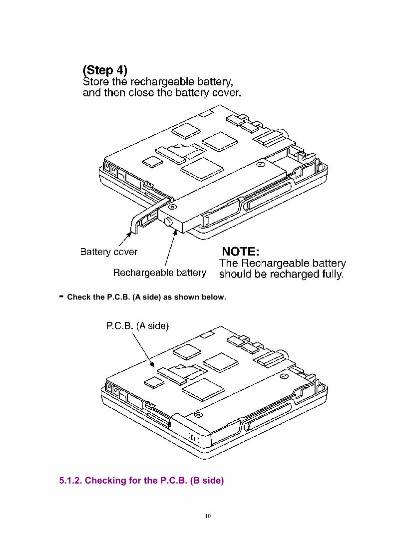
- Check the P.C.B. (A side) as shown below.
5.1.2. Checking for the P.C.B. (B side)
10

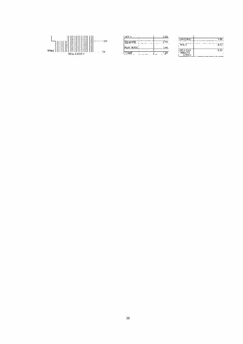
- To check the IC501 on side B of P.C.B., refer to the table 1 and illustration below.
11

12
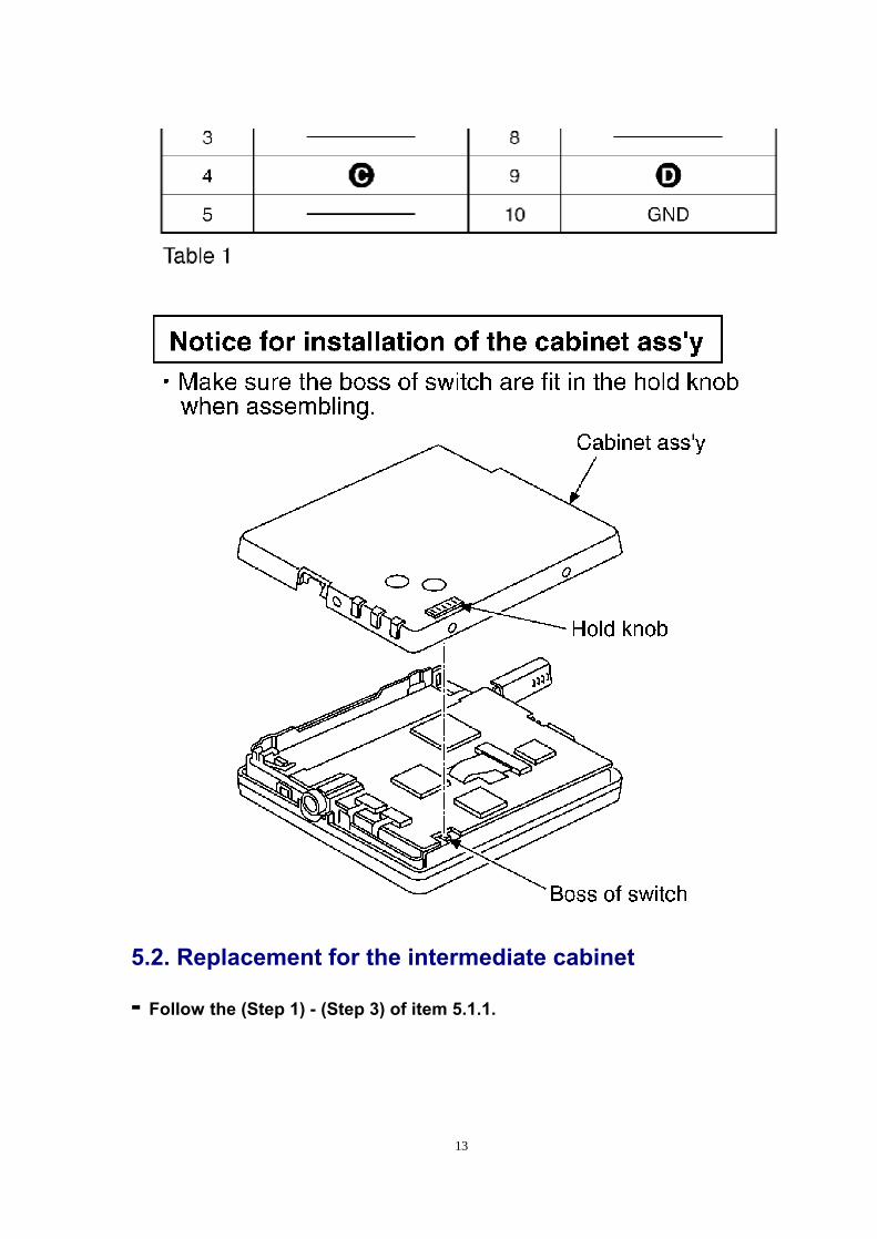
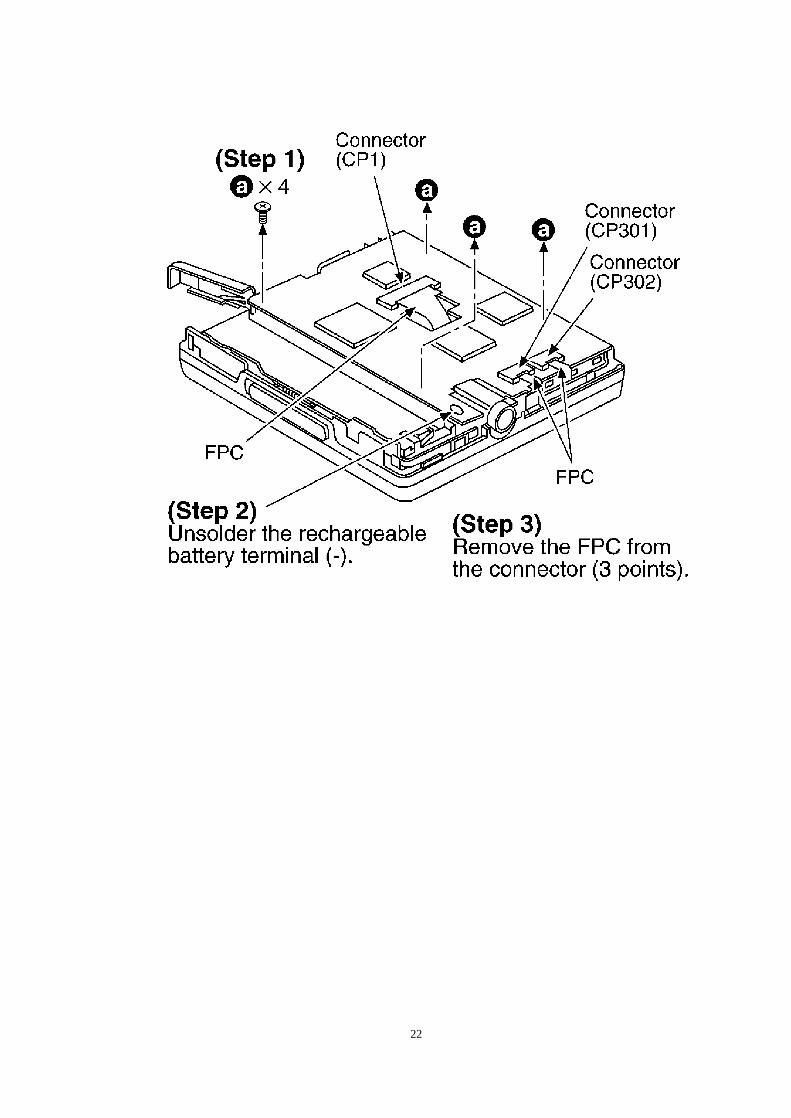
5.2. Replacement for the intermediate cabinet
- Follow the (Step 1) - (Step 3) of item 5.1.1.
13

14

15

16

17

18

5.3. Replacement for the disc cover ass'y
- Follow the (Step 1) - (Step 3) of item 5.1.1.
- Follow the (Step 1) - (Step 4) of item 5.2.
19

20

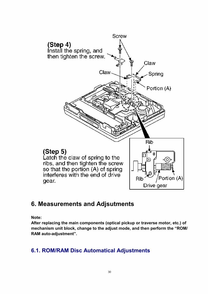
5.4. Replacement for the traverse motor
- Follow the (Step 1) - (Step 3) of item 5.1.1.
21
22

23

24

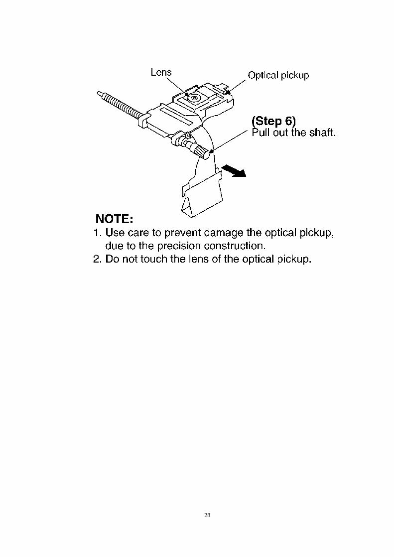
5.5. Replacement for the optical pickup
- Follow the (Step 1) - (Step 3) of item 5.1.1.
- Follow the (Step 1) - (Step 5) of item 5.4.
25

26

27
28

29
6. Measurements and Adjsutments
Note:After replacing the main components (optical pickup or traverse motor, etc.) of mechanism unit block, change to the adjust mode, and then perform the “ROM/RAM auto-adjustment”.
6.1. ROM/RAM Disc Automatical Adjustments
30

6.1.1. Necessary instruments to adjust
1. Test disc (Playback-only disc)2. Commercially available recordable disc (fully recorded with music) (magneto-
optical disc)3. Remote controller
6.1.2. Preparations for adjustment
1. Check the laser emission.A. Make the player to the mechanism unit only. (Refer to Fig.3 or the item of
“Replacement for the intermediate cabinet” in “Operation Checks and Main Component Replacement Procedures).
B. Set the battery.C. While pressing the battery cover to connect the battery power,
continuously press the OPEN/CLOSE switch. (As shown in Fig.4)D. The optical pickup moves up and down and emits a laser. (Caution: Do not
look directly at the laser light source.) If the laser does not emit a beam, follow the item of “operation check” in “Troubleshooting Guide ” and check for a malfunction.
E. Make the optical pickup move to the center of the movement range (refer to Fig.4) (Note : Do not touch the optical pick up lens.).
F. Remove the battery.
Fig.4
31

6.1.3. Enter the adjustment mode
1. Mount the mechanism unit on the disc cover. (Shown in the item of “Replacement for the intermediate cabinet” in “Operation Checks and Main Component Replacement Procedures”).
2. Connect the remote controller, set the battery and close the battery cover.3. Turn off the power, select for OFF the main unit’s HOLD switch.4. Press the remote controller’s keys in between two seconds, enter the
adjustment mode.A. Press VOL+ button by your right thumb, and press VOL-button by your left
thumb with keeping on pressing VOL+ button.B. Release VOL+ button with keeping on pressing VOL-button, and press
button by your right thumb.C. Release VOL-button with keeping on pressing button, and press
button by your left thumb.Release button with keeping on button, and release button.(a-c are shown in Fig.5)
Fig.5
32

5. When the adjustment mode is activated, “TE” will be displayed. After “TE” is displayed, select the desired adjustment item with the button or button.
Adjustment modeAdjustment mode Display
Playback-only disc automatic adjustment
T1
Magneto-optical disc automatic adjustment
T2
Playback-only disc automatic adjustment value check
T3
Magneto-optical disc automatic adjustment value check
T4
Laser power check T5EFM jitter measurement T6ADIP jitter measurement T7Error rate measurement T8Tilt measurement T9PWB inspection (audio test) TAEEPROM check TE
*In the display of T1 ~ TE shown above, you must adjust T1 and T2.
6.1.4. Playback-only disc automatic adjustment
With the T1 displayed, set the test disc and press the PLAY key to active the adjustment mode.During the adjustment, “OADJ” will be displayed. If there are no abnormalities, “OOK” will be displayed. (Note1)If the key is pressed while the “OOK” or “ONG” is being displayed, the setting returns to the T1 display.When finished, remove the disc.
33

Note 1:When “ONG” is displayed, follow the item of “operation check” in “Troubleshooting Guide” and check for a malfunction.
6.1.5. Magneto-optical disc automatic adjustment
With the T2 displayed, set the commercially available recordable disc (which is fully recorded with music).Press key to activate the adjustment mode.During the adjsutment, “AADJ” will be displayed. If there are no abnormalities, “AOK” will be displayed. (Note 2)If key is pressed while the “OOK” or “ONG” is being displayed, the setting returns to the T2 display.When finished, remove the disc.
Note 2:When “ANG” is displayed, follow the item of “operation check” in “Troubleshooting Guide” and check for a malfunction.
*To exit the adjustment mode, remove the battery.
6.2. Checking the main unit's keys
1. Set the battery and connect the remote controller.2. Turn off the power, select for OFF the main unit’s HOLD switch.3. Press the remote controller’s keys in between two seconds, enter the
adjustment mode.A. Press VOL+ button by your right thumb, and press VOL-button by your left
thumb with keeping on pressing VOL+ button.B. Release VOL+ button with keeping on pressing VOL-button, and press
button by your right thumb.C. Release VOL-button with keeping on pressing button, and press
button by your left thumb.Release button with keeping on button, and release button.(a-c are shown in Fig.6)
Fig.6
34

4. When entering the main unit’s key check mode, “KEY JP” will be displayed.When “KEY JP” is displayed, press , , , VOL (+/-) keys and set the HOLD switch to OFF (no order). Then, “KEY OK” will be displayed.
Note:If “KEY OK” is not displayed, check the following voltage for each key.
Key Test point ON OFFIC201-35 pin 0V 2.3V
HOLD TPX110 2.3V 0VVOL + TP307 0V 2.3VVOL - TP307 0.6V 2.3V
TP307 1.2V 2.3VTP307 1.7V 2.3V
To exit the main unit’s key check mode, remove the battery.
Note:Refer to “Printed Circuit Board and Wiring Connection Diagram” for the test points.
7. Troubleshooting Guide
35

36

37
38

39

40

41

42

43

44

8. Schematic Diagram Notes
8.1. Schemtic Diagram NotesThis schematic diagram may be modified at any time with the development of new technology.
Notes:
- S201 : Volume (VOLUME +) switch.
- S202 : Volume (VOLUME -) switch.
- S203 : F. skip / search ( ) switch.
- S204 : R. skip / search ( ) switch.
- S206 : Play / stop ( ) switch.
- S207 : Cover open / close det. switch.
- S208 : Hold switch in “OFF” position.
- Indicated voltage values are the standard values for the unit measured by the DC electronic circuit tester (high-impedance) with the chassis taken as standard. Therefore, there may exist some errors in the voltage values, depending on the internal impedance of the DC circuit tester.
No mark: MD STOP ( ): MD play [1kHz, L+R, 0dB]
Important safety notice:Components identified by mark have special characteristics important for safety.Furthermore, special parts which have purpose of fire-retardant (resistors), high-quality sound (capacitors), low-noise (resistors), etc. are used. When replacing any of components, be sure to use only manufacture's specified parts shown in the parts list.
Caution!IC and LSI are sensitive to static electricity.Secondary trouble can be prevented by taking care during repair.Cover the parts boxes made of plastics with aluminum foil.Ground the soldering iron.Put a conductive mat on the work table.
45

Do not touch the legs of IC or LSI with the fingers directly.
Voltage and signal line
: Positive voltage line
: Playback signal line
8.2. Type Illustration of IC's, Transistors and Diodes
9. Schematic Diagram
10. Printed Circuit Board and Wiring Connection Diagram
11. Block Diagram
12. Terminal Function of IC 's
12.1. IC1 (LA9607T-TFM) : RF AMP
46

Pin No.
Mark I/O Division
Function
1 PPIT — Pit/Group discrimination input terminal (“H”:pit, “L”:group) (Not used, open)
2 VCC I Power supply input terminal
3 J I RF signal that I-V converted input terminal4 I
5 F I Side beam signal that I-V converted input terminal6 E
7 D I Main beam signal that I-V converted input termianl8 C
9 B10 A11 VEE — GND terminal12 LDO O APC output terminal13 LDS I Laser light quantity that I-V
converted input terminal14 LDREF I Laser control signal input
terminal15 FBAL I Focus balance control
signal input terminal16 TBAL I Tracking balance control
signal input terminal17 TOFFSET I Tracking offset control
signal input terminal18 FOFFSET I Tracking offset control
signal input terminal19 AOFFSET I ABCD offset control signal
input terminal20 SGC I AGC control signal input
terminal21 DSW0 I Disc mode setting input
terminal (“H”:low reflection rate disc, “L”:high reflection rate disc, both DSW0 and DSW1 are “L”:laser off)
22 DSW1 I Disc mode setting input terminal (“H”:track is pit-row, “L”:track is group, both DSWO and DSW1 are “L”:laser off)
47

Pin No.
Mark I/O Division
Function
23 VR I For pass-com 1/2 VCC (reference voltage) input terminal
24 VC O 1/2 VCC (reference voltage) output terminal
25 FE O Focus error signal output terminal
26 TE O Tracking error signal output terminal
27 ABCD O Main beam light quantity signal output terminal
28 HFLI I For making HFL signal input terminal (when group mode)
29 BOTTOM O Bottom signal of RF signal output terminal
30 PEAK O Peak signal of RF signal output terminal
31 HFL O Track detection signal input terminal
32 BHC — Connected to GND through capacitor33 PHC
34 RFVEE — GND terminal35 EQ0 O RF equalizer output
terminal36 EQI I RF equalizer input terminal37 RFO O RF signal output terminal38 RFVCC I Power supply input
terminal39 ADIPCR O ADIP carrier signal output
terminal40 3TSW I 3T/11T monitor terminal
select switch input terminal41 GLHSW — GND terminal42 RAGCSW I RF AGC ON/OFF select
switch input terminal43 WDO O Wobble signal output
terminal44 WOI I Wobble signal input
terminal45 SETR I Band pass filter set ting
input terminal
48

Pin No.
Mark I/O Division
Function
46 CAD I Capaciter for DC cut of Wobble signal connect terminal
47 BWCT I Band pass filter select terminal for wobble signal
48 SLEEP I Sleep mode terminal (“H”:power supply ON, “L”:power supply OFF) (Connected to power supply through capacitor)
12.2. IC101 (LC89642-8A) : MSP
Pin No.
Mark I/O Division
Function
1 FR I Bias resistor terminal of VCEC oscillation frequency (Connected to power supply through resistor)
2 ISET I Bias resistor terminal of VCEC voltage charge pump (Connected to power supply through resistor)
3 VCVDD I Power supply terminal for VCEC
4 PDO O VCEC voltage charge pump output terminal (Connected to GND through resistor and capacitor)
5 TEST3 I Intput terminal for test(Connected to power supply)
6 TEST2 I Input terminal for test(Connected to power supply)
7 SLCO O Slice level of HF signal output terminal
8 SLCIST I Slice level adjustment amp. bias resistor terminal
9 EFMIN I RF equalizer input terminal10 RESETB I System reset B signal
input terminal
49

Pin No.
Mark I/O Division
Function
11 TEST1 I Input terminal for test (Connected to power supply)
12 HFL I Track detection signal input terminal
13 VDD2 I Power supply terminal14 VSS — GND terminal15 VDD1 I Power supply terminal16 AVSS1 — GND terminal17 PEAK I Peak signal of RF input
terminal18 BOTTOM I Bottom signal of RF input
terminal19 ABCD I Main beam light quantity
signal input terminal20 TE I Tracking error signal input
terminal21 FE I Focus error signal input
terminal22 VC I 1/2 VCC
(reference voltage input terminal)
23 AVDD1 I Power supply terminal24 MAD9 O Adress output terminal to
DRAM(Not used, open)
25 DSW1 O Disc mode setting output terminal (“H”:track is pit-low, “L”:high reflection rate disc)
26 MAD8 O Adress output terminal to DRAM(Not used, open)
27 DSW0 O Disc mode setting output terminal (“H”:low reflection rate disc, “L”:high reflection rate disc)
28 MAD7 O Adress output terminal to DRAM(Not used, open)
29 SGC O AGC control signal output terminal
50

Pin No.
Mark I/O Division
Function
30 MAD6 O Adress output terminal to DRAM(Not used, open)
31 AOFF SET
O ABCD offset control signal output terminal
32 MAD5 O Adress output terminal to DRAM(Not used, open)
33 FOFF SET
O Focus offset control signal output terminal
34 TOFF SET
O Tracking offset control signal output terminal
35 MAD4 O Adress output terminal to DRAM(Not used, open)
36 TBAL O Tracking balance control signal output terminal
37 LDREF O Laser control signal output terminal
38 FBAL O Focus balance control signal output terminal
39 VDD1 I Power supply terminal40 VSS — GND terminal41 VDD2 I Power supply terminal42 MAD3 O Adress output terminal to
DRAM(Not used, open)
43 SPP WMF
O Spindle PWM output terminal
44 SPP WMR
45 SLP WMF
O Sled PWM output terminal
46 MAD2 O Adress output terminal to DRAM(Not used, open)
47 SLP WMR
O Sled PWM output terminal
48 MAD1 O Adress output terminal to DRAM(Not used, open)
49 FOP WMF
O Focus PWM output terminal
51

Pin No.
Mark I/O Division
Function
50 MAD0 O Adress output terminal to DRAM(Not used, open)
51 FOP WMR
O Focus PWM output terminal
52 TRP WMF
O Tracking PWM output terminal
53 TRP WMR
54 TESTI0 — Input terminal for test(Not used, open)
55 AVDD I Power supply terminal56 OUTL O 1 bit DAC L channel output
terminal57 OUTR O 1 bit DAC R channel output
terminal58 AVSS — GND terminal59 VDD2 I Power supply terminal60 X IN I Crystal oscillator input
teminal (f=16.9344MHz)61 X OUT O Crystal oscillator output
teminal (f=16.9344MHz)62 VSS — GND terminal63 VDD1 I Powe supply terminal64 F16M O 16.9344MHz output terminal
(Not used, open)65 ENH O De-emphasis output
terminal(Not used, open)
66 LRCO O LR clock output terminal(Not used, open)
67 DDATA O Not used, open68 BCO O Bit clock output terminal
(Not used, open)69 DDOUT O Digital audio output
terminal(Not used, open)
70 SMON3 O Monitor signal output terminal(Not used, open)
71 SMON2 O Monitor signal 2 output terminal
72 SMON1 O Monitor signal 1 output terminal
52

terminalPin No.
Mark I/O Division
Function
73 SMON0 O Monitor signal 0 output terminal(Not used, open)
74 FSEQ O Flame detection signal output terminal (Not used, open)
75 VP O CLV servo clock judgement signal output terminal (Not used, open)
76 MCST — Not used, open77 MRASB O RAS signal to DRAM
output terminal (Not used, open)
78 FOK O Focus OK signal output terminal
79 MWEB — Not used, open80 DEFECT O Defect signal output
terminal(Not used, open)
81 MD1 I/O Data in/output terminal to DRAM(Not used, open)
82 FG I Speed pulse input terminal83 CL I CPU interface data clock
input terminal84 CE I CPU interface chip enable
signal input terminal85 MD0 I/O Data in/output terminal to
DRAM(Not used, open)
86 DI I CPU interface data clock input terminal
87 VDD1 I Power supply terminal88 DO O CPU interface data output
terminal89 VDD2 I Power supply terminal90 VSS — GND terminal91 MD3 I/O Data in/output terminal to
DRAM92 WRQB O CPU interface interrupt
signal output terminal93 INTB O CPU interface interrupt
signal output terminal
53

Pin No.
Mark I/O Division
Function
94 ADIPWO I Wobble signal input terminal
95 MD2 I/O Data in/output terminal to DRAM
96 SHOCK O Shock detection signal output terminal
97 MCASB O CAS signal to DRAM output terminal(Not used, open)
98 PCK O VCEC clock signal output terminal(Not used, open)
99 MOEB O OE signal to DRAM output terminal(Not used, open)
100 VCVSS — GND terminal
12.3. IC201 (MN101C28DAD1) : SYSTEM CONTROL
Pin No.
Mark I/O Division
Function
1 VREF- — Reference voltage- input terminal (Connected to GND)
2 AN0 — Not used, connected to GND through resistor
3 BATT I Battery voltage detect terminal
4 KEY IN I Key input terminal5 AN3 I Area select termianl
(Connected to power supply through resistor)
6 REM KEY
I Remocon key input terminal
7 DOCTOR I Check mode input terminal (“L”:check mode)(Connected to power supply through resistor)
8 AN6 — Not used, connected to GND
9 SE I Sled error voltage input terminal
54

Pin No.
Mark I/O Division
Function
10 VREF+ I Reference voltage+ input terminal
11 VDD I Power supply terminal12 OSC2 I System clock input
terminal (6MHz)13 OSC1 O System clock output
terminal (6MHz)14 VSS — GND terminal15 XI I Sub clock input terminal
(Not used, connected to GND)
16 XO O Sub clock output terminal (Not used, open)
17 MMOD — Memory mode select terminal (Connected to GND)
18 REM DATA
O LCD driver data output terminal
19 LINK IN I Link serial communication clock signal input terminal
20 — — Not used, open21 SSDW O CPU interface data output
terminal22 SSDR I CPU interface data input
terminal23 SSCLK O CPU interface data clock
output terminal24 BUZZER O Buzzer control output
terminal25 RST I Reset signal input terminal 26 SELAD O CPU interface chip enable
output terminal27 — — Not used, open28 SE TR O Band pass filter set
terminal29 — — Not used, open30 BWCT O Band pass filter select
output terminal31 INTB I CPU interface interrupt
input terminal32 WRQB33 REM
WUPI Remocon wake up
interrupt input terminal
55

Pin No.
Mark I/O Division
Function
34 OPEN SW
I Cover open/close detect terminal (“H”:open)
35 PLAY KEY
I Play key input terminal (“L”:STOP/PLAY)
36 AGC TC O RF AGC select output terminal (Not used, open)
37 PC O Driver IC stand by output terminal
38 ZDTCL I Lch no signal detect input terminal (“H”:no signal)
39 FOK I Focus OK signal input terminal
40 ZDTCR I Rch no signal detect input terminal (“H”:no signal)
41 RESETB O System reset output terminal
42 — — Not used, open4344 UO O Stepping motor control
output terminal45 VO46 WO47 UI I Stepping motor control
input terminal48 VI49 WI50 LDON O Laser on output terminal
(“L”:laser ON)51 — — Not used, open52 EEPDATA0 O EEP ROM data output
terminal53 EEPCK O EEP ROM clock output
terminal54 EEPCS O EEP ROM chip select
output terminal55 EEPDATAI I EEP ROM data input
terminal56 — — Not used, open57 HOLD I Hold switch input terminal
(“L”:Hold switch off)58 MUTEA O Analog mute A output
terminal59 MUTEB O Analog mute B output
terminal60 — — Not used, open
56

Pin No.
Mark I/O Division
Function
61 STBY2 O 4ch driver IC stand by 2 output terminal
62 RFCONT O RF amp power control output terminal
63 SEDIR I Sled error direction input terminal
64 TBALOK O Tracking balance adjustment output terminal (“H”:adjustment)(Not used, open)
65~ 68
— — Not used, open
69 3TSW O 3T/11T monitor select switch output terminal
70 RAGCSW O RF AGC ON/OFF select switch output terminal
71 SHOCK I Shock det. input terminal72~ 78
— — Not used, open
79 ELON O EL display control output terminal (“L”:EL on)
80 P.CONT O Power control output terminal
12.4. IC301 (BD6605KVT) : FOCUS/TRACKING COIL, TRAVERSE MOTOR DRIVE, SPINDLE MOTOR DRIVE, ROTARY DETECTOR
57

Pin No.
Mark I/O Division
Function
1 SPWIN I Roter position detect comparater(W) input terminal
2 SPCOM I Spindle motor coil center input terminal
3 EXTCLK I Not used, open4 C1P — Charge pump capacitor 1(+)
connect terminal5 C1M — Charge pump capacitor 1(-)
connect terminal6 C2P — Charge pump capacitor 2(+)
connect terminal7 C2M — Charge pump capacitor 2(-)
connect terminal8 VG O Charge pump output
terminal9 SLVM1 I Power supply terminal10 SLUOUT O Stepping motor (U) output
terminal11 SLPG1 — GND terminal12 SLVOUT O Stepping motor (V) output
terminal13 SLVM2 I Power supply terminal14 SLWOUT O Stepping motor (W) output
terminal15 SLPG2 — GND terminal16 SLCOM I Step motor coil center
input terminal17 BEMFW O Step detect comparater(W)
output terminal18 BEMFV O Step detect comparater(V)
output terminal19 BEMFU O Step detect comparater(U)
output terminal20 S3 I Stepping decorder 3 input
terminal21 S2 I Stepping decorder 2 input
terminal22 S1 I Stepping decorder 1 input
terminal23 SGND — GND terminal24 ASGND — GND terminal
58

Pin No.
Mark I/O Division
Function
25 STHB I H1, H2 bridge mute input terminal
26 STALL I Standby input terminal27 PW1VM I Power supply terminal28 PW1OUT O Half bridge 1 output
terminal(Not used, open)
29 PWPG — GND terminal30 PW2OUT O Half bridge 2 output
terminal31 PW2VM I Power supply terminal32 PWIN2 I Half bridge input terminal33 PWIN1 — GND terminal34 IN 2R I H bridge 2 reverse input
terminal35 IN 2F I H bridge 2 forward input
terminal36 IN 1R I H bridge 1 reverse input
terminal37 IN 1F I H bridge 1 forward input
terminal38 H2 PG2 — GND terminal39 H2 R
OUTO H bridge 2 reverse output
terminal40 H2 VM I Power supply terminal41 H2 F
OUTO H bridge 2 forward output
terminal42 H2PG1 — GND terminal43 H1 PG2 — GND terminal44 H1 R
OUTO H bridge 1 reverse output
terminal45 H1 VM I Power supply terminal46 H1 F
OUTO H bridge 1 forward output
terminal47 H1 PG1 — GND terminal48 CST — Connected to GND through
capaciter49 CSL1 I Slope capacitor connection
terminal (Connected to GND through capacitor)
50 CSL2
51 FG O Speed pulse output terminal
59
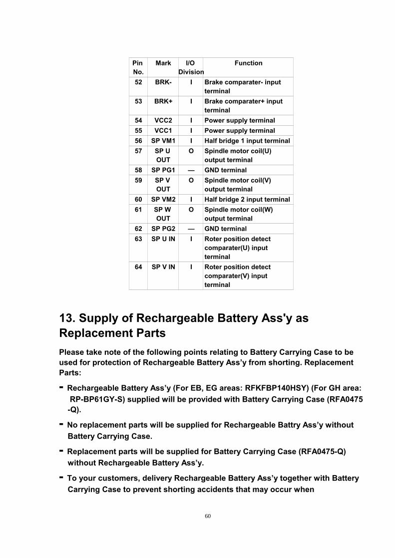
Pin No.
Mark I/O Division
Function
52 BRK- I Brake comparater- input terminal
53 BRK+ I Brake comparater+ input terminal
54 VCC2 I Power supply terminal55 VCC1 I Power supply terminal56 SP VM1 I Half bridge 1 input terminal57 SP U
OUTO Spindle motor coil(U)
output terminal58 SP PG1 — GND terminal59 SP V
OUTO Spindle motor coil(V)
output terminal60 SP VM2 I Half bridge 2 input terminal61 SP W
OUTO Spindle motor coil(W)
output terminal62 SP PG2 — GND terminal63 SP U IN I Roter position detect
comparater(U) input terminal
64 SP V IN I Roter position detect comparater(V) input terminal
13. Supply of Rechargeable Battery Ass'y as Replacement PartsPlease take note of the following points relating to Battery Carrying Case to be used for protection of Rechargeable Battery Ass’y from shorting. Replacement Parts:
- Rechargeable Battery Ass’y (For EB, EG areas: RFKFBP140HSY) (For GH area: RP-BP61GY-S) supplied will be provided with Battery Carrying Case (RFA0475-Q).
- No replacement parts will be supplied for Rechargeable Battry Ass’y without Battery Carrying Case.
- Replacement parts will be supplied for Battery Carrying Case (RFA0475-Q) without Rechargeable Battery Ass’y.
- To your customers, delivery Rechargeable Battery Ass’y together with Battery Carrying Case to prevent shorting accidents that may occur when
60

Rechargeable Battery Ass’y is carried about Battery Carrying Case. (as shown in Fig.6)
Fig.7
14. Caution in Use of Rechargeable Battery Ass'y
- Take Rechargeable Battery Ass’y out of Battery Carrying Case and use it.
- Be sure to carry Rechargeable Battery Carrying Case. If not, it may either heat or ignite by shorting with a metal. (as shown in Fig.8)
Fig.8
61

15. Replacement Parts List
15.1. Replacement Parts List
Notes:*Important safety notice:Components identified by mark have special characteristics important for safety.Funrthermore, special parts which have purposes of fire-retardant (resistors), high-quality sound (capacitors), low-noise (resistors), etc. are used.When replacing any of components, be sure to use only manufacture’s specified parts shown in the parts list.*Warning: This product uses a laser diode. Refer to caution statements.*ACHTUNG:Die lasereinheit nicht zerlegen.Die lasereinheit darf nur gegen einc vom hersteller spezifizierte einheit ausgetauscht werden.*Capacity values are in microfarads (uF) unless specified otherwise, P=Pico-farads (pF) F=Farads (F)*Resistance values are in ohms, unless specified otherwise, 1K=1,000 (OHM), 1M=1,000K (OHM)*The marking <RTL> indicates that the Retention Time is limited for this item. After the discontinuation of this assembly in production, the item will continue to be available for a specific period of time. The retention period of availability is dependant on the type of assembly , and in accordance with the laws governing part and product retention. After the end of this period, the assembly will no longer be available.*"<IA>" mark in Remarks indicate languages of instruction manual.[<IA> : English/ Spanish/ French/ German/ Netherlands/ Swedish/ Italian/ Russian/ Polish/ Danish/ Czeco, <IB> : English/ Chinese]
62

Ref. No. Part No. Part Name & Description Pcs Remarks
1 RHQ0083-S SCREW 42 RXQ0658-3 LINK UNIT(L) 13 RXQ0659-1 LINK UNIT(R) 14 RXQ0660 HOLDER ASS'Y 15 RYF0531Z-S DISC COVER ASS'Y 16 RYQ0273-S INTERMEDIATE CABINET 16-1 RGV0255-S OPEN KNOB 17 RYK0977A-S CABINET ASS'Y 1 (EB)(EG)7 RYK0977B-S CABINET ASS'Y 1 (GH)7-1 RGK1210-S JACK PIECE 17-2 RGU1817-S BUTTON,OPERATION 17-3 RGU1818-S BUTTON,VOLUME 17-4 RGV0256-S HOLD KNOB 18 RHD14076-S SCREW 69 RKK0133-S BATTERY COVER 110 RAE1611Z MECHANISM UNIT 110-1 RDG0446 INTERMEDIATE GEAR 110-2 RHD14067 SCREW 110-3 RHW11011 WASHER 110-4 RMC0392-1 SPRING 110-5 RXJ0025 SHAFT 110-6 RXK0293 TRAVERSE UNIT 110-6A BQL1A1CWD2 TRAVERSE MOTOR 110-6B RHD14074 SCREW 110-6C RJC99038 R.BATT.TERMINAL(-) 110-6D RMX0156 STOPPER RUBBER 110-6E XQN14+B2FC SCREW 110-7 RAF1620A OPTICAL PICKUP 110-8 RHD14005 SCREW 110-9 RMC0371-1 SPRING 111 RHD14067 SCREW 512 RJC99039 R.BATT.TERMINAL(+) 113 RJR0195 BATTERY SHAFT 1
A1 RFKFBP140HSY RECHARGEABLE BATT.ASS'Y 1 (EB)(EG)A1 RP-BP61GY-S RECHARGEABLE BATT.ASS'Y 1 (GH)A1-1 RFA0475-Q RECHARGEABLE BATT.CASE 1A2 RFA1136-H BATTERY CASE 1A3 RFC0056-K CARRING CASE 1A4 RFEV025P-SM REMOTE CONTROL 1A5 RFEV319P-S1A STEREO INSIDEPHONES 1A6 RP-BC155AEBY CHARGER 1 (EB)A6 RP-BC155AEYB CHARGER 1 (EG)A6 RP-BC155AGH CHARGER 1 (GH)A7 RQA0117 WARRANTY CARD 1 (EB)(EG)A8 RQCB0169 SERVICENTER LIST 1A9 RQT5331-B INSTRUCTION MANUAL 1 (EB)(EG)<IA>A9 RQT5332-G INSTRUCTION MANUAL 1 (GH)<IB>
C1 ECUVNJ105KBV 63V 1U 1
63

Ref. No. Part No. Part Name & Description Pcs RemarksC2 ECUE1C103KBQ 16V 0.01U 1C4 ECUE1H120JCQ 50V 12P 1C5 ECUVNJ105KBV 63V 1U 1C6 ECUVNA224KBV 10V 0.22U 1C7 ECUE1H040CCQ 50V 4P 1C8 ECUVNJ105KBV 63V 1U 1C10 ECUENA104KBQ 10V 0.1U 1C11 RCST0GZ226RG 4V 22U 1C12 ECUENA104KBQ 10V 0.1U 1C13 RCST0GZ106RG 4V 10U 1C14 ECUENA104KBQ 10V 0.1U 1C17,18 ECUV1C823KBV 16V 0.082U 2C19 ECUENA104KBQ 10V 0.1U 1C20 ECUE1H332KBQ 50V 3300P 1C21 ECUE1C103KBQ 16V 0.01U 1C23 ECUE1H332KBQ 50V 3300P 1C24 ECUENA104KBQ 10V 0.1U 1C25 RCST0GZ106RG 4V 10U 1C27-29 ECUE1H102KBQ 50V 1000P 3C101 RCST0EX227RE 2.5V 220U 1C102 ECUENA104KBQ 10V 0.1U 1C103 ECUENA473KBQ 10V 0.047U 1C110,11 ECUENA104KBQ 10V 0.1U 2C113,14 ECUENA104KBQ 10V 0.1U 2C115 ECUE1C103KBQ 16V 0.01U 1C119-23 ECUENA104KBQ 10V 0.1U 5C124,25 ECUE1C103KBQ 16V 0.01U 2C127 ECUE1C223KBQ 16V 0.022U 1C128 ECUENA104KBQ 10V 0.1U 1C129 ECUENC333KBQ 16V 0.033U 1C138 ECUENA104KBQ 10V 0.1U 1C201 ECUE1C103KBQ 16V 0.01U 1C202 ECUE1H101KBQ 50V 100P 1C203 RCST0GZ106RG 4V 10U 1C204 ECUENA104KBQ 10V 0.1U 1C206 ECUE1H101KBQ 50V 100P 1C210 ECUE1C103KBQ 16V 0.01U 1C211 ECUV0J474KBV 6.3V 0.47U 1C212 ECUE1C103KBQ 16V 0.01U 1C220,21 ECUVNA224KBV 10V 0.22U 2C301,02 ECUE1H221KBQ 50V 220P 2C303 RCST0GZ226RG 4V 22U 1C304-06 ECUENA104KBQ 10V 0.1U 3C307 RCST0GZ106RG 4V 10U 1C308 ECUENA104KBQ 10V 0.1U 1C309-11 ECUENC333KBQ 16V 0.033U 3C318 ECUVNA224KBV 10V 0.22U 1C319,20 ECUENC333KBQ 16V 0.033U 2C323-25 ECUE1H222KBQ 50V 2200P 3C330-33 ECUVNJ105KBV 63V 1U 4C401 EEVMC0G221P 4V 220U 1C404 EEFCD0J470R 6.3V 47U 1C406,07 RCST0GZ106RG 4V 10U 2C408 RCST0GZ226RG 4V 22U 1
64
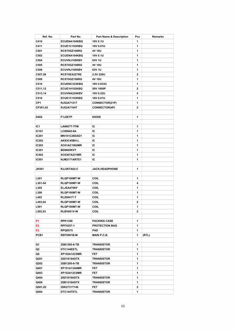
Ref. No. Part No. Part Name & Description Pcs RemarksC410 ECUENA104KBQ 10V 0.1U 1C411 ECUE1C103KBQ 16V 0.01U 1C501 RCST0GZ106RG 4V 10U 1C502 ECUENA104KBQ 10V 0.1U 1C504 ECUVNJ105KBV 63V 1U 1C505 RCST0GZ106RG 4V 10U 1C506 ECUVNJ105KBV 63V 1U 1C507,08 RCST0EX227RE 2.5V 220U 2C509 RCST0GZ106RG 4V 10U 1C510 ECUENC333KBQ 16V 0.033U 1C511,12 ECUE1H102KBQ 50V 1000P 2C513,14 ECUVNA224KBV 10V 0.22U 2C516 ECUE1C103KBQ 16V 0.01U 1CP1 RJS2A7121T CONNECTOR(21P) 1CP301,02 RJS2A7104T CONNECTOR(4P) 2
D402 F1J2ETP DIODE 1
IC1 LA9607T-TFM IC 1IC101 LC89642-8A IC 1IC201 MN101C28DAD1 IC 1IC202 AK93C45BH-L IC 1IC203 XC61AC1902MR IC 1IC301 BD6605KVT IC 1IC402 XC6367A231MR IC 1IC501 NJM2171ARTE1 IC 1
JK501 RJJ36TA02-C JACK,HEADPHONE 1
L201 RLQP100MT-W COIL 1L301-04 RLQP100MT-W COIL 4L305 ELJEA470KF COIL 1L306 RLQP100MT-W COIL 1L402 RLZ0041T-T COIL 1L403,04 RLQP100MT-W COIL 2L501 RLQP100MT-W COIL 1L502,03 RLBV601V-W COIL 2
P1 RPK1348 PACKING CASE 1P2 RPF0257-1 PROTECTION BAG 1P3 RPQ0575 PAD 1PCB1 REP2901B-M MAIN P.C.B. 1 (RTL)
Q1 2SB1295-6-TB TRANSISTOR 1Q2 DTC144EETL TRANSISTOR 1Q5 XP152A12C0MR FET 1Q201 2SD1819ASTX TRANSISTOR 1Q202 2SB1295-6-TB TRANSISTOR 1Q401 XP151A13A0MR FET 1Q403 XP152A12C0MR FET 1Q404 2SD1819ASTX TRANSISTOR 1Q406 2SB1218ASTX TRANSISTOR 1Q501,02 2SK2731T146 FET 2Q504 DTC144TETL TRANSISTOR 1
65

Ref. No. Part No. Part Name & Description Pcs Remarks
R1 ERJ2GEJ821X 1/4W 820 1R2 ERJ2GEJ104X 1/4W 100K 1R3 EXB24V113JX 1/16W 11K 1R4 ERJ2GEJ391X 1/4W 390 1R6 ERJ2GEJ823X 1/4W 82K 1R7 ERJ2GEJ223X 1/4W 22K 1R8 ERJ2GEJ474X 1/4W 470K 1R9 ERJ2GEJ105X 1/4W 1M 1R20,21 ERJ2GEJ104X 1/4W 100K 2R24 ERJ2GEJ393X 1/4W 39K 1R40 ERJ2GEJ1R0X 1/4W 1 1R101 ERJ2GED683X 1/4W 68K 1R102 ERJ2GEJ103X 1/4W 10K 1R103 ERJ2GEJ334X 1/4W 330K 1R104 ERJ2GEJ564X 1/4W 560K 1R105 ERJ2GEJ683X 1/4W 68K 1R106 ERJ2GED113X 1/4W 11K 1R107 ERJ2GEJ103X 1/4W 10K 1R108 ERJ2GEJ104X 1/4W 100K 1R109 ERJ2GEJ473X 1/4W 47K 1R113 ERJ2GEJ473X 1/4W 47K 1R114 ERJ2GEJ474X 1/4W 470K 1R122 ERJ2GEJ470X 1/4W 47 1R125 ERJ2GEJ332X 1/4W 3.3K 1R126 ERJ2GEJ682X 1/4W 6.8K 1R127 ERJ2GEJ333X 1/4W 33K 1R128 ERJ2GEJ391X 1/4W 390 1R130 ERJ2GEJ562X 1/4W 5.6K 1R131 ERJ2GEJ332X 1/4W 3.3K 1R201 EXB24V103JX 1/16W 10K 1R202 ERJ2GEJ332X 1/4W 3.3K 1R203 ERJ2GEJ221X 1/4W 220 1R204 ERJ2GEJ332X 1/4W 3.3K 1R205 ERJ2GEJ682X 1/4W 6.8K 1R206 ERJ2GEJ223X 1/4W 22K 1R207 ERJ2GEJ471X 1/4W 470 1R208 EXB28V224JX 1/32W 220K 1R210 ERJ2GEJ224X 1/4W 220K 1R214 ERJ2GEJ334X 1/4W 330K 1R218 ERJ2GED273X 1/4W 27K 1R219 EXB28V103JX 1/32W 10K 1R225 ERJ2GEJ223X 1/4W 22K 1R230 EXB24V103JX 1/16W 10K 1R231 ERJ2GEJ104X 1/4W 100K 1R301 ERJ2GEJ103X 1/4W 10K 1R302 ERJ2GEJ105X 1/4W 1M 1R303 ERJ2GEJ103X 1/4W 10K 1R304 ERJ2GEJ1R0X 1/4W 1 1R313 EXB24V473JX 1/16W 47K 1R401 ERJ2GEJ225X 1/4W 2.2M 1R404 ERJ2GEJ274X 1/4W 270K 1R405 ERJ2GEJ105X 1/4W 1M 1R501 EXB24V472JX 1/16W 4.7K 1
66

Ref. No. Part No. Part Name & Description Pcs RemarksR504 EXB24V153JX 1/16W 15K 1R505 EXB24V821JX 1/16W 820 1R506 EXB24V225JX 1/16W 2.2M 1R507,08 EXB24V472JX 1/16W 4.7K 2R509 ERJ2GEJ270X 1/4W 27 1R510,11 ERJ2GEJ104X 1/4W 100K 2RX229 ERJ2GEJ104X 1/4W 100KRX901 ERJ3GEYJ103Z 1/16W 10K
S201,02 RSG0038-P SW,VOLUME +/- 2S203,04 EVQPUL02K SW,SKIP 2S206 EVQPUL02K SW,PLAY/STOP 1S207 RSH1A036-A SW,COVER OPEN DET. 1S208 RSS2A010-1A SW,HOLD 1
X101 EFJC1695G3A OSCILLATOR 1X201 RSXY6M00M04T OSCILLATOR 1Z401 RJH9212-1 CONNECTOR TERMINAL 1
15.2. Cabinet Parts Location
15.3. Packaging
Printed in Japan (H000105800 KA/HH)
1 2000 Matsushita Electric Industrial Co., Ltd. All rights reserved. Unauthorized copying and
distribution is a violation of law.
67