Porous silicon technology as a new route to monolithic...
102
Porous silicon technology as a new route to monolithic integration of IC, MEMS and Silicon Photonics Doctorate School in Electronic Engineering – XXIX cycle Facoltà di Ingegneria dell’Informazione, Informatica e Statistica Dipartimento di Ingegneria dell'Informazione, Elettronica e Telecomunicazioni Candidate Aliaksei Klyshko Advisor Marco Balucani Co‐advisor Fabrizio Palma February 2016
Transcript of Porous silicon technology as a new route to monolithic...

PoroussilicontechnologyasanewroutetomonolithicintegrationofIC,MEMSandSilicon
Photonics
DoctorateSchoolinElectronicEngineering–XXIXcycleFacoltàdiIngegneriadell’Informazione,InformaticaeStatisticaDipartimentodiIngegneriadell'Informazione,ElettronicaeTelecomunicazioni
CandidateAliakseiKlyshkoAdvisorMarcoBalucaniCo‐advisorFabrizioPalma
February2016

AbstractThe scope of this thesis research is validation of the technological steps of the novel
approach for universal platform for integration of silicon photonics (SP) with integrated circuits (IC) and MEMS based on the standard CMOS wafers and technology.
Current state of the art of silicon photonics is analyzed with the focus on the most popular configurations for passive devices. Advantages and drawbacks of using industrial SOI wafers for silicon photonics components are given and possibility of using the popular SMARTCUT SOI platform for monolithic integration of SP and IC is analyzed. A conclusion is made on the controversial requirements to the universal platform from the point of view of photonics and electronics. A review of the alternative approaches existing for patterned SOI substrates is carried out including SIMOX and FIPOS. Suitable starting platforms for localized isolation based on porous silicon process are critically reviewed.
Peculiarities of porous silicon fabrication on wafers of various doping are explained from the point of view of chemical, electrochemical reactions as well as the influence of doping level of the initial silicon substrate is given. Changes of optical properties of porous silicon and oxidized porous silicon with respect to the bulk silicon are explained by effective media approach. Conclusions are made for suitability of porous silicon and oxidized porous silicon for silicon photonics applications.
Various approaches for porous silicon localization are reviewed. Two main types of existing masking technologies for porous silicon localization are compared including diffusion and ion implantation. Advantages obtained from using low-energy ions are given.
Peculiarities of porous silicon fabrication on the low-doped p-/p+ CMOS wafers are studies. Possibility of using proton implantation for fabrication of SP components with submicron resolution is checked. A process flow for fabrication of single-mode waveguides based on selective SOI by porous silicon using proton implantation is proposed and steps of the process are separately validated. Detailed explanation of the results is given.
A novel modeling approach for porous silicon process on complex doped wafers using Silvaco TCAD is proposed. Possibility of creation a self-stopping porous silicon process by means of the top-layer exploiting the selectivity of porous silicon to doping layer is deducted. Two kinds of novel structures with stop-layer (n+/n-/p-/p+ and p-/n-/p+) for restricting the porous silicon are proposed. Analysis by numerical simulations is made showing the feasibility of complex doping structures for effective stop-layer creation and potential applicability of the developed simulation approach.

Contents Introduction ............................................................................................................................................. 5
1 Silicon photonics key components ....................................................................................................... 6
1.1 Passive silicon photonics components .......................................................................................... 6
1.2 Losses ............................................................................................................................................ 8
1.2.1 Volume scattering losses ........................................................................................................ 8
1.2.2 Sidewall scattering losses ....................................................................................................... 8
1.2.3 Radiation losses .....................................................................................................................11
1.2.4 Absorption losses ..................................................................................................................12
Summary of the chapter 1 ..................................................................................................................15
2 On the way to localized SOI ...............................................................................................................17
2.1 SIMOX .........................................................................................................................................18
2.2 FIPOS ...........................................................................................................................................19
Summary of the chapter 2 ..................................................................................................................20
3 Porous silicon as optical material ........................................................................................................21
3.1 Discovery and applications ..........................................................................................................21
3.2 Optical properties of porous silicon .............................................................................................24
3.3 Oxidized porous silicon ................................................................................................................25
3.4 Scattering in porous silicon and oxidized porous silicon .............................................................27
3.5 Notes on oxidation of porous silicon ............................................................................................28
3.6 Single mode fiber coupling using porous silicon structure ..........................................................29
Summary of the chapter 3 ..................................................................................................................32
4 Nature of silicon dissolution ...............................................................................................................33
4.1 Chemistry and thermodynamics ...................................................................................................33
4.2 Porous silicon in practice .............................................................................................................36
4.3 Porous silicon dissolution roughness ...........................................................................................38
Summary of the chapter 4 ..................................................................................................................39
5 Localization of porous silicon .............................................................................................................40
5.1 Planar masking approach .............................................................................................................40
5.2 Three-dimensional masking approach ..........................................................................................42
5.2.1 Masking by doping ................................................................................................................42
5.2.2 Masking by proton implantation ...........................................................................................44
Summary of the chapter 5 ..................................................................................................................47
6 Validation of technology .....................................................................................................................48

6.1 Localized SOI as an optical waveguide .......................................................................................48
6.2 Choosing the WG geometry .........................................................................................................49
6.3 Roughness for SOI waveguides ...................................................................................................51
6.4 Porous silicon on CMOS wafers ..................................................................................................52
6.5 Optical characterization of oxidized porous silicon on CMOS ....................................................57
6.6 Testing of proton implantation on the CMOS wafers ..................................................................62
6.7 Localized formation of waveguides CMOS wafers .....................................................................63
6.8 Explanation of the results .............................................................................................................69
6.8.1 Diffusion limitations .............................................................................................................69
6.8.2 Carrier transport around irradiated areas ...............................................................................70
Summary of the chapter 6 ..................................................................................................................72
7 Modeling of the Silicon/HF interface ..................................................................................................74
7.1 Semiconductor to electrolyte interface .........................................................................................74
7.2 The energy levels in the electrolyte ..............................................................................................75
7.3 Basic theory of the charge transfer ...............................................................................................75
7.4 Limitations of the Basic Theory ...................................................................................................77
7.5 Simulation of charge transfer through the Silicon-HF interface ..................................................78
Summary of the chapter 7 ..................................................................................................................83
8 Self-stopping anodization process .......................................................................................................85
8.1 A n+/n-/p- structure ......................................................................................................................85
8.1.1 Sample fabrication .................................................................................................................86
8.1.3 Test anodization ....................................................................................................................87
8.2 A p-/n-/p+ structure ......................................................................................................................90
Summary of the chapter 8 ..................................................................................................................93
Conclusions ............................................................................................................................................95
References ..............................................................................................................................................97

5
IntroductionAs the current computing increases the computational power higher and higher data
rates and bandwidths are required. The standard copper interconnects are no longer capable to provide the required bandwidths even within chips. The current technology is inevitably undergoing the switch from electrical to optical interconnections virtually having no predictable limit in data transfer rates and we now speak of photonic integrated circuits. The meaning of photonics is in analogy with electronics and reflects the growing tie between optics and electronics. While electronics deals with the control over the electric-charge flow, photonics involves the control over photons. The two disciplines clearly overlap since the control over the electrons often controls the flow of photons and vice versa. The term photonics also reflects the importance of the photon nature of light in describing the operation of many optical devices. Current silicon photonics technology is still at a maturity level similar to the one of the electronics industry in the 1980s. In order to manufacture more powerful and cheaper chips beyond the Moore’s law, it is desirable to integrate multiple functions, such as processors and memories, which were previously implemented as multiple discrete chips, into a single chip to realize system-on-a-chip. Transition between discrete components and the integrated system is occurring, allowing us to respond to the need for cost-effective systems.
The existing CMOS processes can be successfully implemented for shaping the silicon for fabrication of various photonics devices. The majority of the devices can be relatively easily realized within the silicon wafer or using the silicon, others can be potentially integrated on a silicon chip in terms of single device. In the silicon CMOS industry, performance improvement and new functionalities (application range) usually comes from the scaling of dimensions. Since the performance improvement of photonics will not come from such a scaling (fundamentally limited by the optical wavelength), it has to come from the process integration possibilities. Complex integration solutions can be used to resolve some of the several challenges of silicon photonics. First, the integration of electronics and photonics needs to be compliant with the CMOS technology roadmap. If a monolithic integration of photonics into electronics has been demonstrated, this approach is not the most efficient in terms of overall effort with regard to advanced CMOS nodes for the electronic part. Solutions such as 3D or 2.5D integration using a copper pillar allows for the separation of both electronic and photonic processes and opens the door to a fully dedicated process optimization for the photonics die.
The limitation of the device performance is resulting from the trade-off between the available SOI wafer structure and processing (limited by initial SOI and buried oxide (BOX) thicknesses, the number of mask levels and the process dispersion) and the optimal design of the various components (e.g. waveguides, grating coupler, and modulator) that would usually require several different Si-thicknesses. Another challenge is the optical performance of the individual components. For example, fully integrated Si-photonics is not yet able to perform the complex functions of high-end discrete-component-based circuits such as dense multiplexing/de-multiplexing, mainly due to the need for thermal control of the Si-based devices.
Alternative CMOS compatible technologies must come to the market that will allow the monolithic integration for silicon photonics components.

6
1Siliconphotonicskeycomponents
1.1Passivesiliconphotonicscomponents
The optical waveguide can be considered as an essential building block of any silicon photonics system and its production is one of the bottlenecks in the monolithic integration using standard substrates for industry. From one hand undoped silicon is transparent starting from the near IR range of optical spectra covering the main wavelengths used for optical communication. This makes a silicon substrate an attractive platform for integration of optical interconnection link. On the other hand in order to have a waveguiding effect due to total internal reflection, a silicon core with refractive index (RI) close to 3.5 (figure 1.1) must be surrounded with the media with lower refractive index. The higher is the RI jump, the better is confinement and smaller can the waveguide be.
Figure 1.1 – Absorbance and refractive index of undoped silicon [1]
The first silicon waveguides were presenting a structure of intrinsic silicon on top of silicon wafer with high doping has been demonstrated back in 1985 [2]. In this process epitaxial layer of low doped silicon was used as a guiding media for creating slab waveguides for 1.3 and 1.55 μm. The RIE process was used to obtain the required geometry of the core (figure 1.2).
Figure 1.2 – Waveguides based on intrinsic silicon epitaxial layer [2]
The waveguide structures represented low-doped n or p layers on highly doped substrate. The large concentration of donors (or acceptors) in the substrate produced free-carrier dispersion that decreased the refractive index of the substrate relative to the index of the epitaxial layer. The refractive index difference was reaching 10-3… 10-1 that was sufficient to obtain the confinement. Low ∆n imposed the minimum dimension of the core to 10 μm width and optical losses were as high as 15 dB/cm mainly due to radiation loss. By process optimization the losses were believed to be decreased.
N = 9x10 cmD14 -3
N = 3x10 cmD19 -3
w = 10 um
Si bulk
Si epi

7
The emergence of the SOI platform at the end of 80s at first for electronic devices gave a huge rise to the silicon photonics and has become the most popular platform for realizing passive SP components. The SOI stacked structure (figure 1.3) is by its nature suitable for silicon photonics. Indeed in SOI wafer the crystalline silicon film (TopSi) is isolated from the substrate by a thin layer of SiO2 so-called buried oxide (BOX) and contacts with air on top. Both SiO2 and Air having low RI giving the high contrast to the waveguide and allowing submicron dimension. As SOI is extensively used in the microelectronics industry, it is one of the most promising materials for optical/electrical integration.
Figure 1.3 – Silicon-on-insulator (SOI) wafer
The research in waveguiding in silicon started with planar waveguides and continued with large rib waveguides. Recently, there has been a trend to reduce waveguide dimensions and consequently both small rib and strip waveguides have been investigated [3]. The most popular structures of the waveguides based on SOI are strip, rib (or ridge) and slot waveguides (figure 1.4). Some groups experiment with photonic crystal waveguides.
Strip waveguide Rib/ridge waveguide
Photonis crystal waveguide Slot waveguide
Figure 1.4 – Types of SP waveguides realized on SOI substrates
Typical loss values determined by geometry and fabrications conditions were reported to be are 2…3 dB/cm for single-mode strip waveguides, 0.1 dB/cm for large rib waveguides, 3…4 dB/cm for photonic crystal waveguides.
Top SiO2Top SiO2
Top SiO2

8
1.2Losses
Optical losses of the silicon waveguide showing the decay of the signal propagating through the waveguide is one of the main characteristics of the passive silicon photonics devices. The main contributors of loss in an optical waveguide are scattering, absorption and radiation.
1.2.1Volumescatteringlosses
The scattering may result from two sources: volume scattering and interface scattering. Volume scattering is caused by imperfections in the bulk material, such as voids, contaminant atoms, or crystalline defects that locally change optical properties of the material. Interface scattering is due to roughness at the interface between the core and the claddings of the waveguide. In ideal case volume scattering for silicon photonics based on SOI wafers is negligible and the main loss come from interface scattering arising due to processing steps (like etching) natural fluctuations and upon shrinking the dimensions can be significant even for relatively smooth interfaces.
From another side one might reasonably be concerned that volume scattering could be a contributor to optical loss, since in several of the fabrication techniques used to produce SOI wafers the potential exists for the introduction of defects, notably via ion implantation. It has been shown that the contribution to volume scattering is related to the number of defects, their size with respect to the wavelength of propagation, and the correlation length along the waveguide. In bulk media, Rayleigh scattering is the dominant loss mechanism, which exhibits a λ−4 dependence. However, for confined waves the wavelength dependence is related to the axial correlation length of the defects. For correlation lengths shorter than or of the order of the wavelength, the volume scattering loss exhibits a λ−3 dependence, because the reduction of confinement for longer wavelengths partially counters the λ−4 relation. For long correlation lengths compared to the wavelength, radiation losses dominate and λ−1 dependence is observed.
Taking this into account volume scattering should always be considered for composite materials systems as well.
1.2.2Sidewallscatteringlosses
Silicon–silicon dioxide (Si–SiO2) waveguides benefit from a large refractive index difference, inducing a high electromagnetic field confinement in the silicon guiding layer which in turn allows reducing the waveguide size to submicrometer values. In order to use SOI waveguides for optical communications, both polarization insensitivity and single-mode propagation should be simultaneously fulfilled. These conditions can be achieved by using deeply etched rib SOI waveguides with dimensions in the order of 1 um. At the same time as the waveguide dimensions shrink towards below the micrometer range, materials providing high contrast of the RI between the core and walls are used, the optical energy is becoming more confined. For such a high contrast waveguide the sidewall roughness (figure 1.5) starts to become the main contributor to the overall optical loss. Several compact devices have been obtained with square-strip waveguides provided a square size smaller than 320 nm at 1.55 μm to insure single-mode condition. Unfortunately due to the reactive ion etching (RIE) parameters of those devices generally degrade because of increased sidewall roughness.

9
Figure 1.5 – Waveguide sidewall roughness
The surface roughness is characterized by two main parameters: a correlation length LC and mean square deviation σ. The authors of [4] have deducted that in general we find that, independent of the detailed statistics, the scattering loss will have an upper bound given by equation
, (1.1)
where σ is the standard deviation of the roughness, k0 is the free space wave vector, d is the half width of the waveguide, and n1 is the index of the core, κ is parameter depending on the distribution statistics (κ = 0.48 for exponential distribution and κ = 0.76 for Gaussian).
Experiments were shown to be in a good agreement with theory [5] while the performance of a Si/SiO2 strip waveguide as a high ∆n system was measured as waveguide and processing parameters have been changed. To make Si/SiO2 waveguides with a single-crystalline core, UltrabondTM SOI wafers with 200 nm thick TopSi layer on 1 μm thick silicon dioxide BOX were used. Wafers were patterned by photolithography and reactive ion etching process was used to obtain strip waveguides. Straight waveguides of width varying from 0.5 to 8 μm were made using the same technological process steps and losses evaluated. Supposing the same roughness value for all the waveguides, an increase of loss was found as the dimensions shrunk down (figure 1.6).
Figure 1.6 – Cross-section of the strip waveguides from [5] and related transmission loss
A numerical study performed in the work [6] was used to describe the propagation loss induced by sidewall roughness in square SOI strip waveguides in even smaller sub-micron waveguides. It was found that propagation loss strongly depends on the cross-section and can even decrease when the size is extremely reduced, due to a lower optical confinement. For example It has been shown that for a 150x150 nm cross-section and with roughness

10
parameters such as σ = 2 nm and LC = 50 nm, propagation loss as low as 0.5 dB/cm can be expected.
Figure 1.7 – Calculated propagation loss for the waveguide of 150… 500 nm and various roughness parameters
Propagation losses were found to be strongly correlated to field confinement and exhibited the maximum for a 260 x 260 nm waveguide. It has also been shown that it may be advantageous to use 200 x 200 nm waveguides instead of 320 x 320 nm as the propagation loss are reduced by a factor larger than two without a significant widening of the guided mode. The smallest structures are quite useful for three-dimensional (3-D) tapers designed for low loss coupling between polarization insensitive waveguides and single-mode optical fibers.
Both LC and σ are contributing to total loss (figure 1.8). Most smoothing techniques, based on minimizing the surface area, tend to reduce σ while maintaining or increasing LC. Processes that reduce both LC and σ are favored to achieve lowest losses.
Figure 1.8 – The propagation loss induced by sidewall roughness calculated for 500 x 200 nm rectangular cross-sectional Si–SiO2 waveguides
For example, by reducing LC to 10 nm and σ to 1 nm, scattering loss lower than 0.1 dB/cm can be obtained. These values are possible in principle since atomically smooth 4 Å surfaces have been obtained for example during single-crystalline silicon etching in crystallographic etchants like KOH. Use of an oxidation step or anisotropic etching as an addition to a RIE etching was found to be feasible to reduce the sidewall roughness of SOI waveguides as well.

11
1.2.3Radiationlosses
This type of losses implies leakage from the waveguide into the surrounding media (typically the upper or lower cladding), or for a rib waveguide, also into the planar region adjacent to the guide. Loss of energy due to radiation for a straight optical waveguide should ideally be negligible. If the waveguide is well designed this loss will not normally be significant, although unwanted perturbations in the waveguide due to, for example, a damaged fabrication mask may cause scattering of light from one mode to another that may in turn result in some radiative loss if that mode is leaky.
Another situation for radiative loss is bending of the waveguide, as this will change the angle of energy incidence at the waveguide wall, which in turn will result in some radiative loss. Higher confinement is required for smaller bending radii.
For a multilayer waveguide structure such as the SOI waveguide, the radiative losses exist as soon as waveguide cladding thickness is finite. The buried oxide layer must be sufficiently thick to prevent optical modes from penetrating the oxide layer and coupling to the silicon substrate. Clearly the required thickness will vary from mode to mode, as each mode penetrates the cladding to a different depth. Furthermore, the penetration depth also varies with the waveguide dimensions with respect to the wavelength of operation. In the case of SOI waveguides, with a micrometer thick TopSi layer the buried oxide thickness needs to be at least 0.4 μm for operation in the wavelength range 1.3… 1.6 μm, to prevent significant loss (figure 1.9).
The trend in silicon photonics is to move to smaller waveguide structures for space and efficiency advantages. As the waveguide dimensions reduce, however, the effective mode index is decreased and the mode is becoming less confined with mode tails extending further into the cladding. In order to ensure that miniaturization is not compromised by higher loss thicker BOX is necessary.
Figure 1.9 – The BOX thickness required to reach 0.001 dB/cm radiation loss
Figure 1.9 shows how the required buried oxide thickness of a planar SOI waveguide structure varies with a varying waveguide thickness, to maintain a loss to the substrate of less than 0.01 dB/cm of the fundamental mode. It is interesting to note the polarization dependence even at large waveguide thicknesses. This is not usually an issue because the oxide is simply made thick enough to fully confine both polarizations.

12
Figure 1.10 shows calculated loss for the main TE-like mode of the optical strip waveguide due to radiation to BOX for various waveguide width. The thickness of the TopSi is considered 220 nm.
Figure 1.10 – Influence of the BOX thickness or radiation loss depending on the waveguide width. Top silicon thickness is 220 nm.
If the thickness for the TopSi is low, for lower width waveguide the mode is less confined and radiation due to the limited BOX thickness becomes more pronounced. For 220 nm device layer waveguide, a 200 nm BOX will lead to incredible attenuation of 100 dB/cm. This value of attenuation is not practical even considering short transmission lengths. In order to keep the substrate leakage at a reasonable level the thickness of the box should exceed 650 nm if the target is 1 dB/cm, or potentially even 1… 1.2 μm for lower losses.
1.2.4Absorptionlosses
In semiconductors optical energy is mainly absorbed by interactions with charge carriers both stationary and free [7]. Following electron states must be taken into account: electrons from valence band, electrons internal shell free charge carriers (electrons and holes) and electrons related to localized impurities centers or defects (Figure 1.11 a, b and c).
a b c
Figure 1.11 – Absorption mechanisms in semiconductors
The main absorption mechanism for semiconductor is the interaction of the first type related to the transfer of electrons from the valence band to conduction band through the forbidden gap Eg. In the ideal semiconductor at the temperature of 0K, the valence band is
Ec
EV
ħυ E≥ Għυ
Ec
EV
E > EG I ħυ ≥ħυ
EI
Ec
EV
All ħυħυ

13
completely filled with electrons so no transfers to the states with higher energy within the valence band are allowed. The only possible transfer process is absorption of the photon with the energy sufficient to cross the forbidden gap. As a result the electron is pushed to the conduction band and a hole appears in valence band. The described process results in the strong absorption over the wide range of relatively short wavelengths characterized by a sharp transition at Eg = hν after which the semiconductor becomes relatively transparent. For most of the semiconductors this edge falls into the near IR part of the spectrum. This absorption is related to the band edge absorption.
Depending on the type of semiconductor this absorption can be related to direct and indirect excitation. For direct semiconductors (like GaAs) in the band structure energy-pulse (E-k) diagram the minimum of the conduction band is located over the maximum of the valence band (at k = 0). Here the energy absorption starts at Eg = hν and quickly grows to the values of about 104 cm-1.
Figure 1.12 – Photon absorption in direct and indirect semiconductors
In indirect semiconductors (like Silicon or Germanium) the minima and maxima of valence and conduction band have an offset of the impulse k (figure 1.13). As the electron can only be transferred to the conduction band preserving its impulse, “tilted” transfers are forbidden. The energy required to cross the forbidden gap is high (3.4 eV for Silicon), but other electron transfers involving the phonon interactions (with energy Ep) are possible, changing the impulse of the electron. In this case two more energy transfers are allowed with energies Eg – Ep and Eg + Ep depending on whether phonon is absorbed or emitted. Though such transfers are less probable, the absorption related to the forbidden band starts at energy lower than the main Eg and is in general characterized with steeper rise with the increase of the wavelength.
Figure 1.13 – E-k diagram for silicon along the 100 direction

14
The energy of 1.12 eV gives a strong rise of the absorption in silicon below 1.1 μm. As the main working wavelengths of silicon photonics are 1.3 and 1.55 μm are away from the band edge, the band gap absorption is not significant and can be neglected.
At temperatures higher than 0K other absorption mechanisms start to take place. For silicon at room temperatures the most critical is the in-one-band carrier transfers (electrons between states in the conductance band and holes between states in the valence band). The free carrier absorption coefficient can be deducted from Drude-Lorenz equation as
4 ∗ (1.2)
Authors from the work [8] after obtaining results or effective hole and electron masses have deducted the following empirical dependences for holes and electrons ≃2.7 ∙ 10 and ≃ 1.8 ∙ 10 .
Figure 1.14 – Free carrier absorption in doped silicon using [8]
This type of absorption becomes noticeable starting from the doping of 1016 at/cm3 and for doping levels exceeding 1018 at/cm3 the free carrier absorption value in the infrared is actually comparable with band to band absorption [9].
For even higher doping levels some extra absorption attributed to the band gap narrowing was registered. As the Fermi level approaches the impurity levels the fraction of the impurities that are becoming de-ionized is increasing. After a certain level of doping the energy levels broaden into the bands and creating band tails meaning that interactions between majority carriers and impurity levels start to appear. The band diagram is distorted and the band gap is narrowed [10]. The band gap narrowing has been registered by many research groups. The band gap narrowing can be approximated by the following expression
∆ 9 ln 10 ln 10 0.5 (1.3)
Values obtained by optical characterization are different from those obtained by electrical measurements, but to a small extent. In any case the band gap narrowing is only

15
significant at high dopant concentration (figure 1.15), for example the dopant concentration of 1018 at/cm3 leads to 0.04 eV narrowing.
Figure 1.15 – The band gap lowering in highly doped silicon [10]
Even in highly doped (more than 5·1019 cm-3) silicon this mechanism gives a shift of the absorption spectra edge to only 1.2 μm, that is still far away from the working wavelengths and can be neglected.
All this means that silicon can be used in optoelectronics as a waveguide only being low-doped i.e. the doping does not exceed 2·1017 at/cm3. Below these doping values realization of silicon-core waveguides for near IR 1550 nm and 1300 nm is possible with high optical characteristics and low absorption loss.
Summaryofthechapter1
SOI structure is by its nature compatible with silicon photonics. High contrast of RI (>3.5/1.4) allows fabrication of submicron single-mode silicon photonics waveguides with low bending radius due to strong mode confinement. Ultra-compact waveguide circuits, resonant cavity light emitting diodes (RCLEDs) can be fabricated. Couplers can be based on fast adiabatic transitions and will be short. Interference with short coupling length between modes is also short.
For realizing low-loss silicon photonic components, the main loss contributors such as scattering, absorption and radiation must be taken into account. While the band-to-band absorption and band gap narrowing mechanisms can be neglected, the free carrier absorption becomes the main contributor while the doping of silicon is increased, restricting the silicon to only low-doped material. The maximum acceptable doping level can be considered to be 2·1017 at/cm3 that will give about 1 dB/cm loss related to free-carrier absorption. Radiation due to scattering on the sidewall roughness is another big contributor to total loss. Both correlation length and RMS deviation are critical, and in order to stay below 1 dB/cm the LC and σ must stay below 10 nm and 2 nm respectively.
Also for the SOI-based silicon photonics the radiative loss due to finite cladding thickness plays an important role. Considering the trend in silicon photonics to move to smaller waveguide structures for space and efficiency advantages, the optical mode is

16
becoming less confined and tails are extending further into the cladding. In order to ensure that miniaturization is not compromised by higher loss, BOX thickness needs to be at least 1 μm for operation in the wavelength range 1.3 –1.55 μm, to prevent significant radiation into substrate.

17
2OnthewaytolocalizedSOIThe SOI technology has emerged due to obvious advantages respect the conventional
bulk technology. The first commercial devices based on the SOI were introduced by IBM back in 1998. Logical and computing devices fabricated on such wafers could easily reach higher speeds than their bulk competitors due to lower parasitic capacitance (figure 2.1). Up to 20 – 35% speed gains were reported with the same or even lower power consumption [11]. SOI devices are also more immune to the latch-up effect thus more radiation stable [12].
Figure 2.1 – Bulk CMOS and SOI CMOS structures
On the beginning of the era of SOI wafers there have been several competing technologies for SOI wafer fabrication. One of them was ELTRAN, others SMARTCUT and SIMOX. The first two are based on the transfer of the thin silicon layer on the oxidized handle wafer the difference is in the separation mechanics. The last is based on implantation process of oxygen and allows forming a buried layer of silicon oxide directly in the body of the wafer. The SMART CUT being more cost-effective has won the battle and now represents the vast majority of all the SOI wafers and for uniform SOI wafer this technology is out of competition.
However, speaking of the universal platform the integration standard SOI substrates are not suitable as the SMARTCUT technique targeting the mass production will not allow modulating the thickness of the BOX. This is where we can turn back to localized fabrication of isolated regions. In this way it would be possible to fabricate localized SOI substrate comprising both SOI regions with various thicknesses and even maintain bulk regions. This alternative approach for localized SOI can avoid the bonding and thinning processes that are more complicated and costly, especially to make considerably thin SOI films with several tens nm. Making the SOI structure by localized treatment in principle is much simpler and cost-effective. Therefore, the use of localized SOI substrates for implementing SOC will help reduce the constraint and widen the degree of freedom in design and fabrication.
Creation of high-quality BOX layers under a device layer is a challenge. In the last few years, several methods have been developed for manufacturing localized SOI structures. Nagano et al. [13] have proposed the selective epitaxial growth technique. Cohen et al. [14] introduced another approach to create localized SOI by masked anneal [15].

18
2.1SIMOX
Much attention for SOI fabrication has recently turned back to SIMOX technique [16], [17] because of its simplicity, maturity and CMOS compatibility. In the SIMOX process high-energy implantation of oxygen is performed into the crystalline silicon substrate. The concentration of oxygen peaks at the value corresponds to stoichiometric SiO2. The subsequent annealing step creates a buried SiO2 layer (figure 2.2).
Figure 2.2 – Fabrication SOI wafer by SIMOX process
Initially it has been reported that the patterned SOI materials fabricated by conventional SIMOX were of low quality. A significant improvement was achieved by tuning the process parameters [18] [19]. However, it is very difficult to obtain high-quality patterned SOI materials employing the conventional SIMOX technique for the formation of local BOX layers with a large thickness of 400 nm [20].
Figure 2.3 – Defects caused by oxygen implantation in SIMOX process [20]
The main drawbacks of SIMOX process in case of thick BOX are considerable amount of defects and very large surface height difference between the SOI and bulk regions due to higher volumetric density of silicon. Usually implantations doses reach as high as 1018 at/cm3 and produce high defect density that requires the annealing at 1300 – 1350°C for several hours to recover and stabilize the BOX that has a great impact into the total thermal budget. Moreover it is difficult to completely recover the ion-irradiation-induced damages in the SOI layer and obtain abrupt interface, even if high-temperature and longtime annealing is performed after the implantation.

19
2.2FIPOS
As an alternative to bulk SOI an attractive a cost-effective process for localized isolation has been proposed originating from a process proposed quite long ago, back in the 70s [21]. The idea of the process lied in the selective conversion of silicon substrate into porous material (porous silicon, see chapter 3) performed by electrochemical anodization process. First the lateral isolation was obtained by creating and oxidizing porous silicon areas. As the further development the completely isolated silicon islands were obtained and the process was called FIPOS – Full Isolation by Oxidized Porous Silicon [22], [23]. The high reactivity of porous silicon allowed easy oxidation and compensation for thermal expansion during growing of the silicon dioxide. The resulting material is very similar to SiO2 by its properties. The insight into the FIPOS process flow is given on the figure 2.4.
Figure 2.4 – Fabrication of isolated silicon island by the FIPOS process
As the FIPOS is not based on the implantation but mainly on the localized conversion of silicon into porous material using the underetching technique, the silicon island remains untouched and thus now extra defects are being introduced during the fabrication. Development of FIPOS became possible due to few peculiarities: porous silicon was easily formed in the p-type silicon, while anodizing of n-type doped silicon areas required high potentials and remained virtually untouched by the process. In general the growth of porous silicon follows the direction of the current density – that is why it was possible to convert the material beneath the n-type island thus making it isolated from the substrate with porous silicon. Moreover porous silicon is easily oxidized resulting in a high quality SiO2 if porosity (ratio between pores and skeleton) is properly chosen.
Figure 2.5 – Lateral isolation (left) and localized silicon island (right) fabricated by FIPOS process

20
The authors of [23] have used low-doped 5 Ω·cm p-type silicon substrate and phosphorus implantation (or proton implantation with subsequent annealing for thermal donors formation) for defining future silicon islands. The fully isolated islands of silicon with dimensions about 10 μm and BOX thickness of 10 μm have been obtained. Devices fabricated on these islands have shown promising results and excellent electrical and high frequency characteristics.
As the process had obvious limitations on the minimum island dimension and BOX ratio, it was not able to compete with SMART CUT and has remained as a laboratory technology, but considering the current tendencies it can be considered as a potential basis for development of the universal key platform for monolithic integration. In principle, the scope of the current research lies in improving the FIPOS by taking its advantages like low price and simplicity, while eliminating its drawbacks such as significant underetching.
Summaryofthechapter2
From point of view of electronics switching to SOI wafers allows to increase the performance of ICs due to low parasitic capacitance and reduction of the size. From point of view of photonics the SOI wafer naturally fits for submicron optical device fabrication. Everything would be perfect, but…. Requirements to SOI wafers are contradictory from photonics and electronics points of view. Indeed, in order to keep high speed IC running within a reasonable temperature range sufficient power dissipation is required that mainly happens through the substrate attached to dissipating circuit. Silicon dioxide BOX has much lower thermal conductivity (1.4… 2 W/(m·K)) compared to silicon (149 W/(m·K)). It means that in order to effectively withdraw the heat thickness of the BOX layer must be kept as low as possible. Indeed the majority of SOI wafers designed for semiconductor devices are characterized by the BOX not exceeding 200 nm in thickness. But from photonics point of view as the dimensions of the waveguide decrease to submicron range the thickness of BOX must be increased ideally to higher than 1 μm to stay within 1 dB/cm loss to avoid radiation loss to the substrate.
So the conclusion is that for mass production and integration of SP with ICs traditional SOI platform is simply not suitable. Localized or patterned SOI comes to mind comprising both SOI with various thicknesses and even bulk Si regions. This alternative approach for localized SOI can allow to avoid the bonding and thinning processes that are more complicated and costly, especially to make considerably thin SOI films with several tens nm. Making the SOI structure by localized treatment in principle is much simpler and cost-effective. Therefore, the use of localized SOI substrates for implementing SOC will help reduce the constraint and widen the degree of freedom in design and fabrication.
An alternative platform for silicon photonics ideally should be compatible with current CMOS technology. The photonics part must be built around silicon that is low doped for avoiding free carrier absorption and has low amount of defects to avoid volume scattering and the interface roughness should not exceed several nm to stay below 1 dB/cm of losses. As an addition a low-cost technology is sought that is able to produce high contrast waveguides with the dimensions below 0.6 μm for being single mode and allowing the tightest bend radii.
The fabrication of silicon islands using the isolation be oxidized porous silicon can be considered as a good start for development of low-cost high performance CMOS compatible platform for silicon photonics and MEMS.

21
3Poroussiliconasopticalmaterial
The scope of the current research is the implementation of the isolation by porous silicon for development of the platform for monolithic integration of silicon photonics, MEMS and IC. The key process to the success lies in complete understanding of porous silicon nature and properties.
3.1Discoveryandapplications
A lot of works and research has been devoted to porous silicon since its almost accidental discovery back into 50s [24]. During the experiments on the electrochemical etching of silicon and germanium at anodic bias under certain regimes a surface was found to be covered with a brownish film. A deeper analysis revealed that this film covering the surface was still silicon with the same crystalline structure as the initial material but in the structure of skeleton and randomly distributed voids (figure 3.1).
Figure 3.1 – Porous silicon sketch
The most obvious characteristic of such porous structure is porosity – the ratio between voids and remaining silicon. If we consider a film of bulk silicon having mass m, then after anodic treatment the part of it ∆m will be etched away, meaning that this part is converted to voids or pores. The porosity of the layer can be deducted as
∆ (3.1)
It means that the case of no mass loss (or bulk material) corresponds to zero or 0% porosity, and the case of completely etched layer will correspond to 1 or 100% porosity. As porous silicon layers are rarely used as freestanding films, the direct measurement of porosity is not possible, because part of the silicon (actually most of the substrate) remains untouched and not converted into porous film. In order to evaluate the porosity knowing the thickness of porous film is needed that is usually done by cleaving of the sample and examining the cleavage in SEM or optical microscope. The porous layer is usually easily distinct. Thus the porosity is deducted as
1∙ ∙
(3.2)
Bulk Si

22
where ρSi = 2.32 g/cm3 is the density of bulk silicon, d – is the thickness of the porous film and S – is the surface that has been subjected to anodization.
Apart from porosity porous materials have the classification depending on the pore size. The traditionally accepted classification divides the porous media into three types: microporous (or nanoporous) with pore dimensions of 1… 10 nm, mesoporous with pores 10… 100 nm and macroporous with pores starting from 100 nm. The most amazing fact is that porous silicon covers all the range of porosities. It was found that depending on the solution composition, substrate doping and anodic treatment regime, all these morphologies can be stably reproduced (figure 3.2) and nano- meso- and macroporous structures have been obtained on monocrystalline silicon. A common practical knowledge (we can say the database) predicts formation of the mesoporous structure on the highly dopes substrate on both n and p-type. On the low-doped p-type silicon (starting from 5 Ω·cm) the two morphological forms coexist: nanostructured material and also macroporous with pore dimensions in the range of few μm. The structured porous silicon was found to be obtained as on low-doped substrates, also on highly doped with diffusion limitations solved by applying pulse anodizing with relaxation.
Figure 3.2 – The variety of morphological forms of PS
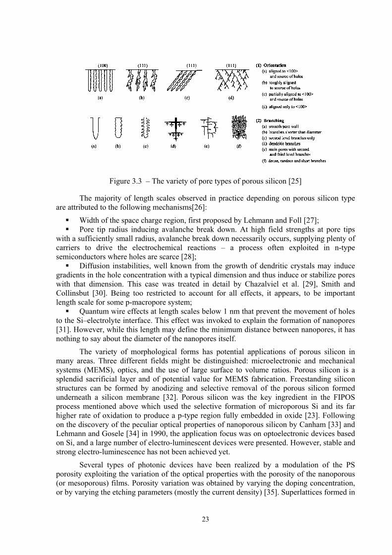
No matter what kind of pore result from experiment, they always have some rather well defined characteristic dimensions like average diameter, average distance, and spacing between branches nuclei. It is safe to say that pore formation of any kind always follows a specific length scale prevalent in the Si – electrolyte system employed and this specific length is expressed in the average pore geometry and morphology (figure 3.3). It should be noted however, that explanation of presence of a specific length scale does not necessarily explain the pore formation itself.
23
Figure 3.3 – The variety of pore types of porous silicon [25]
The majority of length scales observed in practice depending on porous silicon type are attributed to the following mechanisms[26]:
Width of the space charge region, first proposed by Lehmann and Foll [27]; Pore tip radius inducing avalanche break down. At high field strengths at pore tips
with a sufficiently small radius, avalanche break down necessarily occurs, supplying plenty of carriers to drive the electrochemical reactions – a process often exploited in n-type semiconductors where holes are scarce [28]; Diffusion instabilities, well known from the growth of dendritic crystals may induce
gradients in the hole concentration with a typical dimension and thus induce or stabilize pores with that dimension. This case was treated in detail by Chazalviel et al. [29], Smith and Collinsbut [30]. Being too restricted to account for all effects, it appears, to be important length scale for some p-macropore system; Quantum wire effects at length scales below 1 nm that prevent the movement of holes
to the Si–electrolyte interface. This effect was invoked to explain the formation of nanopores [31]. However, while this length may define the minimum distance between nanopores, it has nothing to say about the diameter of the nanopores itself.
The variety of morphological forms has potential applications of porous silicon in many areas. Three different fields might be distinguished: microelectronic and mechanical systems (MEMS), optics, and the use of large surface to volume ratios. Porous silicon is a splendid sacrificial layer and of potential value for MEMS fabrication. Freestanding silicon structures can be formed by anodizing and selective removal of the porous silicon formed underneath a silicon membrane [32]. Porous silicon was the key ingredient in the FIPOS process mentioned above which used the selective formation of microporous Si and its far higher rate of oxidation to produce a p-type region fully embedded in oxide [23]. Following on the discovery of the peculiar optical properties of nanoporous silicon by Canham [33] and Lehmann and Gosele [34] in 1990, the application focus was on optoelectronic devices based on Si, and a large number of electro-luminescent devices were presented. However, stable and strong electro-luminescence has not been achieved yet.
Several types of photonic devices have been realized by a modulation of the PS porosity exploiting the variation of the optical properties with the porosity of the nanoporous (or mesoporous) films. Porosity variation was obtained by varying the doping concentration, or by varying the etching parameters (mostly the current density) [35]. Superlattices formed in

24
this way may be used as high-quality Bragg reflectors, Fabry–Perot filters, waveguides, or antireflection layers. Photonic crystals on a substrate with a textured surface were demonstrated. A way of using microporous silicon as antireflection coating for solar cells has been demonstrated by Striemer and Fauchet [36].
3.2Opticalpropertiesofporoussilicon
As described above, porous silicon represents randomly distributed pores (voids) within remains of silicon (skeleton). The optical properties of the porous silicon will be different from those of bulk silicon. The refractive index (RI) will be a combination of RI at least two phases: silicon (3.5) and air (1) and for as-prepared porous silicon will vary from almost 1.45 up to 3.5 in the near IR. The experimental data for porous silicon with different porosity obtained in [37] is presented on figure 3.4.
Figure 3.4 – Porous silicon refractive index
The simplest porous silicon model is based on an isotropic two-component system, i.e. a silicon carcass and pores with the dimensions much less than the light wavelength. In this case PS can be treated as an optically isotropic medium with an effective refractive index n which is higher than that for air and lower than that for silicon and is a function of porosity. The Bruggeman effective media approximation [38] for multiphase media characterization was found to be in a good agreement with practice in predicting the optical properties of porous silicon. The model is based on additivity of contribution from each phase into effective polarizability of the medium.
211 2
0 (3.3)
where n is the effective refractive index of PS; p is the volume fraction of pores; f – 1p is the silicon volume fraction in porous layer. The solution of the equation gives the variety of RI of porous silicon.

25
It was found that the two-phase Bruggeman approximation is in a good agreement with the experimental data for PS layers on highly-doped substrates [39] [37], but was losing the agreement when moving to the wafers of 0.1… 25 Ω·cm resistance. The reason for that is in the fact that during anodization the surface of the remaining silicon skeleton is partially oxidized. In general decreasing doping level decreases the skeleton dimensions, accordingly increasing the ratio of SiO2 to Si. At the nanometer dimensions (resistances of 10… 20 Ω·cm) the diameter of pores goes down to 1… 2 nm, the influence of the oxide phase becomes more pronounced. Moving towards diluted solutions of HF (water dilution) is expected to increase the oxidation of skeleton as well.
As compared to bulk silicon, porous silicon is also characterized by the shifted absorption wavelength edge towards red part of the visible spectra; highly porous films are more transparent in this part. This is partially attributed to the band gap widening of the porous silicon and quantum effects. Due to skeleton depletion nanosized porous silicon has lower free-carrier absorption respect the initial bulk silicon.
3.3Oxidizedporoussilicon
Unfortunately, the developed structure of porous silicon with high surface area leads to low stability of its optical properties in time, especially for highly porous structure. During time, being subjected to ambient, the skeleton of porous silicon is uncontrollably oxidized and absorbs other impurities. In order to prevent aging a stabilizing of porous silicon skeleton can be performed by oxidation of its surface. Due to well-developed structure the oxidation of porous silicon is a fast process with low thermal budget. Oxidation temperatures as low as 200°C are possible. Authors of [40] by analyzing the IR absorption peaks have found that below 400°C the Si2O3 oxide was also formed, while the 500°C and higher lead to pure SiO2 formation. Usually the stoichiometric composition of the oxide is unknown, but according to some authors the ratio between silicon and oxygen corresponds to SiO2, other authors believe that the ratio varies with the layer depth. As the oxidation step changes optical parameters of the layer, care must be taken in choosing the initial porosity if exact optical values of refractive index are a target.
The oxidation of porous silicon in oxygen atmosphere proceeds with a well-known reaction:
(3.4)
Thermal oxide obtained incorporates silicon consumed from the substrate and oxygen
supplied from the ambient. Thus, it grows both into the wafer and out of it. For every unit thickness of silicon consumed, 2.27 unit thicknesses of oxide will appear. Moreover 44% of the oxide thickness will lie below the original surface, and 56% above it. It means that during oxidation, porous silicon skeleton will be converting to oxide starting from the surface of crystallites and after a certain time the maximum oxidation degree will be reached as soon as the entire skeleton is converted or the oxidized pores collapse. The maximum oxidation degree form is obviously the most stable form of oxidized porous silicon. Depending on the initial structure the oxidation will result in several types of materials. Obviously there exists only one value of “optimum” porosity (in fact it is 56%) that will be able to undergo complete oxidation that will result in a compact silicon dioxide layer. Such layers will obtain the best

26
electrical and optical characteristics, with low-loss even in visible range of optical spectra [41]. Layers with lower and higher values of porosity after oxidation will be rich with silicon crystallites or voids (porous oxide) correspondingly. Optical layers of this kind will obviously have increased optical losses due to scattering on the voids of crystallites. Nevertheless, all kinds of oxidized porous silicon can be used as optical layers in silicon photonics.
A modified Bruggeman equation can be used for describing the oxidized porous silicon as a three-component medium, consisting of silicon, oxide and pores [42]. By accepting that the oxidation of the internal pore surface takes place throughout the entire film thickness and results in the formation of silicon dioxide with the refractive index n= 1.46. Bonding of silicon with oxygen produces a 2.27x volume rise of the solid carcass. Since the density of Si and SiO2 have nearly the same value (2.3 and 2.2 g/cm3), the gravimetrically measured porosity does not practically depend on the solid carcass content and gives more or less accurate porosity value.
2.27 1 1.27 0, where
(3.5)
2
,2
,11 2
(3.6)
From where it is possible to deduct the fraction of silicon being used for SiO2 and then deduct a new porosity value after oxidation
1
2.27 1.27 (3.7)
1 1.27 1.27 (3.8)
The variety of the refractive index and structure can be seen from fig 3.5. It can be seen, that oxidation always decreases the refractive index value. Porous silicon films with lower porosity undergo higher refractive index change, while high porosity layers are less sensitive to oxidation. Porous silicon layers with different initial porosity behave differently during oxidizing.

27
Figure 3.5 – Refractive index of oxidized porous silicon depending on initial porosity and oxidation degree
The layer with > 56% remains porous even after a complete oxidation, whereas those with lower porosity can lose the pore structure long before the total oxidation. The pore disappearance transforms the material into another two-component system Si – SiO2, its oxidation degree being independent of the initial porosity.
3.4Scatteringinporoussiliconandoxidizedporoussilicon
Oxidation is a critical step of obtaining the high-quality material. If as-prepared porous silicon is subjected to high temperature treatment in oxygen atmosphere with a high temperature ramp a sintering happens leading to coarsening of pores. The effect has been observed by many groups [43], [44]. The pores dimensions size can increase by several times.
Figure 3.6 – Sintering of mesoporous silicon
This can be a critical issue as the pore size approached the effective wavelength λ′ = λ/nSi = 1550 nm/3.5 = 442 nm, or λ′ =λ/nSiO2 = 1550/1.44 = 1076 nm. A detailed influence of the scattering voids has been given in the work [45]. While performing optical characterization of sintered porous silicon films, the absorption level was found to be much higher than that one of pure silicon deducting that scattering is the main contributor. By

28
applying the Mie’s theory [46] considering the pores of sintered porous silicon close to spherical has found the efficiency of scattering significant (figure 3.7).
Figure 3.7 – Scattering efficiency of spherical voids embedded in bulk silicon for different wavelengths. Scattering coefficient of vacuum voids embedded in bulk silicon for different
distributions. The porosity is P =30%. For comparison, the band-to-band absorption coefficient αgen of bulk silicon from as well as the free-carrier absorption coefficient αFC for
p=8·1018 cm−3 are plotted as dashed lines
It was also found that effective medium models, which are frequently used to describe the optical constants of as-etched PS, also comply well with the refractive index of sintered PS. In the visible range, the refractive index of OPS agrees with predictions of the Bruggeman or the linear model, whereas in the IR, the Maxwell Garnett formula gives a better match. Mie’s theory enables the quantitative description of light scattering by the spherical pores in SPS. The comparison of measured and calculated scattering coefficients reveals that in sintered OPS, the close spacing of the pores reduces the scattering efficiency of the individual spheres. The performed analysis shows that, when accounting for adjacent pores by using a reduced refractive index for the host medium in Mie’s theory, the measured and calculated scattering coefficients agree.
3.5Notesonoxidationofporoussilicon
Though the oxidation of silicon in oxygen atmosphere proceeds with a well-known reaction, porous silicon thermal treatment has some peculiarities. It was pointed out that some complicated structural changes are observed if the porous silicon is subjected to high temperatures immediately after preparation. For example if performing oxidation of as-prepared samples, the porous silicon structure changes easily under thermal treatment, leading to a material formed by larger pores and thicker silicon rods, i.e. sintered porous silicon. The structural changes are believed to be caused by the high specific surface of the material. The very large specific surface area of 200 cm2/cm3 [47] implies a large surface energy. For example, the surface energy of a sample of 1 cm2 with a 10 μm thick porous film is 0.2 J which has to be compared to 1 – 4 J for the solid surface free energy. This suggests that upon heating, this surface energy can be decreased by surface diffusion of silicon atoms, leading to coalescence of pores and reduction of surface energy. This porous silicon sintering may lead to unwanted changes that will influence the oxidation process and even hurdle the complete

29
oxidation of silicon skeleton on the way of obtaining optically perfect silicon oxide leaving unwanted voids. It was found experimentally that this structure evolution can be avoided by growing a thin silicon dioxide layer on the pore walls before the thermal treatment, in other words doing peroxidation step. This thin silicon dioxide layer present on the pore walls hinders the change of surface area due to reducing the diffusion of silicon atoms. The temperature of the peroxidation lies in the range of 300… 450 °C. This preoxidation step allows thermal treatment at high temperatures without significant porous microstructure changes. In order to obtain the fastest oxidation rates the oxidation is often performed in the wet ambient at temperatures reaching 1000 °C. The quality of completely oxidized porous silicon films was found to be comparable of that of grown silicon dioxide.
3.6Singlemodefibercouplingusingporoussiliconstructure
Silicon photonics exhibits an extremely high level of functional integration due to the very small cross sections of the silicon waveguides with less than 1 micron Mode Field Diameter (MFD). However, to be successfully implemented in data optical transmission networks, such circuits must be interfaced with single-mode fiber optics generally having 10 times larger dimensions (for example, Corning SMF-28 ULL has 8.2 μm core corresponding to MFD of 10.5 ± 0.5 μm). Due to this mismatch, a coupling structure is required to adapt a wide SMF mode with a narrow silicon photonics waveguide mode to avoid high losses that are crucial for the optical link performances.
Two approaches are exploited for low-loss coupling. Out-of-plane coupling based on grating requires small foot print area and can provide losses well below 3 dB, but is a narrow-band and quite sensitive to tilt. In-plane butt coupling is an easier technology, but requires a focusing system or lensed fibers and is very sensitive to alignment of focusing system otherwise introduces 10 dB of losses and more. In-plane tapering structures could achieve losses well below 1 dB and are less alignment sensitive but being generally bidimensional are limited to layers with homogeneous optical properties thus extending for long (>300 micron) distances and still suffer heavily from misalignment. Moreover, in order to be compatible with functions for fiber-to-the-home (FTTH) or wavelength division multiplexing (WDM) applications a coupling structure is also required being broadband and polarization insensitive. Finally, aside from the performance, the selection of the optical coupler is also driven by the cost issue considering the wafer-level testing capability and the packaging requirements for the fibers assembling and the thermal management.
The promising approach for a mode size conversion is utilization of graded refractive index (GRIN) structures [48]. Unfortunately current fabrication technology is quite complex and mainly lies in consequent deposition of thin layers with different refractive indexes. While suitable for vertical transformation of the mode size, the lateral mode field conversion is not an easy task. Also, being limited to a RI gradient only in vertical direction, the effective RI of such GRIN structure usually significantly exceeds that one of the SMF and reflection issues arise.
In order to achieve a good matching with both SMF and SPWG a tapering structure based on porous silicon can be realized characterized by a spatial variation of geometry and refractive index of optical layer forming a GRIN media allowing simultaneous conversion both of the vertical and lateral mode sizes. The simplified design of the developed taper is presented on figure 3.8. At one end of the taper a V-groove is fabricated allowing a

30
mechanically stable alignment of the cleaved SMF with error not exceeding couple of μm. The V-groove is followed by a tapering coupler structure with has a well-defined core and cladding layers.
Figure 3.8 – A proposed 3D tapered coupler design
The optical tapering structure itself can be fabricated utilizing oxidized porous silicon technology which has already been proven to be a suitable material for silicon photonics. As the layers of porous silicon are obtained by a simple electrochemical anodization of silicon surface in HF-based solution, the resulting thickness and morphology (structure, porosity) is governed by processing parameters (i.e. time and anodization current density). The difference in morphology leads to a difference in optical properties after the oxidation step. The possible refractive index of the obtained OPS layers starts from 1.45 in case of the total oxidation (low to medium porosities) and almost reaches that one of pure silicon (in case of low porosities) allowing modulation of optical parameters. The 3D variation of optical properties can be created utilizing the dynamic liquid meniscus (DLM) approach [49]. The working principles of the DLM are explained on figure 3.9
Figure 3.9 – DLM processing principles
A special head is designed having the nozzle and two inlets. The electrolyte is continuously jetted towards the substrate through the nozzle and simultaneously recalled back into the head by creating the depression of the air in the inlets. Preserving the balance between the jet and the depression allows for a small self-sustaining drop formation. The size of the drop is defined by the nozzle geometry (length and width). Such a drop brought in touch with

31
the substrate created a dynamic meniscus that resembles a small electrochemical cell with constantly refreshed solution avoiding the necessity of having the rigid walls or sealing. Applying the potential to the electrolyte with the help of cathode permits localized conversion of silicon surface to porous silicon inside the meniscus area only. Movement of the head along the surface at a certain speed together with modulation of current density permits 3D variation of porous silicon morphology and thus optical parameters after oxidation.
The tapering can be fabricated by anodization through an opening in Si3N4 mask corresponding to the core shape. In order to fabricate the core and the cladding beneath it with 3D variation of RI a number of passes is performed, each pass resulting in formation of a layer of the chosen thickness and RI distribution.
The initial dimensions of the taper core are chosen to be higher than the MFD of the fiber thus to minimize possible the alignment errors due to WG insertion in the groove. The effective RI of the taper core at the SMF input is close to 1.45 allowing a good match with the fiber. As the light propagates through the structure the MFD is gradually decreased and the optical power is brought closer to the surface. This is achieved by a gradual increase of the RI index jump between the core and the cladding layer and simultaneous adiabatic shrinking of the core size in both dimensions thus leading to both vertical and lateral compression of the MFD (figure 3.10).
Figure 3.10 – Cross-section (top) and top (bottom) views of the Gaussian beam propagation in the developed taper
As can be seen from numerical simulations for a taper with 200 μm length it is enough for core RI to go from 1.45 up to 1.75, to allow the MFD to be reduced simultaneously laterally and vertically and to be also shifted towards the surface with good confinement. Optical power can then it can be much easily collected by a tapered SPWG. It will be shown that the losses can be reduced to less than 0.2 dB by choosing the optimum length and RI gradient.
The coupler can be realized within the volume of silicon wafer. Accepting the orientation of the starting wafers 100 the V-groove is done by anisotropic KOH wet etching process, resulting in a pyramidal recess with the sidewall angle of 57.4° due to high selectivity of 111 to 100 plane etching. In contract to DRIE producing scalloping, the KOH etching results in very smooth sidewalls allowing to avoid scattering.

32
Localized electrochemical treatment technique using DLD implemented for silicon anodization reveals a unique possibility for realizing OPS structures with a 3D variation of optical properties. Using the DLM approach for OPS fabrication it is possible to realize the optical backplane substrate including the set of essential components (i.e. silicon waveguides, fiber coupling and out-of-plane input/output). The possibility of direct coupling with a vertical cavity surface emitting lasers, optical signal rerouting to output fibers and distribution between SP chips with low losses, high thermal stability and high bandwidth and the possible approach of using such substrate as a multi-chip-module (MCM) for die soldering of the SP and driving integrated circuits chips, opens up the route to low-cost MCM optical backplanes for silicon photonics.
Summaryofthechapter3
Porous silicon can be considered as a way of expanding the optical properties range of silicon. It can be utilized in as-prepared (but less stable) material with refractive index being in between that one of bulk silicon and air, with acceptable level of optical losses due to scattering. A more stable form is obtained by stabilizing the highly reactive silicon skeleton by its partial or complete oxidation that is characterized by lower refractive index in general. Resulting material is oxidized porous silicon – a combination of silicon, SiO2 and air, or, if the initial porosity is chosen close to 56%, the compact silicon dioxide. Layers with lower and higher values of porosity after oxidation will be rich with silicon crystallites or voids (porous oxide) correspondingly and will obviously have increased optical losses due to scattering on the voids of crystallites. Nevertheless, all kinds of oxidized porous silicon can be potentially used as optical layers in silicon photonics.
Care must be taken in oxidation steps of porous silicon. Before the high temperature process a first oxidation step must be performed at low temperature (300… 400 °C) to stabilize the structure of porous silicon by slightly oxidizing the skeleton. Otherwise a sintering may happen leading to pore coarsening and high scattering absorption in the resulting oxidized porous silicon film.
In general the ability of manipulating the optical properties of porous silicon by mere changing of technological conditions of fabrication makes this material a very attractive from the point of view of silicon photonics. Layers of porous silicon with different porosity and structure and thus with variety of refractive index values can be obtained by changing such parameters as current density, external light intensity, anodization electrolyte composition or by choosing the substrate doping levels. Porous silicon layers with different optical properties can be used as antireflection coatings, waveguides, optical ring resonators and various kinds of interference filters.

33
4Natureofsilicondissolution
Porous silicon formed by different groups under virtually the same experimental conditions may hardly be comparable. No wonder that till now controversial views exist on the formation mechanisms of porous silicon. Until now only general knowledge exists about experimental parameters determining PS morphology and properties.
4.1Chemistryandthermodynamics
Porous silicon is obtained by the electrochemical treatment in the solutions containing HF under anodic polarization. If we perform a CVA of the Si-HF system we will obtain the typical IV curve similar to the one from figure [25]. The behavior of the current is similar to all the systems where the porous silicon if created.
Figure 4.1 – A typical IV curve for silicon in HF at anodic polarization
Several characteristic regions with different resulting materials can be distinguished on the curve. Starting from the open circuit potential at small anodic overpotentials, the current increases exponentially with electrode potential. At a certain potential the current growth becomes almost linear. As the potential is increased further, the current reaches a peak (critical current) after which remains relatively constant. The critical current density value and position varies with HF concentration, temperature, hydrodynamics [50] and type of solvent used. In some solvents, e.g. water and ethanol, more than one peak is present [51]. The different regions are similar for other fluoride containing solutions of various compositions and pH values.
It was found that porous silicon forms in the exponential region. Examination of the sample surfaces that are anodized at different potentials indicates that the potential corresponding to the maximum slope of the IV curve is the upper limit for formation of uniform porous silicon layer. In the range between the maximum slope and critical current, porous layer still growth but the surface coverage is not uniform, decreasing as the potential approaches the peak value. Electrochemical polishing occurs at potentials higher than the peak potential. Thus the peak current separates the region of porous silicon formation and electropolishing.

34
During the anodization hydrogen evolution occurs simultaneously throughout the full range but its rate decreases with potential and almost ceases above the peak value. It was also found that changing current changes the dissolution valence from about 2 to almost 4 being the evidence that various reactions paths are taking place at different potential. A good explanation of the silicon behavior under anodic polarization was summarized in [25]. Silicon is thermodynamically unstable in air or water, and it reacts spontaneously to form an oxide layer. The oxide can be nonstoichiometric and hydrated to various degrees, though the simple empirical formula is silicon dioxide, SiO2.
→ (4.1)
The reaction of silicon with water should be analogous to the reaction of metallic sodium with water: elemental silicon is electropositive enough to spontaneously liberate hydrogen from water. However, silicon does not dissolve in acidic solutions, even if the solution contains fluoride ion to remove the passivating SiO2 layer. Although thermodynamically feasible, dissolution of silicon in aqueous HF is slow unless strong oxidizing agents (such as O2 or NO3
−) are present in the solution, or unless the oxidation reaction is driven by electrochemistry. The reason is that corrosion becomes kinetically limited by passivating surface with hydrides [52].
Thus in order for dissolution to proceed requires the replacement of the hydrogen first by F from HF is necessary. This replacement requires a hole that leads to neutralization by the Si-F bonding (Figure 4.2).
Figure 4.2 – Silicon dissolution paths in HF containing electrolytes
The valence state of hydrogen atom does not change during this process and remains zero. On the other hand the hydrogen absorption on the Si surface is a reduction process requiring electron since the valence changes from 0 to +1. It occurs when the Si-SiF bond is broken by reacting with HF (path I). A feature of the step 2 is that no carriers are involved from the solid although it is an oxidation process for the silicon atom involved (from valence 2 to 4) and therefore it is chemical process by nature. This is a key step responsible for the chemical character of the dissolution process in that in the process of becoming adsorbed a hydrogen ion is reduced by receiving an electron from the Si-SiF bond. In this way the occurrence of different regions during anodization of silicon in HF solutions is associated with the two competing reaction paths: direct and indirect dissolution of silicon oxide the

35
balance between them changes with the potential. The reaction path I results in the direct dissolution with valence 2 of silicon path II is indirect dissolution and results in the dissolution valence of 4.
The net reaction by two paths can be approximated by following equations [53].
6 2 2 porous silicon
6 4 4 electropolishing
Below the peak current, the kinetics (or charge transfer) is the limiting step. This means that fluoride species are abundant at the interface because they are not consumed as fast as they get diffused towards the interface. The peak potential where the critical current density resides is believed to be both diffusion-controlled and kinetics-controlled. Both diffusion and kinetic current contributes to the total current. Beyond the peak current, diffusion (or mass transfer) is the limiting step. Silicon reacts with water molecules faster than fluoride species, forming oxides that are eventually etched by HF species [54]. Shifting to more positive potential than peak current the surface is completely covered with an oxide film and thus anodic reaction proceeds through the formation and dissolution of oxide, the rate of which depends strongly on HF concentration. At very high potentials and low HF concentrations oxide forms faster than it is being dissolved, resulting to oxide build up [55]. Electropolishing region does not occur in anhydrous organic solutions due to the lack of water which is required for the formation of oxide film.
The mechanisms described above give an insight on the chemistry of silicon dissolution. Still in order a porous structure to be created the reaction should be localized on the pore tips, it means that wall of the remaining skeleton should be passivated during the anodization process (like RIE Bosch process), otherwise all the layer would be uniformly etched away. Two main explanations currently exist: a quantum confinement and space charge region. In fast as the porous silicon start to form, a skeleton being narrow (few nm) leads to local increase of the carrier energy due to quantum confinement, thus leading to some increase of the band gap. This leads to depletion the wall with free carriers and passivation of the skeleton walls and preferential etching on the pore tip. The second theory is related to a space charge region existence on the skeleton. As the silicon becomes depleted by charge carriers the electrochemical oxidation can no longer proceed and the walls become passivated.
During PS formation at an anodic potential, the tip of pores dissolves preferentially due to easy excess to holes. The pore wall areas, which are sufficiently distant from the tips, have no holes available, dissolve chemically at a very low rate. The chemical dissolution does not depend on potential but on the time of immersion and the total surface area of the PS. However, although the dissolution rate is very low, a significant amount of material may be removed by the chemical dissolution during the formation period of PS due to the large surface area of PS. Chemical dissolution is responsible for the dissolution valence lower than 2 and the change of PS density with depth.

36
4.2Poroussiliconinpractice
In order for obtaining porous silicon a simple two-electrode system is often utilized. The anodizing process is quite stable and once being tuned (kinetics dependencies and porosity curve measured) the results are predictable. In this case the galavanostatic (constant current) mode of fabrication is a simplest way of controlling the PS layer thickness and porosity. In case of the localized fabrication of porous silicon a need to switch to three-electrode system arise as the pores will follow the current density lines and the anodization front (area) will change during the time. In this case keeping the process predictable is only possible by constant potential and charge measurements during the anodization.
Figure 4.3 – A typical anodization setup
The stable anodizing process is usually observed in the range of 2…5 mA/cm2 to 100 mA/cm2. The formation of porous silicon is possible at the range of current densities that lie below critical current density value, after which the process transform to electropolishing. The critical current density value depends on the solution concentration: for example in 6% HF solution the critical value is only 60 mA/cm2, while in concentrated HF:IP solution reaches 600 mA/cm2 and higher [28]. The anodization rate and porosity in general are proportional to the current density, except for low current density range when the chemical oxidation rate is comparable to the electrochemical dissolution and the porosity tends to increase. Therefore a porosity minimum always exists on the PS/IV curve. Addition of wetting agents (isopropanol is widely used one) will allow to overcome the diffusion limitations and somewhat stabilize the porous silicon porosity in wider current density range.
Temperature of HF solutions generally has little influence on growth rate of PS [56] thought it changes the balance between electrochemical and chemical dissolution and thus influences the porosity of the resulting material, usually tends to increase with lower temperatures [57]. PS growth rate is generally higher on (100) substrates than on (111) substrates. The growth rate of a PS layer can vary over a wide range depending on formation conditions. It can be as low as a few A/s and as high as 4000 A/s. PS thickness increases linearly with time up to certain thickness. Such constant growth rate at a constant current density means that the PS formed is uniform in thickness. In practice the layers of 10…20 μm are obtained without any problems and significant change of porosity respect the surface. Still it is possible to obtain thicknesses up to several hundreds of μm. At a large thickness the growth tends to deviate from linearity due to the effect of diffusion in the electrolyte within the pores. It has been found that for a very thick PS layer (150 μm) there is about 20%

37
difference in HF concentration between that at the tips of pores and that in the bulk solution that leads to difference in porosity.
The characteristics of the IV curves are quite identical for all types of materials except for low-doped. For low-doped n-Si, it requires a large polarization or illumination to generate anodic reaction as the surface is under a reverse bias as shown in Figure 4.4.
Figure 4.4 – The difference in behavior of n and p-type Si in HF solution from [58]
The dependence of IV characteristics on doping is an indication of the carrier conduction mechanisms that can occur in a silicon substrate. When carrier supply in the silicon substrate is not rate limiting, IV curves obtained in different HF concentrations are identical in characteristics. When the supply of carriers in the substrate is rate limiting as determined by the doping and illumination condition, IV curves display distinct difference between p-type and n-type silicon, and for n-type between illuminated and non-illuminated materials. For non-heavily doped p-type silicon, the process is by thermal emission of holes while it is by Zener tunneling for heavily doped materials. For moderately doped n-type the reaction is limited by the minority holes; significant current occurs when a large amount of holes are generated by illumination or when relatively high anodic potentials are applied to allow interface tunneling to occur that will be discussed later.
Thus the behavior of PS formation is different on n and p-type wafers. For p-type Si the growth rate of PS at a given current density increases linearly with HF concentration and current density. For n-Si the growth rate increases also with HF concentration and current density but the relations are not linear. Also, for p-type silicon, it increases linearly with logarithmic dopant concentration but for n-type Si the dependence of growth rate on dopant concentration is more complicated. Anodic dissolution of n-type Si proceeds at a polarization under illumination. The maximum current is limited by illumination intensity when the saturation photo current density is lower than the critical current. The characteristics of IV curves of n-type under high illumination intensity, when the reaction is no longer limited by the availability of photo generated carriers, is identical to that for p-type. Similar also to p-Si, formation of PS on n-Si occurs only below the critical current.

38
In general low current density and high HF concentration favor PS formation while high current and low HF concentration favors polishing. The relationship between current and potential is linear due to the rate limiting effect of resistance in solution and silicon substrate.
4.3Poroussilicondissolutionroughness
Little information on the PS/Si dissolution interface the roughness exists. A detailed investigation of the dissolution interface roughness was given in the work [59]. Two types of fluctuations were revealed, one at the millimeter scale (waviness) and the other one at the micrometer scale (roughness), RMS amplitudes of both were comparable. The large scale fluctuations were attributed to planar resistivity fluctuations in the wafer. The RMS values as high as 8... 9 nm were registered at 4 um porous silicon layers. The roughness was found to increase linearly with the layer thickness up to a critical value where a saturation regime was observed. No effect of the hydrofluoric acid concentration on the roughness was observed. Comparable roughness parameters were measured for PS layers of 51% and 70% porosity corresponding to HF of 22.5% and 12.5% respectively. For low doped PS layer formation on the roughness amplitude for two layer thicknesses strongly decreased with increasing current density and no further variation was observed above 70 mA/cm2. The decrease of the RMS amplitude with increasing current density was explained by approaching to electropolishing current density. But this could not explain the fact that the saturation of the current density was observed long before reaching the critical current density and the increase of roughness with the time. An influence of the solution viscosity was revealed as well. A significant reduction of the RMS by a factor of 2.5 was observed after changing the viscosity by replacing ethanol with heavier alcohol octanol whereas other layer characteristics were not changed.
More detailed investigation of the electrolyte viscosity during electrochemical etching of p-type porous silicon (PS) at room temperature was given in the work [60]. The roughness was measured in-situ with the help of interferometric measurements of interface roughness in-situ. It was found that for a porosity value of 70% and with an electrolyte where a low fraction 10% of the ethanol was replaced with glycerol, there was a significant decrease of the interface roughness. However, a higher content of glycerol (>10%) increased the surface roughness. It was also found that the porosity of the PS varied only slightly when glycerol at various concentrations was used.
The advantage of using heavier alcohols is unfortunately hindered by their not perfect mixing with the other components of the electrolyte, resulting in rather inhomogeneous samples.
It was found that temperature also has an influence on the porous silicon dissolution interface [61] when using low-doped (8 Ω·cm) p-type silicon wafers (figure 4.5). The lower roughness observed at low temperature was attributed to the reduction of the critical current. As a consequence the same current intensity at low temperature will be closer to critical current and smoother interfaces are explained. These results are reasonable if we consider that moving toward the electropolishing region the process undergoes change from the reaction-controlled to diffusion-controlled. As the diffusion rate strongly depends on the temperature obviously the processing at lower temperatures will lead to decrease of the critical current density.

39
Figure 4.5 – Variation of the roughness as a function of the PS thickness at 26°C and -35°C for current densities of 16.6 mA/cm2 (a), 166 mA/cm2 (b), and 333 mA/cm2 (c) from [61]
The viscosity of the solution plays the same role on the diffusion rate. While porosity in principle is controlled by characteristic length that mainly depend on the substrate parameters and external electric field. In this was no big influence of viscosity and temperature on the porosity should be observed.
It was found that the size of the pores in microporous silicon was smaller than the typical dimension of fluctuations for all doping levels of the substrate. It was also assumed that the dissolution roughness is not directly induced by the porous nature of the material.
Summaryofthechapter4
Porous silicon is a material obtained by conversion of bulk silicon substrate in electrolytes containing fluoride ion (usually HF-based) under anodic polarization. Conversion of silicon into porous silicon by anodic treatment is a complex combination of chemical and electrochemical processes; the primary reaction is electrochemical oxidation or dissolution. The reaction requires the charge transfer through the boundary Si-HF, the holes are required to break Si-Si bonds. It means that the process will follow the current density lines and depends on the availability of holes at the interface, i.e. selective to doping of silicon. Protection of the silicon substrate surface from the flow of the current by masking is sufficient to avoid the conversion of the surface to porous silicon. Using substrates with areas of different doping silicon substrate can be selectively conversion into porous material.
An attractive platform comes in mind where the standard CMOS wafer is used as a starting platform for integration of SP, IC and MEMS devices. By using wet anodic treatment the substrate is locally converted into porous silicon. Porous silicon in turn can be converted to silicon oxide for complete electrical and optical isolation from the substrate, or can be used as a material whose properties can be modulated by the processing required for realizing Bragg reflectors and couplers. Porous silicon can also be used as a sacrificial layer meaning subsequent removal for releasing the parts of MEMS devices. Such a platform will allow a unique integration of most of the components directly on the chip and will be completely compatible with CMOS technologies.

40
5LocalizationofporoussiliconPorous silicon is a current flow driven process. Under the anodic bias the surface of
silicon subjected into HF electrolyte will be converted into porous layer. The conversion proceeds towards the contact that is injecting charge carriers into silicon and follows the current density lines.
In order for realizing the localized SOI substrate or using the porous silicon as a sacrificial layer a formation of porous silicon must be restricted to the areas of interest only, leaving the rest of the surface undamaged. This can only be done by appropriate masking for preventing current flow through the areas that have to be protected and only understanding the peculiarities of the porous silicon growth.
5.1Planarmaskingapproach
The only way of fabricating porous silicon locally on the silicon substrate is to use proper masking technique that will limit the current flow and consequently porous silicon growth only to the area of interest. The masking material can be chosen from the range of etch-resistant materials like dielectrics (photoresist or LPCVD silicon nitride), semiconductors (low-doped or “properly” doped) and metals (mainly noble). Processes with Si3N4 mask are limited in time as nitride is etched with the rate of about 10 – 15 nm/min [62], and the maximum thickness is limited by internal stress to about 200 nm. Processing times of 10 minutes are possible in concentrated HF. Time can be significantly enlarged by going for less concentrated solution or by reducing the anodizing temperature (about 2… 4 times gain each 10 degrees) [63]. Photoresist masking should be used with care especially for the HF:IP mixtures. Isopropanol commonly used as a wetting agent attacks the photoresist and may lead to strong underetching due to high liquid permittivity and even delamination. Silicon dioxide can also be used for low thickness layers [64] or with some modifications to the electrolyte (like addition of PEG, for example) significantly reducing the etching rate of SiO2. Good results were obtained with undoped polycrystalline silicon masks.
Apart from dielectric, conductive mask can be used from noble metals and some others that are stable in HF due to passivation like Mo, Co and Nickel can be potentially used as well.
Depending on the choice of the masking material, a different etching shape is observed. In general as the growth of porous silicon follows the current density lines, there will always be some underetching as the current lines will decline from under the masked areas towards the openings. Apart from pure anisotropic behavior, side effects are observed when an insulating masking layer is used on the low-doped n-type silicon. In this case a carrier inversion due to negative potential of the solution respect the substrate may occur under the masking area, and then more holes become available that can easily drift to the open areas in the masking layers. This causes a wide undercutting of the masking (up to hundreds of micrometers see figure 5.1A (taken from [32]). For the low-doped p-type silicon the negative potential cause local increase of the holes concentration as well leading to significant undercut depending on the fabrication conditions. Generally for insulating masking layers, the layer thickness at the edges is higher than in the center of the etched structure. The inhomogeneity originates from the higher concentration of electric field on the border of the masking layer (figure 5.1B). This nonuniformity can be significantly reduced by using

41
electrically conductive masking layer since part of the current from the substrate will flow through the metal to the solution without concentrating completely on the opening in the masking layer (figure 5.1C).
Figure 5.1 – Influence of the masking layer and the substrate doping on the etching behavior
A typical porous silicon profile obtained with a planar masking is presented on figure 5.2a. Exploiting high reactivity of PS respect bulk silicon etching in diluted KOH solution can be used to selectively remove the anodized layer exposing the silicon surface (figure 5.2b). This process is widely used in MEMS fabrication via porous silicon technology.
a b
Figure 5.2 – A typical shape of the porous silicon obtained with Si3N4 mask on highly-doped wafers (left) and selectively etched (right)
In general the anodization process can be considered isotropic, that means that for planar masking the undercutting is in the same order of magnitude as the etch depth. The underetching rate will depend mainly on the openings geometry, opened area ratio, the doping of the substrate and some other factors. Usually the underetching value is in the same range as the porous silicon layer thickness (lower by the factor of 0.7… 0.8), i.e. the etching for 10 μm depth will also laterally extend to the 7... 10 μm in both directions (figure 5.3).

42
Figure 5.3 – Underetching of porous silicon below the silicon mask protected with polycrystalline silicon layer
Underetching leads also to the change of the real anodizing area and thus real effective current density during the process and if not taken into account will lead to changing of porosity (decrease) and etching rate as the process proceeds. This issue is critical when the opening area is comparable to the target depth.
5.2Three‐dimensionalmaskingapproach
More complex structures can be obtained if part of the silicon substrate itself becomes a mask for the anodization process. This can be done utilizing the sensitivity of the anodization process to doping level of the substrate (availability of charge carriers) and defects. In this case a main approach is to protect part of the substrate by converting it into material that will not undergo electrochemical etching at low potential.
5.2.1Maskingbydoping
Silicon masking can also be done by utilizing the doping sensitivity of the anodization process (figure 5.1D) [23]. Since the silicon anodization rate is mainly controlled by the availability of holes at the silicon-solution interface, a good selectivity is obtained between n-type and p-type silicon and between low-doped and highly doped p-type [65], [66]. When the doping energy is small, the behavior is similar to that one with the metal masking. Moreover a p-type masking can be used for n-doped substrates, as the reverse p-n junction will prevent holes from reaching the interface as no carrier transport through the p-n junction under the reverse bias will be observed.
A localized doped region can be realized by diffusion or by ion implantation.

43
Figure 5.4 – Distribution of dopant by diffusion (a) and implantation (b)
Diffusion can be done by heating silicon substrate in contact with gaseous, liquid, and solid media. Diffusion is a high-temperature process by definition. While ion implantation is introducing dopant ions by high energy bombardment and is performed as low temperatures even using photoresist mask. An implanted ion undergoes scattering events with electrons and atoms in the target, reducing the ion's energy until it comes to rest, the total path length of the ion is called the range, R. The depth of implantation is proportional to the ion energy and dose can be precisely controlled. The projected range and straggle of the Gaussian distribution give a good first-order description of the implanted ions in amorphous or fine-grain polycrystalline substrates. The dopant's depth distribution profile can be well-controlled and by combining several implantation steps complex doping profiles can be built.
Figure 5.5 – A typical distribution of implanted ions in silicon
But besides that the implantation itself provides more freedom than a planar masking. Indeed by modulating the implantation energy the masked region can stretch up to several tenths of micrometers into the bulk silicon. Anodization of such structures will allow a three-dimensional modulation of the porous silicon process flow and creation of various structures. Porous silicon can then be etched away selectively respect silicon or converted to silicon dioxide. Masking by doping was used for silicon MEMS structures fabrication, membranes, beams and cantilevers [67]. Usual dopant for silicon are As and P (for n-type) and B for p-type. Multiple implantations are possible to compensate the existing dopant and invert the conductivity type.

44
5.2.2Maskingbyprotonimplantation
Apart from standard implants being donors and acceptors a process of hydrogen (proton) implantation in silicon was found to seriously influence the electrical characteristics of this material [23].
Though hydrogen itself is not an acceptor or donor it can influence significantly the concentration of free carriers by passivation of deep and shallow impurities [68][69], by formation of shallow donors [70]. If thermal annealing is performed on the as-implanted samples thermal donors formation leading to inversion of the conduction type (from p to n)is observed in the range of temperatures of about 300… 500°C by interacting with the oxygen that always is present in silicon wafers. The latter process is not directly related to implantation parameters but depends on the oxygen concentration in the starting wafers, and thus can be considered as unreliable. Still diode structures with shallow [71] and deep p-n junctions obtained at relatively low temperatures on Cz wafers [72] were reported.
Thus depending on the dose ion irradiation of silicon introduces lattice damage as vacancy-interstitial pairs. The number of Frenkel defects produced along the initial portion of the trajectories is fairly constant and then increases sharply towards the end-of-range. This defects influence the distribution of the carriers and thus formation rate of porous silicon. They can act favoring porous silicon formation and at the certain levels were found to increase the PS formation rate (or change its structure). Also after a certain dose the number of the defects-related traps increase is significant for creating traps in the forbidden band and thus significantly influence the carries transport due to recombination through deep-level energy states thus reducing the hole density and increasing the resistivity of the irradiated region. Under high dose the porous silicon formation rate was found to decrease and to stop completely [73].
Several other types of “inert” ions like Si, Ga, O were found to be capable of modulating the PS formation rate. Ions are deflected by many collisions with atomic electrons, resulting in an increase in beam spot size with depth that is more significant for heavy ions. Ion irradiation of silicon introduces lattice damage as vacancy-interstitial pairs Frenkel defects along the ion trajectory. If taking into account of applications of the structures after the implantation step, defects caused by implantation of heavy ions are more intense and extremely difficult to recover even at long annealing. From this point of view proton implantation can be considered as an attractive step. For example the process is utilized for SOI SMARTCUT process proving that negative effects of hydrogen implantation are completely removed.
If we compare the straggle of H and P (figure 5.6), we can see that the hydrogen will allow much narrower peak that will potentially result in better control for creating shallow areas (for silicon photonics) and potentially will produce less roughness.

45
Figure 5.6 – A comparison of defects caused by Hydrogen (left) and Phosphorus (right) implantation for 220 nm target depth using TRIM simulaton
The feasibility of patterning with focused proton beams was first demonstrated by Polesello et al. [74]. Irradiation by focused proton beam with 2 MeV energy was used to created pattern of squares with different sizes ranging from 25 to 200 μm that have been irradiated with the charge of 4 nC. After selective irradiation, PS has been formed by standard electrochemical etching in an HF solution in water and ethanol.
Figure 5.7 – Optical micrographs of p+ silicon irradiated with a 2 MeV focused proton beam after anodization [74]
The resulting structures lacked edge definition and height due to the poor beam stability and spatial resolution. Also, the p-type silicon substrate was very heavily doped 15 mΩ·cm, making it difficult to introduce enough defects to stop the high density of migrating holes.
In the work [75] p-type silicon with nominal resistivity of 15 Ω·cm was used for micromachining. The proton irradiation was carried out using a high brightness, 3.5 MeV accelerator. A minimum beam resolution of 35 nm has been attained Patterns were created by selectively scanning a 2 MeV proton beam of 200 nm resolution across the p-type silicon. The irradiated wafer was then electrochemically etched in an electrolyte mixture of HF:H2O:IP = 1:1:2. After etching, the porous silicon was removed by diluted KOH solution. The final patterned structure on the wafer surface is a three-dimensional representation of the scanned pattern area (figure 5.8).

46
Figure 5.8 – 3D structures fabricated by direct proton beam writing [75]
The possibility of using the technique for fabrication of silicon waveguides was demonstrated in [76]. The direct proton beam writing with 250 keV acceleration was used for waveguide pattern creation in the bulk p-type silicon of resistivity 0.7 Ω·cm. The etch rate is found to depend on the irradiated dose, increasing the size of the core from 2.5 μm to 3.5 μm in width, and from 1.5 μm to 2.6 μm in height by increasing the dose by an order of magnitude. Propagation losses of 6.7 dB/cm for TE and 6.8 dB/cm for TM polarization were measured in linear waveguides at the wavelength of 1550 nm.
Figure 5.9 – Silicon waveguides fabricated by direct beam writing [76] with doses 7·1013, 1014 and 8·1014 at/cm2
As the free carrier absorption contribution in 0.7 Ω·cm silicon is only 0.5 dB/cm to the propagation loss the main contributions to the propagation loss is most likely due to absorption from residual defects, caused by the proton irradiation, and scattering loss from surface roughness. The measured RMS roughness was found to be about 25 nm at sidewalls of the waveguide and 30 nm at the bottom side of the waveguide. The irradiation process also influences the sidewall morphology of the waveguide due to beam intensity fluctuations from the accelerator, beam resolution and stage scanning speed.
Post-fabrication treatment such as oxidation and different annealing temperatures was found to further reduce the RMS roughness to about 5… 6 nm and propagation loss to about 1.4… 1.6 dB/cm2 [77]. Even lower losses (0.7 dB/cm at λ = 3.39 μm) were achieved by changing from direct proton writing to lithographic masking and modifying the process and complete stripping the top surface and sidewalls after the fabrication of the waveguide [78]. The ion irradiation of 250 keV protons and a fluence of about 1·1014 cm2 was used. After irradiation, the sample was electrochemically etched in a solution of HF:H2O:IP = 1:1:2 and a two-step etching process was performed.

47
Figure 5.10 – Cross-section of a silicon waveguide obtained in [78]
In general proton implantation is an attractive method of masking for silicon photonics devices as the number of defects introduced during this process is minimized an can be easily recovered during the annealing. Thus in present work masking by implantation is used on pair with the selectivity of porous silicon fabrication process. The buried islands of porous silicon that will serve as the optical and electrical insulators are defined by high-energy implantation of dopants, while the silicon photonics devised are defined by the implantation of low-energy protons.
Summaryofthechapter5
As porous silicon is a current flow driven process, the conversion proceeds towards the contact that is injecting charge carriers into silicon and follows the current density lines. In order for realizing the localized areas of porous silicon a formation of porous silicon can be restricted to the areas of interest by appropriate masking for preventing current flow through the areas that have to be protected. Isotropic porous silicon growth through the opening of the planar mask is observed. Three dimensional protection of silicon can be done by ion implantation creating high-resistance areas or reverse-biased junctions.
Masking by proton implantation offers advantages over other impurities by producing fewer damages in silicon. Though hydrogen itself is not an acceptor or donor it influences significantly the concentration of free carriers by passivation of deep and shallow impurities or by formation of shallow donors by interacting with the oxygen present in silicon at high temperatures. The damages produced by hydrogen implantation are easily and completely removed during annealing. For silicon photonics protection of silicon by implantation of hydrogen produces fewer defects, has more defined edges (smaller straggling) and does not produce extra optical loss due to free carrier absorption.
A noticeable effect of proton implantation is visible starting from the doses 7·1013 at/cm2 while at 1·1015 at/cm2 the current flow through the irradiated area is almost stopped. The maximum dose of proton implantation must stay below the 3·1016 at/cm2 – which is reported to be a threshold before hydrogen ions will start to form voids.
High resolution feature can be achieved using the photolithography and EBL approach for implantation and low-loss optical waveguides realized on bulk silicon were reported, still no information on single-mode waveguide made by proton implantation has been revealed.

48
6Validationoftechnology
6.1LocalizedSOIasanopticalwaveguide
The idea of the current research is to check the possibility of realization of passive structures of silicon photonics (waveguides, couplers, splitters etc.) with the process best compatible with current CMOS technology steps. It means that the choice of wafers is preferentially limited to standard CMOS p--epi over p+ that are now account for majority of the wafers used in industry. The typical resistivity of such wafers lies in the range of 0.005 to 0.01 Ω·cm for P+ substrate and low doped 10…20 Ω·cm for an epitaxial layer that is equivalent to the doping level of 1015 at/cm3. The epitaxial layer thickness usually lies in the range from 2 to 4 μm. As was concluded above looking at optical properties of silicon, the doping of this level does not influence significantly the losses in the main wavelengths of silicon photonics devices which are 1.55 μm and 1.33 μm, so such a substrate is a potential good candidate for being a silicon photonics platform.
So as the base of the universal platform for silicon photonics and MEMS compatible with CMOS process a following technological steps have been chosen. The starting wafer is CMOS standard wafers representing p- epitaxial layer with the thickness of 4 μm and resistivity of 10 Ω·cm (corresponding doping level 1.35·1015 at/cm3), grown on the p+ substrate with the resistivity of 0.01 Ω·cm (doping level 8.4·1018 at/cm3). The porous silicon selective formation is better to be performed using the 3D masking technique by the hydrogen implantation. Such route for localized fabrication of porous silicon can be used to selectively create SOI islands of various dimensions. It is attractive to use these islands as building blocks for silicon photonics. Indeed if the island dimensions and properties satisfy those for silicon photonics devices, the island can be used as silicon photonics components. The validation of the proposed technology was performed by fabrication of the single-mode SP waveguides on the CMOS wafer (figure 6.1).
Figure 6.1 – Fabrication route for SP devices based on localized SOI
starting Si Si3N4 uniform Lithography H_implant
Anodization OxidationSi3N4 removal

49
The fabrication route then will be based on following steps:
1. Uniform Si3N4 layer deposition for preventing possible surface damage by ions during the implantation. 2. Photolithography defining the future waveguide core width and geometry with the thickness sufficient for stopping protons in the areas that must be converted during anodization. 3. Hydrogen implantation through the photoresist mask with the energy defining the desired thickness of the waveguide. 4. Uniform treatment of the silicon wafer during which conversion of silicon substrate into porous silicon will only happen in the area that have not been irradiated 5. Oxidation of porous silicon by high-temperature thermal treatment, while all the defects caused by implanted hydrogen will be eliminated.
Each of the steps has been tested separately to ensure that best matching process parameters are used for the final structure.
6.2ChoosingtheWGgeometry
The best behavior meaning the lowest loss and dispersion and tightest bending are achieved when the waveguide is operating in single-mode condition. To ensure this the geometry must be chosen that allows existence only of the main modes. Even if analytic solutions exist for several cases, much faster calculations can be done using the simulation software for solving Maxwell equations for energy distributions in the waveguide core. The waveguide dimensions necessary for single-mode energy distribution were found calculating the refractive index vs waveguide width graph using COMSOL Multiphysics software and Lumerical Mode Solutions software giving very similar results. Numerical simulations using COMSOL multiphysics were performed for the idealized structure represented on the figure 6.2. The core of the waveguide is completely buried in the silicon dioxide with RI = 1.45, while in contact with air on the top with RI = 1.
Figure 6.2 – The waveguide structure used for simulation in COMSOL Multiphysics
The segment with dimensions of 5 x 5 μm was found to be sufficient for correct simulations using absorbing PML (Perfectly-Matched-Layer) boundary condition; further increase of the dimensions was found not to lead to any change of the results, while significantly increasing the computational time. The width and the thickness of the waveguide

50
were taken as parameters. The calculated effective mode index for each excited mode is presented on figure 6.3.
Figure 6.3 – The effective mode indexes of the silicon waveguide
As the width is decreased, the effective mode index of higher modes are approaching that one of the BOX (1.45), meaning that the mode is no confined in the core and is ‘leaking’ to the substrate due to increased radiation losses (as can be seen from figure 6.4). This graph is a convenient way of determining the single-mode cut-off condition for the modes.
Figure 6.4 – Energy distribution in the waveguide core depending on the waveguide geometry and polarization
400,0n 600,0n 800,0n 1,0µ 1,2µ 1,4µ 1,6µ
400,0n 600,0n 800,0n 1,0µ 1,2µ 1,4µ 1,6µ
1,4
1,6
1,8
2,0
2,2
2,4
2,6
2,8
1,4
1,6
1,8
2,0
2,2
2,4
2,6
2,8 TM00 TE30 TE20 TE10 TE00 RI_BOX TM10
RI_
eff
w_core

51
The target waveguide thickness was chosen to be 220 nm that is equivalent to the de facto standard TopSi thickness of the SOI wafers used for silicon photonics. It will allow comparing the parameters of the waveguides fabricated with the novel technology with those that are fabricated using currently existing SOI wafers. As we can see the single mode condition is preserved in the core width within 350 – 520 nm range at 1550 nm. At this wavelength only main TE-like mode (TE00) and TM-like modes (TM00) are supported, the latter is being much more difficult to excite. Thus the optimum width is 520 nm allowing obtaining the lowest loss also keeping the single-mode propagation. Decreasing the width to 450 nm allows extending the single-mode working range to 1300 nm though some higher attenuation is expected.
6.3RoughnessforSOIwaveguides
A sidewall roughness presents a critical problem when realizing the single-mode sub-micron waveguides for silicon photonics possessing strong confinement considering the high RI jump on core-cladding interface. From the first approximation, the roughness of the surface obtained after porous silicon etching will be correlated to the porous layer parameters, such as pore size. Possibility of using COMSOL multiphysics for evaluating the influence of the roughness influence on the loss value for the designed structure was tested.
For modeling and simulative purposes random rough surfaces with Gaussian statistics were generated using a method outlined by Garcia and Stoll where an uncorrelated distribution of surface points using a random number generator (i.e. white noise) is convolved with a Gaussian filter to achieve correlation. This convolution is most efficiently performed using the discrete Fast Fourier Transform (FFT) algorithm, which in MATLAB is based on the FFTW library.
The MATLAB code listing used is presented below N = 50; % - number of surface points rL = 1; % - length of surface h = 0.001; % - rms height clx = 0.02; % - correlation length in x cly = 0.02; % - correlation length in y format long; x = linspace(-rL/2,rL/2,N); y = linspace(-rL/2,rL/2,N); [X,Y] = meshgrid(x,y); Z = h.*randn(N,N); % uncorrelated Gaussian random rough surface
distribution with rms height h F = exp(-(abs(X)+abs(Y))/(clx/2)); f = 2*rL/N/clx*ifft2(fft2(Z).*fft2(F)); surf(x,y,f); ff = reshape(f,[],1); T=[X(:),Y(:),ff]; csvwrite('C:roughness.dat',T);
The code generates surface points and records them into .dat file. The file is exported into COMSOL and the surface was reconstructed by defining parametric functions and

52
reconstructing parametric surfaces. The visualization of losses due to surface roughness is presented on figure 6.5.
Figure 6.5 – The influence of the sidewall roughness on the energy distribution within the waveguide
The results obtained for various RMS values for 50 and 20 nm LC are shown on figure 6.6.
Figure 6.6 – The influence of RMS roughness on the scattering loss simulated with COMSOL
6.4PoroussilicononCMOSwafers
If CMOS wafers with low doped (10… 20 Ω·cm) p-type epitaxial layer is used as a starting wafer the nanosized porous silicon is obtained in highly-concentrated HF solutions, like 30… 48 % [58] [28]. Ideally the solution will be used is concentrated 48% HF providing highest speed, but anodizing process in this solution will be strongly dependent on the stirring
0 5 10 15 200
50
100
150
200
250
300
350
Atte
nu
atio
n, d
B/c
m
, nm
LC50 nm
LC20 nm

53
and wettability of silicon. It is known that silicon is hydrophobic in HF [79] and thus hydrogen bubbles that inevitably form as a side process during anodization will stitch to the surface and will cause nonuniformity of the layer thickness and porosity. In order to improve the wettability and facilitate removal of hydrogen an isopropyl alcohol is often added to the solution [80]. The modified composition allows significantly widening the working range and increasing porous layer uniformity up to high thicknesses and high current densities. Also it simplifies the cell construction eliminating the need of vigorous stirring during anodization.
The influence of the IP addition on the quality of the deposits fabricated on p– wafers was tested by varying the solution composition according to table 6.2. The samples were fabricated at 10 mA/cm2 current density, the thickness of all the deposits was 4 μm, no stirring was used.
Table 6.2 – Composition of solutions for porous silicon fabrication on CMOS wafers
Solution HF48%, vol. parts IP, vol. parts HF conc., % Solution 1 1 – 48% Solution 2 96 4 46 % Solution 3 4 1 38,4 %
The photoes of the samples showing the quality of the porous silicon film are presented in the figure 6.7. As can be seen on figure, the concentrated HF leads to high nonuniformity and bubble formation leading significant visible traces on the surface. The solution with low concentration of IP has smaller and less quantity of bubbles, increase of IP concentration to 20% allows to completely remove the bubbles without stirring. This solution was chosen as a working for the future experiments.
a b c
Figure 6.7 – Porous silicon layers fabricated with different IP concentration
In order to achieve complete oxidation of porous silicon the porosity should be kept about 56%. For a certain fabrication conditions (the wafer, the solution, light etc.) the porosity is controlled by the current density. A typical P vs J curve has a minimum in the current densities range somewhere between 5… 20 mA/cm2, increasing at low current densities (due to pure chemical etching playing major part as the anodization is low at low current densities) and increasing at high current densities as well. Addition of IP usually flattens the curve reducing the porosity range obtained at the given HF concentration.

54
The PS fabrication in the chosen solution was characterized using the CMOS wafers, the porosity vs current density curve was build. The porosity was measured using gravimetric destructive method with thickness measured using SEM. The charge for all the samples was kept constant and equal to 3.6C in order to stay within epitaxial layer thickness. The obtained results are presented on the graphs 1 and 2 from figure 6.8.
It can be seen that the chosen solution provides sufficient flexibility in changing the porosity in the range on 53 to 80%. The etching rate behavior is almost linear in all the current density range tested, with some decrease at high current densities potentially due to diffusion limitations.
Figure 6.8 – The porosity and etching rate vs current density for CMOS wafers in HF:IP = 4:1 solution
Testing of anodization on CMOS wafers was performed at current densities of 5 and 10 mA/cm2 in the solution HF to IP mixture with 4:1 without any masking. The behavior of the potential during the anodization process was recorded. An anodization was performed in a two-electrode system using Platinum counter electrode. The process time was fixed at 10 minutes for 10 mA/cm2 and at 20 minutes for 5 mA/cm2, meaning the total charge was constant and equal to 6C. The results are presented on the graphs on the figure 6.9.
The transition from the low-doped region to highly-doped region can be clearly seen on both curves. For the current density 10 mA/cm2 the transition starts from the 270 second, as the potential drops by 50 mV, while for 5 mA/cm2 the transition is seen from about 520 sec till 685 sec, while the potential drop is 130 mV.
0 20 40 60 80 100 120 140
0 20 40 60 80 100 120 140
55
60
65
70
75
80
85
porosity
Por
osity
, %
Current density, mA/cm2
0
2
4
6
8
10
rate
Ra
te, u
m/m
in

55
Figure 6.9 – Cathode voltage (red and blue bottom) and potential change speed (red and blue top)
Obviously higher is the current, less is the potential barrier for the holes between p+ and p- layers, less noticeable will be the difference between two layer during anodization. Higher cathode voltage (by absolute value) at higher current density can be explained by higher ohmic voltage drop on the substrate.
By taking the derivative of the potential curves the peak corresponding to the maximum voltage change can be clearly seen at 274 sec for the sample made at 10 mA/cm2 and at 565 seconds for the sample made at 5 mA/cm2. The starting potential decrease means that the anodization is starting to reach (sense) the space charge region of the p+ substrate meaning that more and more holes are able to reach the Si/HF interface without recombining tin the p- area, and the end of the dropping means that all the epi-layer had been converted to porous silicon and anodizing front has reached the highly-doped substrate. Taking into account the anodization rate we will obtain following values (Table 6.3).
Table 6.3 – Calculated positions of the voltage change
Current density
Start, s Start, μm Peak, s Peak, μm End End, μm
5 mA/cm2 509 2,12 565 2,35 703 2,92 10 mA/cm2 253 2,11 274 2,283 324 2,70
The difference between start and stop positions could be explained by overlapping of the space charge region of Si/HF interface and between p-/p+. In fact the potential starts to decline from the steady state condition as the both space charge regions start to overlap. The calculated differences for 5 and 10 mA/cm2 are equal to 0.8 μm and 0.59 μm. The width difference seems to correlate with the potential drop difference. The SCR between p+ and p- can be considered negligible as the junction is in the forward direction and the main SCR is due to the contact of HF and Si that is roughly equal to 0.9 μm.
0 250 500 750 1000 1250
-1,0
-0,8
-0,6
-0,4
-0,2
0,0
0,2
0,4
0,6
0,8
Cat
hode
vol
tage
, V
Process time, s
10_mA/cm2 5_mA/cm2
270 s, -0,9321 V 330 s, -0,8818 V
520 s, -0,7717 V 685 s, -0,6396 V-0,004
0,000
0,004
Spe
ed,
V/s
ec
274 s565 s

56
Several points on the curve were analyzed to see how the process evolves in time (figure 6.10).
Figure 6.10 – The process stopping times for investigation of the porous silicon growth
The first sample processing was stopped at the point corresponds to the 200 seconds of the process, just when the porous silicon has not reached the SCR. The results of localized formation of WG structures can be seen on images 1a and b. The anodization of the second sample was performed till the moment of 550 seconds, when the anodization front has already reached the p+ substrate (figures 6.11 and 6.12).
Figure 6.11 – Porous silicon obtained on CMOS wafers after 200 sec at j = 10 mA/cm2
0 100 200 300 400 500 600-1,2
-0,8
-0,4
0,0
0,4
0,8
Ano
dic
volta
ge, V
Time, sec
10_mA/cm2
Sample 1Time: 200 sec
Sample 2Time: 550 sec

57
Figure 6.12 – Porous silicon obtained on CMOS wafers after 550 sec at j = 10 mA/cm2
As can be clearly seen from the top surface images, the porous silicon obtained in these conditions on the p-/p+ CMOS wafers is nanoporous with the average pore size is in the range of 5… 10 nm. Bottom waviness in the range of 100 nm is visible as well. As the porous silicon edge reached the highly doped p+ substrate, the structure of porous silicon changes to mesoporous.
6.5OpticalcharacterizationofoxidizedporoussilicononCMOS
Thin films in the thickness range of about 0.1 to 10 microns can exhibit a constructive-destructive interference pattern as a function of wavelength. If the thickness of the sample is known the refractive index value can be extracted from the reflection spectra using the following equation.
2 (6.1)
where λ1 and λ2 are the maximum and minimum wavelength, N – is the number of fringes, α – is the angle of incidence, t – is the thickness of the film.
The reflectance spectra measurements of the samples were performed using PerkinElmer Lambda 950 UV-Vis/NIR Spectrometer. A typical reflectance spectrum is presented on figure 6.13. The refractive index was evaluated within the range of 800… 1800 nm finding fringes (maxima and minima) in the reflectance spectra. This method allows to do local evaluation of the RI and also wideband evaluation (that should be more precise, but it

58
was found that for some samples the error is increased when taking into account wavelengths lower than 1300 nm).
Figure 6.13 – The reflectance spectrum of PS film
The exact positions of the maximums and minimums were extracted using Origin 2015 software. The thickness of the PS and OPS films was determined by examining the cleavage of samples in the scanning electron microscope (figure 6.15). The RI was calculated between each neighboring peaks and was considered as a RI at the (λ1 – λ2)/2 wavelength. The RI calculated using all the fringes was considered as an average RI in the full range.
Porous silicon samples fabricated in different conditions were measured. The fabrication regimes of samples are presented in Table 6.4.
Table 6.4 – Fabrication regimes of PS samples used for RI measurements
Solution HF:IP = 4:1PS 1 10 mA/cm2 5 min PS 2 20 mA/cm2 2.5 min PS 3 40 mA/cm2 75 sec PS 4 80 mA/cm2 37 sec
Solution HF:IP = 96:4PS 5 10 mA/cm2 248 sec PS 6 20 mA/cm2 124 sec PS 7 40 mA/cm2 62 sec PS 8 80 mA/cm2 31 sec
800 1000 1200 1400 1600 1800
0,08
0,10
0,12
0,14
0,16
0,18
0,20
918 99
3 1080 11
82 1306
,5 1461 16
59
Ref
lect
ance
Wavelength, nm
baseline

59
Figure 6.14 – Porous silicon samples after oxidation
The refractive index of porous silicon samples fabricated in CMOS substrates was measured as prepared. Oxidation was performed using two-step process to avoid sintering and pore coarsening. Immediately after fabrication, samples were dried using IP and placed on the hotplate at 350°C degrees for structure stabilization. Half of each of the samples was used for the oxidation, another part for RI measurement on UV-VIS or FTIR. Preliminary oxidation regime: 1hour at 900°C in dry oxygen, 6l/min. The results are presented on figure 6.17.

60
3.329 μm 3.255 μm
3.403 μm 3.254 μm
3.479 μm 2.96 μm
3.041 μm 2.93 μm
Figure 6.15 – Cross-section SEM images of porous silicon samples used for RI measurements

61
As it is difficult to obtain high-quality SEM of oxidized samples due to surface charging, the thickness of the oxidized sample was considered to be by the 140 nm higher with respect to the pure PS sample due to thermal SiO2 grown in these conditions (figure 6.16).
3.041 um
3.186 um
Figure 6.16 – Porous silicon before and after oxidation
The calculated refractive indexes of the samples before and after oxidation are presented on the figure 6.17 and behavior of the RI with porosity for both anodization solutions is given on figure 6.18.
Figure 6.17 – Calculated RI of PS and OPS samples
As expected, the oxidation leads to decrease of the refractive index. The RI values around 1.45 can be considered as close to stoichiometric SiO2, the refractive index higher than these values mean that oxidized layer still contains crystallites of silicon (samples fabricated in 96:4 solution at current densities higher than 20 mA/cm2), while the index around 1.1… 1.3 (samples, fabricated at low current density) definitely says about formation of voids in the silicon dioxide – typically low current density porous silicon has higher SiO2 content due to oxidation during etching.
1000 1250 1500
1,5
2,0
2,5
3,0
3,5
Ref
ract
ive
Inde
x
Wavelength, nm
PS1 PS2 PS3 PS4 PS5 PS6 PS7 PS8 SiO
2 Si
Si
SiO2

62
Figure 6.18 – Refractive index (wideband averaging) of PS samples (solid lines) and OPS (dashed lines)
It should be noted that the samples fabricated in more concentrated solution exhibit much higher “noise” that can be attributed to local nonuniformities of porous silicon due to hydrogen evolution and stitching to the surface as was described before.
The optimum working current density range is 10… 40 mA/cm2 using the HF:IP = 4:1 solution providing the uniform growth of porous silicon without stirring and oxidized material with the RI close to stoichiometric SiO2.
6.6TestingofprotonimplantationontheCMOSwafers
Protons of 1.8 MeV (degrading the beam energy placing an aluminum foil in front of the sample) has been used to experiment silicon bulk micromachining with uniform proton beam and a hard metal mask to transfer patterns on silicon. Experiments were carried on 10 Ω·cm, p-type silicon samples (cut in square chips of 1.5 x 1.5 cm2) doped with Boron with orientation (100). The implant mask made of Molybdenum with the thickness of 200 μm consisted of 500 μm wide fingers, separated by 500μm gap. The fluence was equal to the in the 1015 protons/cm2.
After exposure the porous silicon layer has been grown in galvanostatic regime in HF:IP = 4:1 solution. The cross-section of the processed samples analyzed with SEM is shown on figure 6.19. As can be seen from the cross section of the porous silicon grown in a position corresponding to the edge of one finger. The image has been taken with an angle of 67° and, thus the real thickness of the section between the cursor is 31 μm, that corresponds to the stopping range for 1.8 MeV protons in silicon calculated by SRIM. Porous silicon appears lighter than silicon and with a rough surface texture. The image clearly shows that the irradiated area is not converted into porous silicon up to a distance from the surface, corresponding to the stopping range. Porous silicon grows from the surface in the nonexposed areas and proceeds vertically (following the implantation profile) up to the depth of the
0 15 30 45 60 75 90
1,2
1,6
2,0
2,4
2,8
Ref
ract
ive
inde
x
Current density, mA/cm2
HF:IP=4:1 HF:IP=96:4 HF:IP=4:1_Oxidized HF:IP=96:4_Oxidized

63
implanted layer. Once the implanted layer has been reached, porous silicon grows isotropically extending below the exposed area.
Figure 6.19 – Cross sectional image of exposed silicon sample after porous silicon formation. Porous silicon appears lighter with a rough texture
The implantation with high energy protons is particularly interesting for the realization of MEMS and for the machining of silicon interposers for advanced packaging applications. In total the hydrogen implantation is an attractive process to favor the selective porous silicon formation. A thermal treatment step after the process allows to completely removing all the traces of hydrogen.
6.7LocalizedformationofwaveguidesCMOSwafers
After validating separately all the processes to be used for silicon photonics waveguide fabrication by localized porous silicon, a test was performed using industrial 300 mm CMOS wafers. The details of the process are given in table 6.5 below.
Table 6.5 – Route for SP waveguide fabrication on CMOS wafers
Step Name Regime Remarks
1 p-epi/p+
Boron-doped epi: 1.356·1015 at/cm3, 3.6 um substrate: 8.4·1018 at/cm3, 700 um
epi: 10 Ω·cm substrate: 0.01 Ω·cm
2 Oxidation. 50 min @ 900°C in dry O2 with 1% HCl
20nm oxide layer formation for damage protection
3
Lithography Photoresist thickness > 0.75 μm
Defining the WGs (module 2x2 cm2).
4 H implantation 20 keV Dose 5·1015
target depth = 220 nm
Formation of the proton-saturated area for selective PS growth
The test layout has been designed allowing performing a thorough characterization of the silicon waveguides. The test chip dimensions are 20 x 20 mm.

64
a b
c d
Figure 6.20 – A layout of the mask for test waveguide fabrication
The mask contained an array of the waveguide sets with different width (0.4 to 1.0 μm) with variation of lengths from 60 mm to 5 mm allowing carrying out the measurement of optical losses of fabricated waveguides by comparing the output power from different waveguides (figure 6.20a). Also an array of the waveguides is defined with multiple 90° bends (from 12 to 48) allowing to estimate the bending loss and validate minimum allowable bending radius (6.20b). The mask is designed in a way that measurement will be performed by a butt coupling of the optical energy from the SMF (Single-Mode-Fiber). In case of the high coupling loss, the place for a grating coupling is also reserved (figure 6.20d). The grating could be done by means of EBL + RIE or by direct FIB writing on the silicon by gallium beam. Usually, one of the main drawbacks of the grating coupler is a narrow bandwidth, so the chosen BEOL (back end of line) approach will allow to fabricate the grating coupler for any testing wavelength chosen afterwards and also to optimize the coupling loss.
Standard projection lithography was used with the minimum resolution of < 0.4 um. The resulting structure is presented on figure 6.21.

65
Figure 6.21 – The quality of the photolithography for wide (800 nm) and narrow (800 nm) features and bending parts of the waveguides
The anodization was performed in the chosen earlier regime (HF to IP mixture with 4:1) at current density of 20 mA/cm2. The behavior of the potential during the anodization process was recorded. An anodization was carried out in a two-electrode system using platinum counter electrode.
Figure 6.22 – The cathode voltage behavior during anodization of CMOS samples with proton implanted areas
The transition from the low-doped region to highly-doped region can be clearly seen at the curve starting from the 250 second, as the potential drops by 130 mV. The potential shift means that the highly-doped layer was reached by the anodizing front. The behavior exactly
0 4 8 12 16
-0,8
-0,4
0,0
0,4
0,8
stop
An
od
e v
olta
ge, V
Time, min
-0,6322 V
-0,7623 V
0,6189 V
star
t

66
repeats the one registered for uniform porous silicon on pure CMOS wafers. In order to see the evolution of the process in time two characteristic points were chosen on the graph when anodization was stopped and samples were studied. The first stopping point corresponds to the 2 minutes of the process. The results of localized formation of WG structures can be seen on images 1a and b, the second point was taken at the moment of 4 minutes, when the anodization front is reaching the p+ substrate (images 6.23 a and b) and the second point corresponds to 10 minutes of process.
It can be seen that proton implantation of this dose stops the anodization process in the implanted area. The porous silicon mainly grows around this area. The porous silicon thickness was found to be uniform over the wafer surface.
Figure 6.23 – Initial stage of porous silicon formation around H-implanted area (after 2 minutes of anodization process)
The second point was taken at the time corresponding to 4 minutes, when the porous silicon front was considered to almost reach the bulk P+ layer. At this time the anodization energetic conditions under the WG are no longer favorable and thus the underetching slows down considerably respect the anodizing towards the cathode (bottom of the substrate).
Figure 6.24 – The porous silicon evolution around H-implanted area (after 4 minutes of anodization process)
The anodization of the area under the waveguide reduces significantly, the shape of the waveguide can be considered almost constant (final). As can be seen from comparison of figures 6.24 and 6.25 the area under the waveguide has remained almost constant. If the process proceeds for longer time, it will lead to undesirable high thickness of PS that would be difficult to oxidize, will lead to excess thermal stress etc.

67
Figure 6.25 – The porous silicon evolution around H-implanted area (after 8 minutes of anodization process)
Oxidation of samples has been performed using a two-stage regime described in section 6.3. The evolution of roughness between Si and PS and OPS with the oxidation is presented on figure 6.26. Oxidation is effective process of reducing the roughness.
Figure 6.26 – Evolution of the sidewall roughness with high temperature oxidation of porous silicon

68
After the oxidation the silicon dioxide has been selectively etched respect the bulk silicon using 5% HF solution to reveal the roughness of the silicon. The samples after etching are presented on figure 6.27
Figure 6.27 – Surface roughness of silicon surface after removal of oxidized porous silicon
Though a complete isolation of the waveguide core was not achieved, this kind of a structure can still be potentially used as a waveguide. The stable mode with n_eff = 2.92 with loss lower that 1 dB/cm is clearly defined (figure 6.28).
Figure 6.28 – The main mode energy distribution in the semi-detached waveguide. Note that the energy distribution image is higher due to corrected tilt of SEM (1.12x)

69
6.8Explanationoftheresults
Several mechanisms can be considered to have effect on such shape development. First, the redistribution of the current along the anodization front due to increasing resistance of the cross-section of the “bridge” connecting the implanted area and bulk silicon. Second the ions transport in the electrolyte in case of diffusion-controlled etching process. The resulting concentration of reacting ions is then critically depending on geometry (mask thickness, opening dimensions) and thus will change during the etching. A less evident and more complicated influence is attributed from point of view of the actual distribution of carriers and charge within the irradiated and neighboring areas. All mechanisms of the shape transformation mentioned in the previous section appear to play a role to different extent depending on the applied current, electrolyte concentration, etc.
6.8.1 Diffusion limitations
COMSOL as an FEM simulation tool can be potentially used for modeling of such a complicated multiphysical process as anodization [81][82]. A descriptive model was implemented considering for current distribution and diffusion of ions species. The Electric Currents (ec) physics interface has been applied to all domains for simulation of the current flow in the model. Due to limitations of COMSOL no effects attributed to semiconductor /electrolyte interface were considered meaning that silicon was treated as a uniform material (not a semiconductor) with resistance 10 Ω·cm. The irradiated area was define as a non-conducting rectangular with dimensions of 200 x 500 nm. The cathode was grounded. Electric potential of 2 V was applied to the anode. The Transport of Diluted Species (chds) physics interface has been applied for the simulation of diffusion in electrolyte. The solution of this model gives a static distribution of current density along the Si/HF interface. Secondary current distribution interface was used to calculate the current density distribution in the model. The main advantage of COMSOL is that by using moving mesh interface (ale) it is possible to simulate the actual movement of the etch front. A further enhancement of the simulation process for deep etch form was achieved with application of automatic remeshing function.
The results of the simulation are presented on figure 6.29. The dark blue area corresponds to bulk silicon, while the gradient represents the potential distribution in the electrolyte at anodic polarization.
As can be seen from the simulation, the model predicts the appearance of the bridge under the irradiated area that is remaining unconverted due to diffusion limitations of HF and high resistivity of silicon, but the predicted width of this bridge is much smaller (several nm), while the minimum obtained was in the range of 60… 70 nm. It means that supposed simple mechanism cannot be responsible for the shape distortion and non-total conversion of silicon beneath the irradiated area.

70
0 sec 70 sec 140 sec
210 sec 280 sec 350 sec
420sec 490 sec 550 sec
Figure 6.29 – Evolution of the waveguide shape due to diffusion limitations. Simulation using COMSOL Electrochemical Module (tertiary distribution)
6.8.2Carriertransportaroundirradiatedareas
A possible explanation of the incomplete anodization can be expanded is we look at the proton implantation process in details. As the sample is irradiated with protons, the beam loses energy as it penetrates the silicon and comes to rest at a well-defined range determined by the initial energy. The stopping process damages the silicon lattice by damages as vacancy-interstitial pairs (Frenkel defects) which locally reduce the concentration of free charge carriers. In figure 6.30 a distribution of defects obtained using SRIM is shown. It is evident that the number of Frenkel defects produced along the initial portion of the trajectories is fairly constant and then increases sharply towards the end-of-range.

71
Figure 6.30 – Number of Frenkel defects caused by high-energy proton implantation
In the irradiated material because the hole capture coefficients are greater than the electron capture coefficients. This gives a net positive charge to the irradiated regions, which is proportional to the defect density, producing an E field which is directed outwards. Figure 6.31 plots current density across a region of a wafer containing a line irradiated with different proton doses. At low doses current density through the irradiated line remains significant, so the line will be etched but at a lower rate than the unirradiated background. In this low-dose regime, J, and hence the physical and electronic properties of the PS in the irradiated line, varies rapidly with dose. PS with variable height of machined features can be produced if accurate control over the dose is possible. With increasing the dose to 2.5·1013/cm2 the current density reduces to zero across the irradiated line, so little or no PS is expected. At high doses 1016/cm2 the regions over which J is zero, or reduced from its background level and above a certain dose the only effect of further irradiation is to widen the area over which PS formation is reduced.
Figure 6.31 – Current density across a region of a wafer containing a line irradiated with different proton doses
That an increasing ion dose causing more damage and a reduced etching rate of irradiated areas is well understood, whereas its influence on the etching behavior of adjacent areas is not. Possible explanation of this effect was given in [73]. The simulation of potential and carrier distributions in semiconductors was performed by solving Poisson’s equation using Synopsys TCAD. This could predict the electrical characteristics within the material for any applied bias conditions for a given distribution of specified defects. By using TCAD tools it was possible to predict the electrical characteristics within the material for any applied bias conditions for a given distribution of specified defects. The area obtained by proton radiation can be divided into two parts with different defects energy levels in the band gap, their electron and hole trap lifetimes, and their relative concentrations.

72
Figures 6.30 show plots of the E-field vectors present within the wafer for four proton doses. Away from the irradiated line, the E-field vectors are due only to the positive bias applied to the wafer during anodization. They are perpendicular to the surface, so current density is uniform. The net charge within the irradiated line differs from that of the unirradiated material because the hole capture coefficients are greater than the electron capture coefficients for four of the five defect trap levels present. This gives a net positive charge to the irradiated regions, which is proportional to the defect density, producing an electric field which is directed outwards. This lateral E field is parallel to the surface and deflects holes away from the irradiated line, thus widening the region over which J is reduced in figure 6.32.
Figure 6.32 – Simulated electric field around the proton implanted area from [73]
This field becomes stronger with increasing dose and extends farthest away from the irradiated line at the end-of-range. Moreover the bottom part the electric field will be stronger and the electric field is no longer pure lateral, but decline holes uniformly the area beneath the irradiated area. This effect will be more pronounced for lower doping of the silicon substrate as the electric field penetration is higher. This effect can explain the low anodization rate beneath the irradiated area.
Summaryofthechapter6
The process of proton implantation can be used for defining the structure of the waveguide on the CMOS substrates. The roughness on the Si/PS interface is predictably does not exceed the pore size of 20 nm. The process initiates and proceeds uniformly over the entire wafer surface. Unfortunately the complete isolation by proton implantation was not able to make fully isolated island on CMOS wafers. Two main factor are responsible for this effect: the diffusion limitations of the HF products, the high resistivity of the wafer that becomes pronounces as the cusp area is becoming thinner and the built-in net charge due to

73
different capture coefficient of holes and electrons in the irradiated areas that spreads at least 500 nm away from the irradiated area, more pronounced and concentrated at the end of the stopping range of protons, virtually expanding the target area “isolated” by proton implantation process. This leads to declining of the current density lines and significant reduction of the porous silicon formation rate under the irradiated area and as soon as the anodization front reaches the highly-doped substrate, the conversion process will mainly continue towards the substrate.
Thus unfortunately the process does not allow the complete isolation of the silicon core by porous silicon within reasonable time on limited area or thickness. Still this process can be potentially used for SMF fabrication but low-doping of the substrate.
But for a better quality a modification of the process or substrate is required. Possible solution can be found if we consider the selectivity of the porous silicon process respect the substrate doping. It was used in realizing the localized isolation by FIPOS and other processes [83], [84]. The variation of the potential was used as an alternative approach for the doping profiling [85]. If we think of the structure that will be able to supply the current to the bulk silicon but the silicon dissolution itself will locally be not energetically favorable we can significantly reduce the current to the substrate while keeping the process going in other areas, i.e. we talk about the stop-layer.

74
7ModelingoftheSilicon/HFinterface
7.1Semiconductortoelectrolyteinterface
Whenever dissimilar materials are brought into contact space charge regions with their associated electrostatic fields will develop in thermodynamic equilibrium. Electrolyte-semiconductor interfaces are no exception. Equilibrium is attained when the Fermi levels of two materials become equal. That means if for n-type semiconductor the Fermi level is located higher that the redox potential of the species in the electrolyte, electron will flow from the semiconductor to the electrolyte, causing accumulation of small positive surface charge. This charge will be distributed in a region near the surface decreasing as moving away from the surface, called space charge region. The thickness of this region depends on the semiconductor doping, and can account for several μm in lowly doped semiconductor. On the band diagram this charge is represented by the conduction and valence band bending.
In the solution there will appear an electric double layer with several charged layers exist at the interface of a semiconductor and an electrolyte (Figure 7.1). The ionic layer on the solution side can be further divided in to the Helmholtz layer (formed by ions attracted to the electrode surface by the excess charge in the space charge layer and also by the polar water molecules). The charge layer that extends from the outer Helmholtz layer into the bulk, called the Gouy–Chapman layer, is a region of solution with excess ions of one sign and its thickness depends on the electrolyte concentration. In concentrated electrolytes (>0.1 M) the contribution of the Gouy–Chapman layer is negligible and the potential drop on the solution side of the double layer can be expressed by the potential drop in the Helmholtz layer.
Figure 7.1 – Semiconductor-electrolyte interface
The typical thickness of all charge layers is also noted on figure 7.1. The actual values are strongly dependent on the semiconductor doping, the nature and concentration of the electrolyte and external bias as well. Very often the presence of the surface states caused by defects or absorbance play an important role in the charge distribution.

75
7.2Theenergylevelsintheelectrolyte
The redox potential reflects only the average energy levels at equilibrium of all the individual redox species, both reduced and oxidized forms. It can be further divided into two levels: the energy level of the reduced species, and the energy level of the oxidized species, with EOX the most probable energy level for the oxidizing species and EREDOX is the most probable energy level for the reducing species. In a liquid electrolyte, the energy levels of individual ions tend to fluctuate due to the solvation effect of the polar solvent molecules surrounding the ions. The dipoles associated with the solvent molecules constantly move to/away and rotate around the ions, causing thermal fluctuation in the polarization.
The energy level, and energy level, can be related to the redox energy level, by a quantity called the reorientation energy which is determined by the relaxation process involved in the regrouping and reorientation of the solvation shell after electron transfer between the oxidized and reduced states [86]. The value of can be experimentally determined and is on the order of 0.5… 1 eV [87], [88], [89]. The individual energy states are distributed over a certain energy range and can be described by the density of occupied states and empty states as Gaussian type of distribution.
7.3Basictheoryofthechargetransfer
Electrochemical reactions on a semiconductor electrode involve charge transfer between the species in the solution and charge carriers in the semiconductor. The basic assumption in the theories of the kinetics of charge transfer reactions is that the electron transfer is most probable when the energy levels of the initial and final states of the system coincide. Thus, the efficiency in the redox reaction processes is primarily controlled by the energy overlap between the quantum states in the energy bands of the semiconductor and the donor or acceptor levels in the reactants in the electrolyte.
Often, the overlap between the electronic states in the semiconductor and the levels in the electrolyte is unfavorable, and surface states that located within the band gap become the most important for the charge transfer.
Figure 7.2 – Charge transfer through the surface states and by tunneling
In an ideal case when surface states are absent and charge transfer proceeds directly between the energy levels in the bands and in the solution, according to Gerischer [86] an anodic current involving an electron transfer from a molecule in the electrolyte to the

76
electrode and a cathodic current involving an electron transfer from the electrode to a molecule in the electrolyte are given by
∙ ∙ ∙ (7.1)
∙ ∙ ∙ (7.2)
where Z·c is the number of molecules that reach the electrode surface, κ(E) – the transition coefficient which strongly depends on the distance of the reacting molecules from the surface, Ncm and NOC the densities of empty states and occupied states in the electrode, respectively, and the densities of occupied energy states and empty states in the electrolyte.
Anodic and cathodic currents consist of valence and conduction band component, the magnitude of each depends on the overlap of the energy bands in the semiconductor with those in the solution.
Figure 7.3 – Anodic and cathodic currents via the conduction and valence bands electron transfers
For a material having a band gap higher that reorientation energy the overlap generally involves only the conduction band or the valence band, whereas for a small band gap there may be overlap of a redox couple with both the conduction band and the valence band. In general, the electron transfer probability is mainly determined by the energy correlations between the band edges of the semiconductor and redox couple.
The net current is
exp ⁄ exp ⁄ (7.3)
By neglecting the contribution due to the minority carriers this equation can be further simplified. Thus, for an n-type material
exp 1⁄ (7.4)
The current is negative when it is cathodic and positive when it is anodic. Analogously, the current on a p-type material when the contribution of minority electrons is negligible can be expressed as
1 exp ⁄ (7.5)
This form resembles that for the Shottky barrier at a metal/semiconductor interface.

77
Figure 7.4 – Current-voltage characteristics on n-type and p-type silicon-electrolyte interfaces deducted from the basic charge transfer theory
7.4LimitationsoftheBasicTheory
The kinetic theory described by the above equations is derived with several basic assumptions:
o Electron transfer occurs directly between the levels in the bands and the levels in solution o The energies of electrons and holes in the band taking part in the charge transfer are
confined in a narrow interval (on the order of kT) of the band edge at the surface. o The position of the band edge relative to the energy levels of the redox system is
independent of the potential change in the interface region, i.e., all the applied potential drops across the space charge layer in the semiconductor.
Under some circumstances these conditions are not met and the equations are not directly applicable to electrode reaction kinetics. For example, when charge transfer via surface states plays a significant role in the electrode processes, the first assumption is violated. In this case the charge transfer process is not directly between the levels in the bands and those in the solution. In the case of a strong band bending the thickness of the space charge layer may become very small so that electron tunneling through the space charge layer occurs. Thus, the second condition is violated because the electron tunnels from energy levels that are distant from the band edges at the surface. Violation of the third assumption may, for example, occur when the semiconductor is highly doped so that the capacitance of the space charge layer near the flat band potential is comparable to that of the Helmholtz layer and a significant fraction of the potential drops in the Helmholtz layer [90]. This may also occur when the density of surface states is high and the associated charge is comparable to that of the Helmholtz layer.
Also, although equations 7.4 and 7.5 resemble those for a Shottky barrier, there are several important differences in the physical and chemical details: (1) charge transfer between a semiconductor and a solution is a slow process, whereas that between a metal and a semiconductor is fast; (2) the diffusion of redox species in the solution toward the electrode surface is slow whereas that of charge carriers in metal is fast; (3) the reduced and oxidized species of the redox couple as donors and acceptors can change independently whereas the occupied and unoccupied states of the metal cannot be changed artificially; (4) a Helmholtz layer is present between the semiconductor electrode and the solution whereas no such layer exists at the metal/semiconductor interface.

78
7.5SimulationofchargetransferthroughtheSilicon‐HFinterface
Localized porous silicon formation for microelectronics applications has one huge drawback. As the process is anisotropic long processing time required for underetching of structures will lead to penetration of the anodization front (porous silicon) deep into the substrate. This effect did not allow fabrication of small features in the CMOS wafers with a thin low-doped epitaxial layer of silicon. It would be attractive to realize the structure based on the selectivity of the etching process to various doping levels and thus creating the required doping profile realize the self-stopping structure, capable of supplying current while not in contact with HF solution and eliminating the current due to high barrier while in contact with HF. In this case the explanation of the process at the Si-HF interface is becoming more complicated as the position of the interface constantly evolves in time and the conditions for the charge transfer through the electrolyte-silicon interface are changing. The analytical solution of the charge transfer in the structures with complex doping is not a trivial task if not impossible. Using of simulations software is the only evident solution.
Among various platforms the SILVACO TCAD is a powerful tool of semiconductor process simulation and analysis. Describing the structure in TCAD will allow for a fast estimation of doping and thermal treatment parameters required for creation of the effective stop-layer for porous silicon process. Unfortunately the silicon-electrolyte interface is not realized within the software. But as we have seen in the previous chapter, with certain simplifications the charge transfer through the Si-HF interface can be approximated by the Mott-Shottky equation. In the TCAD this system will correspond to the Shottky contact to silicon. As we are using highly concentrated HF solution, with the ions concentrations much higher than in the silicon, the solution can be approximated by the metal. The only unknown parameter is the real work function of the metal contact (equivalent to the redox potential of the system accounting for reorientation energy).
A TCAD allows setting up a work function of the metal contact when doing numerical simulations of Schottky structures. A series of simulations were performed to evaluate the position of Fermi level potential of the solution that will give a best fit to the IV curves observed during anodization of substrates with various doping levels. The initial assumption is based on typical IV curves registered in the literature for n and p-type silicon substrates (figure 7.5).
Figure 7.5 – Typical IV characteristics of n- and p-type silicon in HF solution. The breakdown for 1 Ω·cm n-type silicon is at ≈ 10V

79
As is known from the practice the anodization easily proceeds on any substrate of the p-type, while the n-type doping almost stops the process in the dark and n+-substrate is relatively easily anodized assumedly due to tunneling of electrons. In other words that is equivalent to the low anodization potential for n+-substrate (due to tunneling), low potential for p-type wafers but low current (close to leakage) for low-doped n-type wafers until the breakdown voltage has been reached. This can be explained only be the fact that Fermi level of HF/Si interface is pinned somewhere in the band gap corresponding to intrinsic silicon (4.15 eV + 0.56 eV = 4.71 eV). A simple structure was set up (figure 7.6) and series of simulations where performed to fine tune the Fermi level position that will correspond to those observed in practice. In these series of simulations the HF was represented by a metal with a work function that was varying in the range of 4.7... 4.8 eV, while the doping level of silicon substrate was changed in the range of 1015 to 1019 at/cm3. The n-type silicon was obtained by doping with Phosphorus and p-type silicon was obtained by doping with Boron. The IV curve of the system was built by calculating the current at different offset. For correct simulation the Shockley-Read-Hall recombination model and Fowler-Nordheim model for tunneling accounting.
Figure 7.6 – A structure used in Silvaco TCAD for Fermi level tuning
The simulation results including the families of the IV curves for n-type and p-type for various doping levels and metal contact work function are presented on the graphs on figures 7.7 and 7.8.
Silicon
Shottky contact
Ohmic contact

80
4.7 eV 4.72 eV
4.74 eV 4.76 eV
4.78 eV 4.8 eV
Figure 7.7 – The family of IV curves obtained for n-type silicon

81
4.7 eV 4.72 eV
4.74 eV 4.76 eV
4.78 eV 4.8 eV
Figure 7.8 – The family of IV curves obtained for p-type silicon
As can be seen from the series of the curves the current transport through the contact is very sensitive to the metal work function corresponding to EF position in HF. The influence is most pronounced for selectivity of n– to n+ layers. The best match to practical results is obtained for values 4.78 to 4.8 eV, at lower potential a high leakage current flows though structure even at low doping levels, that is not observed in the real life. For the p-type silicon no important influence of the work function was observed, though a slight decrease of the forward potential between low doped and highly doped substrates was found if shifting

82
towards higher EF potentials. Though the low potential drop (10… 50 mV) does not match to observed in the practice, this can be attributed to the limitations of the basic theory as was noted above. In this case the significant part of the potential drop should happen on the Helmholtz layer in the electrolyte that is not accounted for in the current simulation model. Still as we are not planning to use the selectivity of p/p+ doping the proposed model is acceptable and work function equal to 4.78 eV gives satisfactory results.
Based on the simulations the following band diagram can be built for explanation of the observed selectivity between substrate of different doping levels and types. Equilibrium band diagrams constructed for several typical situations are presented on figure 7.9. The contact to silicon is assumed at the right border, while left border (where the band diagram bending happens) is in contact with HF.
a)
b)
c)
d)
Figure 7.9 – The Schottky-based assumption of Si/HF interface (without the external potential applied) for contacts of p-type Si with 1019 at/cm3 (a), p-type Si with 1015 at/cm3 (b), n-type Si
with 1015 at/cm3 (c), n-type Si with 1019 at/cm3 (d)
Under anodic bias (positive potential to silicon and negative to HF) HF/p-type silicon junction is actually in a forward direction for any level of doping (figure 7.9 a and b). For the highly doped p-type silicon, the majority of carriers are holes. Application of the anodic bias leads to more hole injection into silicon. This decreases the already relatively low barrier between the valence band the Fermi level and changes the balance of the thermionic emission currents from HF and silicon causing an exponential increase of thermionic hole current from
-0,1 0,0 0,1 0,2 0,3
-0,6
-0,3
0,0
0,3
0,6
0,9
1,2
EF
HF
EC
Ene
rgy,
eV
Position, m
-0,48831 eV
EV
0.01 um
-0,5 0,0 0,5 1,0 1,5 2,0
-0,6
-0,3
0,0
0,3
0,6
0,9
1,2
EF
HF
Ene
rgy,
eV
Position, m
EC
EV
-0,5 0,0 0,5 1,0 1,5 2,0-1,2
-0,9
-0,6
-0,3
0,0
0,3
0,6
EF
HF
Ene
rgy,
eV
Position, m
EC
EV
-0,1 0,0 0,1 0,2 0,3-1,2
-0,9
-0,6
-0,3
0,0
0,3
0,6
EF
Ene
rgy,
eV
Position, m
0,50831 eV
EC
EV
0.01 um
HF

83
silicon to the solution. Some tunneling current through the narrow barrier also contributes to the charge transfer in case of doping levels above 1018 at/cm3. As the doping is decreased the depletion layer becomes wider, excluding the possibility of tunneling but the potential barrier is lower allowing significant hole current even at low offset potentials. Still the Si/HF interface is almost depleted with holes, thus fewer holes are able to reach the interface due to higher recombination rate. Under these conditions the anodizing low-doped silicon requires higher potentials then high-doped. As the holes are the majority current carriers, the anodization of any type of p silicon can be easily carried out in the dark conditions and at relatively low potentials except for very low-doped (< 1016 at/cm3) p-type, but mainly due to the voltage drop on the bulk silicon resistance.
The situation drastically changes when the porous silicon fabrication process is carried out on n-type silicon. In this case the majority of carriers is electrons and in order for anodization reaction to proceed the electrons must overcome the barrier from Fermi level to the conduction band that is pinned at relatively high potential. The current is due to thermionic emission and is very low. At the same time the wide depletion layer prevents the tunneling for low-doped n-type silicon. The observed in practice anodization of highly-doped n-type silicon (> 1018 at/cm3) can only be explained by tunneling of electrons through the HF/Si interface. In fact for highly doped substrate, in spite of higher flat band potential, the depletion region is narrower allowing the tunneling of the majority carriers into the semiconductor (in this case electrons from the solution to the semiconductor.
For a full depletion approximation the depletion layer width can be calculated using the following expression:
2 (7.6)
where Φi – the built-in potential of the metal-silicon junction, εs – the relative permittivity of silicon, q – the elementary charge, and Nd – is the doping level of silicon.
If we consider the work function for HF in the range of 4.7… 4.8 eV we obtain the values of the depletion layer of 8.9... 9.6 nm, that is sufficient for appearing low tunneling currents. During simulations the anodic current for highly-doped n-type silicon was not observed if tunneling mechanism of conduction was not accounted in the model.
So we can say the for p-type the reaction proceeds with the hole transfer from silicon valence band to the solution, while for n-type the process can be described by the electron transfer from the electrolyte to the conduction band. In both cases the process deals with the majority of charge carriers. Thus at anodic potentials the current transfer mainly limited by the valence band for p-type semiconductors, while for low-doped n-type the charge transfer is limited by the diffusion of the holes that are very few for n-type (here the diffusion length will be perfect). While for highly doped n-type under the bias the tunneling though the low width space charge region is becoming possible. Electrons are able to cross the SRC from the electrolyte to the conductance band. High currents are observed.
Summaryofthechapter7
The application of the basic theory of charge transfer through the semiconductor/electrolyte interface allows with some simplification to create a model based

84
on the shottky contact to semiconductor to explain the behavior of silicon in HF under anodic polarization. Implemented in Silvaco TCAD this descriptive model is able to predict the main peculiarities of the anodization process such as low anodizing potential of p-type and highly-doped n-type silicon and high energy required for transforming the low-doped n-type silicon thus explaining the selectivity between etching of differently doped silicon. It was found that if the HF is represented by metal the best match of the work function falls on the 4.78… 4.8 eV range, providing satisfactory correspondence of the simulation to the results observed in the experiments and good explanation of selectivity observed between p and n-type silicon. Considering that real processes on the silicon/HF interface are extremely complex and do not take into account the surface stated of silicon due to defects, also the band diagram transformation due to presence of the Helmholtz and diffusion layers in the electrolyte. It means that the simple model does not explain the relatively high voltage jump between different doping levels of p-type silicon, due to at least that fact that the main voltage drop for highly doped p-type material and n-type material falls down on the Helmholtz layer, which is not modeled in the current approach. More precise results can be obtained by replacing the metal contact with a semiconductor, considering the very much close behavior of those systems [91].
In terms of current research complex structures with gradient doping are investigated and using of numerical simulation tools becomes essential as the analytical description of structures with spatial doping distribution is extremely difficult even for static conditions. As the porous silicon formation proceeds towards the substrate meeting areas with different doping, charge distribution changes making the analytical description much more complicated. The main advantage of using the TCAD simulation software for microelectronics technology comes in combining the anodization simulation analysis this with the possibility of total process flow simulation.

85
8Self‐stoppinganodizationprocessAs was discussed earlier, the low-doped p-epi over p+ CMOS wafer itself is not
suitable for a perfect waveguide fabrication using proton implantation due to several reasons: low thickness of EPI layer leads to incomplete conversion of the silicon under the waveguide core and not complete isolation from the substrate. Low doping of the silicon substrate itself is a must for low optical losses, but leads to low currents under the implanted area thus reducing the anodization current.
A problem can be overcome by modification of the doping profile and exploiting the high difference between porous silicon anodization voltages on the n-doped and p-doped substrates. The idea is to create a stop-layer for porous silicon process that being in contact with HF will prevent the current flow due to low concentration of carriers and at the same time will not present a resistance to carrier transport inside the silicon structure. The porous silicon growth in this case should significantly slow down in points where the front reaches the stop-layer, as the potential required for anodization will be much higher than in places where HF will still be in contact the highly-doped silicon. Thus we talk about self-stopping anodization process. The stop layer approach is widely used for controlling the thickness of layers for example during the KOH chemical etching. Still, no such approach is known up to now for porous silicon formation.
If such a structure will contain the areas protected by proton implantation, the etching rate will slow down in the direction of substrate bottom, while beneath the proton-protected areas the HF will still face highly-doped silicon and thus the anodization will proceed laterally leading to full conversion of silicon under protected areas.
Two types of structures have been critically analyzed and investigated: n+/n-/p- and p-/n-/p+. Both of them can be obtained using p-epi/p+ CMOS starting substrate.
8.1An+/n‐/p‐structure
The simplest way to create a stop-layer is to create a n+ layer on the surface by doping of the starting CMOS wafer with the n-dopant, for example phosphorus for a depth exceeding the thickness of the future waveguide or MEMS (figure 8.1).
The obtained structure will represent n+/n-/p- sequence. For this type of a structure under anodic polarization the hole current from the substrate to the Si/HF interface will not be impinged, for the p-n junction will be in the forward direction (positive potential applied to the substrate and negative to the electrolyte).
If we now perform a treatment of the substrate we will see the following situation. The anodization process will start with low potential on the n+ material. As the anodization proceeds deeper the front will face the decrease of the dopant leading to local anodization potential growth. If the process is carried out with voltage limitation, both the current and the porous silicon formation rate will decrease.

86
a c
b
Figure 8.1 – Process flow of the n+/n-/p- structure fabrication
8.1.1Samplefabrication
In order to test the proposed approach several test samples were fabricated on p-epi/p+ CMOS wafers by using a process of phosphorus doping in POCl3 precursor. This process is able to create highly doped layer at low cost, with the maximum p-n junction depth of several micrometers. The influence of the n-type doped layer thickness was investigated by using several doping processes, with regimes shown in the table 8.1.
Table 8.1 – Regimes of POCl3 implantation for n+/n-/p- structure fabrication
Sample Regime Surface concentration,
at/cm3 p-n junction depth,
um
1 POCl3 20 min @ 850°С /
Diffusion 60 min @ 850°С 7·1019 0.6
2 POCl3 20 min @ 800°С /
Diffusion 120 min @ 940°С3·1019 1.2
3 POCl320 min @ 800°С /
Diffusion 240 min @ 940°С1·1019 1.6
The doping profile was obtained by means of the BioRad Hall profiler. This profiler measures the sheet conductivity and the Hall coefficient by van der Pauw method. A depth profile is obtained by controlled layer by layer oxidation and etching of the silicon. The carrier concentration and the Hall mobility as a function of depth can thus be obtained. The advantage of the method is that the result represents the really active dopant concentration.
P+
P-
P+
P-
N+
P+
P-
phosphorus diffusion

87
Figure 8.2 – A doping profile showing active phosphorus concentration after diffusion from POCl3
The p-n junction depth is obtained as the intersection of the dopant with the line opposite 1016 at/cm3 corresponding to the bulk p- silicon.
8.1.3Testanodization
The test anodization was performed of the sample with deepest junction location (sample 3) in the galvanostatic mode, and the potential behavior was recorded. As one can see from the curve the maximum of the potential happens an about 53 second, corresponding to the thickness of about 0.45 μm (figure 8.3). The structure of porous silicon is typically observed mesoporous for the n+ on the top and switching to more dense pores typically observed for low-doped n layer in the bottom part. Two questions arise: why is this peak located much earlier than the p-n- junction and why the amplitude is so much low. The cross-section of the samples taken at the point of 53 seconds proves that the thickness corresponds to the calculated.
Figure 8.3 – The measures voltage vs anodization time for a n+/n-/p- doped CMOS substrate
00:00 04:00 08:00 12:00 16:00
-1,2
-0,8
-0,4
0,0
0,4
0,8
4um Pepi/P+n+ 1019
xj = 1.6 um
5 mA/cm2
Cat
hode
vol
tag
e, V
Process time, min
0:53, -0,96945 Vcorresponds to 0.45 um
6:38, -0,91095 V
0,38593 V
0,71519 V

88
Figure 8.4 – The cross section of the n+ doped CMOS structure at the point of maximum potential
The simulations in the TCAD were performed to explain the behavior. A model was implemented in TCAD with the top surface contacting to the metal electrode with the work function of 4.78 eV. The diffusion of phosphorus corresponding to the POCl3 doping was simulated by doping from the unlimited source. The parametric sweep was performed with the position of the electrode as a parameter, while recording the IV curve at every point and extracting the potential value that corresponds to several current densities.
Figure 8.5 – The simulated behavior of the potential versus the depth for n+/n-/p- structure
The band diagrams corresponding to several characteristic points a… d (start of the process, the maximum potential, the p- layer) were analyzed helping to describe the processes of the current transfer going in the structure.
Due to initial difference of the Fermi level position, the electrons leave the surface of the semiconductor, leading to uncompensated charge of donors that is represented in the band bending upwards. As in the situation with uniformly doped silicon the highly doped n+ layer the bending is significant (flat band potential is higher than 0.5 eV), but depletion layer width is narrow.
0 1 2 3 4 5
-2,4
-2,0
-1,6
-1,2
-0,8
-0,4
0,0
d
cbPot
ent
ial,
V
Depth, um
5 mA/cm2
10 mA/cm2
20 mA/cm2
0,54429 um
a
1E12
1E13
1E14
1E15
1E16
1E17
1E18
1E19
1E20
Dop
ing,
at/c
m3

89
0.1 μm 0.55 μm
0.7 μm 1.0 μm
Figure 8.6 – Simulated band diagrams for depth corresponding to 0.1, 0.55, 0.7 and 1.0 μm. Solid lines correspond to bands at equilibrium condition, dashed lines correspond to position
of the bands under the anodic bias required for current density of 20 mA/cm2
As external potential is applied the change in the band structure occurs, and the carrier transport is different from that described for uniformly doped. In fact the system now represents 2 junctions: p-n and n+-HF. The carrier transport will be the same as for shottky – main carriers, but p-n junction will deal with minority carriers.
At the initial stage the HF to Si represents a barrier with relatively high potential and a narrow space charge region SCR. The current flowing at the polarization is mainly due to injection of electron into the conduction band. Moving further toward the p+ layer electrons are injected to the p layer, where being the minority carriers quickly recombine. In turn the holes from the p+ are injected to the n layer and recombine with electrons being the minority carriers there. Holes directly cannot reach the HF. So the current is mainly determined by the tunneling of electrons and the hole current that compensates for that. We can say the electron current is equal to the hole current.
As the process proceeds further to the direction of the p+ substrate, the doping level is decreased leading to the increase of the space charge region width. The Tunneling becomes less probable while injected holes are still not reaching the HF/Si interface. The current is still
0 1 2 3 4 5 6
-1,0
-0,5
0,0
0,5
1,0
1,5
2,0
2,5
3,0 Ec Ec_bias Ev Ev_bias e_qfl e_qfl_bias n_qfl n_qfl_bias
Ene
rgy,
eV
Depth, um
HF
0 1 2 3 4 5 6
-1,0
-0,5
0,0
0,5
1,0
1,5
2,0
2,5
3,0
HF
Ene
rgy,
eV
Depth, um
Ec Ec_bias Ev Ev_bias e_qfl e_qfl_bias n_qfl n_qfl_bias
Por
ous
Sili
con
0 1 2 3 4 5 6
-1,0
-0,5
0,0
0,5
1,0
1,5
2,0
2,5
3,0
HF
Ec Ec_bias Ev Ev_bias e_qfl e_qfl_bias n_qfl n_qfl_bias
Ene
rgy,
eV
Depth, um
Por
ous
Sili
con
0 1 2 3 4 5 6
-1,0
-0,5
0,0
0,5
1,0
1,5
2,0
2,5
3,0
HF
Ec Ec_bias Ev Ev_bias e_qfl e_qfl_bias n_qfl n_qfl_bias
Ene
rgy,
eV
Depth, um
Por
ous
Sili
con

90
limited by tunneling and maintaining the same current requires the potential to increase and the anodization process to slow down if being run at fixed potential.
Still, moving deeper the SRC is becoming wider, the tunneling goes to almost zero, but as we are approaching the p area (or inverted n- area) the SCR of the p-n junction and electrolyte are starting to overlap and holes from the anode are starting to reach the Si/HF interface. In this case the potential will start to decrease again. The maximum will be observed on the curve, and in our case corresponds to 0.55 μm depth. Closer we are to the p layer, higher is the current and potential drops accordingly (0.7 μm), the minimum will be reached as we come close to the p+ layer.
So what actually happens is that low-doped n-layer when in contact with the HF from one side and p doped silicon on the other side is inverted to p-type. This inversion happens earlier that the actual p-n junction position leading to the peak positioning earlier than expected.
8.2Ap‐/n‐/p+structure
An alternative approach can be used by creating the buried low-doped n- layer located at the end of the epitaxial layer (figure 8.7). In this case the top p- layer is expected to be converted into nanosized porous silicon and low doping will allow fabrication of SP devices with low losses due to free carrier absorption.
Figure 8.7 – Process flow of the p-/n-/p+ structure fabrication
The phosphorus doping is performed by high-energy (3 MeV) ion implantation compensating the boron dopant and creating an n- layer at the depth of 2.3 um. The advantage of this process flow is that it would require only a single implantation step. The simulation of the structure performed by Silvaco TCAD shows a potential growth at the depth around 1 μm (figure 8.8) meaning the beginning of the stop-layer.
P+
P-
P+
P-
N -
P+
P-
phosphorus implantation

91
Figure 8.8 – The simulated doping profile and behavior of the potential during anodization of the p-/n-/p+ structure
As can be seen from figure 8.8 there seem to be no evident correlation between the depth of the implantation (2.4 μm) and position of the potential peak (1 μm). In order to understand this fact a series of the band diagrams corresponding to characteristic points a… f (on figure 8.8) were built and investigated. As before, the silicon is in contact with HF represented by Schottky contact with work function 4.78 eV at the left side.
As can be seen from band diagrams, at initial stages of the anodization process (up to 0.5 um porous silicon thickness), the EC and EV positions at the Si/HF interface remain almost unchanged, with the surface layer slightly changing to low doped n. The majority of the holes injected form the p+ layer (anode) are recombining in the n-type layer but as it is relatively narrow (1.14 um) and low doped, some of the holes are able to reach the p- top layer and easily drift to the Si/HF interface. The electrons that recombined are replenished by the carriers arriving from Si/FH interface by a side reaction. As the process proceeds, bending of the energy levels at the Si/HF interface leads to higher depletion of the p- layer with holes and thus the inverted layer width is increased to 1.35 um decreasing number of holes capable of reaching the Si/HF interface and thus decreasing the current/increasing the potential required.
0 1 2 3
-0,6
-0,5
-0,4
-0,3
-0,2
-0,1
0,0
f
e
d
cb
Pot
ent
ial,
V
Depth, um
20 mA/cm2
10 mA/cm2
5 mA/cm2
a
1E12
1E13
1E14
1E15
1E16
1E17
1E18
1E19
Doping
Dop
ing,
at/
cm3

92
a (0.25 μm) b (0.5 μm)
c (0.75 μm) d (1.0 μm)
e (1.5 μm) f (2.5 μm)
Figure 8.9 – Band diagrams obtained with Silvaco TCAD for p-/n-/p+ structure
The widest inverted layer is encountered at the depth around 1 um that exactly corresponds to the peak of the potential (beginning of the stop-layer). After a certain depth (1.2… 1.25 um) the anodization layer front starts to approach the inverted layer thus increasing the inverted layer width and more and more holes are starting to reach the Si/HF interface without recombining leading to potential drop again. As the porous silicon proceeds the recombination is further reduced. Upon reaching the highly doped layer the potential required for anodization is reduced to almost zero.
0 1 2 3 4-1,0
-0,5
0,0
0,5
1,0
Ec Ef Ev
Ene
rgy,
eV
Depth, um
HF
PS
0 1 2 3 4-1,0
-0,5
0,0
0,5
1,0
Ec Ef Ev
HFE
nerg
y, e
V
Depth, um
PS
0 1 2 3 4-1,0
-0,5
0,0
0,5
1,0
Ec Ef Ev
HFE
nerg
y, e
V
Depth, um
PS
0 1 2 3 4-1,0
-0,5
0,0
0,5
1,0
Ec Ef Ev
HFE
nerg
y, e
V
Depth, um
PS
0 1 2 3 4-1,0
-0,5
0,0
0,5
1,0
Ec Ef Ev
HFE
nerg
y, e
V
Depth, um
PS
0 1 2 3 4-1,0
-0,5
0,0
0,5
1,0
Ec Ef Ev
PS
HF
Ene
rgy,
eV
Depth, um

93
The anodization process performed on this kind of the doping shows potential application for long lateral porous silicon formation (figure 8.10 a).
a b
c
Figure 8.10 – Anodization results of the p-/n-/p+ structure
Still optimization of the doping must be carried out for eliminating eventual electrical breakdown events through the buried depleted layer (seen on figure 8.10 c).
Thus for this kind of a structure the appearance and the width of the stop-layer is controlled mainly by the recombination of the holes in the inverted layer with n- doping. For this reason a fine tuning of the layer width and doping is required for efficient selectivity. Decreasing the width of the inverted layer will lead to decreasing of the stop layer efficiency and increasing it will permit holes from reaching the Si/HF interface and thus the porous silicon process.
Summaryofthechapter8
The cost-effective phosphorus doping of the CMOS substrate from the POCl3 gas can be used for creating a structure for self-stopping anodization process. The resulting structure represents n+/n-/p- layer sequence. During anodization both type of carriers are involved. The anodization initiates from the surface at HF in contact to highly doped layer due to tunneling of electrons to the conduction band. As the front proceeds deeper towards the substrate the tunneling is eliminated while the recombination does not allow the holes to reach the Si/HF interface and the anodization potential grows. It means that is applied to fabrication of

94
waveguides will allow to stop the porous silicon proceeding towards the substrate while allowing complete anodization of the silicon under the WG core.
This kind of a structure is a promising candidate for using self-stopping porous silicon process. Still practical application of such kind of stop-layer is only feasible when realizing localized SOI for MEMS structures for example. For silicon photonics applications high optical absorption of silicon starting from doping levels of 1017 at/cm3, will not allow realizing of low loss waveguides. A second implantation step can solve the problem of absorption of free carriers and thus bring losses down almost to that one of intrinsic silicon.
Another structure is fabricated by using the high-energy phosphorus implantation that allows creating a buried low-doped n-layer with the junctions located at 2.0 and 2.8 μm. The second structure has lower voltage selectivity between the main process and a stop-layer, and is very sensitive to the doping level of the buried layer, but allows using only one implantation step and keeping the top layer undoped with low free carrier absorption.
In general a good correlation between the practice and TCAD modeling was found. Using band diagram is a good visual representation of the charge transfer through the structure and Si/HF interface .The modeling capable of explaining the process happening during treatment of structure with complicated doping profile.

95
Conclusions
SOI wafer is by its nature compatible with silicon photonics. Silicon photonics components fabricated on SOI will be submicron and low bending radius can be achieved due to strong mode confinement. From electronics point of view switching to SOI wafers allows to increase the performance of ICs due to low parasitic capacitance and reduction of the size. But requirements to SOI wafers are contradictory from photonics and electronics points of view: in order to effectively withdraw the heat thickness of the BOX layer must be kept as low as possible, while from photonics point of view as the dimensions of the waveguide decrease the thickness of BOX must be increased to at least 1 μm to stay within 1 dB/cm loss to avoid radiation loss to the substrate.
Thus for mass production and integration of SP with ICs traditional SOI platform is not suitable. An alternative platform for silicon photonics is required that ideally should be compatible with current CMOS technology. Localized or patterned SOI comes comprising both SOI with various thicknesses and even bulk Si regions is a good candidate. This approach using localized SOI will allow to avoid the bonding and thinning processes. Making the SOI structure by localized treatment in principle is much simpler and cost-effective. Therefore, the use of localized SOI substrates for implementing SOC will help reduce the constraint and widen the degree of freedom in design and fabrication. The photonics part must be built around silicon that is low doped for avoiding free carrier absorption and has low amount of defects to avoid volume scattering and the interface roughness should not exceed several nm to stay below 1 dB/cm of losses. The fabrication of silicon islands using the isolation by oxidized porous silicon can be considered as a good start for development of low-cost high performance CMOS compatible platform for silicon photonics and MEMS.
An attractive platform for monolithic integration of SP, IC and MEMS devices can be built around standard CMOS wafer using localized porous silicon process. Porous silicon can be converted to silicon oxide for complete electrical and optical isolation from the substrate Porous silicon can also be used as a sacrificial layer meaning subsequent removal for releasing the parts of MEMS devices. Apart from that, converting silicon substrate by electrochemical treatment into porous silicon and oxidized porous silicon can be considered as a way of expanding the optical properties range of silicon substrate. The ability of manipulating the optical properties of porous silicon by mere changing of technological conditions of fabrication makes this material a very attractive from the point of view of silicon photonics. Layers of porous silicon with different porosity and structure and thus with variety of refractive index values can be obtained by changing such parameters as current density, external light intensity, anodization electrolyte composition or by choosing the substrate doping levels. Such a platform will allow a unique integration of most of the components directly on the chip and will be completely compatible with CMOS technologies.
Masking by proton implantation offers advantages over other impurities by producing fewer damages in silicon. The damages produced by hydrogen implantation are easily and completely removed during annealing. For silicon photonics protection of silicon by implantation of hydrogen produces fewer defects, has more defined edges and does not produce extra optical loss due to free carrier absorption. High resolution feature can be achieved using the photolithography and electron-beam lithography.

96
For good localized island definition a stop-layer exploiting the silicon etching selectivity to the doping level that will prevent porous silicon spreading is necessary. This stop layer can be obtained by doping process, but the behavior of the stop-layer can only be predicted by means of simulation software. The application of the basic theory of charge transfer through the semiconductor/electrolyte interface allows with some simplification to create a model based on the shottky contact to semiconductor to explain the behavior of silicon in HF under anodic polarization. Implemented in Silvaco TCAD this descriptive model is able to predict the main peculiarities of the anodization process. Usage of numerical simulation tools becomes essential as the analytical description of structures with spatial doping distribution is extremely difficult even for static conditions. As the porous silicon formation proceeds towards the substrate meeting areas with different doping, charge distribution changes making the analytical description much more complicated. The main advantage of using the TCAD simulation software for microelectronics technology comes in combining the anodization simulation analysis this with the possibility of total process flow simulation.
At least two types of structures were found to be effective as stop-layers for porous silicon process. The cost-effective phosphorus doping of the CMOS substrate from the POCl3 gas can be used for creating a n+/n-/p- layer sequence. But practical application of such kind of stop-layer is only feasible when realizing localized SOI for MEMS. For silicon photonics applications high optical absorption of silicon starting from doping levels of 1017 at/cm3, will not allow realizing of low loss waveguides. A second implantation step can solve the problem of absorption of free carriers and thus bring losses down almost to that one of intrinsic silicon. Another structure represents a buried low-doped n--layer with the junctions located at 2.0 and 2.8 μm. It has lower voltage selectivity between the main process and a stop-layer and tends for a breakdown, thus requiring deeper investigation.
In general a good correlation between the practice and TCAD modeling was found. Using band diagram is a good visual representation of the charge transfer through the structure and Si/HF interface .The modeling capable of explaining the process happening during treatment of structure with complicated doping profile.
If optimized well, the cost-effective high performance platform for monolithic integration can be developed on the base of existing CMOS industry.

97
References
[1] R. Hull, Ed., Properties of crystalline silicon. Institution of Engineering and Technology, 1999.
[2] R. A. Soref and J. P. Lorenzo, “Single-crystal silicon: a new material for 1.3 and 1.6 μm integrated-optical components,” Electron. Lett., vol. 21, no. 21, p. 953, 1985.
[3] G. Mashanovich, M. Milosevic, P. Matavulj, S. Stankovic, B. Timotijevic, P. Yang, E. Teo, M. Breese, A. Bettiol, and G. Reed, “Silicon photonic waveguides for different wavelength regions,” vol. 23, 2008.
[4] F. P. Payne and J. P. R. Lacey, “A theoretical analysis of scattering loss from planar optical waveguides,” Opt. Quantum Electron., vol. 26, no. 10, pp. 977–986, Oct. 1994.
[5] K. K. Lee, D. R. Lim, H.-C. Luan, A. Agarwal, J. Foresi, and L. C. Kimerling, “Effect of size and roughness on light transmission in a Si/SiO2 waveguide: Experiments and model,” Appl. Phys. Lett., vol. 77, no. 2000, p. 1617, 2000.
[6] F. Grillot, L. Vivien, S. Laval, D. Pascal, and E. Cassan, “Size influence on the propagation loss induced by sidewall roughness in ultrasmall SOI waveguides,” IEEE Photonics Technol. Lett., vol. 16, no. 7, pp. 1661–1663, 2004.
[7] T. S. Moss, G. J. Burrell, and B. Ellis, Semiconductor Opto-Electronics, 1st ed. Butterworth-Heinemann, 1973.
[8] D. K. Schroder, R. N. Thomas, and J. C. Swartz, “Free carrier absorption in silicon,” IEEE Trans. Electron Devices, vol. 25, no. 2, pp. 254–261, 1978.
[9] S. C. Baker-Finch, K. R. McIntosh, D. Yan, K. C. Fong, and T. C. Kho, “Near-infrared free carrier absorption in heavily doped silicon,” J. Appl. Phys., vol. 116, no. 6, 2014.
[10] S. E. Aw, H. S. Tan, and C. K. Ong, “Optical absorption measurements of band-gap shrinkage in moderately and heavily doped silicon,” J. Phys. Condens. Matter, vol. 3, no. 42, pp. 8213–8223, 1991.
[11] G. G. Shahidi, “SOI technology for the GHz era,” in 2001 International Symposium on VLSI Technology, Systems, and Applications. Proceedings of Technical Papers (Cat. No.01TH8517), 2001, vol. 46, no. 2, pp. 11–14.
[12] L. Lü, R. Liu, M. Lin, Z. Sang, S. Zou, and G. Yang, “Performance comparison of radiation-hardened layout techniques,” J. Semicond., vol. 35, no. 6, p. 65006, Jun. 2014.
[13] H. Nagano, T. Sato, K. Miyano, T. Yamada, and I. Mizushima, “SOI/Bulk Hybrid Wafer Fabrication Process Using Selective Epitaxial Growth (SEG) Technique for High-End SoC Applications,” Jpn. J. Appl. Phys., vol. 42, no. Part 1, No. 4B, pp. 1882–1886, 2003.
[14] G. M. Cohen and D. K. Sadana, “A Patterned Soi by Masked Anneal for System-on-Chip Applications,” MRS Proc., vol. 686, p. A2.4, Jan. 2001.
[15] S. A. Loan, S. Qureshi, and S. S. K. Iyer, “A Novel Partial-Ground-Plane-Based MOSFET on Selective Buried Oxide: 2-D Simulation Study,” IEEE Trans. Electron Devices, vol. 57, no. 3, pp. 671–680, Mar. 2010.

98
[16] H. L. Ho, M. D. Steigerwalt, B. L. Walsh, T. L. Doney, D. Wildrick, P. A. McFarland, J. Benedict, K. A. Bard, D. Pendleton, J. D. Lee, S. L. Maurer, B. Corrow, and D. K. Sadana, “A 0.13 μm high-performance SOI logic technology with embedded DRAM for system-on-a-chip application,” in International Electron Devices Meeting. Technical Digest (Cat. No.01CH37224), 2001, p. 22.3.1-22.3.4.
[17] R. Van Bentum and H. Vogt, “Structural characterization of local SIMOX-substrates,” in 1998 IEEE International SOI Conference Proceedings (Cat No.98CH36199), 2004, vol. 76, no. 20, pp. 49–50.
[18] P. H. Buffet, R. J. Darden, S. W. Gould, and P. S. Zuchowski, “Issues and strategies for the physical design of ASICs,” IBM J. Res. Dev., vol. 46, no. 6, pp. 661–674, 2002.
[19] G. K. Celler and S. Cristoloveanu, “Frontiers of silicon-on-insulator,” J. Appl. Phys., vol. 93, no. 9, pp. 4955–4978, 2003.
[20] S. Bagchi, Y. Yu, M. Mendicino, J. Conner, A. Anderson, L. Prabhu, M. Tiner, and M. Alles, “Defect analysis of patterned SOI material,” in 1999 IEEE International SOI Conference. Proceedings (Cat. No.99CH36345), 1999, pp. 121–122.
[21] Y. Watanabe, “Formation and Properties of Porous Silicon and Its Application,” J. Electrochem. Soc., vol. 122, no. 10, p. 1351, 1975.
[22] K. Imai, “A new dielectric isolation method using porous silicon,” Solid-State Electronics, vol. 24, no. 4. pp. 159–164, 1981.
[23] K. Imai and H. Unno, “FIPOS (Full Isolation by Porous Oxidized Silicon) technology and its application to LSI’s,” IEEE Trans. Electron Devices, vol. 31, no. 3, pp. 297–302, 1984.
[24] A. Uhlir, “Electrolytic Shaping of Germanium and Silicon,” Bell Syst. Tech. J., vol. 35, no. 2, pp. 333–347, 1956.
[25] X. G. Zhang, “Morphology and Formation Mechanisms of Porous Silicon,” Journal of The Electrochemical Society, vol. 151, no. 39. p. C69, 2004.
[26] H. Föll, M. Christophersen, J. Carstensen, and G. Hasse, “Formation and application of porous silicon,” Materials Science and Engineering: R: Reports, vol. 39. pp. 93–141, 2002.
[27] V. Lehmann, “Formation Mechanism and Properties of Electrochemically Etched Trenches in n-Type Silicon,” J. Electrochem. Soc., vol. 137, no. 2, p. 653, 1990.
[28] V. Lehmann, R. Stengl, and A. Luigart, “On the morphology and the electrochemical formation mechanism of mesoporous silicon,” Mater. Sci. Eng. B, vol. 69–70, pp. 11–22, Jan. 2000.
[29] J.-N. Chazalviel, R. B. Wehrspohn, and F. Ozanam, “Electrochemical preparation of porous semiconductors: from phenomenology to understanding,” Mater. Sci. Eng. B, vol. 69–70, pp. 1–10, Jan. 2000.
[30] R. L. Smith and S. D. Collins, “Porous silicon formation mechanisms,” J. Appl. Phys., vol. 71, no. 8, p. R1, 1992.
[31] V. Lehmann and U. Gösele, “Porous silicon: Quantum sponge structures grown via a self-adjusting etching process,” Adv. Mater., vol. 4, no. 2, pp. 114–116, Feb. 1992.

99
[32] P. Steiner and W. Lang, “Micromachining applications of porous silicon,” Thin Solid Films, vol. 255, pp. 52–58, 1995.
[33] L. T. Canham, “Silicon quantum wire array fabrication by electrochemical and chemical dissolution of wafers,” Appl. Phys. Lett., vol. 57, no. 10, p. 1046, 1990.
[34] V. Lehmann and U. Gösele, “Porous silicon formation: A quantum wire effect,” Appl. Phys. Lett., vol. 58, no. 8, p. 856, 1991.
[35] M. Thönissen, S. Billat, M. Krüger, H. Lüth, M. G. Berger, U. Frotscher, and U. Rossow, “Depth inhomogeneity of porous silicon layers,” J. Appl. Phys., vol. 80, no. 5, p. 2990, 1996.
[36] C. C. Striemer and P. M. Fauchet, “Dynamic etching of silicon for solar cell applications,” Phys. status solidi, vol. 197, no. 2, pp. 502–506, May 2003.
[37] C. Pickering, M. I. J. Beale, D. J. Robbins, P. J. Pearson, and R. Greef, “Optical properties of porous silicon films,” Thin Solid Films, vol. 125, no. 1–2, pp. 157–163, Mar. 1985.
[38] D. E. Aspnes, J. B. Theeten, and F. Hottier, “Investigation of effective-medium models of microscopic surface roughness by spectroscopic ellipsometry,” Phys. Rev. B, vol. 20, no. 8, pp. 3292–3302, Oct. 1979.
[39] C. Pickering, M. I. J. Beale, D. J. Robbins, P. J. Pearson, and R. Greef, “Optical studies of the structure of porous silicon films formed in p-type degenerate and non-degenerate silicon,” J. Phys. C Solid State Phys., vol. 17, no. 35, pp. 6535–6552, Dec. 1984.
[40] A. E. Pap, K. Kordás, G. Tóth, J. Levoska, A. Uusimäki, J. Vähäkangas, S. Leppävuori, and T. F. George, “Thermal oxidation of porous silicon: Study on structure,” Appl. Phys. Lett., vol. 86, no. 4, 2005.
[41] M. Balucani, V. Bondarenko, A. Klusko, and A. Ferrari, “Recent progress in integrated waveguides based on oxidized porous silicon,” Opt. Mater. (Amst)., vol. 27, no. 5, pp. 776–780, Feb. 2005.
[42] E. V. Astrova and V. a. Tolmachev, “Effective refractive index and composition of oxidized porous silicon films,” Mater. Sci. Eng. B Solid-State Mater. Adv. Technol., vol. 69, pp. 142–148, 2000.
[43] V. Labunov, V. Bondarenko, I. Glinenko, A. Dorofeev, and L. Tabulina, “Heat treatment effect on porous silicon,” Thin Solid Films, vol. 137, no. 1, pp. 123–134, Mar. 1986.
[44] N. Sato, “Epitaxial Growth on Porous Si for a New Bond and Etchback Silicon-on-Insulator,” J. Electrochem. Soc., vol. 142, no. 9, p. 3116, 1995.
[45] A. Wolf, “Sintered porous silicon physical properties and applications for layer-transfer silicon thin-film solar cells,” 2007.
[46] G. Mie, “Beiträge zur Optik trüber Medien, speziell kolloidaler Metallösungen,” Ann. Phys., vol. 330, no. 3, pp. 377–445, 1908.
[47] Y. Kato, T. Ito, and A. Hiraki, “Low temperature oxidation of crystalline porous silicon,” Appl. Surf. Sci., vol. 41–42, pp. 614–618, Jan. 1990.
[48] T.-H. Loh, Q. Wang, J. Zhu, K.-T. Ng, Y.-C. Lai, Y. Huang, and S.-T. Ho, “Ultra-

100
compact multilayer Si/SiO2 GRIN lens mode-size converter for coupling single-mode fiber to Si-wire waveguide,” Opt. Express, vol. 18, no. 21, pp. 21519–21533, 2010.
[49] K. Kholostov, A. Klyshko, D. Ciarniello, P. Nenzi, R. Pagliucci, R. Crescenzi, D. Bernardi, and M. Balucani, “High uniformity and high speed copper pillar plating technique,” in 2014 IEEE 64th Electronic Components and Technology Conference (ECTC), 2014, pp. 1571–1576.
[50] J. E. a. M. van den Meerakker and M. R. L. Mellier, “Kinetic and Diffusional Aspects of the Dissolution of Si in HF Solutions,” J. Electrochem. Soc., vol. 148, no. 3, p. G166, 2001.
[51] S. Lust and C. Lévy-Clément, “Chemical Limitations of Macropore Formation on Medium-Doped p-Type Silicon,” J. Electrochem. Soc., vol. 149, no. 6, p. C338, 2002.
[52] C. M. Gronet, N. S. Lewis, G. Cogan, and J. Gibbons, “n-Type silicon photoelectrochemistry in methanol: Design of a 10.1% efficient semiconductor/liquid junction solar cell,” Proc. Natl. Acad. Sci., vol. 80, no. 4, pp. 1152–1156, Feb. 1983.
[53] R. C. Anderson, R. S. Muller, and C. W. Tobias, “Porous polycrystalline silicon: A new material for MEMS,” J. Microelectromechanical Syst., vol. 3, no. I, pp. 10–18, 1994.
[54] J. E. A. M. van den Meerakker and M. R. L. Mellier, “Kinetic and Diffusional Aspects of the Dissolution of Si in HF Solutions,” J. Electrochem. Soc., vol. 148, no. 3, p. G166, 2001.
[55] F. Ronkel and J. W. Schultze, “Electrochemical Aspects of Porous Silicon Formation,” J. Porous Mater., vol. 7, no. 1/3, pp. 11–16, 2000.
[56] H. Ono, “Effects of Anodization Temperature on Photoluminescence from Porous Silicon,” Journal of The Electrochemical Society, vol. 140, no. 12. p. L180, 1993.
[57] D. J. Blackwood and Y. Zhang, “The effect of etching temperature on the photoluminescence emitted from, and the morphology of, p-type porous silicon,” Electrochim. Acta, vol. 48, pp. 623–630, 2003.
[58] V. Lehmann, “Porous silicon-a new material for MEMS,” in Proceedings of Ninth International Workshop on Micro Electromechanical Systems, 1996, pp. 1–6.
[59] G. Lérondel, R. Romestain, and S. Barret, “Roughness of the porous silicon dissolution interface,” J. Appl. Phys., vol. 81, no. 1997, p. 6171, 1997.
[60] P. Y. Y. Kan, S. E. Foss, and T. G. Finstad, “The effect of etching with glycerol, and the interferometric measurements on the interface roughness of porous silicon,” in Physica Status Solidi (A) Applications and Materials Science, 2005, vol. 202, no. 8, pp. 1533–1538.
[61] S. Setzu, G. Lérondel, and R. Romestain, “Temperature effect on the roughness of the formation interface of p-type porous silicon,” J. Appl. Phys., vol. 84, no. 1998, p. 3129, 1998.
[62] K. R. Williams and R. S. Muller, “Etch rates for micromachining processing,” J. Microelectromechanical Syst., vol. 5, no. 4, pp. 256–269, 1996.
[63] C. a. Deckert, “Etching of CVD Si3N4 in Acidic Fluoride Media,” J. Electrochem.

101
Soc., vol. 125, no. 2, p. 320, 1978.
[64] A. G. Nassiopoulos, S. Grigoropoulos, L. Canham, A. Halimaoui, I. Berbezier, E. Gogolides, and D. Papadimitriou, “Sub-micrometre luminescent porous silicon structures using lithographically patterned substrates,” Thin Solid Films, vol. 255, no. 1–2, pp. 329–333, 1995.
[65] S. S. Tsao, D. R. Myers, T. R. Guilinger, M. J. Kelly, and A. K. Datye, “Selective porous silicon formation in buried p+ layers,” J. Appl. Phys., vol. 62, no. 10, pp. 4182–4186, 1987.
[66] K. Barla, G. Bomchil, R. Herino, and A. Monroy, “SOI technology using buried layers of oxidized porous Si,” IEEE Circuits Devices Mag., vol. 3, no. 6, pp. 11–15, Nov. 1987.
[67] L. Sujatha, C. R. Chaudhuri, and E. Bhattacharya, “Application of Porous Silicon in MEMS and Sensors Technology,” in Materials and Failures in MEMS and NEMS, Hoboken, NJ, USA: John Wiley & Sons, Inc., 2015, pp. 121–172.
[68] S. Martinuzzi, M. a. Sebbar, and J. Gervais, “Compensation of p-type cast polycrystalline silicon by hydrogen ion implantation at 300C,” Appl. Phys. Lett., vol. 47, no. 1985, pp. 376–378, 1985.
[69] S. J. Pearton, J. W. Corbett, and T. S. Shi, “Hydrogen in crystalline semiconductors,” Appl. Phys. A Solids Surfaces, vol. 43, no. 3, pp. 153–195, Jul. 1987.
[70] V. Komarnitskyy and P. Hazdra, “Proton implantation in silicon: Evolution of deep and shallow defect states,” J. Optoelectron. Adv. Mater., vol. 10, no. 6, pp. 1374–1378, 2008.
[71] Y. M. Pokotilo, A. N. Petukh, A. V Giro, and P. Węgierek, “Formation of Submicron n+ Layers in Silicon Implanted with H+ Ions,” in Proceedings of the VIII International Conference ION 2010, 2011, vol. 120, no. 1, pp. 129–132.
[72] R. Job, W. R. Fahrner, and a. G. Ulyashin, “Electronic device fabrication by simple hydrogen enhanced thermal donor formation processes in p-type Cz-silicon,” Mater. Sci. Eng. B Solid-State Mater. Adv. Technol., vol. 73, pp. 197–202, 2000.
[73] M. B. H. Breese, F. J. T. Champeaux, E. J. Teo, A. A. Bettiol, and D. J. Blackwood, “Hole transport through proton-irradiated p-type silicon wafers during electrochemical anodization,” Phys. Rev. B, vol. 73, no. 3, p. 35428, Jan. 2006.
[74] P. Polesello, C. Manfredotti, F. Fizzotti, R. Lu, E. Vittone, G. Lerondel, A. . Rossi, G. Amato, L. Boarino, S. Galassini, M. Jaksic, and Z. Pastuovic, “Micromachining of silicon with a proton microbeam,” Nucl. Instruments Methods Phys. Res. Sect. B Beam Interact. with Mater. Atoms, vol. 158, no. 1–4, pp. 173–178, Sep. 1999.
[75] E. J. Teo, M. B. H. Breese, E. P. Tavernier, a. a. Bettiol, F. Watt, M. H. Liu, and D. J. Blackwood, “Three-dimensional microfabrication in bulk silicon using high-energy protons,” Appl. Phys. Lett., vol. 84, no. 16, pp. 3202–3204, 2004.
[76] E. J. Teo, A. A. Bettiol, M. B. H. Breese, P. Yang, G. Z. Mashanovich, W. R. Headley, G. T. Reed, and D. J. Blackwood, “Three-dimensional control of optical waveguide fabrication in silicon.,” Opt. Express, vol. 16, no. 2, pp. 573–578, 2008.
[77] E. J. Teo, B. Q. Xiong, Y. S. Ow, M. B. H. Breese, and a a Bettiol, “Effects of oxide

102
formation around core circumference of silicon-on-oxidized-porous-silicon strip waveguides.,” Opt. Lett., vol. 34, no. 20, pp. 3142–3144, 2009.
[78] G. Z. Mashanovich, M. M. Milošević, M. Nedeljkovic, N. Owens, B. Xiong, E. J. Teo, and Y. Hu, “Low loss silicon waveguides for the mid-infrared.,” Opt. Express, vol. 19, no. 8, pp. 7112–7119, 2011.
[79] Q. Y. Tong, E. Schmidt, U. Gösele, and M. Reiche, “Hydrophobic silicon wafer bonding,” Appl. Phys. Lett., vol. 64, no. 5, pp. 625–627, 1994.
[80] M. J. Sailor, Porous Silicon in Practice. Preparation, Characterization and Applications. 2011.
[81] A. Ivanov and U. Mescheder, “Dynamic Simulation of Electrochemical Etching of Silicon,” in Comsol Conference, Milan, 2012.
[82] A. Ivanov, “Simulation of Electrochemical Etching of Silicon with COMSOL,” in Comsol Conference, Stuttgart, 2011.
[83] B. Veeramachaneni, J. Winans, P. M. Fauchet, K. Witt, and K. D. Hirschman, “A new technique for localized formation of SOI active regions,” in 2009 IEEE International SOI Conference, 2009, pp. 1–2.
[84] A. Gharbi, B. Remaki, A. Halimaoui, D. Bensahel, and A. Souifi, “Shallow trench isolation based on selective formation of oxidized porous silicon,” in Microelectronic Engineering, 2011, vol. 88, no. 7, pp. 1214–1216.
[85] A. Gharbi, B. Remaki, A. Halimaoui, D. Bensahel, and A. Souifi, “P-type silicon doping profiling using electrochemical anodization,” J. Appl. Phys., vol. 109, no. 2011, pp. 1–6, 2011.
[86] H. Gerischer, “Charge transfer processes at semiconductor-electrolyte interfaces in connection with problems of catalysis,” Surf. Sci., vol. 18, no. 1, pp. 97–122, 1969.
[87] Electrochemistry of Silicon and Its Oxide. Boston: Kluwer Academic Publishers, 2004.
[88] S. R. Morrison, Electrochemistry at Semiconductor and Oxidized Metal Electrodes. Springer US, 1980.
[89] R. Memming and F. Möllers, “Two-Step Redox Processes with Quinones at Semiconductor Electrodes,” Berichte der Bunsengesellschaft für Phys. Chemie, vol. 76, no. 7, pp. 609–616, Jul. 1972.
[90] P. C. Searson and X. G. Zhang, “Anodic dissolution of silicon in HF solutions,” J. Electrochem. Soc., vol. 137, no. 8, pp. 2539–2546, 1990.
[91] B. Choi, J. Lee, J. Yoon, J. Ahn, T. J. Park, D. M. Kim, D. H. Kim, S. Member, and S. Choi, “TCAD-Based Simulation Method for the Electrolyte – Insulator – Semiconductor Field-Effect Transistor,” vol. 62, no. 3, pp. 1–4, 2015.