Polyphase Shunt Metrology With Isolated AFE Reference ...
65
ADC ADC - Source From Utility Load Phase A Phase C Phase B Phase A Phase B Phase C Neutral + + - VCC MSP430i2041 VSS flß24 I V Neutral UART RX UART TX/ DRDY/ PhaseSeq ADC ADC - + + - VCC MSP430i2041 VSS flß24 I V UART RX UART TX/ DRDY/ PhaseSeq ADC ADC - + + - VCC MSP430i2041 VSS I V UART RX UART TX/ DRDY/ PhaseSeq + - TOTAL A B kWh UART2 TX UART2 RX ISO7731 ISO7731 VCC_M VSS_M GPIO 1 GPIO 2 VSS_A VSS_A GPIO 1 GPIO 2 VCC_B VSS_B GPIO 1 GPIO 2 VSS_C VCC_C Phase ID Phase ID Phase ID Lx ACT REACT MSP432P4111 VCC_M VSS_M VCC_M VSS_M VCC_M VSS_M VCC_B VSS_B VCC_A VSS_A VCC_C VSS_C DTR RTS RGND RS-232 Connection ISO7721 VCC_M VSS_M RS232_VCC RS232_GND UART1 TX UART1 RX Pin A/GPIO UART1 RX Pin B/GPIO UART1 RX Pin C/GPIO TPS709 TRS3232E -Q1 ISO7731 flß24 i2041 Power Supplies (High Side Power Supplies) VCC_A VSS_A VCC_B VSS_B VCC_C VSS_C TLV704 TLV704 TLV704 VCC_A VSS_A VCC_B VSS_B VCC_C VSS_C Copyright © 2017, Texas Instruments Incorporated 1 TIDUDJ5A – December 2017 – Revised February 2018 Submit Documentation Feedback Copyright © 2017–2018, Texas Instruments Incorporated Polyphase Shunt Metrology With Isolated AFE Reference Design TI Designs: TIDA-01550 Polyphase Shunt Metrology With Isolated AFE Reference Design Description This reference design implements a class 0.5% three- phase energy measurement system with isolated shunt sensors by using metrology analog front ends (AFEs). The metrology AFE senses the voltage and current for each phase, calculates the metrology parameters for the phase, and then sends out the calculated parameters to a host microcontroller using a UART port that is digitally isolated. The capacitive isolation technology used to isolate the UART pins along with the cap-drop power supply used to power the metrology AFEs make this design a transformerless design that is immune to magnetic tampering. In addition, because metrology parameters are calculated locally at the metrology AFEs instead of at the host microcontroller, less CPU bandwidth is needed from the host to calculate metrology. Resources TIDA-01550 Design Folder ISO7731 Product Folder MSP430i2041 Product Folder TLV704 Product Folder MSP432P4111 Product Folder TRS3232E-Q1 Product Folder ISO7721 Product Folder TPS709 Product Folder ASK Our E2E™ Experts Features • Class 0.5% Three-Phase Metrology With Galvanically Isolated Shunts Using Isolated, Low- Cost Current, and Voltage Measurement AFE • Distributed Computing: Metrology Parameters Calculated Locally at Each Phase and Sent to Host Microcontroller • Reinforced Isolation of 5 kV RMS and 8-kV Peak • Magnetically-Immune Cap-Drop High-Side Power • Phase Sequence Detection • External Crystals or Clock Not Necessary for Metrology AFE Applications • Electricity Meter • Power Quality Meter
Transcript of Polyphase Shunt Metrology With Isolated AFE Reference ...
ADC
ADC-
Source From Utility
Load
Phase A Phase
C
Phase B
Phase APha
se B
Phase C
Neu
tral
+
+
-
VCC MSP430i2041
VSS
¯û
24
I
V
Neu
tral
UART RX
UART TX/
DRDY/PhaseSeq
ADC
ADC-
+
+
-
VCC MSP430i2041
VSS
¯û
24
I
V
UART RX
UART TX/
DRDY/PhaseSeq
ADC
ADC-
+
+
-
VCC MSP430i2041
VSS
I
V
UART RX
UART TX/DRDY/
PhaseSeq
+
-TOTAL
AB
kWh
UART2 TX
UART2 RX
ISO7731
ISO7731
VCC_M
VSS_M
GPIO 1
GPIO 2
VSS_A
VSS_A
GPIO 1
GPIO 2
VCC_B
VSS_B
GPIO 1
GPIO 2
VSS_C
VCC_C
Phase ID
Phase ID
Phase ID
Lx
ACT
REACT
MSP432P4111
VCC_M
VSS_M
VCC_M
VSS_M
VCC_M
VSS_M
VCC_B
VSS_B
VCC_A
VSS_A
VCC_C
VSS_C
DTR
RTS
RGNDRS-232
ConnectionISO7721
VCC_M
VSS_M
RS232_VCC
RS232_GND
UART1 TXUART1 RX Pin A/GPIO
UART1 RX Pin B/GPIO
UART1 RX Pin C/GPIO
TPS709
TRS3232E-Q1
ISO7731
¯û
24
i2041 Power Supplies (High Side Power Supplies)
VCC_A
VSS_A
VCC_B
VSS_B
VCC_C
VSS_C
TLV704
TLV704
TLV704
VCC_A
VSS_A
VCC_B
VSS_B
VCC_C
VSS_C
Copyright © 2017, Texas Instruments Incorporated
1TIDUDJ5A–December 2017–Revised February 2018Submit Documentation Feedback
Copyright © 2017–2018, Texas Instruments Incorporated
Polyphase Shunt Metrology With Isolated AFE Reference Design
TI Designs: TIDA-01550Polyphase Shunt Metrology With Isolated AFE ReferenceDesign
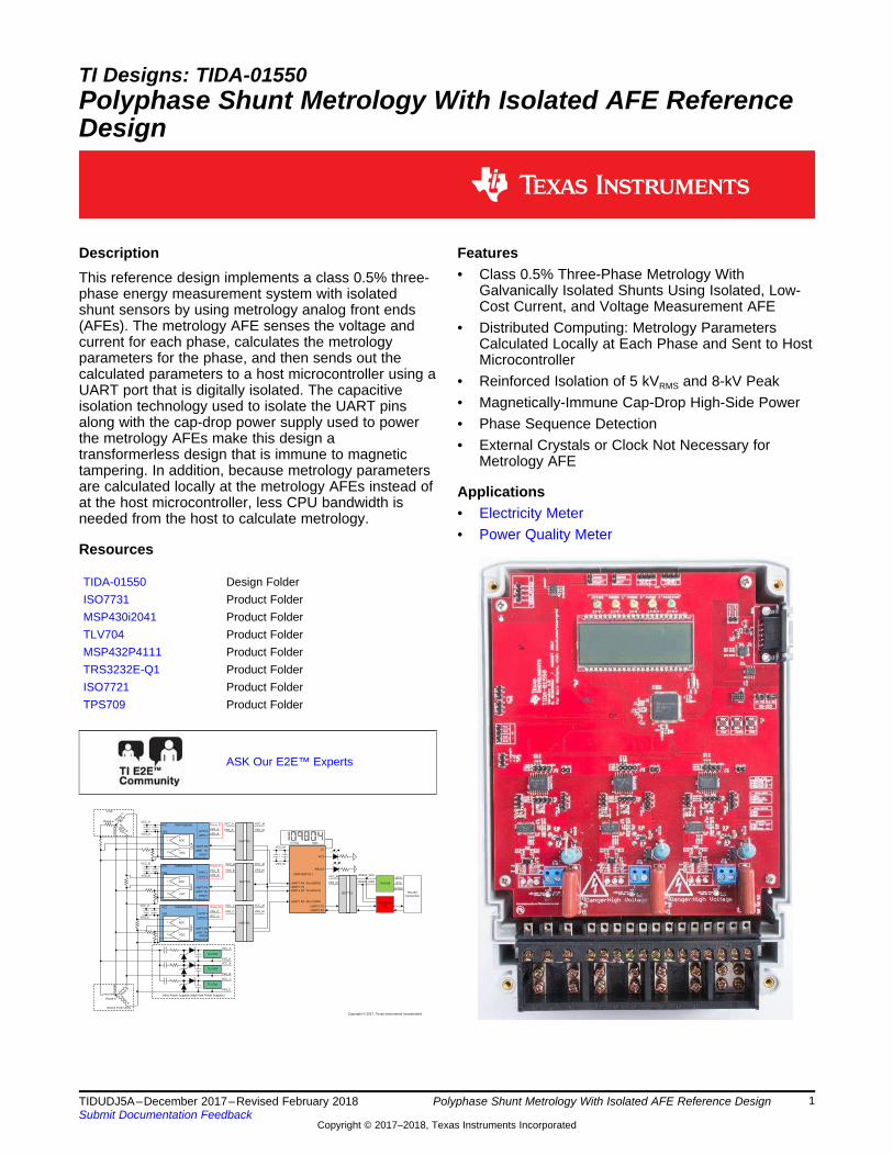
DescriptionThis reference design implements a class 0.5% three-phase energy measurement system with isolatedshunt sensors by using metrology analog front ends(AFEs). The metrology AFE senses the voltage andcurrent for each phase, calculates the metrologyparameters for the phase, and then sends out thecalculated parameters to a host microcontroller using aUART port that is digitally isolated. The capacitiveisolation technology used to isolate the UART pinsalong with the cap-drop power supply used to powerthe metrology AFEs make this design atransformerless design that is immune to magnetictampering. In addition, because metrology parametersare calculated locally at the metrology AFEs instead ofat the host microcontroller, less CPU bandwidth isneeded from the host to calculate metrology.
Resources
TIDA-01550 Design FolderISO7731 Product FolderMSP430i2041 Product FolderTLV704 Product FolderMSP432P4111 Product FolderTRS3232E-Q1 Product FolderISO7721 Product FolderTPS709 Product Folder
ASK Our E2E™ Experts
Features• Class 0.5% Three-Phase Metrology With
Galvanically Isolated Shunts Using Isolated, Low-Cost Current, and Voltage Measurement AFE
• Distributed Computing: Metrology ParametersCalculated Locally at Each Phase and Sent to HostMicrocontroller
• Reinforced Isolation of 5 kVRMS and 8-kV Peak• Magnetically-Immune Cap-Drop High-Side Power• Phase Sequence Detection• External Crystals or Clock Not Necessary for
Metrology AFE
Applications• Electricity Meter• Power Quality Meter

System Description www.ti.com
2 TIDUDJ5A–December 2017–Revised February 2018Submit Documentation Feedback
Copyright © 2017–2018, Texas Instruments Incorporated
Polyphase Shunt Metrology With Isolated AFE Reference Design
An IMPORTANT NOTICE at the end of this TI reference design addresses authorized use, intellectual property matters and otherimportant disclaimers and information.
1 System DescriptionThree-phase electricity meters measure the energy consumption at a business or industrial site. Toproperly sense energy consumption, voltage and current sensors translate mains voltage and current to avoltage range that an analog-to-digital converter (ADC) can sense. For three-phase electricity meters, it isnecessary for the current sensors to be isolated so they can properly sense the energy consumption ofmultiple phases without damaging the ADC. As a result, current transformers, which inherently haveisolation, have historically been used for the current sensors for three-phase electricity meters. Onedisadvantage of current transformers (and many transformers in general) is that they can be paralyzed byapplying a strong enough magnetic field so that the sensed energy consumption would be less than theactual energy consumption. Due to this weakness of current transformers against magnetic fields, it iscommon for people to try to tamper with a meter by placing a strong magnet outside the electricity meterto try to paralyze the current transformers to steal electricity. This reference design prevents magnettampering by using isolated shunts as current sensors instead of current transformers.
This reference design implements a class 0.5 three-phase energy measurement system with isolatedshunt sensors by using programmable metrology analog front-end (AFE) microcontrollers. The metrologyAFEs sense the voltage and current for each phase, calculates the metrology parameters for the phase,and then sends out the calculated parameters to a host microcontroller using a UART port. The keyparameters calculated by the metrology AFE include:• RMS current and voltage• Active power, reactive power, and apparent power factor• Frequency• Number of sag and swell occurrences• Total number of sag and swell cycles
External digital isolators capacitively isolate the UART communication between the host microcontrollerand the metrology AFE, which allows the host microcontroller to communicate to different metrology AFEsthat are referenced with respect to different phases. Because the metrology AFEs measure both voltageand current and have their UART pins externally isolated, voltage sensing is isolated in addition to therequired current sensing isolation necessary for implementing shunts in poly-phase systems. As a result,the host microcontroller is completely isolated from mains voltage. Also, because metrology parametersare calculated locally at the metrology AFEs instead of at the host microcontroller, less CPU bandwidth isneeded from the host to calculate metrology parameters.
In this reference design, the host microcontroller determines phase sequence, drives the board's liquidcrystal display (LCD), and communicates to a PC GUI through the board's isolated RS-232 circuitry. Thehost microcontroller also takes the metrology readings from the different metrology AFEs and aggregatesthese results. In addition, the host microcontroller accumulates the average active power readings sent bythe metrology AFEs to calculate the total consumed active energy. Using the host microcontroller toaccumulate the energy readings instead of the metrology AFEs enables the use of the metrology AFE'sinternal clock to calculate metrology parameters for many applications. Using the internal clock of themetrology AFE eliminates the need for external crystals or clocks for each metrology AFE, therebyreducing system cost. By having the metrology AFEs run off their own clock instead of feeding a clockthrough the isolation boundary, the data rate of the signals sent through the isolation boundary are greatlyreduced because only the actual metrology parameter values, which have a relatively low data rate, needto be sent to the host microcontroller. This low data rate reduces the current consumption of the digitalisolators as well as reduces emissions.
Each metrology AFE is powered by a cap-drop supply that is also transformerless. Because a transformeris not used in this reference design (whether a power supply transformer or current transformer), thisdesign is inherently magnetically immune, thereby preventing electricity theft due to magnetic tampering.Moreover, the high-side cap-drop power supply reduces the entire system cost, has inherent lowconducted and radiated emissions, and reduces the current consumption drawn from the low-side powersupply because the high-side is separately powered from mains instead of being derived from the low-sidepower supply.

www.ti.com System Description
3TIDUDJ5A–December 2017–Revised February 2018Submit Documentation Feedback
Copyright © 2017–2018, Texas Instruments Incorporated
Polyphase Shunt Metrology With Isolated AFE Reference Design
Another advantage of using shunts is that it does not share the same degradation in metrology results thatcurrent transformers show when harmonics are present in a system. As a result, these isolated shuntcurrent sensors can also be used for equipment that performs harmonic analysis such as power qualitymeters.
1.1 Key System Specifications
Table 1. Key System Specifications
PARAMETER SPECIFICATIONS DETAILSNumber of phases Three Section 2.1Accuracy class Class 0.5 Section 3.2.3Current sensor Shunt Section 2.3.1.3Voltage ADC type Sigma delta (integrated within MSP430i2041 metrology AFE) Section 2.3.1.3Sigma delta modulator clock 1,024,000 Hz Section 2.3.2.1.2Sigma delta oversampling ratio (OSR) 256 Section 2.3.2.1.2Ratio of skipped samples to total samples 0/5 Section 2.3.2.1.2Effective sample rate 4000 samples per second Section 2.3.2.1.2Phase compensation implementation Hardware (sigma delta module feature) Section 2.3.2.3.2Metrology AFE clock speed 16.384 MHz Section 2.3.2.1.1System nominal frequency 50 Hz Section 2.3.2.3.1
Measured parameters (updated every 50cycles)
Active power, reactive power, apparent power; root mean square(RMS) current and voltage; power factor; line frequency; sagand swell duration; sag and swell number of occurrences
Section 2.3.2.2.1
Isolation channels necessary Two or three Section 2.1Host MCU clock speed 48 MHz Section 2.3.2.1.4Utilized LEDs Total active energy and total reactive energy Section 2.3.2.4.3.2.1
Metrology AFE power Option 1: Power derived from mains using cap-drop supply;Option 2: External power Section 2.3.1.1
ADC
ADC-
Source From Utility
Load
Phase A Phase
C
Phase B
Phase APha
se B
Phase C
Neu
tral
+
+
-
VCC MSP430i2041
VSS
¯û
24
I
V
Neu
tral
UART RX
UART TX/
DRDY/PhaseSeq
ADC
ADC-
+
+
-
VCC MSP430i2041
VSS
¯û
24
I
V
UART RX
UART TX/
DRDY/PhaseSeq
ADC
ADC-
+
+
-
VCC MSP430i2041
VSS
I
V
UART RX
UART TX/DRDY/
PhaseSeq
+
-TOTAL
AB
kWh
UART2 TX
UART2 RX
GPIO
GPIO
GPIO
ISO7731
ISO7731
VCC_M
VSS_M
GPIO 1
GPIO 2
VSS_A
VSS_A
GPIO 1
GPIO 2
VCC_B
VSS_B
GPIO 1
GPIO 2
VSS_C
VCC_C
Phase ID
Phase ID
Phase ID
Lx
ACT
REACT
MSP432P4111
VCC_M
VSS_M
VCC_M
VSS_M
VCC_M
VSS_M
VCC_B
VSS_B
VCC_A
VSS_A
VCC_C
VSS_C
DTR
RTS
RGNDRS-232
ConnectionISO7721
VCC_M
VSS_M
RS232_VCC
RS232_GND
UART1 TXUART1 RX Pin A
UART1 RX Pin B
UART1 RX Pin C
TPS709
TRS3232E-Q1
ISO7731
¯û
24
i2041 Power Supplies(High Side Power Supplies)
VCC_A
VSS_A
VCC_B
VSS_B
VCC_C
VSS_C
TLV704
TLV704
TLV704
VCC_A
VSS_A
VCC_B
VSS_B
VCC_C
VSS_C
Copyright © 2017, Texas Instruments Incorporated
System Overview www.ti.com
4 TIDUDJ5A–December 2017–Revised February 2018Submit Documentation Feedback
Copyright © 2017–2018, Texas Instruments Incorporated
Polyphase Shunt Metrology With Isolated AFE Reference Design
2 System Overview
2.1 Block Diagram
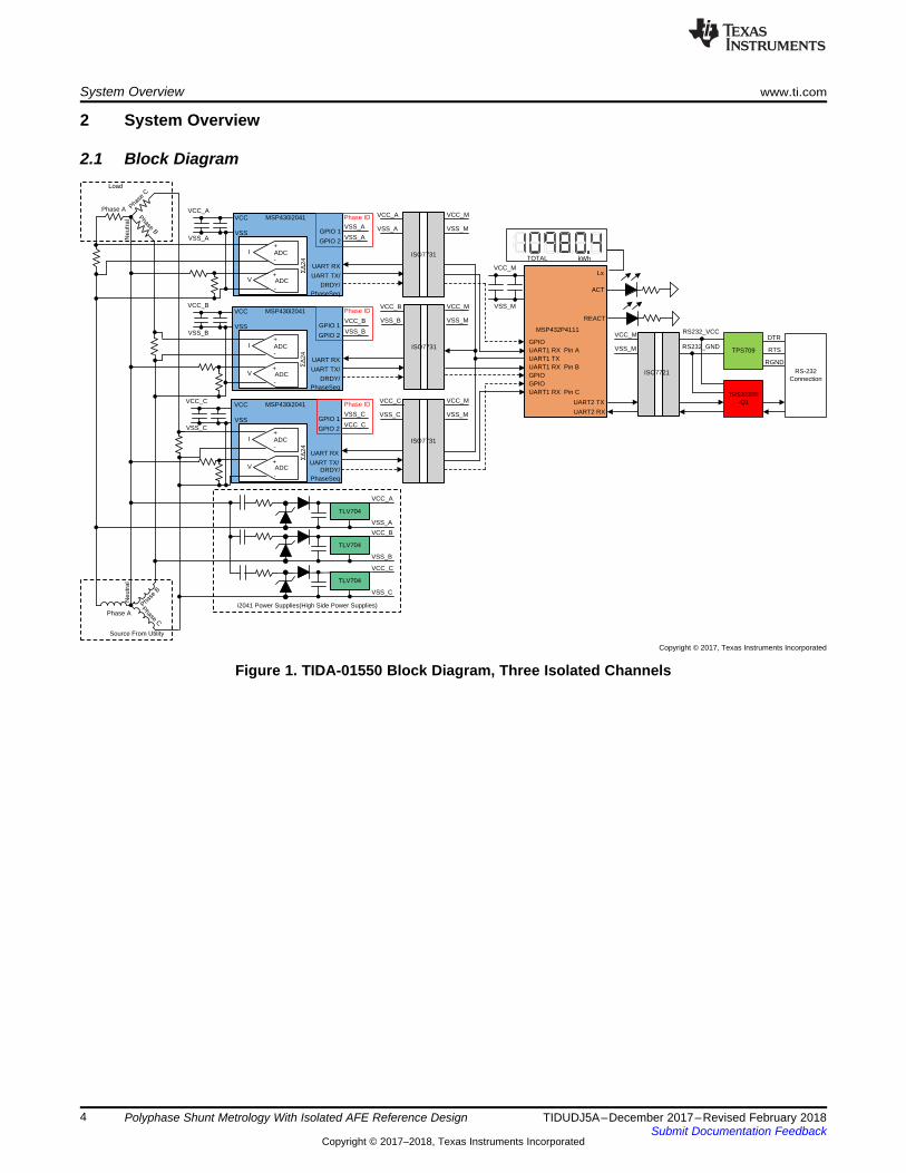
Figure 1. TIDA-01550 Block Diagram, Three Isolated Channels

ADC
ADC-
Source From Utility
Load
Phase A Phase
C
Phase B
Phase APha
se B
Phase C
Neu
tral
+
+
-
VCC MSP430i2041
VSS
¯û
24
I
V
Neu
tral
UART RX
UART TX/
DRDY/PhaseSeq
ADC
ADC-
+
+
-
VCC MSP430i2041
VSS
¯û
24
I
V
UART RX
UART TX/
DRDY/PhaseSeq
ADC
ADC-
+
+
-
VCC MSP430i2041
VSS
I
V
UART RX
UART TX/DRDY/
PhaseSeq
+
-TOTAL
AB
kWh
UART2 TX
UART2 RX
ISO7731
ISO7731
VCC_M
VSS_M
GPIO 1
GPIO 2
VSS_A
VSS_A
GPIO 1
GPIO 2
VCC_B
VSS_B
GPIO 1
GPIO 2
VSS_C
VCC_C
Phase ID
Phase ID
Phase ID
Lx
ACT
REACT
MSP432P4111
VCC_M
VSS_M
VCC_M
VSS_M
VCC_M
VSS_M
VCC_B
VSS_B
VCC_A
VSS_A
VCC_C
VSS_C
DTR
RTS
RGNDRS-232
ConnectionISO7721
VCC_M
VSS_M
RS232_VCC
RS232_GND
UART1 TXUART1 RX Pin A/GPIO
UART1 RX Pin B/GPIO
UART1 RX Pin C/GPIO
TPS709
TRS3232E-Q1
ISO7731
¯û
24
i2041 Power Supplies (High Side Power Supplies)
VCC_A
VSS_A
VCC_B
VSS_B
VCC_C
VSS_C
TLV704
TLV704
TLV704
VCC_A
VSS_A
VCC_B
VSS_B
VCC_C
VSS_C
Copyright © 2017, Texas Instruments Incorporated
www.ti.com System Overview
5TIDUDJ5A–December 2017–Revised February 2018Submit Documentation Feedback
Copyright © 2017–2018, Texas Instruments Incorporated
Polyphase Shunt Metrology With Isolated AFE Reference Design
Figure 2. TIDA-01550 Block Diagram, Two Isolated Channels
Figure 1 and Figure 2 depict a block diagram that shows the high-level interface used for a MSP430i20xxthree-phase energy measurement application with isolated shunts. These figures show a three-phase,four-wire star connection to the AC mains. In this reference design, each phase has a shunt currentsensor and a MSP430i20xx device. The MSP430i20xx device in this design is responsible for sensing themains voltage, sensing the current by measuring the voltage drop across the shunt, calculating themetrology parameters (except energy), and sending it to the MSP432™ host microcontroller in this design.The resistance of the shunt is selected based on the current range required for energy measurements andalso the minimization of the maximum power dissipation of the shunt. The MSP430i20xx senses the mainsvoltage by using resistor dividers as the voltage sensor to ensure that the input voltage to the ADC fitswithin the ADC's input voltage range. Because the MSP430i20xx can accept negative voltages, levelshifting the voltage from the resistor divider is not necessary. In this reference design, the superset four-channel MSP430i2041 device variant is used; however, to minimize cost, the two-channel MSP430i2020variant can also be used. To measure temperature in addition to voltage and current, the three-channelMSP430i2030 device can be used instead.
Only one UART module on the MSP432 communicates with the three MSP430i2041 devices. Multiplexingone MSP432's UART module to communicate with the different MSP430i2041 devices is done by usingan addressing scheme where the MSP432 provides the address of the MSP430i2041 device that it istalking to in the commands that the MSP432 sends. Whenever a command is sent by the MSP432 device,the MSP432 MCU sends it to all the MSP430i2041 devices, but only the addressed MSP430i2041 deviceresponds. The address of the different MSP430i2041 devices is configured by providing the propercombination of voltages (VSS or VCC) on two designated phase identification GPIO pins of theMSP430i2041 devices. Each device would have its own combination of voltages to ensure that eachdevice has a unique Phase ID. Using the phase identification addressing scheme allows the differentMSP430i2041 devices to communicate with the same MSP432 UART module without feeding in anyexternal chip select lines either through the isolation boundary or to the isolator output enable pins. Inaddition, the phase identification addressing scheme allows the same firmware to be programmed ontothe MSP430i2041 devices at the same time, thereby reducing programming time.

System Overview www.ti.com
6 TIDUDJ5A–December 2017–Revised February 2018Submit Documentation Feedback
Copyright © 2017–2018, Texas Instruments Incorporated
Polyphase Shunt Metrology With Isolated AFE Reference Design
Each MSP430i2041 device updates its metrology readings after 50 mains cycles of data has beenreceived. After new metrology readings have been received, a normally high data ready (DRDY) GPIO pinon the MSP430i2041 is asserted low to alert the MSP432 that new metrology parameters are ready.Because this GPIO pin assertion is done a fixed amount of time after the last zero crossing, the phasesequence can be detected by the MSP432 when the MSP430i2041 devices are synchronized byobserving the order at which this GPIO pins are asserted. To synchronize the different MSP430i2041devices, a sync command can be sent by the MSP432 device to make sure that the assertion of thedifferent MSP430i2041 DRDY GPIO pins are synchronized from the same starting point. In this referencedesign, there is an option to have the DRDY functionality implemented on a dedicated pin as shown inFigure 1 or to have it multiplexed with the UART TX pin as shown in Figure 2. The two-channelconfiguration is only valid when the shared UART TX/DRDY pin on the MSP430i2041 is connected to aGPIO pin on the host microcontroller that has the ability to dynamically switch between being a UART RXpin to being an interruptible GPIO input pin. For two-channel mode, the pins on the host microcontrollerthat are connected to the DRDY pins of the different MSP430i2041 devices must also be able to beconfigured as the same UART module port through the use of port mapping.
Because each MSP430i2041 device is referenced with respect to a different phase, it is necessary toisolate the communication from the MSP430i2041 to the MSP432. In this design, this isolation is done bythe ISO7731 devices; however, for the two channel configuration shown in Figure 2 , an ISO7721 devicecan be used instead to reduce cost. The low power consumption of these isolators enable power supplieswith limited maximum current specifications such as cap-drop supplies to be used to power each phase.For proper operation of the isolators, the output channels of different isolators must not be connected toeach other; however, the input channels can be directly connected to each other. As a result, althoughonly one UART module is used, the isolated UART TX signal output from the different MSP430i2041devices must not be physically connected to each other and fed into one RX pin for the MSP432 MCU.Instead of physically connecting together the different isolated UART TX signals from the MSP430i2041devices, in this design each of these signals is fed into a different port mappable GPIO pin that has theability to be configured as the RX functionality of the same UART module. An alternative approach, whichis not used in this reference design, is to connect the different isolated UART TX signals to inputs of anOR/AND logic gate and to connect the output of this logic gate to one UART RX pin of the MSP432 MCU.
To power the MSP430i2041 devices and the high-side of the isolators, each phase has an external powersupply. Because each MSP430i2041 and the high-side of its corresponding isolator must be referencedfrom a different line voltage, three different cap-drop supplies are used. Each implemented power supplyprovides power to the associated MSP430i2041 and isolator by using a half-bridge cap-drop power supplybetween the line of that phase and neutral.
This reference design uses the MSP432P4111 as the host microcontroller. The MSP432P4111aggregates the data from the different MSP430i2041 devices. The MSP432P4111 also accumulates thepower readings into energy, which allows the MSP430i2031 device to use its own internal clock so thatexternal clock components such as clock generators are not necessary. The MSP432 MCU is responsiblefor outputting the active and reactive energy pulses used for accuracy measurement and calibration. Inaddition to isolated pulses, the design also supports isolated RS-232 communication through the use ofthe TPS70933, ISO7721, and TRS3232E-Q1 devices. For more information on the isolated RS-232portion of the design, see the Self-Powered Isolated RS-232 to UART Interface Reference Design.
2.2 Highlighted Products
2.2.1 ISO7731
The ISO7731 device is a high-performance, triple-channel digital isolator with 5000-VRMS (DW package)and 3000-VRMS (DBQ package) isolation ratings per UL 1577. The ISO7731 device provides highelectromagnetic immunity and low emissions at low power consumption, while isolating CMOS orLVCMOS digital I/Os. Each isolation channel has a logic input and output buffer separated by a silicondioxide (SiO2) insulation barrier. This device comes with enable pins that can be used to put the respectiveoutputs in high impedance for multi-master driving applications and to reduce power consumption.Through innovative chip design and layout techniques, the electromagnetic compatibility of the ISO7731device has been significantly enhanced to ease system-level ESD, EFT, surge, and emissionscompliance.

ClockSystem Flash
32KB16KB
MCLK
ACLK
SMCLK
16.384-MHzCPU
with 16registers
Emulation2BP
JTAGInterface
WatchdogWDT
15 or 16 bit
SD24
3Sigma-DeltaAnalog-to-
DigitalConverters
TA0
Timer_A3 CC
Registers
RAM
2KB1KB
PowerManagement
LDOREF
VMONBrownout
Spy-Bi-Wire
HardwareMultiplier(16x16)
MPY,MPYS,MAC,MACS
Port P1
8 I/Os,Interruptcapability
MAB
MDB
eUSCI_A0
UART,IrDA, SPI
eUSCI_B0
SPI, I C2
Port P2
8 I/Os,Interruptcapability
TA1
Timer_A3 CC
Registers
ROSC VCC DVSS AVSS VCORE RST/NMI P1.x
8
P2.x
8
Copyright © 2018 Texas Instruments Incorporated
www.ti.com System Overview
7TIDUDJ5A–December 2017–Revised February 2018Submit Documentation Feedback
Copyright © 2017–2018, Texas Instruments Incorporated
Polyphase Shunt Metrology With Isolated AFE Reference Design
2.2.2 MSP430i2041The MSP430i2041 metrology AFE device finds its application in power and energy measurement and hasthe necessary architecture to support it. The MSP430i2041 device1 has an internal 16.384-MHz DCO,which generates system clocks without an external crystal. The MSP430i2041 has four independent, 24-bit, ΣΔ ADCs based on a second-order sigma-delta architecture that supports differential inputs. Thesigma-delta module (referred to as SD24) operate independently, are capable of 24-bit results, and can begrouped together for simultaneous sampling of voltages and currents on the same trigger. In addition,each converter also has an integrated gain stage for amplification of low-output current sensors. TheMSP430i2041 device also has a 16-bit × 16-bit hardware multiplier that can be used to further acceleratemath intensive operations during metrology computations. Figure 3 shows these features as well asadditional ones for the MSP430i2041 metrology AFE. The key parameters calculated duringmeasurements by the MSP430i2041 are as follows:• RMS current and voltage• Active and reactive power• Power factor• Frequency• Sag duration• Number of sag occurrences• Swell duration• Number of swell occurrences
Figure 3. Functional Block Diagram of MSP430i2041
System Overview www.ti.com
8 TIDUDJ5A–December 2017–Revised February 2018Submit Documentation Feedback
Copyright © 2017–2018, Texas Instruments Incorporated
Polyphase Shunt Metrology With Isolated AFE Reference Design
2.2.3 TLV704The TLV70433 low-dropout (LDO) regulator is an ultra-low quiescent current devices designed forextremely power-sensitive applications. Quiescent current is virtually constant over the complete loadcurrent and ambient temperature range. These devices are an ideal power-management attachment tolow-power microcontrollers such as the MSP430™. The TLV70433 operates over a wide operating inputvoltage of 2.5 V to 24 V. Thus, the device is an excellent choice for both battery-powered systems as wellas industrial applications that undergo large line transients.
2.2.4 MSP432P4111The SimpleLink™ MSP432P4111 MCUs are optimized MCUs that deliver ultra-low-power performancewith FPU and DSP extensions. This device has an Arm® 32-Bit Cortex®-M4F CPU with Floating-Point Unitand Memory Protection Unit, a real-time clock, LCD driver, port mappable GPIOs, an AES encryption anddecryption accelerator, and multiple serial communication options. The MSP432P4111 device is part ofthe SimpleLink MCU platform, which consists of Wi-Fi®, Bluetooth® low energy, Sub-1 GHz, and hostMCUs. All of these devices share a common, easy-to-use development environment with a single-coresoftware development kit (SDK) and rich tool set.
2.2.5 TRS3232E-Q1To properly interface with the RS-232 standard, a voltage translation system is required to convertbetween the 3.3-V domain on the board and from the 12 V on the port itself. To facilitate the translation,the design uses a TRS3232E-Q1 device. The TRS3232E-Q1 device is capable of driving the highervoltage signals on the RS-232 port from only the 3.3-V DVCC through a charge pump system.
The TRS3232E-Q1 device consists of two line drivers, two line receivers, and a dual charge-pump circuitwith ±15-kV electrostatic discharge (ESD) protection pin-to-pin (serial-port connection pins, includingGND). The device meets the requirements of the Telecommunications Industry Association and ElectronicIndustries Alliance TIA/EIA-232-F and provides the electrical interface between an asynchronouscommunication controller and the serial-port connector. The charge pump and four small externalcapacitors allow operation from a single 3-V to 5.5-V supply. The devices operate at data signaling ratesup to 250 kbit/s and a maximum of 30-V/µs driver output slew rate.
2.2.6 ISO7721
To add isolation to the RS-232 connection to a PC, the isolated RS-232 portion of this reference designuses capacitive galvanic isolation, which has an inherent lifespan advantage over an opto-isolator. Inparticular, industrial devices are usually pressed into service for much longer periods of time thanconsumer electronics; therefore, maintenance of effective isolation over a period of 15 years or longer isimportant.
The variant of the ISO7721 used in the RS-232 circuitry of this reference design provides galvanicisolation up to 3.0 kVRMS for one minute per UL. This digital isolator has two isolated channels where oneis a forward channel and the other is a reverse channel. Each isolation channel has a logic input andoutput buffer separated by a silicon dioxide (SiO2) insulation barrier. This chip supports a signaling rate of100 Mbps. The chips can operate from a 3.3-V and 5-V supply and logic levels.
2.2.7 TPS709To power the data terminal equipment (DTE) side of the isolation boundary and the RS-232 charge pump,there are two choices. The interface can either implement an isolated power supply or harvest power fromthe RS-232 line. Integrating a power supply adds cost and complexity to the system, which is difficult tojustify in low-cost sensing applications.
To implement the second option of harvesting power from the RS-232 port itself, this reference designuses the flow control lines that are ignored in most embedded applications. The RS-232 specification(when properly implemented on a host computer or adapter cable), keeps the request to send (RTS) anddata terminal ready (DTR) lines high when the port is active. As long as the host has the COM port open,these two lines retain voltage on them. This voltage can vary from 5 V to 12 V, depending on the driverimplementation. The 5 V to 12 V is sufficient for the use requirements in this design.

Copyright © 2017, Texas Instruments Incorporated
www.ti.com System Overview
9TIDUDJ5A–December 2017–Revised February 2018Submit Documentation Feedback
Copyright © 2017–2018, Texas Instruments Incorporated
Polyphase Shunt Metrology With Isolated AFE Reference Design
The voltage is put through a diode arrangement to block signals from entering back into the pins. Thevoltage charges a capacitor to store energy. The capacitor releases this energy when the barrier andcharge pump pull more current than what is instantaneously allowed. The TPS70933 is used to bring theline voltage down to a working voltage for the charge pump and isolation device.
The TPS70933 linear regulator is an ultra-low quiescent current devices designed for power-sensitiveapplications. A precision band-gap and error amplifier provides 2% accuracy over temperature. Aquiescent current of only 1 µA makes these devices ideal solutions for battery-powered, always-onsystems that require very little idle-state power dissipation. These devices have thermal-shutdown,current-limit, and reverse-current protections for added safety. These regulators can be put into shutdownmode by pulling the EN pin low. The shutdown current in this mode goes down to 150 nA (typical).
2.3 System Design Theory
2.3.1 Design Hardware Implementation
2.3.1.1 High-Side Power SupplyTo properly sense, calculate, and send metrology parameters, it is necessary for the MSP430i2041 andthe high-side of the corresponding isolation device to be powered. Because each MSP430i2041 deviceand corresponding isolator are referenced from a different line voltage, a different high-side power supplyis required for each power supply. In this reference design, there are two high-side power supply options:an onboard half-bridge cap-drop power supply or an off-board, custom power supply.
There are multiple advantages to using the onboard cap-drop high-side power supply. First, this cap-droppower supply does not have any magnetic components, so the power supply would be magneticallyimmune to magnetic fields instead of only being magnetically tolerant to a certain limit. Additionally, cap-drop supplies are relatively inexpensive compared to alternative power supply options. Also, LDO-basedcap-drop power supplies inherently have low conducted and radiated emissions compared to SMPSpower supplies. Finally, because the high-side power is derived directly from mains instead of from thehost MCU's power supply, less current is drawn from the host MCU's power supply, thereby allowing thespecifications on that power supply's maximum current drive to be relaxed.
Figure 4 shows the design's implementation of the high-side power supply. In this implementation, aTLV70433-based, half-bridge, cap-drop power supply translates the mains voltage to the necessary 3.3 Vneeded to power the MSP430i2041 and the high-side of the ISO7731. As an alternative to using theonboard cap-drop power supply, the design has the option to instead power the MSP430i2041 andISO7731 by providing the necessary 3.3 V from an external isolated voltage supply to the associatedterminal block (U$13 in Figure 4).
Figure 4. High-Side Power Supply
Cap-drop power supplies have a limited maximum current so it is important that their load be low-power.Table 2 shows a typical current consumption of 4.5 mA when the MSP430i2041 device is running in activemode at 16.384 MHz. Based on Table 3, there is also a maximum additional current consumption of 250µA per ADC converter turned on, resulting in an additional 500 µA of current drawn from the power supplyto properly sense voltage and current.

System Overview www.ti.com
10 TIDUDJ5A–December 2017–Revised February 2018Submit Documentation Feedback
Copyright © 2017–2018, Texas Instruments Incorporated
Polyphase Shunt Metrology With Isolated AFE Reference Design
(1) Over recommended ranges of supply voltage and operating free-air temperature (unless otherwise noted)(2) All inputs are tied to 0 V or VCC. Outputs do not source or sink any current.(3) All peripherals are inactive.
Table 2. MSP430i2041 Active Mode Current Consumption (1) (2) (3)
PARAMETER TEST CONDITIONS VCC MIN TYP MAX UNIT
IAM, 1.024MHz
Active modecurrent at1.024 MHz
fDCO = 16.384 MHz, fMCLK = fSMCLK = 1.024 MHz,fACLK = 32 kHz,Program executes from flash,CPUOFF = 0, SCG0 = 0, SCG1 = 0, OSCOFF = 0
3 V 1.6 mA
IAM, 8.192MHz
Active modecurrent at8.192 MHz
fDCO = 16.384 MHz, fMCLK = fSMCLK = 8.192 MHz,fACLK = 32 kHz,Program executes from flash,CPUOFF = 0, SCG0 = 0, SCG1 = 0, OSCOFF = 0
3 V 3.0 mA
IAM, 16.384MHz
Active modecurrent at16.384 MHz
fDCO = fMCLK = fSMCLK = 16.384 MHz,fACLK = 32 kHz,Program executes from flash,CPUOFF = 0, SCG0 = 0, SCG1 = 0, OSCOFF = 0
3 V 4.5 mA
Table 3. MSP430i2041 SD24 Current Consumption
PARAMETER TEST CONDITIONS VCC MIN TYP MAX UNITVCC Supply voltage range AVSS = DVSS = 0 V 2.2 3.6 V
ISD24
Analog plus digital supply current perconverter (reference current notincluded)
SD24OSRx =256
GAIN: 1, 2, 4, 8, 16 3 V 190µA
GAIN: 1, 16 3 V 250
This reference design uses a baud rate of 57600 baud. The current consumption of the isolatorsdecreases as frequency decreases, which indicates that the maximum current consumption of theISO7731 is less than the 3.4-mA maximum current consumption at 1 Mbps mentioned in Figure 5. Thecap-drop in this implementation is designed to provide more than the 8.4 mA needed to power theMSP430i2041 core, the MSP430i2041 converters, and the digital isolators.
Figure 5. ISO7731 Current Consumption
2.3.1.2 External Resistor and Oscillator For Metrology AFE ClockThe MSP430i2041 internal DCO supports two modes of operation. This device can operate with aninternal resistor or an external resistor that is connected to ROSC pin of the device. The internal resistoroption is the lowest cost option because it does not require any external components while the externalresistor option provides the most accurate clock. When selecting the external resistor option, arecommended 20-kΩ, ±50-ppm resistor with 0.1% tolerance is recommended. This resistor is populatedon this reference design in case it is desired to use external resistor mode for other applications; however,the software is configured by default not to use this external resistor option because the energy

1N4148
1N4148
1K
1K
47pF
47pF
15nF
DNP
SM
AJ5
.0CA 0
0
DN
PD
NP
DN
PD
NP
D26
D27
D28
D29
R33
R34
I1+
I1-
C78
C79
C80
R14
I1G
ND
TVS2
R/L1
R/L2
AFE1_GND
AFE1_GNDAFE1_GND
AFE1_VCC
AFE1_VCC
AFE1_I+
AFE1_I-
Copyright © 2017, Texas Instruments Incorporated
330k 330k 330k
1K
100
2.7
k
47pF
47pF
15nF
S20K275
0
0
R29 R30 R42
R43
R45
R46
C58
C59
C77
NLIN
E1
R2
R/L3
R/L4
AFE1_V+
AFE1_V-
AFE1_GND
AFE1_GND
NEU
TRAL
Copyright © 2017, Texas Instruments Incorporated
www.ti.com System Overview
11TIDUDJ5A–December 2017–Revised February 2018Submit Documentation Feedback
Copyright © 2017–2018, Texas Instruments Incorporated
Polyphase Shunt Metrology With Isolated AFE Reference Design
accumulation from power is done by the MSP432 host MCU and using the internal resistor option is thelowest cost option. For applications that require an accurate clock for precise measurement of other timedependent calculations besides energy (such as line frequency), the external resistor option can be usedby modifying the metrology AFE firmware to select the external resistor option instead of the internalresistor option.
2.3.1.3 Analog InputsThe MSP430i2041’s AFE circuitry, which consists of the ΣΔ ADC within the MSP430i2041's SD24 module,is differential and requires that the input voltages at the pins do not exceed ±928 mV when a gain of 1 isused and ±58 mV when a gain of 16 is used. To meet this specification, the current and voltage inputsneed to be scaled down. In addition, the SD24 ADCs allows a maximum negative voltage of –1 V.Therefore, the AC current signal from mains can be directly interfaced without the need for level shifters.This section describes the AFE circuitry used for the voltage and current channels.
2.3.1.3.1 Voltage Front End CircuitryThe voltage from the mains is usually 230 V or 120 V and must be scaled down within 928 mV. The AFEcircuitry for voltage consists of spike protection varistors followed by a voltage divider network, and a RClow-pass filter that acts like an antialiasing filter. For this design, footprints for suppressant inductors arealso available. These inductor footprints are shown in Figure 6 as R/L3 and R/L4, and by default arepopulated with 0-Ω resistors.
Figure 6. MSP430i2041 Voltage Front-End Circuitry
Figure 6 shows the AFE circuitry for the voltage inputs for a mains voltage of 230 V. In this circuitry, thevoltage is brought down to approximately 626-mV RMS, which is a 885-mV peak, and fed to the positiveinput of the convertor. The antialiasing resistors on the positive and negative sides are different becausethe input impedance to the positive terminal is much higher; therefore, a lower value resistor is used forthe antialiasing filter. If this is not maintained, a relatively large phase shift appears between voltage andcurrent samples.
2.3.1.3.2 Current Front-End CircuitryThe AFE circuitry for current inputs is slightly different from the AFE circuitry for the voltage inputs.Figure 7 shows the AFE circuitry used for a current channel.
Figure 7. MSP430i2041 Current Front-End Circuitry
The AFE circuitry for current consists of diodes and transorbs for any additional transient voltagesuppression, footprints (R/L1 and R/L2) that could be replaced with inductors for EMI suppression (thesefootprints are populated with 0-Ω resistors by default), and an antialiasing filter.

System Overview www.ti.com
12 TIDUDJ5A–December 2017–Revised February 2018Submit Documentation Feedback
Copyright © 2017–2018, Texas Instruments Incorporated
Polyphase Shunt Metrology With Isolated AFE Reference Design
Figure 7 shows the three-terminal shunt used for current measurement to be connected at I1+, I1−, andI1GND. The value of this shunt is selected based on balancing maximizing the peak analog voltage inputinto the MSP430i2041 with minimizing the power dissipation of the shunt. In particular, for optimalaccuracy, the peak DC voltage fed into the MSP430i2041 must be as close as possible to 58 mV withoutsurpassing this voltage. This peak voltage is dependent on the rated maximum current of the system andthe resistance of the selected shunt. For example, this reference design uses 400-µΩ shunts (for moreinformation on the shunts used, see http://www.vishay.com/docs/30173/wsms3124.pdf). With these 400-µΩ shunts and a maximum RMS current of 90 A, the maximum DC voltage fed into the MSP430i2041SD24 ADC is 90 × √2 × (400 × 10–6) = 51 mV. To minimize the power dissipation in the shunt, a smallervalue shunt can also be used. This reference design also uses 220-µΩ shunts; however, by using smallervalue shunts, the voltage fed into the MSP430i2041 ADC is also reduced. As a result, there is a tradeoff inaccuracy. Based on the requirements of the system, the tradeoff in accuracy from using a shunt with asmall resistance and the reduced power dissipation from choosing the smaller shunt must be taken intoaccount when selecting the proper shunt value.
2.3.2 Design Software ImplementationThis section discusses the software for this reference design. Section 2.3.2.1 discusses the setup ofvarious peripherals of the metrology and host processors. Section 2.3.2.2 and Section 2.3.2.3 describe themetrology software as two major processes: the foreground process and background process.Section 2.3.2.4 describes the application software. Section 2.3.2.5 describes the MSP430i2041 toMSP432 communication process.
2.3.2.1 Peripheral Setup
2.3.2.1.1 MSP430i2041 Start-up CodeThe INFO memory of each MSP430i2041 device stores device-specific calibration values. These valuesaffect items such as clock accuracy, SD24 operation, and reference voltage operation. For properfunctionality of this device, these values need to be loaded into the proper calibration and trim registers, asmentioned in the TLV and Start-Up Code section of the MSP430i2xx Family User's Guide . In addition, adecision whether to secure or unsecure the MSP430i2041 must be made in the first 64 MCLK cycles afterRESET. Both of these functions are accomplished in the low_level_init function (in low_level_init.c), whichruns before even the main function is called.
Because the device-specific peripheral calibration is stored in INFO memory, do not change the projectsettings to erase INFO memory as that erases these values. Also note that meter calibration data is storedin the same segment as the peripheral calibration information. As a result, do not delete the peripheralcalibration values if performing meter calibration. This reference design stores the device-specificperipheral calibration data before erasing the INFO memory, and then rewrites INFO memory with thisperipheral calibration factors as well as any new meter accuracy calibration factors.
2.3.2.1.2 MSP430i2041 SD24 SetupThe MSP430i2041 has four sigma-delta data converters, which are used to measure the voltage andcurrents in the system. This reference design only uses two of the four sigma-delta converters. For theMSP430i2041, the clock to the SD24 ADCs (fM) is fixed at 1.024000 MHz. In the software, an OSR of 256is chosen, which results in a sampling frequency of 4.000 ksps for the converters. At every samplinginstance, the ADCs are configured to generate regular interrupts.
In the software, the following channel associations are used:• A0.0+ and A0.0- → Current• A1.0+ and A1.0- → Voltage
2.3.2.1.3 MSP430i2041 AFE UART SetupThe MSP430i2041 is configured to communicate to the MSP432P4111 using a UART module configuredfor 8N1 at 57,600 baud. When the device is configured in two-channel mode, the UART TX pin is switchedbetween UART TX functionality and DRDY GPIO functionality.
100K
100K
100K
75K
GND
R6
R7
R17
R18
DVCC
R23/P7.2
R13/P7.1
R03/P7.0
P7.3
Copyright © 2017, Texas Instruments Incorporated
www.ti.com System Overview
13TIDUDJ5A–December 2017–Revised February 2018Submit Documentation Feedback
Copyright © 2017–2018, Texas Instruments Incorporated
Polyphase Shunt Metrology With Isolated AFE Reference Design
2.3.2.1.4 MSP432P4111 Clock SetupThe MSP432 is configured to have its CPU clock (MCLK) set at 48 MHz and its subsystem master clock(SMCLK) set to 12 MHz. The clock source for MCLK and SMCLK is an external 48-MHz crystal. Anexternal 32.768-kHz crystal is used as the clock source for the device's auxiliary clock (ACLK). This ACLKclock is set to a frequency of 32.768 kHz. The clock is configured using MSP432 driverlib functions.
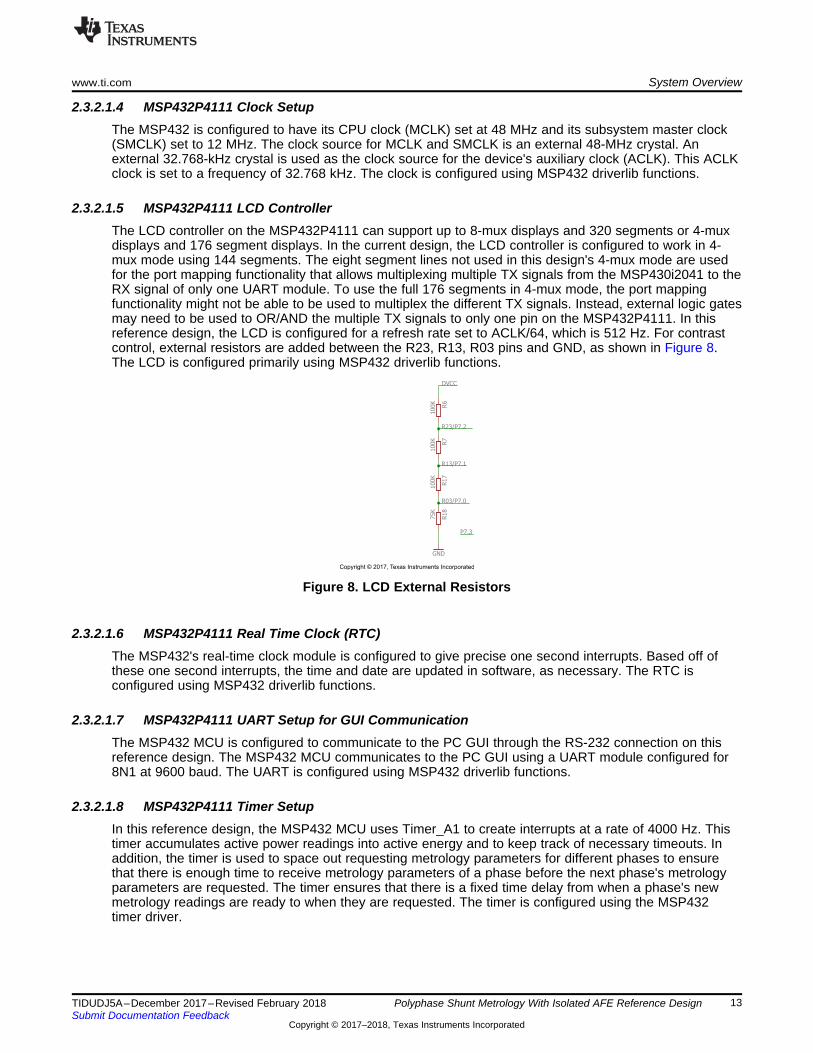
2.3.2.1.5 MSP432P4111 LCD ControllerThe LCD controller on the MSP432P4111 can support up to 8-mux displays and 320 segments or 4-muxdisplays and 176 segment displays. In the current design, the LCD controller is configured to work in 4-mux mode using 144 segments. The eight segment lines not used in this design's 4-mux mode are usedfor the port mapping functionality that allows multiplexing multiple TX signals from the MSP430i2041 to theRX signal of only one UART module. To use the full 176 segments in 4-mux mode, the port mappingfunctionality might not be able to be used to multiplex the different TX signals. Instead, external logic gatesmay need to be used to OR/AND the multiple TX signals to only one pin on the MSP432P4111. In thisreference design, the LCD is configured for a refresh rate set to ACLK/64, which is 512 Hz. For contrastcontrol, external resistors are added between the R23, R13, R03 pins and GND, as shown in Figure 8.The LCD is configured primarily using MSP432 driverlib functions.
Figure 8. LCD External Resistors
2.3.2.1.6 MSP432P4111 Real Time Clock (RTC)The MSP432's real-time clock module is configured to give precise one second interrupts. Based off ofthese one second interrupts, the time and date are updated in software, as necessary. The RTC isconfigured using MSP432 driverlib functions.
2.3.2.1.7 MSP432P4111 UART Setup for GUI CommunicationThe MSP432 MCU is configured to communicate to the PC GUI through the RS-232 connection on thisreference design. The MSP432 MCU communicates to the PC GUI using a UART module configured for8N1 at 9600 baud. The UART is configured using MSP432 driverlib functions.
2.3.2.1.8 MSP432P4111 Timer SetupIn this reference design, the MSP432 MCU uses Timer_A1 to create interrupts at a rate of 4000 Hz. Thistimer accumulates active power readings into active energy and to keep track of necessary timeouts. Inaddition, the timer is used to space out requesting metrology parameters for different phases to ensurethat there is enough time to receive metrology parameters of a phase before the next phase's metrologyparameters are requested. The timer ensures that there is a fixed time delay from when a phase's newmetrology readings are ready to when they are requested. The timer is configured using the MSP432timer driver.

System Overview www.ti.com
14 TIDUDJ5A–December 2017–Revised February 2018Submit Documentation Feedback
Copyright © 2017–2018, Texas Instruments Incorporated
Polyphase Shunt Metrology With Isolated AFE Reference Design
2.3.2.1.9 MSP432P4111 Port MappingThe MSP432 MCU has a port mapping controller that allows a flexible mapping of digital functions to portpins. The set of digital functions that can be ported to other pins is dependent on the device. For theMSP432 device in particular, the EUSCIA1 UART module's TX and RX functionality are available to portsP2, P3, and P7. In this reference design, this port mapping feature provides flexibility in the PCB layout aswell as multiplexing the three TX signals from the different MSP430i2041 devices to the RX signal of thesame EUSCIA1 UART port. In this reference design, the three different TX signals are connected todifferent port mappable GPIO pins. Each of these pins have their port mapping functionality changedswitched between "PMAP_NONE" functionality, which disables mapping a digital function to a particularpin, and "PMAP_UCA1RXD", which enables communication to a corresponding metrology AFE. Thedesign's software ensures that only one port mapping pin at a time is configured to PMAP_UCA1RXDfunctionality. Whenever the MSP432 device requests data from a particular metrology AFE, the MCUsends the command to all the metrology AFEs and enables only the PMAP_UCA1RXD functionality on theMSP432's port mapping GPIO pin that is connected to the desired MSP430i2041's UART TX pin.
When the host is configured for two-channel mode, the port mapping pins are also switched from portmapping functionality to interruptible GPIO pins. Because only the P2 and P3 ports of the MSP432 haveboth port mappable and interruptible GPIO input pins, this two-channel mode only works with ports P2 andP3 on the MSP432. In two-channel mode, the port mapping pins are configured as interruptible input pinsmajority of the time. The only time the port mapping pins are configured for the PMAP_UCA1RXDfunctionality is when the MSP432 has sent a command to a specific MSP430i2041 device and it isexpecting a response back. Once the requested data has been correctly received by the MSP432P4111or there has been a timeout, the corresponding port mapping pin is configured back to be an interruptibleGPIO pin.
Using the port mapping controller, the following mappings are used:• PMAP_UCA1TXD (EUSCIA1 UART TX) → Port P2.6• PMAP_UCA1RXD (EUSCIA1 UART RX) → Port P2.5 (Connected to the isolated UART Tx signal from
Phase A's MSP430i2041)• PMAP_UCA1RXD (EUSCIA1 UART RX) → Port P2.3 (Connected to the isolated UART Tx signal from
Phase B's MSP430i2041)• PMAP_UCA1RXD (EUSCIA1 UART RX) → Port P2.1 (Connected to the isolated UART Tx signal from
Phase C's MSP430i2041)
The port mapping functionality is configured using the driverlib; however, the majority of the other GPIOpins are configured using the MSP432 GPIO driver.

www.ti.com System Overview
15TIDUDJ5A–December 2017–Revised February 2018Submit Documentation Feedback
Copyright © 2017–2018, Texas Instruments Incorporated
Polyphase Shunt Metrology With Isolated AFE Reference Design
2.3.2.1.10 MSP432P4111 Direct Memory Access (DMA)The direct memory access (DMA) module transfers packets from the MSP430i2041 to the MSP432P4111with minimal bandwidth requirements from the MSP432's CPU. Only the third channel of the DMA is used.The DMA transfers each byte received from the MSP432's EUSCIA1 UART module's RX signal tomemory until an entire packet of data has been received. Once an entire packet of data has beenobtained, the DMA module triggers an interrupt to immediately parse any critical data.
2.3.2.1.11 MSP432P4111 Interrupt PrioritiesThe software has five interrupts that are priorities. Table 4 lists these interrupt priorities, with the smallerpriority codes having higher interrupt priorities.
Table 4. MSP432P4111 Interrupt Priorities
INTERRUPT SIGNIFICANCE PRIORITY CODETA1_0 Update energy accumulation registers and timeout state 0x20
PORT2 New metrology readings are now available for a particular MSP430i2041device 0x40
DMA1 Received response packet from a MSP430i2041 device 0x60
EUSCIA0 UART transmit buffer empty for sending a packet to the PC GUI or newUART character has been received from the PC GUI 0x80
RTC A new second has elapsed every time this interrupt is triggered. Everytwo seconds, update the LCD. 0x80

RESET
HW setup:Clock, SD24, Port pins, eUSCI
Calculate metrology readings
Notified by background process to calculate new readings?
Y
MSP432 frame reception management
N
HW setup:Clock, SD24, Port pins, eUSCI UART,
Phase identification update
Start Up Code
Alert MSP432 that new frame of data is ready by asserting DRDY
System Overview www.ti.com
16 TIDUDJ5A–December 2017–Revised February 2018Submit Documentation Feedback
Copyright © 2017–2018, Texas Instruments Incorporated
Polyphase Shunt Metrology With Isolated AFE Reference Design
2.3.2.2 MSP430i2041 Metrology Foreground ProcessThe foreground process includes the initial setup of the MSP430i2041 hardware and software immediatelyafter a device RESET. Figure 9 shows the flowchart for this process.
Figure 9. Metrology Foreground Process
The initialization routines involve the setup of the ADC, clock system, general purpose input/output (port)pins, phase identification (whether a particular device is set to be Phase A, Phase B, or Phase C), and theUSCI_A0 for UART functionality. After the hardware is set up, any received frames from theMSP432P4111 are processed. Subsequently, the foreground process checks whether the backgroundprocess has notified it to calculate new metering parameters. This notification is done through theassertion of the "PHASE_STATUS_NEW_LOG" status flag whenever a frame of data is available forprocessing. The data frame consists of the processed dot products that were accumulated for 50 cycles inthe background process.

Sample Count
90, ph phn 1
REACT, ph REACT, ph React _ Offset,ph
V (n) i (n)
P K PSample Count
u
¦
Sample Count
phn 1
ACT, ph ACT, ph ACT _ Offset,ph
v(n) i (n)
P K PSample Count
u
¦
www.ti.com System Overview
17TIDUDJ5A–December 2017–Revised February 2018Submit Documentation Feedback
Copyright © 2017–2018, Texas Instruments Incorporated
Polyphase Shunt Metrology With Isolated AFE Reference Design
The processed dot products include the VRMS, IRMS, active power, and reactive power. These dot productsare used by the foreground process to calculate the corresponding metrology readings in real world units.Processed voltage dot products are accumulated in 48-bit registers. In contrast, processed current dotproducts, active energy dot products, and reactive energy dot products are accumulated in separate 64-bitregisters to further process and obtain the RMS and mean values. Using the foreground's calculatedvalues of active and reactive power, the apparent power is calculated. The frequency (in Hertz) and powerfactor are also calculated using parameters calculated by the background process using the formulas inSection 2.3.2.2.1. Once new metrology readings have been calculated, the DRDY pin is asserted low for aduration of approximately 5 ms, thereby alerting the MSP432 MCU that new metrology parameters areready.
2.3.2.2.1 MSP430i2041 Metrology FormulasThis section briefly describes the formulas used for the voltage, current, and power calculations. Aspreviously described, voltage and current samples are obtained at a sampling rate of 4000 Hz. All of thesamples that are taken in 50 cycles are kept and used to obtain the RMS values for voltage and currentfor each phase. The RMS values are obtained by the following formulas:
(1)
(2)
where:• ph = Phase parameters that are being calculated [that is, Phase A (= 1), B (= 2), or C (= 3)],• Vph(n) = Voltage sample at a sample instant n,• Voffset,ph = Offset used to subtract effects of the additive white Gaussian noise from the voltage
converter,• Iph(n) = Each current sample at a sample instant n,• Ioffset,ph= Offset used to subtract effects of the additive white Gaussian noise from the current converter,• Sample count = Number of samples in 50 cycles,• Kv,ph = Scaling factor for voltage,• Ki,ph = Scaling factor for current.
Power and energy are calculated for a frame's worth of active and reactive energy samples. Thesesamples are phase corrected and passed on to the foreground process, which uses the number ofsamples (sample count) to calculate phase active and reactive powers through the following formulas:
(3)
(4)

System Overview www.ti.com
18 TIDUDJ5A–December 2017–Revised February 2018Submit Documentation Feedback
Copyright © 2017–2018, Texas Instruments Incorporated
Polyphase Shunt Metrology With Isolated AFE Reference Design
(5)
where:• V90(n) = Voltage sample at a sample instant ‘n’ shifted by 90°,• KACT,ph = Scaling factor for active power,• KREACT,ph = Scaling factor for reactive power,• PACT_offset,ph = Offset used to subtract effects of crosstalk on the active power measurements from other
phases and the neutral,• PREACT_offset,ph = Offset used to subtract effects of crosstalk on the reactive power measurements from
other phases and the neutral.
Note that for reactive energy, the 90° phase shift approach is used for two reasons:1. This approach allows accurate measurement of the reactive power for very small currents.2. This approach conforms to the measurement method specified by IEC and ANSI standards.
The calculated mains frequency calculates the 90 degrees-shifted voltage sample. Because the frequencyof the mains varies, first measure the mains frequency accurately to phase shift the voltage samplesaccordingly.
To get an exact 90° phase shift, interpolation is used between two samples. For these two samples, avoltage sample slightly more than 90 degrees before the current sample and a voltage sample slightly lessthan 90 degrees before the current sample are used. The application's phase shift implementationconsists of an integer part and a fractional part. The integer part is realized by providing an N samplesdelay. The fractional part is realized by a one-tap FIR filter. In the software, a lookup table provides thefilter coefficients that are used to create the fractional delays.
The background process also calculates the frequency in terms of samples per mains cycle. Theforeground process then converts this samples per mains cycle unit to Hertz using Equation 6:
(6)
After the active power and apparent power have been calculated, the absolute value of the power factor iscalculated. In the system’s internal representation of power factor, a positive power factor corresponds toa capacitive load; a negative power factor corresponds to an inductive load. The sign of the internalrepresentation of power factor is determined by whether the current leads or lags voltage, which isdetermined in the background process. Therefore, the internal representation of power factor is calculatedusing Equation 7:
(7)
2.3.2.3 MSP430i2041 Metrology Background ProcessThe background function deals mainly with timing critical events in software. This function uses the SD24interrupt as a trigger to collect voltage and current samples. The SD24 interrupt is generated when a newvoltage sample is ready. Once the voltage sample is obtained, sample processing is done on thepreviously obtained voltage and current samples. This sample processing is done by the"per_sample_dsp()" function.

100 SAG_ THRESHOLDMAINS _NOMINAL _ VOLTAGE
100
§ ·u¨ ¸¨ ¸
© ¹
100 SAG _ THRESHOLDMAINS _NOMINAL _ VOLTAGE
100
§ ·u¨ ¸¨ ¸
© ¹
www.ti.com System Overview
19TIDUDJ5A–December 2017–Revised February 2018Submit Documentation Feedback
Copyright © 2017–2018, Texas Instruments Incorporated
Polyphase Shunt Metrology With Isolated AFE Reference Design
2.3.2.3.1 per_sample_dspThe flowchart for the per_sample_dsp function is shown in Figure 10. In this function, the per_sample_dspfunction calculates intermediate dot product results that are fed into the foreground process for thecalculation of metrology readings. Because 16-bit voltage samples are used, the voltage samples arefurther processed and accumulated in dedicated 48-bit registers. In contrast, because 24-bit currentsamples are used, the current samples are processed and accumulated in dedicated 64-bit registers. Per-phase active power and reactive power are also accumulated in 64-bit registers.
After sufficient samples have been accumulated, the foreground function is triggered to calculate the finalvalues of VRMS, IRMS, active, reactive, and apparent powers, active, reactive, and apparent energy,frequency, and power factor. The foreground process is triggered to calculate new parameters every 50cycles. If mains voltage is not available, a timeout is set to trigger the foreground process to calculate newmetrology readings after 4160 samples. To ensure that the assertion of the DRDY GPIO pin issynchronized among all the MSP430i2041 devices, a sync command is sent by the MSP432P4111 to allof the MSP430i2041 devices. This sync command clears the current count of the cycle_count variableused to trigger the foreground process. The MSP432 device sends this sync command whenever aphase's mains voltage becomes available after it was previously unavailable.
In the software, there are two sets of dot products: at any given time, one is used by the foreground forcalculation and the other used as the working set by the background. After the background process hassufficient samples, it swaps the two dot products so that the foreground uses the newly acquired dotproducts that the background process just calculated and the background process uses a new empty setto calculate the next set of dot products.
Whenever there is a leading-edge zero-crossing (– to + voltage transition) on a voltage channel, theper_sample_dsp function is also responsible for updating the corresponding phase’s frequency (insamples/cycle) and voltage sag and swell conditions. For the sag conditions, whenever the RMS voltageis below a certain user-defined threshold percentage, the number of mains cycles where this conditionpersists is logged as the sag duration. The sag threshold is based on the settings of theSAG_THRESHOLD and MAINS_NOMINAL_VOLTAGE macros within the metrology-template.h file. Anevent is defined as being a sag when the RMS voltage is below the following value:
(8)
The number of occurrences where there was a sag condition is logged as the sag events count. Note thatthe sag duration corresponds to the total number of cycles in a sag condition since reset and is thereforenot cleared for every sag event. Also, when the RMS voltage is above a certain threshold percentage,swell events and duration are logged in a similar way; except then an event is defined as being a swellevent when the calculated RMS voltage is above the following value:
(9)

Remove residual DC for voltage then update VRMS dot product
Increment sample count and remove residual DC for current then update the dot product for IRMS, active
power, and reactive power
Leading-edge zero-crossing on voltage channel?
Update frequency estimation
cycle_count=50?
Swap dot products between foreground and background, clear sample count and cycle_count,
then notify foreground process.
Y
Y
Y
N
Return
N
Voltage Sag/Swell Detection
Timeout(sample count = 4160)? N
Y
Sync_now=1?
Sync_now=0 and clear cycle_count
SD24 Interrupts at 4000 Hz
Y
N
System Overview www.ti.com
20 TIDUDJ5A–December 2017–Revised February 2018Submit Documentation Feedback
Copyright © 2017–2018, Texas Instruments Incorporated
Polyphase Shunt Metrology With Isolated AFE Reference Design
Figure 10. per_sample_dsp Function

www.ti.com System Overview
21TIDUDJ5A–December 2017–Revised February 2018Submit Documentation Feedback
Copyright © 2017–2018, Texas Instruments Incorporated
Polyphase Shunt Metrology With Isolated AFE Reference Design
2.3.2.3.1.1 Voltage and Current SignalsThe output of each SD24 converter is a signed integer and any stray DC or offset value on theseconverters is removed using a DC tracking filter. Separate DC estimates for all voltages and currents areobtained using the filter and voltage and current samples, respectively. These estimates are thensubtracted from each voltage and current sample.
The resulting instantaneous voltage and current samples are used to generate the following intermediatedot product results:• Accumulated squared values of voltages and currents, which is used for VRMS and IRMS calculations,
respectively• Accumulated energy samples to calculate active powers• Accumulated energy samples using current and 90° phase shifted voltage to calculate reactive powers
These accumulated values are processed by the foreground process.
2.3.2.3.1.2 Frequency Measurement and Cycle TrackingThe instantaneous voltage of each phase is accumulated in 48-bit registers. In contrast, the instantaneouscurrent, active power, and reactive power are accumulated in 64-bit registers. A cycle tracking counter andsample counter keep track of the number of samples accumulated. When approximately 50 cycles worthof samples have been accumulated, the background process switches the foreground and backgroundthen notifies the foreground process to produce the average results such as RMS and power values.
For frequency measurements, a straight line interpolation is used between the zero crossing voltagesamples. Figure 11 shows the samples near a zero cross and the process of linear interpolation.
Figure 11. Frequency Measurement
Because noise spikes can also cause errors, the application uses a rate of change check to filter out thepossible erroneous signals and makes sure that the two points are interpolated from are genuine zerocrossing points. For example, with two negative samples, a noise spike can make one of them positiveand therefore make the negative and positive pair looks as if there is a zero crossing.
The resultant cycle-to-cycle timing goes through a weak low-pass filter to further smooth out cycle-to-cyclevariations. This results in a stable and accurate frequency measurement that is tolerant of noise.
IN INDeg
s M
360 f 360 fDelay resolution
OSR f f
q u q u
u
System Overview www.ti.com
22 TIDUDJ5A–December 2017–Revised February 2018Submit Documentation Feedback
Copyright © 2017–2018, Texas Instruments Incorporated
Polyphase Shunt Metrology With Isolated AFE Reference Design
2.3.2.3.2 Phase CompensationTo ensure accurate measurements, the relative phase shift between voltage and current samples must becompensated. This phase shift can be caused by the passive components of the voltage and current inputcircuit. The SD24 converters have programmable delay registers (SD24PREx) that can be applied to anycurrent or voltage channel. This built-in feature (PRELOAD) is used to provide the phase compensationrequired.
The fractional delay resolution of the preload register is a function of input frequency (fIN), OSR, and thesampling frequency (fS):
(10)
In this application, for an input frequency of 50 Hz, OSR of 256, and sampling frequency of 4000, theresolution for every bit in the preload register is approximately 0.02° with a maximum of 4.48° (maximumof 255 steps).
2.3.2.4 MSP432P4111 Host Software
2.3.2.4.1 Peripheral Setup and Idle TasksAfter the MSP432 MCU resets, the device initializes its peripherals. The initialization routines involve thesetup of the GPIO port pins and associated port map controller; clock system; eUSCI_A0 UART modulefor communication to a PC GUI using RS-232; eUSCI_A1 UART module for communication to thedifferent MSP430i2041 metrology AFEs; timer; RTC for keeping track of time; LCD; and DMA forstreamlining communication from the metrology AFEs.
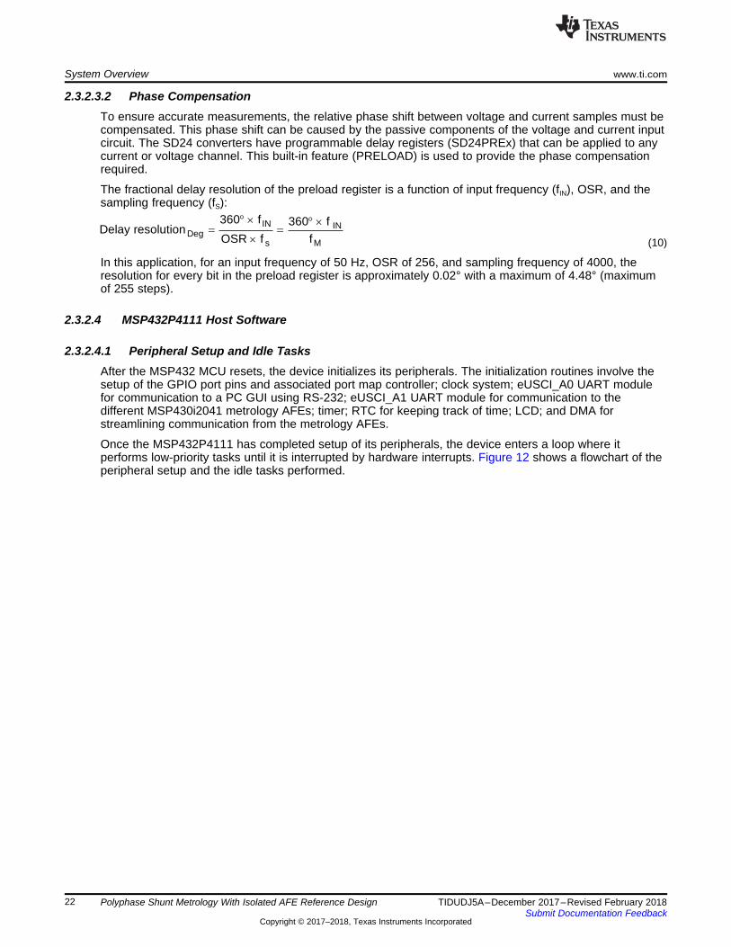
Once the MSP432P4111 has completed setup of its peripherals, the device enters a loop where itperforms low-priority tasks until it is interrupted by hardware interrupts. Figure 12 shows a flowchart of theperipheral setup and the idle tasks performed.
RESET
HW setup:Port pins, Clocks, RS-232 eUSCI, AFE
eUSCI, Timer, RTC, LCD, DMA
Parse data
New data to parse?
Y
Update LCD
DLT645 frame reception management
N
2 seconds elapsed?
RMS Voltage of a phase < Interruption_Threshold?
'LVDEOHSKDVHRUGHUUHDGLQJDQG³25´
phase_missing variable with (2* phase_identification)
(RMS Voltage of all phases > Interruption_Threshold) and (phase_missing nonzero)?
Alert timer ISR to send sync command, enable phase order reading again, and
set phase_missing=0
N N
Y Y
Y
www.ti.com System Overview
23TIDUDJ5A–December 2017–Revised February 2018Submit Documentation Feedback
Copyright © 2017–2018, Texas Instruments Incorporated
Polyphase Shunt Metrology With Isolated AFE Reference Design
Figure 12. Peripheral Setup and Idle Tasks
The first task performed in the loop is to process any received frames from the GUI. Next, the applicationchecks to see if there is new, noncritical data from any of the MSP430i2041 devices that need to beparsed (any critical data is parsed in the DMA interrupt service routine itself instead of in this loop). If thereis new data available to parse, the data is parsed and used to update the MSP432P4111's internalvariables if necessary. When there are new metrology parameters to parse and the RMS voltage isparsed, a check is made to determine if the RMS voltage reading of the phase is sufficiently larger than adefined interruption threshold. If the RMS voltage for the phase is below this threshold, then the phase is

System Overview www.ti.com
24 TIDUDJ5A–December 2017–Revised February 2018Submit Documentation Feedback
Copyright © 2017–2018, Texas Instruments Incorporated
Polyphase Shunt Metrology With Isolated AFE Reference Design
determined to be missing so the phase order calculations are disabled. If the RMS voltage for all phasesis above the interruption threshold after one or more phases were previously declared as missing, a synccommand is sent to all the MSP430i2041 devices and the phase order calculations are enabled again.Finally, the application checks to see if a new 2-second interval has elapsed since the last time the LCDhas been updated. The RTC keeps track of when a new 2-second interval has occurred and alerts thisLCD idle task of this new 2-second interval so that the LCD can be updated to display a new metrologyparameter.
2.3.2.4.2 Port 2 ISRWhenever any of the MSP430i2041 devices has just calculated new metrology parameters, theMSP430i2041 asserts a DRDY GPIO pin low to alert the MSP432 MCU that new parameters are nowready. The assertion of this MSP430i2041 GPIO pin specifically triggers the MSP432 Port 2 ISR. In thisISR, the application keeps track of the relative order of when the different DRDY pins are asserted. Wheneach phase's line voltage is available, this order of when the different DRDY pins are asserted determinethe phase sequence. In addition, the timer's count when a particular MSP430i2041's DRDY pin wasasserted is logged. This timer count is used by the timer ISR to determine the intentional delay that mustbe added before the MSP432 actually requests a phase's metrology parameters. In this reference design,the intentional delay from DRDY assertion to request of metrology parameters is 0 ms for phase A, 20 msfor phase B, and 40 ms for phase C. This delay ensures that there is enough time to get the metrologyparameters from a phase. In addition to using the timer count for adding intentional delays for metrologyparameters, this timer count also determines when a particular phase times out.
2.3.2.4.3 Timer ISRThe timer ISR is triggered at a rate of 4000 Hz. Every time this ISR is called, the timer_count_update andenergy_processing functions are called. The following two sections go over these functions.
2.3.2.4.3.1 timer_count_updateThe timer_count_update function serves two purposes. The first purpose is to send commands to theMSP430i2041 devices at the proper point in time. Whenever there is a request to send a sync commandto all the MSP430i2041 devices for ensuring correct phase sequence measurements, thetimer_count_update function is where this actual sync command is sent to the MSP430i2041 devices. Inaddition, this function is where the MSP432P4111 sends the commands to request metrology parametersfrom any MSP430i2041 device that has indicated through its DRDY GPIO pin that a new frame of datahas been calculated. To ensure that there is enough time to transfer the data packets from eachMSP430i2041 device, there is an intentional delay added from when the DRDY GPIO pin was asserted towhen the timer_count_update function requests the metrology parameters for a phase. The intentionaldelay from DRDY assertion to request of metrology parameters is 0 ms for phase A, 20 ms for phase B,and 40 ms for phase C. Whenever there is a request to get the calibration factors from a MSP430i2041device, the timer_count_update function is also where the actual request command for the calibrationfactor is sent to the MSP430i2041.
The second purpose of the timer_count_update function is to keep track of timeouts and to take theappropriate action when there is a timeout. The first set of timeouts managed by this function are triggeredwhen the previous set of metrology readings for a phase has been received more than approximately 1.05seconds ago. This timeout considers the scenario where the DRDY pin has been asserted by theMSP430i2041 and the MSP432 device has made a request for the new metrology parameters but it hasnot received a valid response from the MSP430i2041. In addition, this timeout also considers the scenariowhere the DRDY pin has not been asserted at all. This reference design has a separate timeout for eachindividual phase. Whenever a timeout occurs for a particular phase, the metrology parameters for thatassociated phase are set to 0 and a flag is asserted to let the application know that phase is missing. Thesecond set of timeouts managed by the timer_count_update function determine if a request has been sentto an MSP430i2041 device but a response has not been received within 0.25 seconds from when therequest was sent to specified MSP430i2041 device.

www.ti.com System Overview
25TIDUDJ5A–December 2017–Revised February 2018Submit Documentation Feedback
Copyright © 2017–2018, Texas Instruments Incorporated
Polyphase Shunt Metrology With Isolated AFE Reference Design
When a request for metrology readings or calibration factors has been sent to a specified MSP430i2041,any other requests for metrology readings or calibration factors are not made until the specifiedMSP430i2041 either gets the requested data or the specified command timeout for that phase occurs.Each time the MSP432P4111 requests a parameter from a specified MSP430i2041 device, thecorresponding MSP432 UART RX pin that is connected to that MSP430i2041 device is enabled bymodifying the port mapping controller to output the UART RX functionality on this pin. Simultaneously, theUART RX functionality is disabled from the UART RX pins for the other MSP430i2041 devices. If the two-channel mode is selected in this design, there is an additional step of also enabling the UART RX pin fromGPIO mode to peripheral mode. If the system is in two-channel mode and the MSP432P4111 gets arequested response from a specified MSP430i2041 device or there is a timeout for the request sent to theMSP430i2041, the shared DRDY/UART RX pin of the specified MSP430i2041 is set from UART RX pinmode to GPIO mode. Switching to GPIO mode enables the MSP432 MCU to detect the next time theMSP430i2041 has calculated new metrology parameters.
2.3.2.4.3.2 energy_processing
2.3.2.4.3.2.1 Pulse GenerationIn electricity meters, the active energy consumed is normally measured in fraction of kilowatt-hour (kWh)pulses. This information can be used to calibrate any meter for accurate measurement. The meter isresponsible for generating pulses proportional to the energy consumed.
This application uses average power to generate these energy pulses. If the absolute value of the averagepower is greater than the residual power cutoff value set in software, the average power is accumulatedduring every timer interrupt, thereby spreading the accumulated energy from the previous frame of dataevenly for each interrupt in the current 50 cycles frame. This is equivalent to converting it to energy. Whenthe accumulated energy crosses a threshold, a pulse is generated. The amount of energy above thisthreshold is kept and new energy value is added on top of it in the next interrupt cycle.
The residual power cutoff value is used to set the cutoff power reading at which the meter must notregister power readings. If the absolute value of a power reading is below this cutoff value, then the poweris not accumulated for the energy pulses. Additionally, if any phase's power reading is below this powercutoff value, then the corresponding cumulative energy reading used for pulse generation does notaccumulate that phase's power reading.
The threshold determines the energy "tick" specified by meter manufacturers and is a constant. A tick isusually defined in pulses per kWh or just in kWh. One pulse is generated for every energy tick. Forexample, in this application, the number of pulses generated per kWh is set to 6400 for active and reactiveenergies. The energy tick in this case is 1 kWh/6400. Energy pulses are generated and available on aheader and also through LEDs on the board. General-purpose I/O (port) pins are used to produce thepulses.

Timer interrupts at 4000 Hz
Energy Accumulator+= Average Power
Energy Accumulator > 1 tick(1/6400 kW)?
Energy Accumulator = Energy Accumulator ± 1 tick
Generate 1 pulse
Proceed to other tasks
Y
N
Absolute value ofaverage power >Residual Cutoff?
Y
N
System Overview www.ti.com
26 TIDUDJ5A–December 2017–Revised February 2018Submit Documentation Feedback
Copyright © 2017–2018, Texas Instruments Incorporated
Polyphase Shunt Metrology With Isolated AFE Reference Design
In the reference design, the LEDs that are labeled "Active" and "Reactive" correspond to the aggregateactive energy consumption and aggregate reactive energy consumption, respectively. The number ofpulses per kWh and each pulse duration can be configured in software. Figure 13 shows the flow diagramfor pulse generation. This flow diagram is valid for active and reactive energy.
Figure 13. Pulse Generation
The average power is in units of 0.001 W and the 1 kWh threshold is defined as:1-kWh threshold = (1 / 0.001) × 1 kW × (number of interrupts per second) × (number of seconds in onehour) = 1000000 × 4000 × 3600 = D18C2E28000

www.ti.com System Overview
27TIDUDJ5A–December 2017–Revised February 2018Submit Documentation Feedback
Copyright © 2017–2018, Texas Instruments Incorporated
Polyphase Shunt Metrology With Isolated AFE Reference Design
2.3.2.4.3.2.2 Energy BuffersIn addition to outputting energy pulses to indicate energy consumption, this reference design also storesthe total consumed energy readings into separate buffers, which can be seen from the PC GUI. Thesebuffers store the total amount of energy consumed since a system reset. The energy stored in theseenergy buffers are accumulated in a similar method as the energy used for pulse generation except adifferent energy tick is used. Instead of each tick corresponding to 1 kWh/6400 as is the case for pulsegeneration, the internal tick value corresponds to 0.1 Wh. This value means that the energy buffers in theMSP432P4111 software is in units of 0.1 Wh.
Similar to the energy used for pulse generation, the residual power cutoff value is used to set the cutoffpower reading at which the meter must not register power readings. If the absolute value of a powerreading is below this cutoff value, then the power is not accumulated into the energy buffers. Additionally,if any phase's power reading is below this power cutoff value, then the corresponding cumulative energybuffers does not accumulate that phase's power reading.
In this reference design, there are four sets of buffers that are available: one for each phase and one forthe cumulative of the phases. Within each set of buffers, the following energies are accumulated:1. Active import energy (active energy when active energy ≥ 0)2. Active export energy (active energy when active energy < 0)3. React. Quad I energy (reactive energy when reactive energy ≥ 0 and active power ≥ 0; inductive load)4. React. Quad II energy (reactive energy when reactive energy ≥ 0 and active power < 0; capacitive
generator)5. React. Quad III energy (reactive energy when reactive energy < 0 and active power < 0; inductive
generator)6. React. Quad IV energy (reactive energy when reactive energy < 0 and active power ≥ 0; capacitive
load)7. App. import energy (apparent energy when active energy ≥ 0)8. App. export energy (apparent energy when active energy < 0)
2.3.2.4.4 DMA1 ISRWhen the MSP432P4111 sends a request for metrology parameters or calibration factors to anMSP430i2041 device, the DMA module is used to place the packet response from the MSP430i2041 inmemory without CPU intervention. Once an entire packet is received, the DMA1 interrupt is triggered.Figure 14 shows the flowchart of the DMA1 ISR. In this ISR, the application calculates a checksum andcompares it to the checksum value in the packet sent. The checksum is calculated by adding eachelement in the packet except the final byte, which is the checksum, and then taking a logical OR of thecalculated checksum with 0xFF. If the checksum passes, any critical portions of the packet are parsed inthe ISR, an alert is made to the idle task to parse other portions of the packet, the DRDY/UART RX pin isconfigured back to a GPIO pin when in two-channel mode, and transmission of other commands to theMSP430i2041 devices is enabled again.
When a request for metrology parameters is sent to an MSP430i2041 device and the received packetdoes not pass the checksum check, the MSP432 MCU sends a duplicate request for the packet. If thepacket received does not pass the checksum check for a second consecutive time, no further requests aresent for metrology parameters until the MSP430i2041 alerts the MSP432P4111 of new metrologyparameters being ready through its DRDY GPIO pin.

Calculate sumcheck over all bytes of the received packet
except the last byte
Parse critical data, provide alert to parse noncritical data
in idle task loop, change DRDY/UART RX pin to input
GPIO mode, enable transmission of commands to
MSP430i2041 devices,
(Sumcheck & 0xFF) =last byte of packet?
Y
Resend request for metrology readings and set Retry=1
NPacket received was a response for metrology parameter request?
DMA1 Interrupt
Retry=0?
Set Retry=0, change DRDY/UART RX pin to input GPIO mode, enable transmission of commands to
MSP430i2041 devices
N
Return
Y
Y
N
System Overview www.ti.com
28 TIDUDJ5A–December 2017–Revised February 2018Submit Documentation Feedback
Copyright © 2017–2018, Texas Instruments Incorporated
Polyphase Shunt Metrology With Isolated AFE Reference Design
Figure 14. DMA1 ISR
2.3.2.5 MSP430i2041-to-MSP432P4111 CommunicationThe MSP432P4111 can send five primary commands to the MSP430i2041 devices. These commandsobtain metrology readings for a phase, perform metrology calibration, and synchronize the differentMSP430i2041 devices for phase sequence detection. When the MSP430i2041 receives a command fromthe MSP432 device and is in two-channel mode, the MSP430i2041 configures its shared DRDY/UART TXpin from GPIO mode to UART mode. Based on the received command from the MSP432 MCU, theMSP430i2041 device performs any required actions and, if necessary, sends a response packet back tothe MSP432P4111.
For specifically receiving a phase's metrology parameters from a particular MSP430i2041 device, theHOST_CMD_GET_READINGS_n command is sent by the MSP432 MCU, where the n value correspondsto the phase and has a value of either 1 (for phase A), 2 (for phase B) or 3 (for phase C). The n value isused by the MSP432 device to request the parameters for a specific phase by having the differentHOST_CMD_GET_READINGS_n commands have different command byte values. For example, if theMSP432 device wants the metrology parameters for Phase A, the MSP432 device sends theHOST_CMD_GET_READINGS_1 command to all the MSP430i2041 devices. The device that has aphase ID (as configured by the voltages present on the two phase-identification GPIO pins) thatcorresponds to Phase A then responds with its metrology parameters while the other phases ignore therequest.
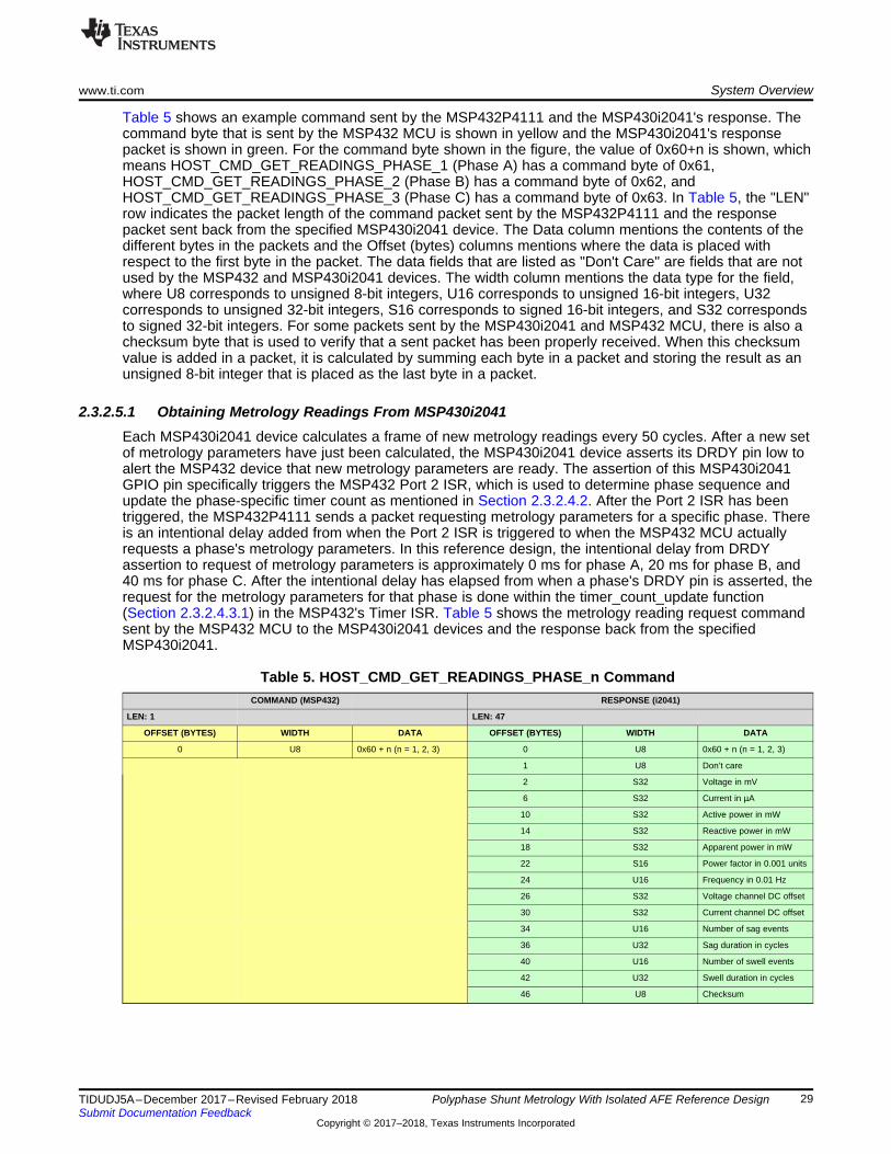
www.ti.com System Overview
29TIDUDJ5A–December 2017–Revised February 2018Submit Documentation Feedback
Copyright © 2017–2018, Texas Instruments Incorporated
Polyphase Shunt Metrology With Isolated AFE Reference Design
Table 5 shows an example command sent by the MSP432P4111 and the MSP430i2041's response. Thecommand byte that is sent by the MSP432 MCU is shown in yellow and the MSP430i2041's responsepacket is shown in green. For the command byte shown in the figure, the value of 0x60+n is shown, whichmeans HOST_CMD_GET_READINGS_PHASE_1 (Phase A) has a command byte of 0x61,HOST_CMD_GET_READINGS_PHASE_2 (Phase B) has a command byte of 0x62, andHOST_CMD_GET_READINGS_PHASE_3 (Phase C) has a command byte of 0x63. In Table 5, the "LEN"row indicates the packet length of the command packet sent by the MSP432P4111 and the responsepacket sent back from the specified MSP430i2041 device. The Data column mentions the contents of thedifferent bytes in the packets and the Offset (bytes) columns mentions where the data is placed withrespect to the first byte in the packet. The data fields that are listed as "Don't Care" are fields that are notused by the MSP432 and MSP430i2041 devices. The width column mentions the data type for the field,where U8 corresponds to unsigned 8-bit integers, U16 corresponds to unsigned 16-bit integers, U32corresponds to unsigned 32-bit integers, S16 corresponds to signed 16-bit integers, and S32 correspondsto signed 32-bit integers. For some packets sent by the MSP430i2041 and MSP432 MCU, there is also achecksum byte that is used to verify that a sent packet has been properly received. When this checksumvalue is added in a packet, it is calculated by summing each byte in a packet and storing the result as anunsigned 8-bit integer that is placed as the last byte in a packet.
2.3.2.5.1 Obtaining Metrology Readings From MSP430i2041Each MSP430i2041 device calculates a frame of new metrology readings every 50 cycles. After a new setof metrology parameters have just been calculated, the MSP430i2041 device asserts its DRDY pin low toalert the MSP432 device that new metrology parameters are ready. The assertion of this MSP430i2041GPIO pin specifically triggers the MSP432 Port 2 ISR, which is used to determine phase sequence andupdate the phase-specific timer count as mentioned in Section 2.3.2.4.2. After the Port 2 ISR has beentriggered, the MSP432P4111 sends a packet requesting metrology parameters for a specific phase. Thereis an intentional delay added from when the Port 2 ISR is triggered to when the MSP432 MCU actuallyrequests a phase's metrology parameters. In this reference design, the intentional delay from DRDYassertion to request of metrology parameters is approximately 0 ms for phase A, 20 ms for phase B, and40 ms for phase C. After the intentional delay has elapsed from when a phase's DRDY pin is asserted, therequest for the metrology parameters for that phase is done within the timer_count_update function(Section 2.3.2.4.3.1) in the MSP432's Timer ISR. Table 5 shows the metrology reading request commandsent by the MSP432 MCU to the MSP430i2041 devices and the response back from the specifiedMSP430i2041.
Table 5. HOST_CMD_GET_READINGS_PHASE_n CommandCOMMAND (MSP432) RESPONSE (i2041)
LEN: 1 LEN: 47
OFFSET (BYTES) WIDTH DATA OFFSET (BYTES) WIDTH DATA
0 U8 0x60 + n (n = 1, 2, 3) 0 U8 0x60 + n (n = 1, 2, 3)
1 U8 Don’t care
2 S32 Voltage in mV
6 S32 Current in µA
10 S32 Active power in mW
14 S32 Reactive power in mW
18 S32 Apparent power in mW
22 S16 Power factor in 0.001 units
24 U16 Frequency in 0.01 Hz
26 S32 Voltage channel DC offset
30 S32 Current channel DC offset
34 U16 Number of sag events
36 U32 Sag duration in cycles
40 U16 Number of swell events
42 U32 Swell duration in cycles
46 U8 Checksum

Select new phase
GUI sends message to MSP432 UHTXHVWLQJSKDVH¶VFDOLEUDWLRQ
factors
Timer_count_update function in timer ISR sends command to all the MSP430i2041 devices for the SKDVH¶VFDOLEUDWLRQIDFWRUVDQG
setups DMA to read 31 byte packet response from MSP430i2041
MSP432 currentlysending or
waiting for data from a MSP430i2041 device?
N
Y
MSP430i2041 device of requested phase sends
calibration factors in 31 byte packet
DMA1 ISR
Calibration factors parsed in idle task loop and used to update MSP432's copy of calibration
factors. Set flag to indicate new calibration factors received.
Continue waiting until current packet is sent or received and
performing other tasks
Calibration factors of all phases received?
N
All calibration factors have now been received
Timeout for the GUI not receiving a response message
back causes the PC GUI to send a repeat message to
MSP432 UHTXHVWLQJSKDVH¶Vcalibration factors
MSP432 device sends new calibration factors recently
parsed to the PC GUI
Y
PC GUI MSP432 MSP430i2041
System Overview www.ti.com
30 TIDUDJ5A–December 2017–Revised February 2018Submit Documentation Feedback
Copyright © 2017–2018, Texas Instruments Incorporated
Polyphase Shunt Metrology With Isolated AFE Reference Design
The MSP430i2041's response provides results based on real world units. As an example, the active powerreading sent in the response packet is in units of mW so an active power value of 2300134 in this packetwould correspond to 2300.123 W.
In this application, after the MSP432P4111 sends the HOST_CMD_GET_READINGS_PHASE_ncommand, the MCU configures its DMA to read the 47 byte response from the MSP430i2041 withoutrequiring CPU intervention. After the 47-byte response has been received by the MSP432P4111, theDMA1 ISR is triggered and the critical portions of the packet are parsed as described in Section 2.3.2.4.4.The noncritical portions of the packet are parsed in the idle task loop mentioned in Section 2.3.2.4.1.
2.3.2.5.2 Metrology CalibrationMetrology calibration is performed by changing calibration factors that are stored on the MSP430i2041devices. In this reference design, the PC GUI calibrates the metrology. When performing calibration, thePC GUI first sends commands to the MSP432P4111 to request the calibration factors of the differentphases until the calibration factors of all the phases have been received. Figure 15 summarizes theprocess used for the GUI to obtain the calibration factors for all the phases.
Figure 15. Process for Obtaining All Calibration Factors
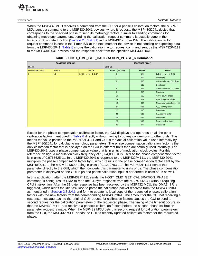
www.ti.com System Overview
31TIDUDJ5A–December 2017–Revised February 2018Submit Documentation Feedback
Copyright © 2017–2018, Texas Instruments Incorporated
Polyphase Shunt Metrology With Isolated AFE Reference Design
When the MSP432 MCU receives a command from the GUI for a phase's calibration factors, the MSP432MCU sends a command to the MSP430i2041 devices, where it requests the MSP430i2041 device thatcorresponds to the specified phase to send its metrology factors. Similar to sending commands forobtaining metrology parameters, sending the calibration request command is actually done in thetimer_count_update function (Section 2.3.2.4.3.1) in the MSP432's Timer ISR. The calibration factorrequest command is sent in the Timer ISR at the next moment the device is not sending or expecting datafrom the MSP430i2041. Table 6 shows the calibration factor request command sent by the MSP432P4111to the MSP430i2041 devices and the response back from the specified MSP430i2041.
Table 6. HOST_CMD_GET_CALIBRATION_PHASE_n CommandCOMMAND (MSP432) RESPONSE (i2041)
LEN: 1 LEN: 31
OFFSET (BYTES) WIDTH DATA OFFSET (BYTES) WIDTH DATA
0 U8 0xD5 + n (n = 1, 2, 3) 0 U8 0xD5 + n (n = 1, 2, 3)
1 U8 Don’t care
2 S16 Voltage channel DC offset
4 S16 Don’t care
6 S16 Current channel DC offset
8 S16 Don’t care
10 S32 Active power offset
14 S32 Reactive power offset
18 S16 Phase correction factor × 8
20 U16 VRMS scaling factor
22 S16 Don’t care
24 U16 IRMS scaling factor
26 U16 Don’t care
28 U16 Power scaling factor
30 U8 Checksum
Except for the phase compensation calibration factor, the GUI displays and operates on all the othercalibration factors mentioned in Table 6 directly without having to do any conversions to other units. Thismeans the value passed to the MSP432P4111 and GUI is the actual calibration value used internally bythe MSP430i2041 for calculating metrology parameters. The phase compensation calibration factor is theonly calibration factor that is displayed on the GUI in different units than are actually used internally. TheMSP430i2041 uses a phase compensation value that is in units of modulation clock cycles. For thisreference design, a modulation clock frequency of 1,024,000 Hz is used so the phase compensation factoris in units of 0.9765625 µs. In the MSP430i2041's response to the MSP432P4111, the MSP430i2041multiplies the phase compensation factor by 8, which results in the phase compensation factor sent by theMSP40i2041 to the MSP432 MCU being in units of 0.1220703 µs. The MSP432P4111 sends thisparameter directly to the GUI, which then converts this parameter to units of µs. The phase compensationparameter is displayed on the GUI in µs and phase calibration input is performed in units of µs as well.
In this application, after the MSP432P4111 sends the HOST_CMD_GET_CALIBRATION_PHASE_ncommand, it configures its DMA to read the 31-byte response from the MSP430i2041 without requiringCPU intervention. After the 31-byte response has been received by the MSP432 MCU, the DMA1 ISR istriggered, which alerts the idle task loop to parse the calibration packet received from the MSP430i2041as mentioned in Section 2.3.2.4.1 and for it to update its local copy of the requested phase's calibrationfactors with the new factors from the corresponding MSP430i2041. The timeout for the GUI not receiving aresponse message back to the original GUI request for calibration factors causes the GUI to send asecond request for the calibration parameters of the requested phase. The timing of the timeout occurs sothat the MSP432P4111 has received a phase's calibration factors before the second-phase calibrationparameter request is made. When the MSP432 MCU gets this second request for calibration parametersfrom the GUI, the MSP432P4111 sends the GUI its recently updated calibration factors for the requestedphase.

Select new phase
GUI sends new calibration factor for the phase to the MSP432
MSP430i2041 device of requested phase updates calibration factors to new
calibration parameters received, disables performing metrology calculations, and
sends response packet to MSP432
Disable interrupts and send updated phase calibration factors to MSP430i2041
New calibration factors sent for all phases?
N
All calibration factors have now been updated
Y
PC GUI MSP432 MSP430i2041
6HQG³DOLJQWRFDOLEUDWLRQIDFWRUV´
command to all MSP430i2041 devicesRestart sigma delta converter and enable
performing metrology calculations
Enable interrupts and send message to PC GUI to let it know that the phase has
been successfully calibrated
System Overview www.ti.com
32 TIDUDJ5A–December 2017–Revised February 2018Submit Documentation Feedback
Copyright © 2017–2018, Texas Instruments Incorporated
Polyphase Shunt Metrology With Isolated AFE Reference Design
After all the calibration factors have been received from all the MSP430i2041 devices, the GUI uses theerror inputted into the GUI to calculate new calibration parameters for all the phases. The calibrationfactors for each phase are then sent one by one to the MSP432P4111 until the calibration factors of all thephases have been sent. The process of setting the new calibration factors is summarized in Figure 16.
Figure 16. Process for Setting New Calibration Factors
When the MSP432P4111 receives a phase's new calibration factors, it disables interrupts then sends outthe HOST_CMD_SET_CALIBRATION_PHASE_n packet to the MSP430i2041 devices so that thespecified MSP430i2041 device could update its calibration factors accordingly. Then waits for an expectedresponse from the MSP430i2041 device to let it know that the MSP430i2041 device has finished updatingits calibration factors. Once the MSP430i2041 device receives the new calibration factors, it disablesperforming metrology calculations, updates its metrology calibration factors, and sends a response back tothe MSP432 device.

www.ti.com System Overview
33TIDUDJ5A–December 2017–Revised February 2018Submit Documentation Feedback
Copyright © 2017–2018, Texas Instruments Incorporated
Polyphase Shunt Metrology With Isolated AFE Reference Design
Table 7 shows the HOST_CMD_SET_CALIBRATION_PHASE_n packet sent to the MSP430i2041 and itsresponse packet. In the packet sent to the MSP430i2041 device, the phase compensation factor is in units8 times smaller than the internal phase compensation value used by the MSP430i2041 device so thephase compensation value in the packet is divided by 8 before being set as the MSP430i2041's newphase compensation value.
Table 7. HOST_CMD_SET_CALIBRATION_PHASE_n CommandCOMMAND (MSP432) RESPONSE (i2041)
LEN: 31 LEN: 2
OFFSET (BYTES) WIDTH DATA OFFSET (BYTES) WIDTH DATA
0 U8 0xD0 + n (n = 1, 2, 3) 0 U8 0xD0 + n (n = 1, 2, 3)
1 U8 Don’t care 1 U8 0xD0 + n (n = 1, 2, 3)
2 S16 Voltage channel DC offset
4 S16 Don’t care
6 S16 Current channel DC offset
8 S16 Don’t care
10 S32 Active power offset
14 S32 Reactive power offset
18 S16 Phase correction factor × 8
20 U16 VRMS scaling factor
22 S16 Don’t care
24 U16 IRMS scaling factor
26 U16 Don’t care
28 U16 Power scaling factor
30 U8 Checksum
When the MSP432 device has received a valid response from the MSP430i2041 device that it sentcalibration factors to, the MSP432 MCU sends a HOST_CMD_ALIGN_WITH_CALIBRATION_FACTORScommand to all the MSP430i2041 devices. Table 8 shows theHOST_CMD_ALIGN_WITH_CALIBRATION_FACTORS packet sent to the MSP430i2041 devices. Thiscommand is used to enable performing metrology calculations after any MSP430i2041 device hasreceived a HOST_CMD_SET_CALIBRATION_PHASE_n command addressed to it. TheHOST_CMD_ALIGN_WITH_CALIBRATION_FACTORS differs from the other calibration factors in that itis intended to be sent to all the MSP430i2041 devices so there are not different variations of thiscommand for different phases. When each device receives this command, they all perform the sameactions. In addition, the MSP430i2041 devices do not send a response packet when they receive thiscommand. After the MSP432 device has sent the HOST_CMD_ALIGN_WITH_CALIBRATION_FACTORScommand, the MSP432P4111 enables interrupts again and sends a message to the GUI to let it know thatcalibration has been successfully completed on the phase it sent calibration factors for and the GUI cansend the updated parameter for the next phase until all of the phase calibration factors have been sent.
Table 8. HOST_CMD_ALIGN_WITH_CALIBRATION_FACTORS CommandCOMMAND (MSP432) RESPONSE (i2041)
LEN: 1 LEN: 0
OFFSET (BYTES) WIDTH DATA OFFSET (BYTES) WIDTH DATA
0 U8 0x5A
System Overview www.ti.com
34 TIDUDJ5A–December 2017–Revised February 2018Submit Documentation Feedback
Copyright © 2017–2018, Texas Instruments Incorporated
Polyphase Shunt Metrology With Isolated AFE Reference Design
2.3.2.5.3 Synchronizing MSP430i2041 Devices for Phase Sequence DetectionEvery 50 mains cycles, each MSP430i2041 outputs a pulse on the DRDY pin to indicate that newmetrology parameters are ready. The delay from the last leading zero crossing to the assertion of theDRDY pin is fixed and does not vary significantly across MSP43i2041 devices, which allows the user todetermine the phase sequence by noting the order at which the DRDY pin is asserted when the devicesare synchronized to start from the same starting point. To synchronize the different MSP430i2041 devicesto start from the same starting point, the HOST_CMD_SEND_SYNC command is sent to all theMSP430i2041 devices at the same time. Table 9 shows the HOST_CMD_SEND_SYNC packet sent to theMSP430i2041 devices. Similar to the HOST_CMD_ALIGN_WITH_CALIBRATION_FACTORS command,the MSP430i2041 devices do not send a response back after they receive the HOST_CMD_SEND_SYNCcommand.
Table 9. HOST_CMD_SEND_SYNC CommandCOMMAND (MSP432) RESPONSE (i2041)
LEN: 1 LEN: 0
OFFSET (BYTES) WIDTH DATA OFFSET (BYTES) WIDTH DATA
0 U8 0xDB
As mentioned in Section 2.3.2.3.1, when a MSP430i2041 device receives a sync command, the deviceclears the current count of the cycle_count variable used to trigger the foreground process so that all thedifferent MSP430i2041 devices would start counting cycles from the same mains cycle at the next time theDRDY pins are asserted.
The HOST_CMD_SEND_SYNC is sent by the MSP432P4111 each time one of the phases has gonemissing and then returns so that all of the phases are available again. A phase is determined as beingmissing whenever the parsed RMS voltage is below an interruption threshold (as mentioned inSection 2.3.2.4.1) or whenever a DRDY pulse has not been received from the phase in the last 1.05seconds. Similar to sending commands for obtaining calibration parameters, sending theHOST_CMD_SEND_SYNC command is actually done in the timer_count_updatefunction(Section 2.3.2.4.3.1 ) in the MSP432's Timer ISR. The calibration factor request command is sentin the Timer ISR at the next moment the device is not sending or expecting data from the MSP430i2041device.

www.ti.com Hardware, Software, Testing Requirements, and Test Results
35TIDUDJ5A–December 2017–Revised February 2018Submit Documentation Feedback
Copyright © 2017–2018, Texas Instruments Incorporated
Polyphase Shunt Metrology With Isolated AFE Reference Design
3 Hardware, Software, Testing Requirements, and Test Results
3.1 Required Hardware and Software
3.1.1 Cautions and WarningsAt high currents, the terminal block can get warm. In addition, note that the MSP430i2041 devices arereferenced with respect to the different phase voltages, so take the proper precautions.
WARNING
Hot Surface! Contact can cause burns. Do not touch.Take the proper precautions when operating.
CAUTION
High Voltage! Electric shocks are possible when connecting theboard to live wires. The board must be handled with care by a professional. Forsafety, use of isolated test equipment with overvoltage or overcurrent protectionis highly recommended.

Phase C
Metrology F
ront-End
Phase B
Metrology F
ront-End
Phase A
Metrology F
ront-End
MSP432
MSP432JTAG
LCD
Isol
ated
RS
-232
LED
S
Pulses MSP432 Power
Hardware, Software, Testing Requirements, and Test Results www.ti.com
36 TIDUDJ5A–December 2017–Revised February 2018Submit Documentation Feedback
Copyright © 2017–2018, Texas Instruments Incorporated
Polyphase Shunt Metrology With Isolated AFE Reference Design
3.1.2 HardwareThe following figures of the EVM best describe the hardware: Figure 17 is the top view of the energymeasurement system, and Figure 18 shows the location of various pieces of the design based onfunctionality.
Figure 17. Top View of Reference Design Figure 18. Top View of Reference Design WithComponents Highlighted
3.1.2.1 Connections to the Test Setup for AC VoltagesAC voltages can be applied to the board for testing purposes at these points:• Pad "LINE1" corresponds to the line connection for phase A.• Pad "LINE2" corresponds to the line connection for phase B.• Pad "LINE3" corresponds to the line connection for phase C.• Pad "N" corresponds to the neutral voltage. The voltage between any of the three line connections to
the neutral connection must not exceed 230-V AC at 50 and 60 Hz.• I1+, I1−, and I1Live are connected to the output terminals of the shunt that is used for measuring the
current for Phase A. When a shunt is selected, the differential voltage that is output across I1+ and I1−must not exceed 58 mV.
• I2+, I2−, and I2Live are connected to the output terminals of the shunt that is used for measuring thecurrent for Phase B. When a shunt is selected, the differential voltage that is output across I2+ and I2−must not exceed 58 mV.
• I3+, I3−, and I3Live are connected to the output terminals of the shunt that is used for measuring thecurrent for Phase C. When a shunt is selected, the differential voltage that is output across I3+ and I3−must not exceed 58 mV.

I A+(I
1+)
I A-(I
1-)
VA
+(I
1Liv
e)
www.ti.com Hardware, Software, Testing Requirements, and Test Results
37TIDUDJ5A–December 2017–Revised February 2018Submit Documentation Feedback
Copyright © 2017–2018, Texas Instruments Incorporated
Polyphase Shunt Metrology With Isolated AFE Reference Design
Figure 19 shows a mapping between shunt terminals and I1 (Phase A) current pads. A similar mapping isdone between the other shunts and corresponding phases.
Figure 19. Mapping Between Shunt Terminals and Ix Current Pads
Figure 20 and Figure 21 show the various connections that must be made to the test setup for properfunctionality of the EVM. When a test AC source must be connected, the connections have to be madeaccording to the EVM design. When a test AC source must be connected, the links on the board must beconnected as shown in Figure 20.

VC+
IC+ IC-
VB+
IB+ IB-
VA+
IA+ IA-
VN
Link Closed
Hardware, Software, Testing Requirements, and Test Results www.ti.com
38 TIDUDJ5A–December 2017–Revised February 2018Submit Documentation Feedback
Copyright © 2017–2018, Texas Instruments Incorporated
Polyphase Shunt Metrology With Isolated AFE Reference Design
Figure 20. Top View of EVM With Links Closed
Figure 21 shows the connections from the front view. VA+, VB+, and VC+ correspond to the line voltagesfor phases A, B, and C, respectively. VN corresponds to the neutral voltage from the test AC source. IA+and IA− correspond to the current inputs for phase A, IB+, and IB− correspond to the current inputs forphase B; IC+ and IC− correspond to the current inputs for phase C. VN corresponds to the neutral voltagefrom the test setup.
Figure 21. Front View of EVM With Test Setup Connections
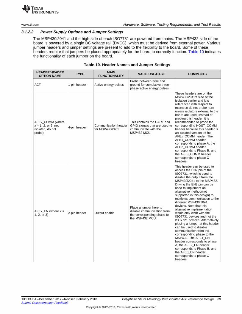
www.ti.com Hardware, Software, Testing Requirements, and Test Results
39TIDUDJ5A–December 2017–Revised February 2018Submit Documentation Feedback
Copyright © 2017–2018, Texas Instruments Incorporated
Polyphase Shunt Metrology With Isolated AFE Reference Design
3.1.2.2 Power Supply Options and Jumper SettingsThe MSP430i2041 and the high-side of each ISO7731 are powered from mains. The MSP432 side of theboard is powered by a single DC voltage rail (DVCC), which must be derived from external power. Variousjumper headers and jumper settings are present to add to the flexibility to the board. Some of theseheaders require that jumpers be placed appropriately for the board to correctly function. Table 10 indicatesthe functionality of each jumper on the board.
Table 10. Header Names and Jumper Settings
HEADER/HEADEROPTION NAME TYPE MAIN
FUNCTIONALITY VALID USE-CASE COMMENTS
ACT 1-pin header Active energy pulsesProbe between here andground for cumulative three-phase active energy pulses.
AFEx_COMM (wherex = 1, 2, or 3; notisolated, do notprobe)
4-pin header Communication headerfor MSP430i2401
This contains the UART andGPIO signals that are used tocommunicate with theMSP432 MCU.
These headers are on theMSP430i2041's side of theisolation barrier and it isreferenced with respect tomains so do not probe hereunless isolators external to theboard are used. Instead ofprobing this header, it isrecommended to probe thecorresponding HOST_COMMheader because this header isan isolated version oft heAFEx_COMM header. TheAFE1_COMM headercorresponds to phase A, theAFE2_COMM headercorresponds to Phase B, andthe AFE3_COMM headercorresponds to phase Cheaders.
AFEx_EN (where x =1, 2, or 3) 2-pin header Output enable
Place a jumper here todisable communication fromthe corresponding phase tothe MSP432 MCU.
This header can be used toaccess the EN2 pin of theISO7731, which is used todisable the output from theMSP430i2041 to the MSP432.Driving the EN2 pin can beused to implement analternative method(notsupported in this design) tomultiplex communication to thedifferent MSP430i2041devices. Note that thisalternative implementationwould only work with theISO7731 devices and not theISO7721 devices. Alternatively,placing a jumper at this headercan be used to disablecommunication from thecorresponding phase to theMSP432. The AFE1_ENheader corresponds to phaseA, the AFE2_EN headercorresponds to Phase B, andthe AFE3_EN headercorresponds to phase Cheaders.
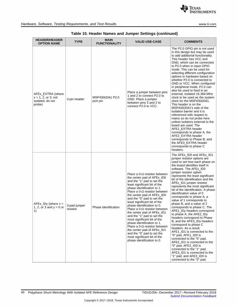
Hardware, Software, Testing Requirements, and Test Results www.ti.com
40 TIDUDJ5A–December 2017–Revised February 2018Submit Documentation Feedback
Copyright © 2017–2018, Texas Instruments Incorporated
Polyphase Shunt Metrology With Isolated AFE Reference Design
Table 10. Header Names and Jumper Settings (continued)HEADER/HEADER
OPTION NAME TYPE MAINFUNCTIONALITY VALID USE-CASE COMMENTS
AFEx_EXTRA (wherex = 1, 2, or 3; notisolated, do notprobe)
3-pin header MSP430i2041 P2.0port pin
Place a jumper between pins1 and 2 to connect P2.0 toGND. Place a jumperbetween pins 3 and 2 toconnect P2.0 to VCC.
The P2.0 GPIO pin is not usedin this design but may be usedto add additional functionality.This header has VCC andGND, which can be connectedto P2.0 when in input GPIOmode. This can be used forselecting different configurationoptions in hardware based onwhether P2.0 is connected toGND or VCC. When configuredin peripheral mode, P2.0 canalso be used to feed in anexternal, isolated 16.384-MHzclock to be used as the systemclock for the MSP430i2041.This header is on theMSP430i2041's side of theisolation barrier and it isreferenced with respect tomains so do not probe hereunless isolators external to theboard are used. TheAFE1_EXTRA headercorresponds to phase A, theAFE2_EXTRA headercorresponds to Phase B, andthe AFE3_EXTRA headercorresponds to phase Cheaders.
AFEx_IDy (where x =1, 2, or 3 and y = 0 or1)
3-pad jumperresistor Phase identification
Place a 0-Ω resistor betweenthe center pad of AFEx_ID0and the "1" pad to set theleast significant bit of thephase identification to 1.Place a 0-Ω resistor betweenthe center pad of AFEx_ID0and the "0" pad to set theleast significant bit of thephase identification to 0.Place a 0-Ω resistor betweenthe center pad of AFEx_ID1and the "1" pad to set themost significant bit of thephase identification to 1.Place a 0-Ω resistor betweenthe center pad of AFEx_ID1and the "0" pad to set themost significant bit of thephase identification to 0.
The AFEx_ID0 and AFEx_ID1jumper resistor options areused to set how each phase onthe board identifies itself insoftware. The AFEx_ID0jumper resistor optionrepresents the least significantbit of the identification and theAFEx_ID1 jumper resistorrepresents the most significantbit of the identification. A phaseidentification value of 0corresponds to phase A, avalue of 1 corresponds tophase B, and a value of 2corresponds to phase C. TheAFE1_IDy headers correspondto phase A, the AFE2_IDyheaders correspond to PhaseB, and the AFE3_IDy headerscorrespond to phase Cheaders. As a result,AFE1_ID1 is connected to the"0" pad, AFE1_ID0 isconnected to the "0" pad,AFE2_ID1 is connected to the"0" pad, AFE2_ID0 isconnected to the "1" pad,AFE3_ID1 is connected to the"1" pad, and AFE3_ID0 isconnected to the "0" pad.

www.ti.com Hardware, Software, Testing Requirements, and Test Results
41TIDUDJ5A–December 2017–Revised February 2018Submit Documentation Feedback
Copyright © 2017–2018, Texas Instruments Incorporated
Polyphase Shunt Metrology With Isolated AFE Reference Design
Table 10. Header Names and Jumper Settings (continued)HEADER/HEADER
OPTION NAME TYPE MAINFUNCTIONALITY VALID USE-CASE COMMENTS
AFEx_JTAG (where x= 1, 2, or 3; notisolated, do notprogram whenconnected to Mains)
4-pin header2-wire JTAGprogramming option(WARNING)
To program the MSP430i2041devices, configure AFEPWRxheader to the external poweroption. In addition, connectpin 1 of this header to pin 2 ofthe MSP-FET tool, pin 2 ofthis header to pin 1 of theMSP-FET tool, pin 3 of thisheader to pin 7 of the MSP-FET tool , and pin 4 of thisheader to pin 9 of the MSP-FET tool.
Do not program theMSP430i2041 devices with theboard connected to AC mains.The AFE1_JTAG headercorresponds to phase A, theAFE2_JTAG headercorresponds to Phase B, andthe AFE3_JTAG headercorresponds to phase Cheaders.
AFEx_OPTy (where x= 1, 2, or 3 and y = 1,2, or 3)
3-pad jumperresistor
Additional GPIO portpins
Place a 0-Ω resistor betweenthe center pad and "GND"pad, to connect the GPIO pinto GND. Place a 0-Ω resistorbetween the center pad andthe "VCC" pad to connect theGPIO pin to VCC.
These GPIO pins are not usedin this design but can be usedto add additional functionality.These GPIO pins can beconnected to VCC or GND byplacing a 0 Ohm resistor at theappropriate pads. This can beused for selecting differentconfiguration options inhardware based on whetherthe GPIO pins are connectedto GND or VCC. TheAFE1_OPTy headerscorresponds to phase A, theAFE2_OPTy headerscorresponds to Phase B, andthe AFE3_OPTy headerscorresponds to phase Cheaders. AFEx_OPT1 optionsare connected to the P2.3GPIO pins, AFEx_OPT2options are connected to theP1.7 GPIO pins, andAFEx_OPT3 options areconnected to the P1.0 GPIOpins
AFEPWRx (where x =1,2, or 3) 3-pin header
Selection for the high-side power supply for aphase
This header is used to selectthe power source for theMSP430i2041 and ISO7731of a phase.
To enable powering the high-side using the onboard cap-drop supply, place a jumperbetween pins 1 and 2 of thisheader. To enable poweringthe high side by externalpower, place a jumper betweenpins 2 and 3 of this header.The external power can beapplied at any other GND andVCC header option locationsfor the phase. An examplelocation to connect externalpower to includes terminalblock U$13 for phase A,terminal block U$17 for phaseB, and terminal block U$14 forphase C. When programmingthe MSP430i2041 devices,make sure that the jumper isconnected to the externaloption and mains is notenabled. The AFEPWR1header corresponds to phaseA, the AFEPWR2 headercorresponds to Phase B, andthe AFEPWR3 headercorresponds to phase Cheaders.

Hardware, Software, Testing Requirements, and Test Results www.ti.com
42 TIDUDJ5A–December 2017–Revised February 2018Submit Documentation Feedback
Copyright © 2017–2018, Texas Instruments Incorporated
Polyphase Shunt Metrology With Isolated AFE Reference Design
Table 10. Header Names and Jumper Settings (continued)HEADER/HEADER
OPTION NAME TYPE MAINFUNCTIONALITY VALID USE-CASE COMMENTS
DGND Header Ground voltage header
Not a jumper header, probehere for GND voltage.Connect negative terminal ofbench or external powersupply when powering theboard externally.
DVCC Header VCC voltage header
Not a jumper header, probehere for VCC voltage.Connect positive terminal ofbench or external powersupply when powering theboard externally.
HOST_COMMx(where x = 1, 2, or 3) 4-pin header Communication header
for MSP432
This contains the UART andGPIO signals that are used tocommunicate with theMSP430i2041 devices.
These headers are on theMSP432's side of the isolationbarrier, which is isolated frommains so they are safe toprobe. The HOST_COMM1header corresponds to theisolated version of theAFE1_COMM header. TheHOST_COMM2 headercorresponds to the isolatedversion of the AFE2_COMMheader. The HOST_COMM3header corresponds to theisolated version of theAFE3_COMM header.
HOST_EXTRA 3-pin header External clockgeneration output
This design has a footprintthat allows placing a clockgenerator (footprint is labeledCLK_GEN on the PCB) thatcan be used to generate aclock signal. When using thisoption, populating the clockgenerator footprint (notpopulated by default) andplacing a 0-Ω resistor at R1(also not populated bydefault) connects thegenerated clock to thisheader.
INB_SELx (where x =1, 2, or 3 and y = 1,2, or 3)
3-pad jumperresistor
ISO7731 INB channelselection
Place a 0-Ω resistor betweenthe center pad and "UTSI"pad to configure this design touse UART. Place a 0-Ωresistor between the centerpad and "URSO" pad toconfigure this design to useSPI. Because this design'ssoftware uses UART forcommunication instead ofSPI, make sure to place a 0-Ω resistor at the "UTSI" pad,which would connect theMSP430i2041's UART TXsignal to the MSP432'scorresponding UART RXsignal for that phase.
Do not connect an input pin tothe INB pin. This jumperresistor ensures thisconnection does not occurregardless if the hardwaresupports SPI or UARTcommunication. The INB_SEL1header corresponds to phaseA, the INB_SEL2 headercorresponds to Phase B, andthe INB_SEL3 headercorresponds to phase Cheaders.
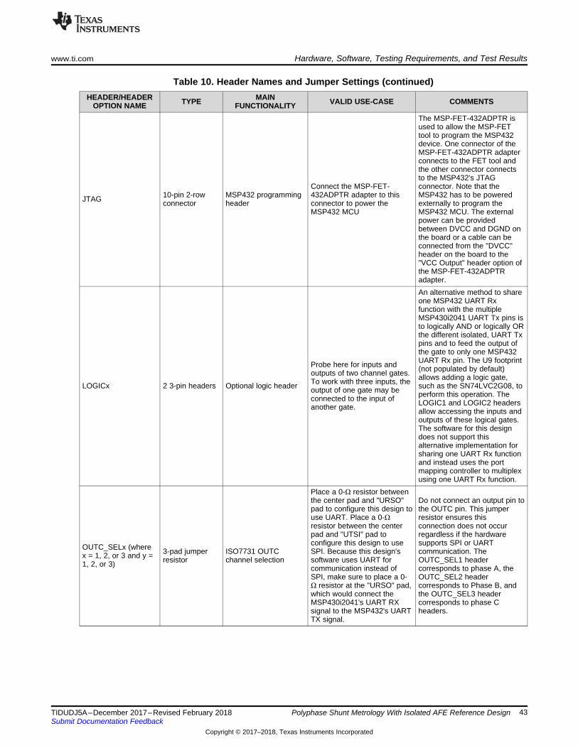
www.ti.com Hardware, Software, Testing Requirements, and Test Results
43TIDUDJ5A–December 2017–Revised February 2018Submit Documentation Feedback
Copyright © 2017–2018, Texas Instruments Incorporated
Polyphase Shunt Metrology With Isolated AFE Reference Design
Table 10. Header Names and Jumper Settings (continued)HEADER/HEADER
OPTION NAME TYPE MAINFUNCTIONALITY VALID USE-CASE COMMENTS
JTAG 10-pin 2-rowconnector
MSP432 programmingheader
Connect the MSP-FET-432ADPTR adapter to thisconnector to power theMSP432 MCU
The MSP-FET-432ADPTR isused to allow the MSP-FETtool to program the MSP432device. One connector of theMSP-FET-432ADPTR adapterconnects to the FET tool andthe other connector connectsto the MSP432's JTAGconnector. Note that theMSP432 has to be poweredexternally to program theMSP432 MCU. The externalpower can be providedbetween DVCC and DGND onthe board or a cable can beconnected from the "DVCC"header on the board to the"VCC Output" header option ofthe MSP-FET-432ADPTRadapter.
LOGICx 2 3-pin headers Optional logic header
Probe here for inputs andoutputs of two channel gates.To work with three inputs, theoutput of one gate may beconnected to the input ofanother gate.
An alternative method to shareone MSP432 UART Rxfunction with the multipleMSP430i2041 UART Tx pins isto logically AND or logically ORthe different isolated, UART Txpins and to feed the output ofthe gate to only one MSP432UART Rx pin. The U9 footprint(not populated by default)allows adding a logic gate,such as the SN74LVC2G08, toperform this operation. TheLOGIC1 and LOGIC2 headersallow accessing the inputs andoutputs of these logical gates.The software for this designdoes not support thisalternative implementation forsharing one UART Rx functionand instead uses the portmapping controller to multiplexusing one UART Rx function.
OUTC_SELx (wherex = 1, 2, or 3 and y =1, 2, or 3)
3-pad jumperresistor
ISO7731 OUTCchannel selection
Place a 0-Ω resistor betweenthe center pad and "URSO"pad to configure this design touse UART. Place a 0-Ωresistor between the centerpad and "UTSI" pad toconfigure this design to useSPI. Because this design'ssoftware uses UART forcommunication instead ofSPI, make sure to place a 0-Ω resistor at the "URSO" pad,which would connect theMSP430i2041's UART RXsignal to the MSP432's UARTTX signal.
Do not connect an output pin tothe OUTC pin. This jumperresistor ensures thisconnection does not occurregardless if the hardwaresupports SPI or UARTcommunication. TheOUTC_SEL1 headercorresponds to phase A, theOUTC_SEL2 headercorresponds to Phase B, andthe OUTC_SEL3 headercorresponds to phase Cheaders.
Hardware, Software, Testing Requirements, and Test Results www.ti.com
44 TIDUDJ5A–December 2017–Revised February 2018Submit Documentation Feedback
Copyright © 2017–2018, Texas Instruments Incorporated
Polyphase Shunt Metrology With Isolated AFE Reference Design
Table 10. Header Names and Jumper Settings (continued)HEADER/HEADER
OPTION NAME TYPE MAINFUNCTIONALITY VALID USE-CASE COMMENTS
P7 4-pin header MSP432 P7.0, P7.1,P7.2 and P7.3 headers
Probe here for P7.0, P7.1,P7.2, and P7.3 GPIO pins.
The P7.0, P7.1, and P7.2headers are used for adjustingcontrast of the LCD. P7.3 is notused in this design. P7.3 is aport mappable GPIO pin somultiple functions can bebrought out to this pin. If moreport mappable GPIO pins areneeded, P7.0, P7.1, and P7.2can also be used by disablingthe LCD contrast controlfeature and removing resistorsR18, R17, R7, and R6 from theboard.
REACT 1-pin header Reactive energy pulsesProbe between here andground for cumulative three-phase reactive energy pulses
RS232_3.3 1-pin headerVoltage sourceharvested from RS-232line
Voltage source that is used topower the TRS3232E-Q1 andISO7321 for isolated RS-232communication. This voltagesource is harvested from theRS-232 line
RS232_GND 1-pin header Ground connection forthe isolated RS-232
Ground connection for theisolated RS-232 circuitry
RX_EN Jumper header RS-232 receive enablePlace a jumper here to enablereceiving characters usingRS-232
TX_EN Jumper header RS-232 transmitenable
Place a jumper here to enableRS-232 transmissions
www.ti.com Hardware, Software, Testing Requirements, and Test Results
45TIDUDJ5A–December 2017–Revised February 2018Submit Documentation Feedback
Copyright © 2017–2018, Texas Instruments Incorporated
Polyphase Shunt Metrology With Isolated AFE Reference Design
3.1.3 SoftwareThe software in this reference design consists of the metrology software that is loaded onto theMSP430i2041 as well as the host software loaded onto the MSP432P4111. The following sectiondiscusses how to get started with the software.
3.1.3.1 Loading Metrology Code Onto MSP430i2041 DevicesThe MSP430i2041 source code is developed in the IAR™ environment using the IAR compiler version6.x. Earlier versions of IAR cannot open the project files. When the project is loaded in IAR version 6.x orlater, the integrated development environment (IDE) prompts the user to create a backup. Click "YES" toproceed. There are three main parts to the energy metrology software:• The toolkit that contains a library of mostly mathematics routines• The metrology code that is used for calculating metrology parameters• The application code that is used for communication to the MSP432 host
Figure 22 shows the contents of the msp430-emeters-i2040 folder, which contains the IAR projects for theMSP430i2041.
Figure 22. Source Folder Structure
Within the emeter-app-i2041 folder in the emeter-app folder, the emeter-app-i2041.ewp projectcorresponds to the application code. Similarly, within the emeter-metrology-i2041 folder in the emeter-metrology folder, the emeter-metrology-i2041.ewp project corresponds to the portion of the code formetrology. Additionally, the folder emeter-toolkit-i2041 within the emeter-toolkit has the correspondingtoolkit project file emeter-toolkit-i2041.ewp. For first-time use, TI recommends that all three projects becompletely rebuild by performing the following steps:1. Open the IAR IDE.2. Open the emeter-i2040 workspace, which is located in the Source folder.3. Within IAR workspace window, click the Overview tab to have a list view of all the projects.4. Right-click the emeter-toolkit-i2041 option in the workspace window and select Rebuild All, as
Figure 23 shows.5. Right-click the emeter-metrology-i2041 option in the workspace window and select Rebuild All, as
Figure 24 shows.6. Within IARs workspace window, click the emeter-app-i2041 tab.7. Within the workspace window, select emeter-app-i2041, click Rebuild All as Figure 25 shows, and then
download this project onto the MSP430i2041 device.

Hardware, Software, Testing Requirements, and Test Results www.ti.com
46 TIDUDJ5A–December 2017–Revised February 2018Submit Documentation Feedback
Copyright © 2017–2018, Texas Instruments Incorporated
Polyphase Shunt Metrology With Isolated AFE Reference Design
Note that if any changes are made to any of the files in the toolkit project and the project is compiled, themetrology project must be recompiled. After recompiling the metrology project, the application project mustthen be recompiled. Similarly, if any changes are made to any of the files in the metrology project and theproject is compiled, the application project must then be recompiled.
Figure 23. Toolkit Project Compilation Figure 24. Metrology Project Compilation
Figure 25. Application Project Compilation
After an executable file has been created, multiple MSP430i2041 devices can also be programmedsimultaneously using the MSP-Gang production programmer.

www.ti.com Hardware, Software, Testing Requirements, and Test Results
47TIDUDJ5A–December 2017–Revised February 2018Submit Documentation Feedback
Copyright © 2017–2018, Texas Instruments Incorporated
Polyphase Shunt Metrology With Isolated AFE Reference Design
3.1.3.2 Loading Metrology Code Onto MSP432P4111The MSP432 code is developed with Code Composer Studio™ (CCS) Version: 7.2.0.00013. To load thisfirmware onto the MSP432 MCU after installing CCS, follow these instructions:1. Download the SimpleLink MSP432 SDK available at http://www.ti.com/tool/simplelink-msp432-sdk.2. Open CCS.3. From the CCS menu bar, click File and select Import.4. From the import dialog box, expand the Code Composer Studio folder, select CCS Projects, then press
the Next button.5. Make sure the Select search-directory radio button is pressed and then press the Browse button next
to this button.6. Navigate and select the directory where the design's firmware is located.7. Select the discovered projects in the Discovered projects region of the window and click Finish.8. Select the design's projects in Project Explorer.9. Compile the projects by clicking Project from the menu bar and then clicking Build Project for each
project.10. The project settings are configured so that the MSP-FET debugger and MSP-FET-432ADPTR adapter
combination are the default options to program the MSP432P4111. If another debugger is used toprogram the MSP432 device, update the project settings accordingly to use this other debugger.
11. Load the program onto the MSP432 by clicking Run from the menu bard and then clicking Debug.
3.1.3.3 metrology-settings.hThe metrology-settings.h file contains different options for configuring the MSP432's metrology settings.Some of these options include the following:• TWO_ISOLATION_CHANNELS: This macro determines whether the MSP432 MCU is configured in
two-channel mode or three-channel mode. In two-channel mode, the MSP432's UART RX functionalityfor a phase is shared with the DRDY functionality of that phase so that only two isolation channels areused. In three-channel mode, the DRDY functionality and UART RX functionality are done on differentpins so there are three channels that are necessary. By defining this macro, the MSP432P4111 isconfigured in two channel mode. By not defining this macro, the MSP432 device is configured in threechannel mode. Both the MSP430i2041 devices and MSP432 MCU must have the same settings onwhether this macro is defined. If TWO_ISOLATION_CHANNELS is defined in the MSP432'smetrology-settings.h, then TWO_ISOLATION_CHANNELS must also be defined in the emeter-template.h file in the MSP430i2041 project. If TWO_ISOLATION_CHANNELS is not defined in theMSP432's metrology-settings.h, then TWO_ISOLATION_CHANNELS must also not be defined in theemeter-template.h file in the MSP430i2041 project.
• RESIDUAL_POWER_CUTOFF: Tiny power levels must not record energy at all, as they can just berounding errors, noise, or the consumption of the meter itself. This value is the cutoff level in milliwatts(this is the cutoff per phase). If the absolute value of power for a phase is below this threshold, thenthe phase would not output energy pulses and the energy buffers also will not be updated. In addition,that phase will not contribute to the cumulative active energy reading used to output energy pulses andupdate the energy buffers. Note that even if the absolute value of a phase's power is smaller thanRESIDUAL_POWER_CUTOFF, the active power readings would not get zeroed out. This macro onlyoperates on the energy readings.
• TOTAL_RESIDUAL_POWER_CUTOFF: Tiny power levels must not record energy at all, as they canjust be rounding errors, noise, or the consumption of the meter itself. This value is the cutoff level inmilliwatts (this is the cutoff per phase). If the absolute value of the cumulative power is below thisthreshold, then cumulative energy pulses will not be output and the energy buffers also will not beupdated. Note that even if the absolute value of cumulative power is smaller thanTOTAL_RESIDUAL_POWER_CUTOFF, the active power readings would not get zeroed out. Thismacro only operates on the energy readings.

Hardware, Software, Testing Requirements, and Test Results www.ti.com
48 TIDUDJ5A–December 2017–Revised February 2018Submit Documentation Feedback
Copyright © 2017–2018, Texas Instruments Incorporated
Polyphase Shunt Metrology With Isolated AFE Reference Design
• INTERRUPTION_THRESHOLD: A voltage interruption state is defined when a voltage that is 1 Vsmaller than this macro value divided by 1000 (that is, if the voltage in volts is smaller than((INTERRUPTION_THRESHOLD/1000)-1). The state exits the voltage interruption state when thevoltage is greater than 1 V larger than this macro divided by 1000 (that is, the voltage in volts is largerthan ((INTERRUPTION_THRESHOLD/1000)+1). This macro is used to determine when to sync againto find the new phase sequence after there is a voltage interruption.
• ACTIVE_ENERGY_PULSES_PER_KW_HOUR: This macro defines the total number of pulses per 1kWh of active energy at each phase. In this application, individual phase energy pulse generation isdisabled so this macro is disabled.
• REACTIVE_ENERGY_PULSES_PER_KVAR_HOUR: This macro defines the total number of pulsesper 1 kilovar of reactive energy at each phase. In this application, individual phase energy pulsegeneration is disabled so this macro is disabled.
• APPARENT_ENERGY_PULSES_PER_KVA_HOUR: This macro defines the total number of pulsesper 1 kVA of apparent energy at each phase. In this application, individual phase energy pulsegeneration is disabled so this macro is disabled.
• TOTAL_ACTIVE_ENERGY_PULSES_PER_KW_HOUR: This sets the number of pulses per kilo-watthour the meter will produce at its total active energy pulse. It does not affect the energy accumulationprocess. The default setting for this macro is 6400.
• TOTAL_REACTIVE_ENERGY_PULSES_PER_KVAR_HOUR: This sets the number of pulses perkilovar hour the meter will produce at its total reactive energy pulse. It does not affect the energyaccumulation process. The default setting for this macro is 6400.
• TOTAL_APPARENT_ENERGY_PULSES_PER_KVA_HOUR: This sets the number of pulses per kVAhour the meter will produce at its total apparent energy pulse. It does not affect the energyaccumulation process. Apparent energy pulse generation is disabled in the code, so this macro isdisabled.
• ENERGY_PULSE_DURATION: The duration of the LED on time for an energy pulse. This is measuredin timer interrupts (that is, increments 1/4000 s). The maximum allowed is 255, giving a pulse ofapproximately 64 ms. The default value for this macro is 20. For higher pulses/kWh constants, thevalue for this macro may need to be reduced.
• ACTIVE_ENERGY_SUPPORT: This switch selects support for measuring the active energyconsumption on a phase by phase basis. This will allow the GUI to display each phase's active energyconsumption in kWh.
• REACTIVE_ENERGY_SUPPORT: This switch selects support for measuring the reactive energyconsumption on a phase by phase basis. This will allow the GUI to display each phase's reactiveenergy consumption in kvarh.
• APPARENT_ENERGY_SUPPORT: This switch selects support for measuring the apparent energyconsumption on a phase by phase basis. This will allow the GUI to display each phase's apparentenergy consumption in kVA.
• TOTAL_ACTIVE_ENERGY_SUPPORT: This switch selects support for measuring the total activeenergy consumption. This will allow the GUI to display the cumulative phase's active energyconsumption in kWh. This is disabled for the neutral-monitoring configuration.
• TOTAL_REACTIVE_ENERGY_SUPPORT: This switch selects support for measuring the total reactiveenergy consumption. This will allow the GUI to display the cumulative phase's reactive energyconsumption in kvarh. This is disabled for the neutral-monitoring configuration.
• TOTAL_APPARENT_ENERGY_SUPPORT: This switch selects support for measuring the totalapparent energy consumption. This will allow the GUI to display the cumulative phase's apparentenergy consumption in kVA. This is disabled for the neutral-monitoring configuration.

www.ti.com Hardware, Software, Testing Requirements, and Test Results
49TIDUDJ5A–December 2017–Revised February 2018Submit Documentation Feedback
Copyright © 2017–2018, Texas Instruments Incorporated
Polyphase Shunt Metrology With Isolated AFE Reference Design
3.2 Testing and Results
3.2.1 Test SetupTo test for metrology accuracy, a source generator was used to provide the voltages and currents to thesystem at the proper locations mentioned in Section 3.1.2.1. Additionally, a nominal voltage of 230 V,calibration current of 10 A, and nominal frequency of 50 Hz are used for each phase.
When the voltages and currents are applied to the system, the system outputs the cumulative activeenergy pulses and cumulative reactive energy pulses at a rate of 6400 pulses/kWh. This pulse output isfed into a reference meter (in the test equipment for this reference design, this pulse output is integrated inthe same equipment used for the source generator) that determines the energy % error based on theactual energy provided to the system and the measured energy as determined by the system’s active andreactive energy output pulse. In this reference design, cumulative active energy error testing, cumulativereactive energy error testing, and frequency variation testing are performed after performing energy gaincalibration, phase compensation, and energy offset calibration as described in Section 3.2.2.2.2.
For cumulative active energy error and cumulative reactive energy error testing, current is varied from 100mA to 80 A simultaneously at each phase. For cumulative active energy error testing, a phase shift of 0°,60°, and −60° is applied between the voltage and current channels. Based on the error from the activeenergy output pulse, a plot of active energy % error versus current is created for 0°, 60°, and –60° phaseshifts. For cumulative reactive energy error testing, a similar process is followed except that 30°, 60°,–30°, and –60° phase shifts are used and cumulative reactive energy error is plotted instead of cumulativeactive energy error. Another set of tests performed are frequency variation tests. For this test, thefrequency is varied by ±2 Hz from its 50-Hz nominal frequency. This test is conducted at 1 A and 10 A atphase shifts of 0°, 60°, and −60°. The resulting active energy error under these conditions are logged.
3.2.2 Viewing Metrology Readings and Calibration
3.2.2.1 Viewing Results from LCDThe LCD scrolls between metering parameters every two seconds. For each metering parameter that isdisplayed on the LCD, three items are usually displayed on the screen: a symbol used to denote thephase of the parameter, text to denote which parameter is being displayed, and the actual value of theparameter. The phase symbol is displayed at the top of the LCD and denoted by a triangle shape. Theorientation of the symbol determines the corresponding phase. Figure 26, Figure 27, and Figure 28 showthe mapping between the different orientations of the triangle and the phase descriptor:
Figure 26. Symbol for Phase A Figure 27. Symbol for Phase B Figure 28. Symbol for Phase C
Aggregate results (such as cumulative active and reactive power) and parameters that are independent ofphase (such as time and date) are denoted by clearing all of the phase symbols on the LCD.

Phase
Designation
Value
Hardware, Software, Testing Requirements, and Test Results www.ti.com
50 TIDUDJ5A–December 2017–Revised February 2018Submit Documentation Feedback
Copyright © 2017–2018, Texas Instruments Incorporated
Polyphase Shunt Metrology With Isolated AFE Reference Design
The bottom line of the LCD is used to denote the value of the parameter being displayed. The text todenote the parameter being shown displays on the top line of the LCD. Table 11 shows the differentmetering parameters that are displayed on the LCD and the associated units in which they are displayed.The designation column shows which characters correspond to which metering parameter.
Table 11. Displayed Parameters
PARAMETER NAME DESIGNATION UNITS COMMENTS
Active power Watt (W) This parameter is displayed for each phase. Theaggregate active power is also displayed.
Reactive power Volt-AmpereReactive (var)
This parameter is displayed for each phase. Theaggregate reactive power is also displayed.
Apparent power Volt-Ampere (VA) This parameter is displayed for each phase.
Power factor Constant between 0and 1 This parameter is displayed for each phase.
Voltage Volts (V) This parameter is displayed for each phase.
Current Amps (A) This parameter is displayed for each phase.
Frequency Hertz (Hz) This parameter is displayed for each phase.
Total consumed activeenergy kWh This parameter is displayed for each phase.
Total consumed reactiveenergy kVarh
This parameter is displayed for each phase. Thisdisplays the sum of the reactive energy inquadrant 1 and quadrant 4.
Time Hour:minute:secondThis parameter is only displayed when the sequenceof aggregate readings are displayed. This parameteris not displayed once per phase.
Date Year:month:dayThis parameter is only displayed when theaggregate readings are displayed. This parameter isnot displayed once per phase.
Figure 29 shows an example of phase B's measured frequency of 49.99 Hz displayed on the LCD.
Figure 29. LCD
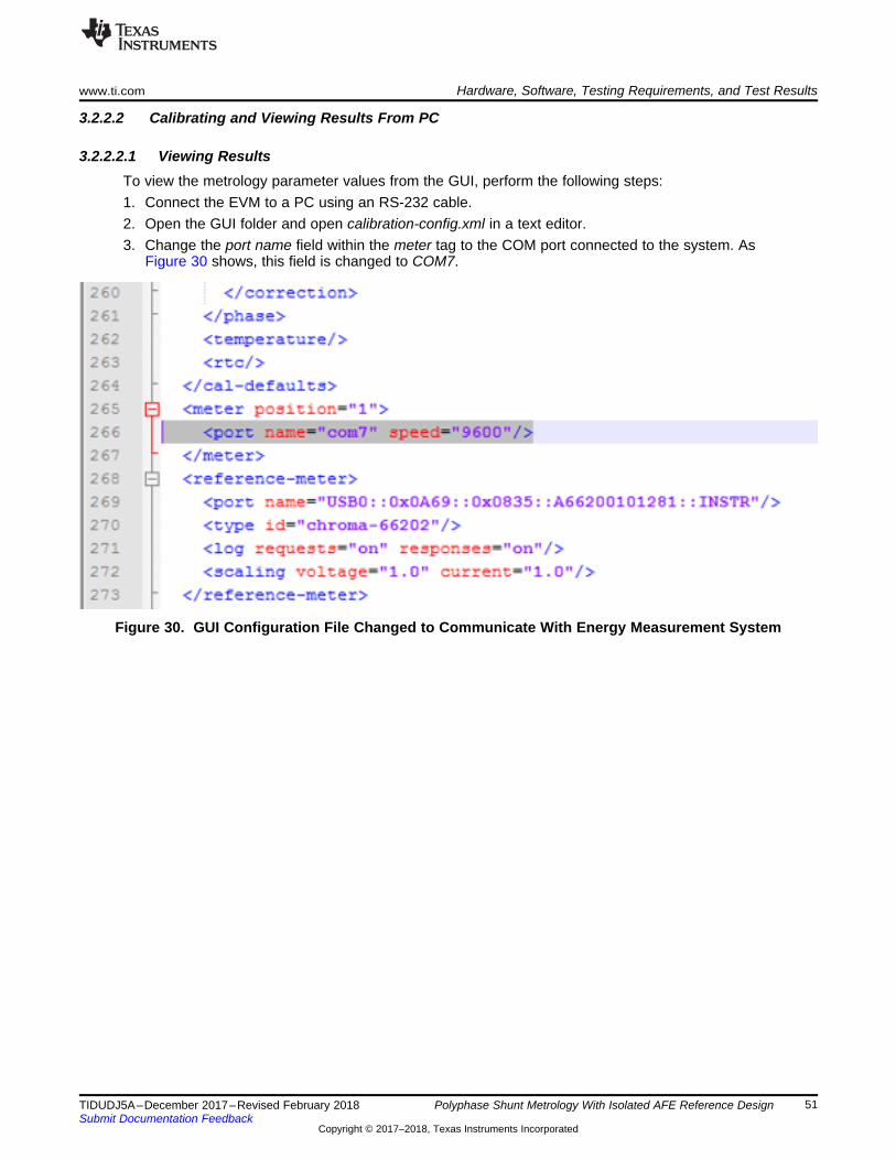
www.ti.com Hardware, Software, Testing Requirements, and Test Results
51TIDUDJ5A–December 2017–Revised February 2018Submit Documentation Feedback
Copyright © 2017–2018, Texas Instruments Incorporated
Polyphase Shunt Metrology With Isolated AFE Reference Design
3.2.2.2 Calibrating and Viewing Results From PC
3.2.2.2.1 Viewing ResultsTo view the metrology parameter values from the GUI, perform the following steps:1. Connect the EVM to a PC using an RS-232 cable.2. Open the GUI folder and open calibration-config.xml in a text editor.3. Change the port name field within the meter tag to the COM port connected to the system. As
Figure 30 shows, this field is changed to COM7.
Figure 30. GUI Configuration File Changed to Communicate With Energy Measurement System

Hardware, Software, Testing Requirements, and Test Results www.ti.com
52 TIDUDJ5A–December 2017–Revised February 2018Submit Documentation Feedback
Copyright © 2017–2018, Texas Instruments Incorporated
Polyphase Shunt Metrology With Isolated AFE Reference Design
4. Run the calibrator.exe file, which is located in the GUI folder. If the COM port in thecalibration-config.xml was changed in the previous step to the COM port connected to the EVM, theGUI opens (see Figure 31). If the GUI connects properly to the design, the top-left button is green. Ifthere are problems with connections or if the code is not configured correctly, the button is red. Clickthe green button to view the results.
Figure 31. GUI Startup Window
Upon clicking on the green button, the results window opens (see Figure 32). In the figure, there is atrailing "L" or "C" on the Power factor values to indicate an inductive or capacitive load, respectively. Inorder to get the Phase to Phase Sequence to work with the current version of the GUI, there were somechanges made that cause a couple misleading values to appear on the GUI. In the GUI, it displays afundamental active power of 0; however, note that the fundamental active power reading is not actuallytaken despite it being enabled in the GUI. In addition, the phase sequence is determined by looking at theorder of the "Phase to Phase" fields in the GUI for the different phases. The following combinations for thedifferent phase's "Phase to Phase" value corresponds to a phase ABC rotation, where Phase A is at 0°,Phase B is at 120°, and Phase C is at 240°:• 0.04° for Phase A, 0.00° for Phase B, 0.02° for Phase C (as shown in Figure 32)• 0.00° for Phase A, 0.02° for Phase B, 0.04° for Phase C• 0.02° for Phase A, 0.04° for Phase B, 0.00° for Phase C
When there is a CBA rotation, where Phase A is at 0°, Phase B is at 240°, and Phase C is at 120°, theGUI displays one of the three possible combinations for "Phase to Phase" readings:• 0.04° for Phase A, 0.02° for Phase B, 0.00° for Phase C• 0.00° for Phase A, 0.04° for Phase B, 0.02° for Phase C• 0.02° for Phase A, 0.00° for Phase B, 0.04° for Phase C
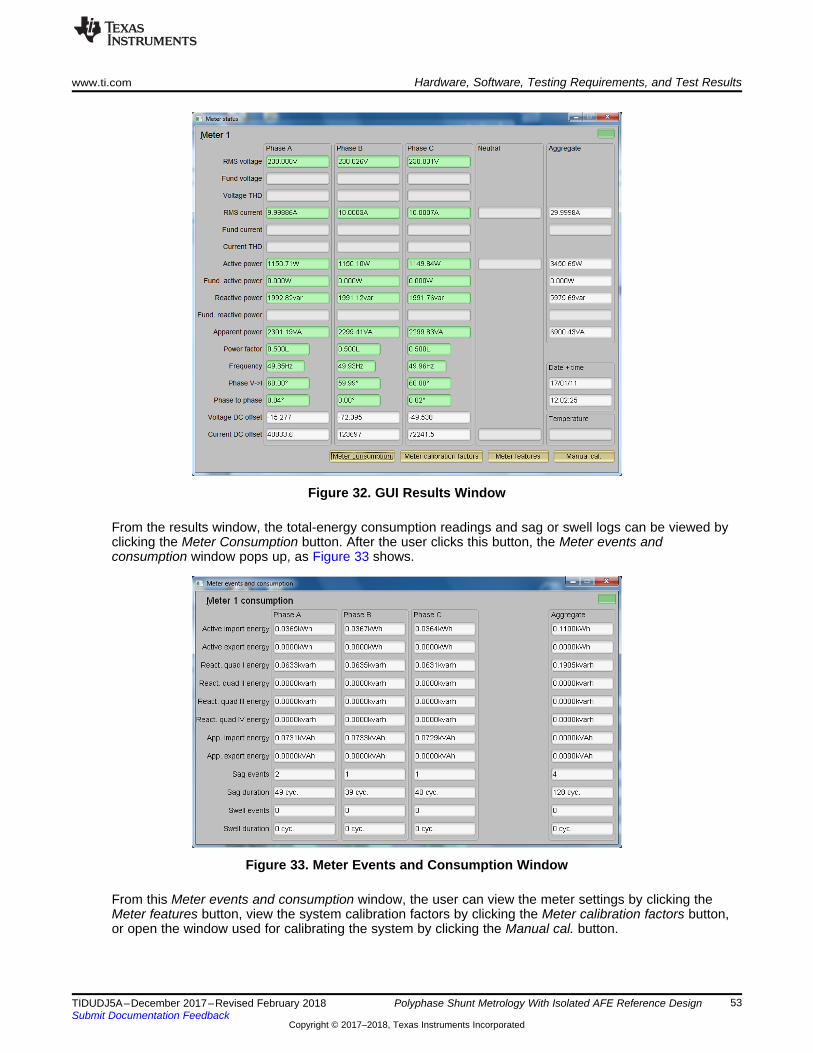
www.ti.com Hardware, Software, Testing Requirements, and Test Results
53TIDUDJ5A–December 2017–Revised February 2018Submit Documentation Feedback
Copyright © 2017–2018, Texas Instruments Incorporated
Polyphase Shunt Metrology With Isolated AFE Reference Design
Figure 32. GUI Results Window
From the results window, the total-energy consumption readings and sag or swell logs can be viewed byclicking the Meter Consumption button. After the user clicks this button, the Meter events andconsumption window pops up, as Figure 33 shows.
Figure 33. Meter Events and Consumption Window
From this Meter events and consumption window, the user can view the meter settings by clicking theMeter features button, view the system calibration factors by clicking the Meter calibration factors button,or open the window used for calibrating the system by clicking the Manual cal. button.

Hardware, Software, Testing Requirements, and Test Results www.ti.com
54 TIDUDJ5A–December 2017–Revised February 2018Submit Documentation Feedback
Copyright © 2017–2018, Texas Instruments Incorporated
Polyphase Shunt Metrology With Isolated AFE Reference Design
3.2.2.2.2 CalibrationCalibration is key to any meter performance, and it is absolutely necessary for every meter to go throughthis process. Initially, every meter exhibits different accuracies due to silicon-to-silicon differences, sensoraccuracies, and other passive tolerances. To nullify their effects, every meter must be calibrated. Toperform calibration accurately, there must be an accurate AC test source and a reference meter available.The source must be able to generate any desired voltage, current, and phase shifts (between V and I). Tocalculate errors in measurement, the reference meter acts as an interface between the source and themeter being calibrated. This section discusses a simple and effective method of calibration of this three-phase design.
The GUI used for viewing results can easily be used to calibrate the design. During calibration,parameters called calibration factors are modified in software to give the least error in measurement. Forthis meter, there are six main calibration factors for each phase: voltage scaling factor, active power offset(erroneously called voltage AC offset in the GUI), current scaling factor, reactive power offset (erroneouslycalled voltage AC offset in the GUI), power scaling factor, and the phase compensation factor. Thevoltage, current, and power scaling factors translate measured quantities in metrology software to real-world values represented in volts, amps, and watts, respectively. The last calibration factor is the phasecompensation factor, which is used to compensate any phase shifts introduced by the current sensors andother passives. Note that the voltage, current, and power calibration factors are independent of eachother. Therefore, calibrating voltage does not affect the readings for RMS current or power.
When the meter SW is flashed on the MSP430i2041 devices for the first time (available in the *.zip file),default calibration factors are loaded into these calibration factors. These values are to be modifiedthrough the GUI during calibration. The calibration factors are stored in INFO_MEM, and therefore, remainthe same if the meter is restarted.
Calibrating any of the scaling factors is referred to as gain correction. Calibrating the phase compensationfactors is referred to as phase correction. For the entire calibration process, the AC test source must beON, meter connections consistent with Section 3.1.2.1, and the energy pulses connected to the referencemeter.
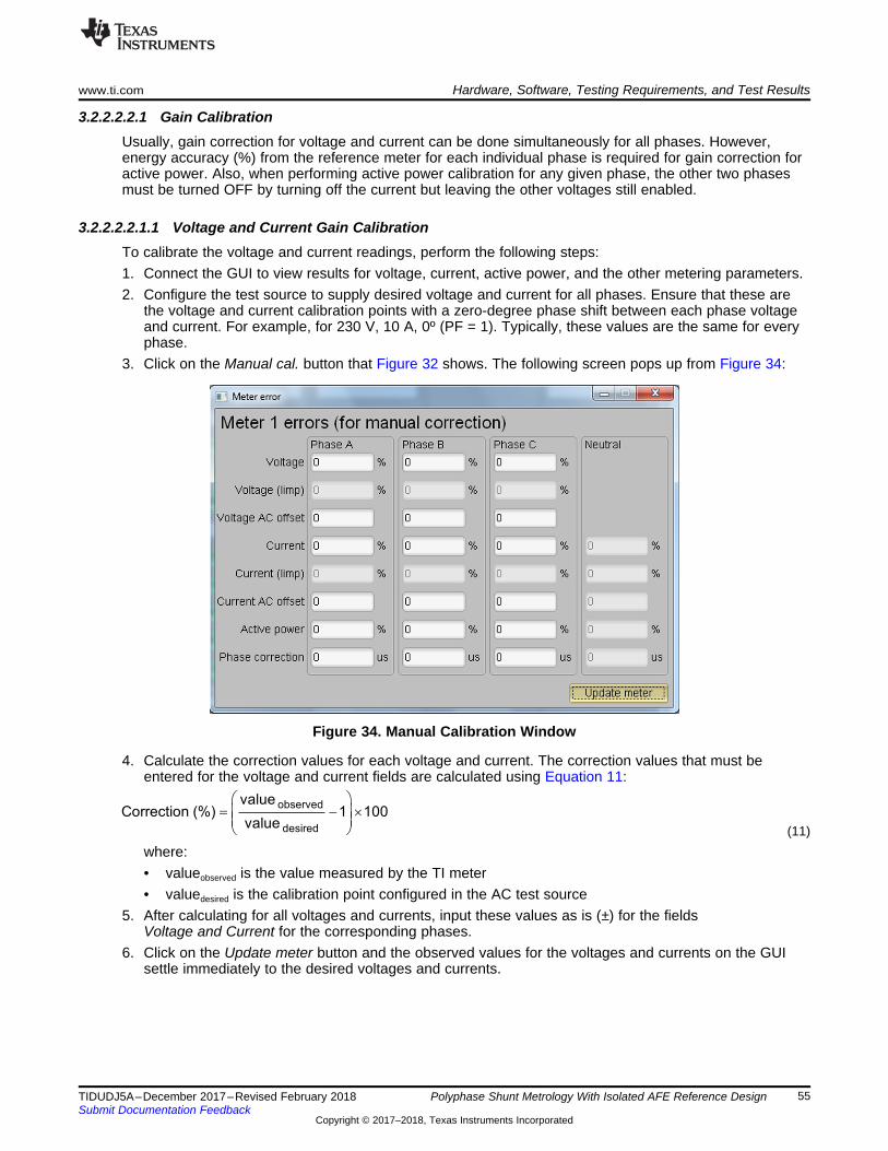
observed
desired
valueCorrection (%) 1 100
value
æ ö= - ´ç ÷
ç ÷è ø
www.ti.com Hardware, Software, Testing Requirements, and Test Results
55TIDUDJ5A–December 2017–Revised February 2018Submit Documentation Feedback
Copyright © 2017–2018, Texas Instruments Incorporated
Polyphase Shunt Metrology With Isolated AFE Reference Design
3.2.2.2.2.1 Gain CalibrationUsually, gain correction for voltage and current can be done simultaneously for all phases. However,energy accuracy (%) from the reference meter for each individual phase is required for gain correction foractive power. Also, when performing active power calibration for any given phase, the other two phasesmust be turned OFF by turning off the current but leaving the other voltages still enabled.
3.2.2.2.2.1.1 Voltage and Current Gain CalibrationTo calibrate the voltage and current readings, perform the following steps:1. Connect the GUI to view results for voltage, current, active power, and the other metering parameters.2. Configure the test source to supply desired voltage and current for all phases. Ensure that these are
the voltage and current calibration points with a zero-degree phase shift between each phase voltageand current. For example, for 230 V, 10 A, 0º (PF = 1). Typically, these values are the same for everyphase.
3. Click on the Manual cal. button that Figure 32 shows. The following screen pops up from Figure 34:
Figure 34. Manual Calibration Window
4. Calculate the correction values for each voltage and current. The correction values that must beentered for the voltage and current fields are calculated using Equation 11:
(11)where:• valueobserved is the value measured by the TI meter• valuedesired is the calibration point configured in the AC test source
5. After calculating for all voltages and currents, input these values as is (±) for the fieldsVoltage and Current for the corresponding phases.
6. Click on the Update meter button and the observed values for the voltages and currents on the GUIsettle immediately to the desired voltages and currents.

Hardware, Software, Testing Requirements, and Test Results www.ti.com
56 TIDUDJ5A–December 2017–Revised February 2018Submit Documentation Feedback
Copyright © 2017–2018, Texas Instruments Incorporated
Polyphase Shunt Metrology With Isolated AFE Reference Design
3.2.2.2.2.1.2 Active Power Gain Calibration
NOTE: This section is an example for one phase. Repeat these steps for other phases.
After performing gain correction for voltage and current, gain correction for active power must be done.Gain correction for active power is done differently in comparison to voltage and current. Although,conceptually, calculating using Step 4 with active power readings (displayed on the AC test source) canbe done, this method is not the most accurate and should be avoided.
The best option to get the Correction (%) is directly from the reference meters measurement error of theactive power. This error is obtained by feeding energy pulses to the reference meter. To perform activepower calibration, perform the following steps:1. Turn off the system and connect the energy pulse output of the system to the reference meter.
Configure the reference meter to measure the active power error based on these pulse inputs.2. Turn on the AC test source.3. Repeat Step 1 to Step 3 from Section 3.2.2.2.2.1.1 with the identical voltages, currents, and 0º phase
shift that were used in the same section.4. Obtain the % error in measurement from the reference meter. Note that this value may be negative.5. Enter the error obtained in Step 4 into the Active Power field under the corresponding phase in the GUI
window. This error is already the value and does not require calculation.6. Click the Update meter button and the error values on the reference meter immediately settle to a
value close to zero.
3.2.2.2.2.2 Phase CalibrationAfter performing power gain correction, phase calibration must be performed. Similar to active power gaincalibration, to perform phase correction on one phase, the other phases must be disabled. To performphase correction calibration, perform the following steps:1. If the AC test source has been turned OFF or reconfigured, perform Step 1 through Step 3 from
Section 3.2.2.2.2.1.1 using the identical voltages and currents used in that section.2. Disable all other phases that are not currently being calibrated by setting the current of these phases to
0 A.3. Modify only the phase-shift to a non-zero value; typically, +60º is chosen. The reference meter now
displays a different % error for active power measurement. Note that this value may be negative.4. If the error from Step 3 is not close to zero, or is unacceptable, perform phase correction by following
these steps:a. Enter a value as an update for the Phase Correction field for the phase that is being calibrated.
Usually, a small ± integer must be entered to bring the error closer to zero. Additionally, for aphase shift greater than 0 (for example: +60º), a positive (negative) error requires a positive(negative) number as correction.
b. Click on the Update meter button and monitor the error values on the reference meter.c. If this measurement error (%) is not accurate enough, fine-tune by incrementing or decrementing
by a value of 1 based on Step 4a and Step 4b. Note that after a certain point, the fine-tuning onlyresults in the error oscillating on either side of zero. The value that has the smallest absolute errormust be selected.
d. Change the phase now to −60° and check if this error is still acceptable. Ideally, errors must besymmetric for same phase shift on lag and lead conditions.
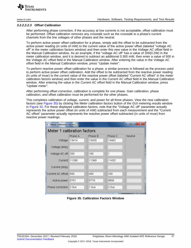
www.ti.com Hardware, Software, Testing Requirements, and Test Results
57TIDUDJ5A–December 2017–Revised February 2018Submit Documentation Feedback
Copyright © 2017–2018, Texas Instruments Incorporated
Polyphase Shunt Metrology With Isolated AFE Reference Design
3.2.2.2.2.3 Offset CalibrationAfter performing phase correction, if the accuracy at low currents is not acceptable, offset calibration mustbe performed. Offset calibration removes any crosstalk such as the crosstalk to a phase's currentchannels from the line voltages of other phases and the neutral.
To perform active power offset calibration for a phase, simply add the offset to be subtracted from theactive power reading (in units of mW) to the current value of the active power offset (labeled "voltage ACoff" in the meter calibration factors window) and then enter this new value in the Voltage AC offset field inthe Manual Calibration window. As an example, if the "voltage AC off" has a value of 200(0.2W) in themeter calibration window, and it is desired to subtract an additional 0.300 mW, then enter a value of 500 inthe Voltage AC offset field in the Manual Calibration window. After entering the value in the Voltage ACoffset field in the Manual Calibration window, press "Update meter".
To perform reactive power offset calibration for a phase, a similar process is followed as the process usedto perform active power offset calibration. Add the offset to be subtracted from the reactive power reading(in units of mvar) to the current value of the reactive power offset (labeled "Current AC offset" in the metercalibration factors window) and then enter the value in the Current AC offset field in the Manual Calibrationwindow. After entering the value in the Current AC offset field in the Manual Calibration window, press"Update meter".
After performing offset correction, calibration is complete for one phase. Gain calibration, phasecalibration, and offset calibration must be performed for the other phases.
This completes calibration of voltage, current, and power for all three phases. View the new calibrationfactors (see Figure 35) by clicking the Meter calibration factors button of the GUI metering results windowin Figure 32. For these displayed calibration factors, note that the "Voltage AC off" parameter actuallyrepresents the active power offset (in units of mW) subtracted from each measurement and the "CurrentAC offset" parameter actually represents the reactive power offset subtracted (in units of mvar) fromreactive power readings.
Figure 35. Calibration Factors Window
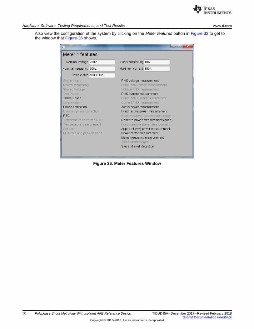
Hardware, Software, Testing Requirements, and Test Results www.ti.com
58 TIDUDJ5A–December 2017–Revised February 2018Submit Documentation Feedback
Copyright © 2017–2018, Texas Instruments Incorporated
Polyphase Shunt Metrology With Isolated AFE Reference Design
Also view the configuration of the system by clicking on the Meter features button in Figure 32 to get tothe window that Figure 36 shows.
Figure 36. Meter Features Window

Current (A)
Err
or (
%)
0 10 20 30 40 50 60 70 80-1
-0.8
-0.6
-0.4
-0.2
0
0.2
0.4
0.6
0.8
1
D001
0q60q-60q
www.ti.com Hardware, Software, Testing Requirements, and Test Results
59TIDUDJ5A–December 2017–Revised February 2018Submit Documentation Feedback
Copyright © 2017–2018, Texas Instruments Incorporated
Polyphase Shunt Metrology With Isolated AFE Reference Design
3.2.3 Test ResultsFor the following test results, gain, phase, and offset calibration are applied to the meter. At highercurrents, the % error shown is dominated by shunt resistance drift caused by the increased heatgenerated at high currents.
Table 12. Cumulative Active Energy % ErrorVersus Current, 400-µΩ Shunts
CURRENT (A) 0° 60° –60°0.1 –0.0095 0.1495 0.13
0.25 0.0027 0.025 0.02450.5 0.0115 –0.004 0.063
1 0.007 –0.031 –0.0022 –0.013 –0.024 –0.0025 –0.02 –0.023 0.003
10 –0.017 –0.032 –0.00220 –0.026 –0.049 –0.03930 –0.032 –0.06 –0.06740 –0.057 –0.097 –0.09950 –0.096 –0.149 –0.10960 –0.147 –0.205 –0.19470 –0.182 –0.253 –0.25180 –0.241 –0.3 –0.31
Figure 37. Cumulative Active Energy % Error Versus Current, 400-µΩ Shunts
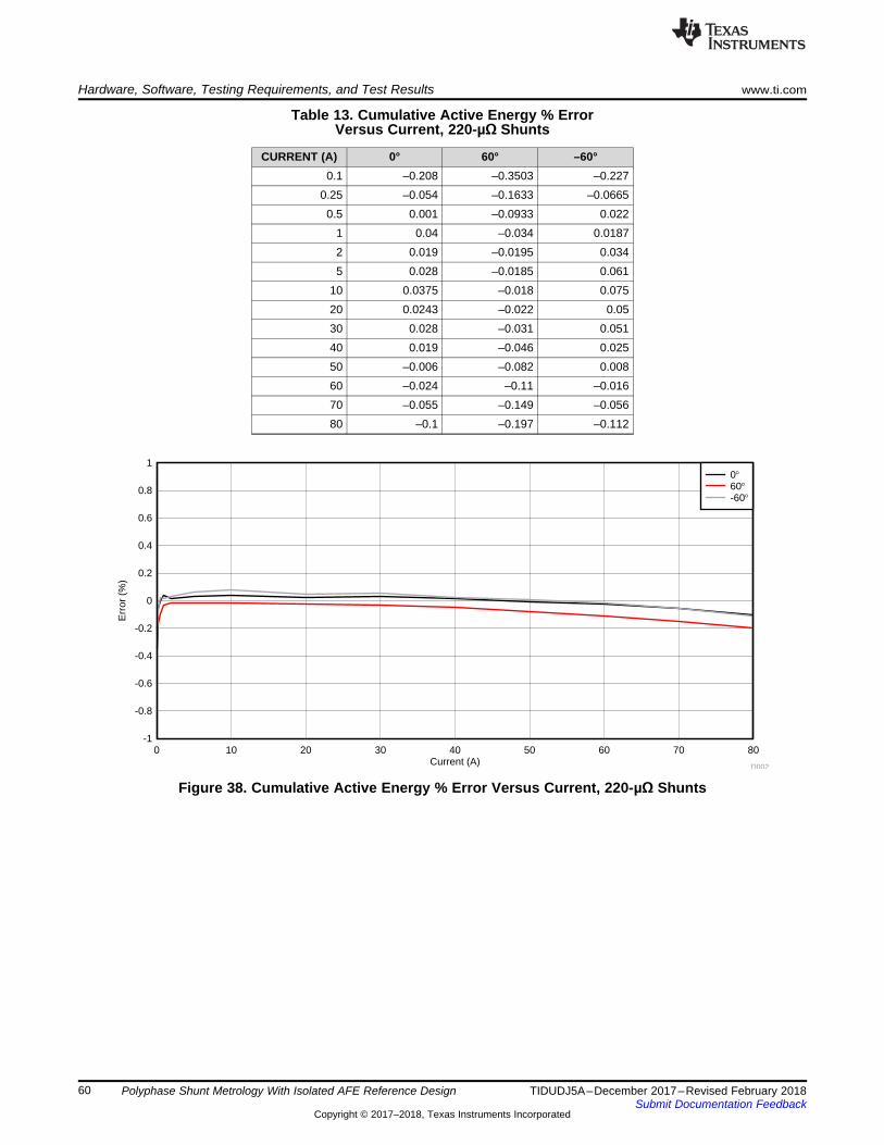
Current (A)
Err
or (
%)
0 10 20 30 40 50 60 70 80-1
-0.8
-0.6
-0.4
-0.2
0
0.2
0.4
0.6
0.8
1
D002
0q60q-60q
Hardware, Software, Testing Requirements, and Test Results www.ti.com
60 TIDUDJ5A–December 2017–Revised February 2018Submit Documentation Feedback
Copyright © 2017–2018, Texas Instruments Incorporated
Polyphase Shunt Metrology With Isolated AFE Reference Design
Table 13. Cumulative Active Energy % ErrorVersus Current, 220-µΩ Shunts
CURRENT (A) 0° 60° –60°0.1 –0.208 –0.3503 –0.227
0.25 –0.054 –0.1633 –0.06650.5 0.001 –0.0933 0.022
1 0.04 –0.034 0.01872 0.019 –0.0195 0.0345 0.028 –0.0185 0.061
10 0.0375 –0.018 0.07520 0.0243 –0.022 0.0530 0.028 –0.031 0.05140 0.019 –0.046 0.02550 –0.006 –0.082 0.00860 –0.024 –0.11 –0.01670 –0.055 –0.149 –0.05680 –0.1 –0.197 –0.112
Figure 38. Cumulative Active Energy % Error Versus Current, 220-µΩ Shunts

Current (A)
Y A
xis
Titl
e (U
nit)
0 10 20 30 40 50 60 70 80-1
-0.8
-0.6
-0.4
-0.2
0
0.2
0.4
0.6
0.8
1
D003
30q60q-30q-60q
www.ti.com Hardware, Software, Testing Requirements, and Test Results
61TIDUDJ5A–December 2017–Revised February 2018Submit Documentation Feedback
Copyright © 2017–2018, Texas Instruments Incorporated
Polyphase Shunt Metrology With Isolated AFE Reference Design
Table 14. Cumulative Reactive Energy % ErrorVersus Current
CURRENT (A) 30° 60° –30° –60°0.1 –0.1395 0.0215 0.023 0.0355
0.25 –0.1895 –0.1443 0.0917 0.08171 –0.0853 –0.0567 0.0063 –0.0035 –0.042 –0.0363 –0.015 –0.027
10 –0.0363 –0.0303 –0.019 –0.01630 –0.079 –0.07 –0.045 –0.0650 –0.091 –0.111 –0.099 –0.1280 –0.139 –0.17 –0.2 –0.22
Figure 39. Cumulative Reactive Energy % Error Versus Current
Table 15. Cumulative Active Energy Measurement ErrorVersus Frequency, ±2 Hz From Nominal Frequency
CONDITIONS 48 Hz 50 Hz 52 Hz1 A, 0° 0.022 0.0075 –0.0221 A, 60° 0.0057 –0.0173 –0.0241 A, 300° 0.01 0.006 –0.018310 A, 0° –0.0127 –0.0177 –0.026310 A, 60° –0.038 –0.029 –0.04110 A, 300° –0.028 –0.012 –0.02

Design Files www.ti.com
62 TIDUDJ5A–December 2017–Revised February 2018Submit Documentation Feedback
Copyright © 2017–2018, Texas Instruments Incorporated
Polyphase Shunt Metrology With Isolated AFE Reference Design
4 Design Files
4.1 SchematicsTo download the schematics, see the design files at TIDA-01550.
4.2 Bill of MaterialsTo download the bill of materials (BOM), see the design files at TIDA-01550.
4.3 PCB Layout RecommendationsFor this reference design, follow these general guidelines:• Place decoupling capacitors close to their associated pins.• Use ground planes instead of ground traces and minimize the cuts in the ground plane.• Give each MSP430i2041 device its own set of ground planes. Each of these ground planes is actually
referenced from a different line voltage because each MSP430i2041 device must be connected to adifferent line voltage.
• Be careful to avoid crosstalk on a phase from other phase voltages and the neutral.• For the MSP432P4111, minimize the length of the traces used to connect the crystal to the
microcontroller. Place guard rings around the leads of the crystal and ground the crystal housing. Inaddition, there must be clean ground underneath the crystal and placing any traces underneath thecrystal must be avoided. Also, keep high frequency signals away from the crystal.
• Use wide traces for power supply connections.• Maintain at least an 8.1-mm spacing between the ground planes of the MSP430i2041 device and the
MSP432P4111 ground planes. This spacing maintains the recommended clearance for the ISO7731isolation rating. In addition, ensure that the recommended clearance and creepage spacing for otherisolation devices (such as the ISO7720 and ISO7721) is also followed.
• Keep the traces of the analog input pin symmetrical and as close as possible to each other.
4.4 CAD ProjectTo download the CAD project files, see the design files at TIDA-01550.
4.5 Gerber FilesTo download the Gerber files, see the design files at TIDA-01550.
5 Software FilesTo download the software files, see the design files at TIDA-01550.
6 Related Documentation1. Texas Instruments, TIDA-00163 Self-Powered Isolated RS-232 to UART Interface Reference Design
6.1 TrademarksE2E, MSP432, MSP430, SimpleLink, Code Composer Studio are trademarks of Texas Instruments.Arm, Cortex are registered trademarks of Arm Limited (or its subsidiaries).Bluetooth is a registered trademark of Bluetooth SIG.IAR is a trademark of IAR Systems AB.Wi-Fi is a registered trademark of Wi-Fi Alliance.All other trademarks are the property of their respective owners.

www.ti.com About the Author
63TIDUDJ5A–December 2017–Revised February 2018Submit Documentation Feedback
Copyright © 2017–2018, Texas Instruments Incorporated
Polyphase Shunt Metrology With Isolated AFE Reference Design
7 About the AuthorMEKRE MESGANAW is a systems engineer in the Grid Infrastructure group at Texas Instruments, wherehe primarily works on grid monitoring and electricity metering customer support and reference designdevelopment. Mekre received his bachelor of science and master of science in computer engineering fromthe Georgia Institute of Technology.

Revision History www.ti.com
64 TIDUDJ5A–December 2017–Revised February 2018Submit Documentation Feedback
Copyright © 2017–2018, Texas Instruments Incorporated
Revision History
Revision HistoryNOTE: Page numbers for previous revisions may differ from page numbers in the current version.
Changes from Original (December 2017) to A Revision ................................................................................................ Page
• Changed isolation rating of DBQ package from 2500 VRMS to 3000 VRMS .......................................................... 6• Changed limit of galvanic isolation from 2.5 kVRMS to 3.0 kVRMS..................................................................... 8

IMPORTANT NOTICE FOR TI DESIGN INFORMATION AND RESOURCES
Texas Instruments Incorporated (‘TI”) technical, application or other design advice, services or information, including, but not limited to,reference designs and materials relating to evaluation modules, (collectively, “TI Resources”) are intended to assist designers who aredeveloping applications that incorporate TI products; by downloading, accessing or using any particular TI Resource in any way, you(individually or, if you are acting on behalf of a company, your company) agree to use it solely for this purpose and subject to the terms ofthis Notice.TI’s provision of TI Resources does not expand or otherwise alter TI’s applicable published warranties or warranty disclaimers for TIproducts, and no additional obligations or liabilities arise from TI providing such TI Resources. TI reserves the right to make corrections,enhancements, improvements and other changes to its TI Resources.You understand and agree that you remain responsible for using your independent analysis, evaluation and judgment in designing yourapplications and that you have full and exclusive responsibility to assure the safety of your applications and compliance of your applications(and of all TI products used in or for your applications) with all applicable regulations, laws and other applicable requirements. Yourepresent that, with respect to your applications, you have all the necessary expertise to create and implement safeguards that (1)anticipate dangerous consequences of failures, (2) monitor failures and their consequences, and (3) lessen the likelihood of failures thatmight cause harm and take appropriate actions. You agree that prior to using or distributing any applications that include TI products, youwill thoroughly test such applications and the functionality of such TI products as used in such applications. TI has not conducted anytesting other than that specifically described in the published documentation for a particular TI Resource.You are authorized to use, copy and modify any individual TI Resource only in connection with the development of applications that includethe TI product(s) identified in such TI Resource. NO OTHER LICENSE, EXPRESS OR IMPLIED, BY ESTOPPEL OR OTHERWISE TOANY OTHER TI INTELLECTUAL PROPERTY RIGHT, AND NO LICENSE TO ANY TECHNOLOGY OR INTELLECTUAL PROPERTYRIGHT OF TI OR ANY THIRD PARTY IS GRANTED HEREIN, including but not limited to any patent right, copyright, mask work right, orother intellectual property right relating to any combination, machine, or process in which TI products or services are used. Informationregarding or referencing third-party products or services does not constitute a license to use such products or services, or a warranty orendorsement thereof. Use of TI Resources may require a license from a third party under the patents or other intellectual property of thethird party, or a license from TI under the patents or other intellectual property of TI.TI RESOURCES ARE PROVIDED “AS IS” AND WITH ALL FAULTS. TI DISCLAIMS ALL OTHER WARRANTIES ORREPRESENTATIONS, EXPRESS OR IMPLIED, REGARDING TI RESOURCES OR USE THEREOF, INCLUDING BUT NOT LIMITED TOACCURACY OR COMPLETENESS, TITLE, ANY EPIDEMIC FAILURE WARRANTY AND ANY IMPLIED WARRANTIES OFMERCHANTABILITY, FITNESS FOR A PARTICULAR PURPOSE, AND NON-INFRINGEMENT OF ANY THIRD PARTY INTELLECTUALPROPERTY RIGHTS.TI SHALL NOT BE LIABLE FOR AND SHALL NOT DEFEND OR INDEMNIFY YOU AGAINST ANY CLAIM, INCLUDING BUT NOTLIMITED TO ANY INFRINGEMENT CLAIM THAT RELATES TO OR IS BASED ON ANY COMBINATION OF PRODUCTS EVEN IFDESCRIBED IN TI RESOURCES OR OTHERWISE. IN NO EVENT SHALL TI BE LIABLE FOR ANY ACTUAL, DIRECT, SPECIAL,COLLATERAL, INDIRECT, PUNITIVE, INCIDENTAL, CONSEQUENTIAL OR EXEMPLARY DAMAGES IN CONNECTION WITH ORARISING OUT OF TI RESOURCES OR USE THEREOF, AND REGARDLESS OF WHETHER TI HAS BEEN ADVISED OF THEPOSSIBILITY OF SUCH DAMAGES.You agree to fully indemnify TI and its representatives against any damages, costs, losses, and/or liabilities arising out of your non-compliance with the terms and provisions of this Notice.This Notice applies to TI Resources. Additional terms apply to the use and purchase of certain types of materials, TI products and services.These include; without limitation, TI’s standard terms for semiconductor products http://www.ti.com/sc/docs/stdterms.htm), evaluationmodules, and samples (http://www.ti.com/sc/docs/sampterms.htm).
Mailing Address: Texas Instruments, Post Office Box 655303, Dallas, Texas 75265Copyright © 2018, Texas Instruments Incorporated