Polymer Materials for Microlithography
17
Chem.Rev.1989, 89, 1273-1289 1273 Polymer Materials for Microlithography Contents E. REICHMANIS’ and L. F. THOMPSON* AT&T Bell Laboratories, Murray Hill, New Jersey 07974 Received January 20, 1989 (Revised Manuscript Received March 22, 1989) ance of the different resist systems are reviewed. Introduction Short-Wavelength Photolithography X-ray Lithography Electron Beam Lithography Scanning Ion Beam Lithography Summary Negative Resists Positive Resists Single-Level Resist Chemistry Chain Scission Resists Solution Inhibition Resists Nonconventional Resist Chemistry Multilevel Resist Chemistry Multilevel Resist Processes Employing Reactive Ion Etching Pattern-Transfer Techniques Gas-Phase Functionalization Conclusion 1273 1275 1275 1275 1275 1276 1276 1276 1278 1278 1279 1281 1283 1284 1286 1287 Overview Astonishing progress has been made in very large scale integrated (VLSI) electronic devices in the past decade. These advances are placing increasing demands on microlithography, the technology used to generate the high-resolution circuit elements characteristic of today’s integrated circuits. In 1976, state-of-the-art devices contained a few thousand transistors with minimum features of 5-6 pm. In comparison, today’s devices contain over 1 million transistors and minimum features of 0.9 pm. Within the next 10-15 years, some new form of lithography will be required with a capa- bility of routinely producing features of <5 pm. The alternatives to conventional photolithography are short-wavelength photolithography, scanning electron beam lithography, X-ray lithography, and scanning ion beam lithography. No matter which of those technol- ogies becomes dominant, new resists and processes will be required. In addition, the necessity to accommodate the effect of topographical features on the wafer surface that is exacerbated by the continuous decrease in fea- ture size will demand some form of “multilevel”scheme. In the simplest multilevel scheme, resist is required to function as both a radiation-sensitive imaging material and a pattern-transfer mask for the reactive ion etching of the thick planarizing layer. This review describes the new chemistries and approaches that have been recently published for alternate lithographic strategies. Con- siderable attention is devoted to metal-containing polymers that are useful in multilevel applications. For each system, the chemistry and lithographic perform- OOO9-2665/89/0789-1273$08.50/0 Introductlon Astonishing progress has been made in microelec- tronics, especially in the technology of lithography used to generate the high-resolution circuit elements char- acteristic of today’s integrated circuits.’ In 1976, the state-of-the-art dynamic random access memory (DRAM) device was capable of storing 4000 bits of data and had 5-6-pm minimum features. These devices were patterned by photolithography using either contact printing or, the then relatively new, 1:l projection printing. Today, devices with one million bits of storage capacity are commercially available with minimum features of 0.9 pm.2 Surprisingly, photolithography is still the technology used to fabricate microelectronic chips. Step-and-repeat 5X or lox reduction cameras or highly sophisticated 1:l projection printers are the dominant printing tools. There is perhaps no better example than lithography to illustrate the uncertainty associated with predicting technological direction and change. In 1976, it was generally believed (albeit not by everyone) that photolithography would not be able to produce features smaller than ca. 1.5-2.0 pm with high chip yields in a production environment. The current belief is that conventional photolithography will be able to print features as small as 0.5 pm and will remain the dominant technology well into the first half of the 19%. The same basic positive photoresist based on a diazonaphthoquinone photoactive compound and novolac resin that has been in pervasive use since the mid-1970s will likely still be the resist of choice. The cost of introducing a new technology and the cost as- sociated with development and implementation of new hardware and resist materials are strong driving forces pushing photolithography to its absolute resolution limit and extending its commercial viability. The technological alternatives to conventional pho- tolithography are largely the Same as they were a decade ago, i.e., short-wavelength photolithography, scanning electron beam lithography, X-ray lithography, or scan- ning ion beam lith~graphy.~?~ It is not the intent of this review to discuss the various lithographic technologies in detail; however, each will be briefly summarized so that the resist chemistry can be better appreciated. No matter which technology becomes dominant after photolithography has reached its limit, new resists and processes will be required, necessitating enormous in- vestment in research and process development. The introduction of new resist materials and processes will also require a considerable lead time, probably in excess of 3-6 years, to bring them to the performance level 0 1989 American Chemical Society
-
Upload
devendratiwari0 -
Category
Documents
-
view
57 -
download
2
Transcript of Polymer Materials for Microlithography

Chem.Rev.1989, 89 , 1273-1289 1273
Polymer Materials for Microlithography
Contents
E. REICHMANIS’ and L. F. THOMPSON*
AT&T Bell Laboratories, Murray Hill, New Jersey 07974
Received January 20, 1989 (Revised Manuscript Received March 22, 1989)
ance of the different resist systems are reviewed.
Introduction Short-Wavelength Photolithography X-ray Lithography Electron Beam Lithography Scanning Ion Beam Lithography Summary
Negative Resists Positive Resists
Single-Level Resist Chemistry
Chain Scission Resists Solution Inhibition Resists
Nonconventional Resist Chemistry Multilevel Resist Chemistry
Multilevel Resist Processes Employing Reactive Ion Etching Pattern-Transfer Techniques
Gas-Phase Functionalization Conclusion
1273 1275 1275 1275 1275 1276 1276 1276 1278 1278 1279 1281 1283 1284
1286 1287
Overview
Astonishing progress has been made in very large scale integrated (VLSI) electronic devices in the past decade. These advances are placing increasing demands on microlithography, the technology used to generate the high-resolution circuit elements characteristic of today’s integrated circuits. In 1976, state-of-the-art devices contained a few thousand transistors with minimum features of 5-6 pm. In comparison, today’s devices contain over 1 million transistors and minimum features of 0.9 pm. Within the next 10-15 years, some new form of lithography will be required with a capa- bility of routinely producing features of <5 pm. The alternatives to conventional photolithography are short-wavelength photolithography, scanning electron beam lithography, X-ray lithography, and scanning ion beam lithography. No matter which of those technol- ogies becomes dominant, new resists and processes will be required. In addition, the necessity to accommodate the effect of topographical features on the wafer surface that is exacerbated by the continuous decrease in fea- ture size wil l demand some form of “multilevel” scheme. In the simplest multilevel scheme, resist is required to function as both a radiation-sensitive imaging material and a pattern-transfer mask for the reactive ion etching of the thick planarizing layer. This review describes the new chemistries and approaches that have been recently published for alternate lithographic strategies. Con- siderable attention is devoted to metal-containing polymers that are useful in multilevel applications. For each system, the chemistry and lithographic perform-
OOO9-2665/89/0789-1273$08.50/0
Introductlon Astonishing progress has been made in microelec-
tronics, especially in the technology of lithography used to generate the high-resolution circuit elements char- acteristic of today’s integrated circuits.’ In 1976, the state-of-the-art dynamic random access memory (DRAM) device was capable of storing 4000 bits of data and had 5-6-pm minimum features. These devices were patterned by photolithography using either contact printing or, the then relatively new, 1:l projection printing. Today, devices with one million bits of storage capacity are commercially available with minimum features of 0.9 pm.2 Surprisingly, photolithography is still the technology used to fabricate microelectronic chips. Step-and-repeat 5X or lox reduction cameras or highly sophisticated 1:l projection printers are the dominant printing tools. There is perhaps no better example than lithography to illustrate the uncertainty associated with predicting technological direction and change. In 1976, it was generally believed (albeit not by everyone) that photolithography would not be able to produce features smaller than ca. 1.5-2.0 pm with high chip yields in a production environment. The current belief is that conventional photolithography will be able to print features as small as 0.5 pm and will remain the dominant technology well into the first half of the 19%. The same basic positive photoresist based on a diazonaphthoquinone photoactive compound and novolac resin that has been in pervasive use since the mid-1970s will likely still be the resist of choice. The cost of introducing a new technology and the cost as- sociated with development and implementation of new hardware and resist materials are strong driving forces pushing photolithography to its absolute resolution limit and extending its commercial viability.
The technological alternatives to conventional pho- tolithography are largely the Same as they were a decade ago, i.e., short-wavelength photolithography, scanning electron beam lithography, X-ray lithography, or scan- ning ion beam li th~graphy.~?~ It is not the intent of this review to discuss the various lithographic technologies in detail; however, each will be briefly summarized so that the resist chemistry can be better appreciated. No matter which technology becomes dominant after photolithography has reached its limit, new resists and processes will be required, necessitating enormous in- vestment in research and process development. The introduction of new resist materials and processes will also require a considerable lead time, probably in excess of 3-6 years, to bring them to the performance level
0 1989 American Chemical Society

Reichmanis and Thompson 1274 Chemical Reviews. 1989. Voi. 89. No. 6
Elsa Relchmanls is Supervisor of the Radiation Sensitive Materials and Applications Group at AT8T Bell Laboratories, Murray Hill, NJ. She received her Ph.D. (1975) and B.S. (1972) degrees in chew istry from Syracuse University and joined Bell Laboratories in 1978 atter completing a Chaim Weizmann Postdoctoral Fellowship pro- gram. Her research interests include tm chemistry. proper6es. and applications of radiation-sensitive materials, particularly as they relate to resists and other materials for lithographic applications. Other interests include plasma chemistry of organic and organo- metallic systems. polymer chemistry, and organic and polymer photochemistry. h. Reichmanis has published in a variety of arms of chemistry ranging from synthetic organic and heteroaromatic chemistry to radiation chemistry of polymeric systems. She has numerous publications in the area of resist materials and is the holder of several patents.
Law F. Thompson, Head, Organic Materials and Chemical EngC neering, ATBT Bell Laboratories (1980 to present), received his Ph.D. in Chemistry in 1971 from the University of Missouri-Rolla. and his B.S. and M.S. degrees from Tennessee Technological Univerrity, Cookeville, TN. During his industrial career at AT8T Bell Laboratories. which began when he became a Member of Tech- nical Staff in 1971, he has been involved in the synthesis. char- acterization, and process development of polymer materials used in the manufacture of intqrated circuits and chemical processing for semiconductor and optical fiber manufacturing. This work has resuiied in over 60 publications. 50 invited talks, and 14 US. Patents. His major contributions include the development of COP, PBS. GMC. and NPR electron beam resists. and recently he has been working on materials for deep-UV and X-ray resist appiica- tions. He has bean involved in process design of purification and recovery systems used in optical fiber manufacture. He is active in the American Chemical Society and the American Institute of Chemical Engineers. He is a member of the Society of Photo- graphic Instrumentation Engineers. the Electrochemical Society, The American Vacuum Society, and the IEEE. He is a member of the Council of Chemical Research and a member of the Chemical Engineering Survey Committee of the National Research Council
currently realized by conventional positive photoresists. A modern integrated circuit is a complex three-di-
mensional structure of alternating, patterned layers of
EXPOSING
EXPOSURE
I DEVELOPING
POSITIVE RESIST NEGATITIVE RESlST / \
ETCHING 4ND STRlPPlNG
r 3 I Figure I. Schematic of the lithographic process.'
Loo D - Figure 2. Representative contrast curves for (a) poeitive resista and (h) negative resists.
conductors, dielectrics, and semiconductor films. Th is structure i s fabricated on an ul t rahigh-pur i ty wafer substrate of a semiconducting material such as silicon. T h e performance o f the device is t o a large degree governed by the size of the ind iv idual elements. As a general rule, the smaller the elements, the higher the device performance. T h e device structure is produced by a series of steps used to precisely pat tem each layer. T h e pattems are formed by lithographic processes that consist of two steps: (1) delineation o f the patterns in a radiation-sensitive thin-polymer film, and (2) transfer of that pattern w i t h an appropriate etching technique. A schematic representation of the lithographic process i s shown in Figure 1.
The focus of th is review concerns the design and se- lection o f polymer materials tha t are useful as radia- tion-sensitive resist films. Such polymers mus t be carefully designed to meet the specific requirements of each lithographic technology and device process. Al- though these requirements vary according to the ra-
Polymer Materlals for Microlithography
diation source and device process requirements, the following are ubiquitous: sensitivity, contrast, etching resistance, shelf life, and purity. These properties can be achieved by careful manipulation of the polymer structure and molecular properties.
Resists function by altering their solubility through radiation-induced chemical reactions. These reactions can either increase the solubility (positive tone) or de- crease the solubility (negative tone) of the irradiated region. The terms positive and negative resists reflect this change in solubility.
Sensitivity and contrast of a resist are determined by measuring the change in solubility as a function of the radiation dose received by the polymer. Although these two parameters are dependent on many variables such as developer strength, photon or particle energy, and processing conditions, a standard method has been developed that is useful for comparing the sensitivity and contrast of different polymers. A thin film of the resist of known thickness is deposited via spin coating onto a suitable substrate and baked to remove excess solvent (prebaked). The film is exposed to a range of radiation doses and developed in a “standard” developer for the particular resist. The thickness of each exposed area is measured and normalized to the original film thickness. The normalized thickness is plotted as a function of log (dose) to provide the “sensitivity curve’’. From this curve, sensitivity and contrast can readily be determined (Figure 2). The contrast for either a pos- itive or negative resist, yp or y”, is determined from the slope of the linear portion of the curves shown in Figure 2. The sensitivity for a positive resist is D, and for a negative resist it is D p , where P is usually 0.5-0.7. A detailed discussion of this topic can be found in ref 2 and 4.
Resolution is another property that is difficult to quantify since many external variables affect the size of the minimum feature that can be resolved. Resolu- tion of a resist is generally the smallest feature that can be perfectly and cleanly resolved over a large area and must be evaluated for a dense pattern in a resist thickness that is useful for pattern transfer (>0.4 pm).
Short-Wavelength Photolithography
The major advances in this technology in the past decade are improved quartz lenses and high-output light sources for projection cameras. Several step- and-repeat 5X and lox reduction systems that use ex- cimer laser sources have been designed and/or built.5 Systems using refractive optics require a very narrow bandwidth light source (<0.001 A) since it is not prac- tical to correct for chromatic abberations in quartz lenses. Laser sources provide narrow bandwidths with enough intensity to accommodate resists with 50-150 mJ cm-2 sensitivities, enabling a rather wide choice of resist chemistries. Some work is also being done on 1:l reflective projection systems using conventional, wide- bandwidth Hg arc sources in the 200-260-nm region. However, since the intensity of these sources is less than that of laser sources, more sensitive resists (<20 mJ cm-2) will be required for high throughput.
X-ray Lithography Early work in X-ray lithography followed the general
strategy of conventional 1:l optical projectors and used
Chemical Reviews, 1989, Vol. 89, No. 6 1275
electron beam bombardment X-ray sources? The power from such sources is limited by thermal consid- erations, and in order to minimize the penumbral shadowing, the distance between the source and mask-wafer combination must be relatively large, making the incident flux on the wafer small. These two limitations necessitate resists with sensitivities of <10 mJ cm-2, This extremely high sensitivity requirement substantially limits the chemistries available for resist design, and only negative materials have been reported with satisfactory ~ensitivity.~ Although able to dem- onstrate submicron resolution, these negative resists are limited to features of at least 0.5 pm or larger. More recent work in X-ray lithography has been directed towards step-and-repeat systems that utilize high-in- tensity synchrotron radiation sources. Storage rings capable or producing X-rays in the wavelength region of interest are now smaller and cheaper than those available 10 years ago, and when compared to other lithographic hardware options with submicron capa- bilities, they are within economic reach. In addition, the brightness of synchrotron sources is sufficiently high so as to permit the use of resists with 50-200 mJ cm-2 sensitivities, thus allowing a wider choice of chemistries to design resists having resolution and submicron pro- cess robustness.
Electron Beam Lithography
This technology is the most mature of all of the al- ternatives to photolithography. Electron beam lithog raphy has been investigated at many industrial labo- ratories for well over a decade.2 This form of lithog- raphy utilizes a focused beam of electrons that is scanned under computer control across the resist-coated substrate. Early systems operated at a modulation rate of 10-40 MHz and utilized a Gaussian, round beam, 0.5-2.0 pm in diameter. These machines required ap- proximately 1 h to write a pattern into a Q-in.-diameter wafer utilizing a tungsten emitter as a source of elec- trons and a resist of sensitivity 1-3 pC cm-2. Newer systems employing either LaB6 or field emission elec- tron sources, shaped beams, and modulation frequencies of >400 MHz have a capability of producing 10-30 wafers per hour and require resists with sensitivities of 1-5 pC cm-2 at 20 kV. Electron beam lithography offers high resolution (<0.1 hm) and extraordinary registration accuracy, which is important when writing VLSI pat- terns directly.8 The major disadvantages of electron beam lithography are the high cost, low throughput, and physical size of the hardware.
Scanning Ion Beam Lithography This is the newest technology and is similar to scan-
ning electron beam lithography in that it utilizes a finely focused beam of ions that are scanned under computer control onto the wafer. The ions either may be directly implanted into the substrate or used to expose the re- sist. Ion beam lithography is many years away from industrial use as a lithographic exposure method. In- terest continues to be shown, however, in part because its resolution is potentially better than electron beam lithography since it is devoid of proximity effects. In addition, it is capable of implanting a wide range of atoms directly into a semiconductor material, thus eliminating the need for a r e ~ i s t . ~

1276 Chemical Reviews, 1989, Vol. 89, No. 6 Reichmanis and Thompson
Summary
In reviewing the resist requirements of the different lithographic options, it is clear that new resists will be required that are sensitive to the exposure radiation and are compatible with advanced processing requirements. Further, the necessity to accommodate substrate to- pography will likely demand some form of “multilevel)( resist technology. This technology utilizes two or more discrete layers, each of which imparts a specific func- tion. Considerable work is under way to develop suit- able multilevel resists and processes. In particular, there have been numerous reports on metal-containing polymers suitable for “bilevel” applications, which are the simplest of the multilevel schemes. Since all the alternatives to conventional wavelength photolithogra- phy employ rather high energy radiation, the resists are very similar, with a given chemistry finding application to most new lithographic technologies. Previous reviews and tutorials have generally discussed resist research from the standpoint of the exposing radiation, e.g., electron beam resists and X-ray resists. In this review, we have chosen to divide the discussion along the type of chemistry and multilevel system employed. As mentioned above, most materials have application to more than one form of lithography.
Singie-Level Resisf Chemistry
Negatlve Resists
Polymers that become less soluble after exposure to radiation are potential candidates for use as negative resists. For these materials, the irradiated regions of the resist remain after development in a suitable sol- vent. Most negative-acting resists become insoluble through some type of radiation-induced cross-linking reaction. The most common negative resists are soluble in organic solvents, which, in turn, are used as devel- opers. Since polymer dissolution occurs first by swelling of the matrix followed by chain disentanglement, it is critical to select a developer that minimizes swelling of the cross-linked regions, thereby facilitating high reso- lution. The ideal developer should be a kinetically good, but thermodynamically poor solvent for the resist. This ensures that the developer will dissolve the unexposed regions of the film while minimizing the swelling volume of the irradiated regions in a given development time. Novembre and co-workers1° developed a method based upon the Hansen three-dimensional solubility param- eter model to screen potential organic-based resist de- velopers. This methodology facilitates selection of an optimal developer without the tedious trial and error approach commonly used.
The sensitivity of negative resists is generally higher than that of positive systems since fewer events per chain are required to achieve differential solubility. In addition, in some negative systems, a chain reaction occurs, yielding even higher sensitivities. Negative re- sists are generally characterized by good adhesion and plasma-etching resistance.’l
The first resist used to fabricate solid-state devices was a negative resist based on cyclized 1,4-poly(cis- isoprene) that is cross-linked with a photoactive bis(ary1 diazide) cross-linking agent. The matrix resin is ob- tained via Zeigler-Natta polymerization of isoprene,
i
hv R - N 3 - R - N : + Np
AZIDE N I T R E N E + NITROGEN
R - N : + R - N : - R - N = N - R
I I
I I I I
I I
R - N : + H - C - e R - N H - C -
R - N : + H - C - - R - N H * + * C -
Figure 3. Structure and reactions of bis(ary1 azide) photosensitive cross-linking agents.’
followed by treatment with an appropriate reagent to effect cyclization. These materials are readily soluble in a wide range of nonpolar organic solvents such as toluene, xylene, or halogenated aliphatic hydrocarbons. They may be spin coated to generate uniform films that exhibit excellent adhesion to a wide range of substrates and are resistant to a variety of wet-etching environ- ments.’J2
The cyclized rubber matrix is generally sensitized with a bis(ary1 azide) photosensitive cross-linking agent that induces formation of an insoluble cross-linked network. The azides are sensitive to light over the region of ca. 300-400 nm, but may be sensitized to longer wavelength radiation through the addition of external sensitizers. Alternatively, extension of the conjugation of the parent material shifts the absorption maximum to longer wavelengths, extending sensitivity to the 400-450-nm region. As shown in Figure 3, irra- diation of these materials leads to the generation of a nitrene intermediate via elimination of nitrogen. This nitrene can then undergo a variety of reactions that include insertion into carbon-hydrogen bonds, hydro- gen abstraction from the matrix resin backbone to form radicals that may further react, and addition to car- bon-carbon double bonds to form heterocyclic aziridine linkages.
While major advances have been made in reducing the oxygen sensitivity of these resists and improving purity and quality control, a major limitation is that the cyclized rubber polymers require organic solvent de- velopers that cause image distortion due to swelling. An alternate, aqueous-developable, two-component resist, called MRS, has been reported by Iwayanagi et al. to overcome this pr0b1em.l~ They incorporated 3,3’-di- azidodiphenyl sulfone into poly(p-vinylphenol), an aqueous base soluble phenolic resin. Irradiation results in the formation of a cross-linked network via a mech- anism similar to that of the cyclized rubber resists. Nitrene insertion at the backbone carbon-hydrogen bonds is believed to occur since this mechanism is en- ergetically favored over insertion into the aromatic ring. The solubility of this resist in aqueous developers de- creases with UV irradiation, and submicron resolution

Polymer Materials for Microlkhograpny Chemical Reviews, 1989, Vol. 89, No. 6 1277
EPOXY
c-0 c-0
\C/ \C/
VINYL (ALLYL) * +C *C
QiYP HALIDE
X
Figure 4. Radiation-sensitive groups used in negative, cross- linking resist system.
MOLECULAR WEIGHT
Figure 5. Effect of polymer molecular weight on resist sensitivity.
has been obtained with no swelling during development. However, the development step must be tightly con- trolled in order to minimize undercutting of features and to maintain line-width control. This undercutting is caused by a cross-linking gradient that arises from the optical characteristics of the resist. The high optical density of the resist in the region of exposure (250-320 rim) results in attenuation of light through the thickness of the film, which effectively means that the level of cross-linking decreases with distance from the surface. Thus, undercut profiles are typically observed after development, and process conditions must be carefully controlled to maintain reproducibility. The chemistry of this system may also be extended into the mid-UV range.14
Single-component resist systems have found broad application as resists for the higher energy lithographic techniques such as electron beam and X-ray lithography and to some extent deep-UV lithography. Three classes of cross-linking polymers have been reported as useful negative resists (viz., epoxy- (glycidyl-), vinyl-, and halogen-containing materials (Figure 4)), and the ra- diation-sensitive unit is an integral part of the polymer. Cross-linking of the radiation-sensitive moieties fre- quently occurs via chain mechanisms that lead to high cross-linking efficiency and high resist sensitivity.
Polymer molecular properties such as molecular weight and molecular weight distribution have a pro- found effect on the lithographic behavior of these sin- gle-component, negative resists. As exemplified by studies on the electron beam sensitivity of poly[(chlo- romethyl)styrene] (PCMS) resist, an increase in poly- mer molecular weight by a factor of 10 results in about a tenfold increase in resist sensitivity15J6 (Figure 5). Though resist contrast remains unaffected, resist reso- lution decreases with increasing molecular weight due to increased swelling during development. Alterna- tively, resist contrast is affected by the molecular weight distribution. Decreasing the dispersity leads to in-
1.2 ., $h 0
MOLECULAR WEIGHT
t 2 - 4 6 0
k C Y A K n
Figure 6. Effect of polymer molecular weight dispersity on resist contrast.
creased contrast (Figure 6) and improved resolution. It is well-known that unsaturated carbon-carbon
bonds typically undergo radiation-induced polymeri- zation or cross-linking reactions, and this chemistry has been extensively utilized in the design of negative ra- diation-sensitive resists." One example of such a ma- terial is poly(ally1 methacrylate-co-2-hydroxyethyl me- thacrylate). Cross-linking occurs through the unsatu- rated side chain, and high electron beam sensitivity has been reported. The chain mechanism of this reaction, however, results in postirradiation reactions that lead to low resist contrast and resolution. Due to its ali- phatic nature, this material exhibits marginal dry- etching resistance. Poly(dially1 o-phthalate) (PDOP) is another example of a vinyl-containing resin that has been studied as an electron-sensitive resist.18 However, this material has not been used extensively due to its poor contrast and rather poor shelf life.
The epoxy moiety is well-known to undergo efficient cross-linking reactions under high-energy irradiation via a chain mechanism whereby radiation generates a re- active oxygen species that readily reacts with the epoxy moiety on a neighboring polymer chain, resulting in formation of a cross-link and corresponding propagating radical. This chain reaction mechanism leads to highly sensitive resists with high cross-linking efficiencies. However, in a vacuum, a postexposure curing reaction similar to that observed with the vinyl-substituted systems is also observed. In the vacuum environment of an electron beam exposure system such reactions result in a growth of feature size that is dependent upon the time the material remains in vacuo after exposure. Since this reaction is diffusion controlled, the extent of reaction is also dependent on the glass transition temperature (T,) of the resist and may be minimized by using resists with high Tis. Hirai et al. in 1971 reported that epoxidized l,Cpoly(butadiene) (EPB) serves as a highly sensitive negative electron beam resist and exhibits approximately 1.0-pm res01ution.l~ Sub- sequent investigations by Feit et al. confirmed the high sensitivity of the epoxy group; however, the contrast of EPB was found to be low (<0.7), and films greater than 0.4 pm in thickness exhibited poor resolution.20
Although EPB never achieved widespread usage, it did establish the high sensitivity of epoxy-containing polymers. This early work led to the development of

1278 Chemical Reviews. 1989, Vol. 89, No. 6
c e r=O 0
I
CH2 I
CHZ
/CH 0,'
Figure 7. Structural representation of GMC resist and 0.75-pm features routinely obtained in this material.
a copolymer of glycidyl methacrylate and ethyl acrylate (COP) that had good lithographic characteristics.21 COP has an electron beam sensitivity of -0.3 pC cm-z a t 10 kV, a contrast of 1.0 * 0.15, and a resolution of 1.0 pm. Other lithographic characteristics such as ad- hesion, defect density, wet-etching resistance, and shelf life are excellent. Disadvantages include lack of suh- micron resolution, marginal plasma-etching resistance, and the postexposure curing reaction. The homo- polymer of glycidyl methacrylate (PGMA) has also found application as an electron beam and X-ray resist; however, this material has similar problems to COP, and care must be taken in the purification of PGMA to prevent short shelf
The incorporation of halogen groups into acrylate- and styrene-based polymers has been found to facilitate radiation-induced cross-linking with high cross-linking efficiency." The mechanism involves radiation-induced cleavage of the carbon-halogen bond to generate a radical that may then undergo rearrangement, ab- straction, or recombination reactions leading to the formation of a cross-linked network. The mechanism has been extensively studied by Tabata and Tagawa.% The localized nature of the cross-linking reaction in these polymers, as opposed to the chain propagation mechanism found in the epoxy- and vinyl-containing resists, eliminates the curing effects common to the vinyl and epoxy materials. Taylor and co-workers found that incorporating halogen into methacrylate and acrylate polymers results in a significant increase in sensitivity to radiation-induced cross-linking. Poly- (2.3-dichloropropyl acrylate) (DCPA) is nearly 3 orders of magnitude more sensitive to X-ray irradiation, for example, than the parent, poly(propy1 acrylate)." Some of this increase can he attributed to increased X-ray absorption; however, much of i t is due to enhanced susceptibility to radiation-induced cross-linking. This observation was applied to styrene-based electron resists by Thompson et al.25 Polystyrene is a high-resolution, negative electron and X-ray resist with excellent plasma resistance. However, its sensitivity is too low for practical application. The sensitivity of polystyrenes
i i I CH3 CH3 CH3 PMMA
CH3
Figure 8. Mechanism of PMMA degradation.
can be improved through incorporation of CI or chlo- romethyl groups into the polymer. Alternatively, sen- sitivity can be improved through copolymerization with known radiation-sensitive monomers such as glycidyl methacrylate. The copolymer of chlorostyrene and glycidyl methacrylate (GMC) (Figure 7) incorporates both of these sensitivity-enhancing featuresz6 This material has good sensitivity to electrons (1-5 pC cm-'), has satisfactory contrast (y = 1.4 * 0 3 , and has been used to fabricate devices with features as small as 0.25 pm. Figure 7 shows images obtained with GMC resist. This material also exhibits excellent plasma-etching resistance, adhesion, and shelf life.
The incorporation of chloromethyl groups into poly- styrene can be accomplished by a variety of routes, including polymerization of (chloromethyl)styrene,Z? chlorination of poly(methyl~tyrene).'~ and chloro- methylation of polystyrene.28 As little as 5 wt 70 of chlorine, substituted at the methyl moiety, results in over an order of magnitude improvement in sensitivity compared with polystyrene of similar molecular weight (2 vs 50 pC cm-'). Many such resists have been de- scribed, all of which exhibit good lithographic perform- ance.
Positive Resists
Materials that exhibit enhanced solubility after ex- posure to radiation are defined as positive resists. The mechanism of positive resist action in most of these materials involves either chain scission or a polarity change. Positive photoresists that operate on the po- larity change principle have been widely used for the fabrication of VLSI devices because of their high res- olution and excellent dry-etching resistance. Ordinarily the chain scission mechanism is only operable a t photon energies below 300 nm, where the energy is sufficient to break main-chain bonds. The chemistries associated with positive resists are described below.
Chain Scission Resists
The "classic" positive resist that undergoes chain scission upon irradiation is poly(methy1 methacrylate) (PMMA). PMMA was first reported as an electron beam resist by Hatzaki~,2~ and it is still considered to be one of the highest resolution materials available. The accepted mechanism involves radiation-induced cleavage of the polymer backbone, resulting in reduction in polymer molecular weight and enhanced solubility of the exposed regions30 (Figure 8). Choice of an ap- propriate developer such as methyl isobutyl ketone allows selective removal of the irradiated areas with
Polymer Materials for Microlithography
Copolymers
Chemical Reviews, 1989, Voi. 89, No. 6 1279
Copolymer
PMMA
PMMA-MA (XzCH3, Y-COOH)
PMMA-MAN (X=CH3, Y=CN)
PMMA- d CL-Acrylate (X = CL)
PMMA- U CR-Acrylate (X = CN)
PMMA-MA-MANH
PMMA-18 (X=CH3, YzCH3)
(15 Kv) Sensitivity
pcouitcm
40
35
12
14
14
12
7
GS
1.5
2.0
3.1
3.5 3.3
3.5
4.5
Figure 9. Effect of G, values on resist sensitivity for meth- acrylate-based copolymers.2
minimum swelling of the remaining resist. While PMMA exhibits high resolution, it has low
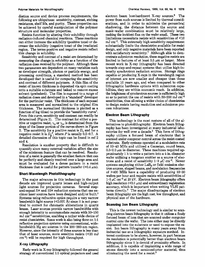
sensitivity to radiation-induced degradation and poor dry-etching pattern-transfer characteristics. The elec- tron beam exposure dose is -100 pC cm-2 at 20 kV,29 while more than 1 J cm-2 is required for deep-UV ~ a t t e r n i n g . ~ l - ~ ~ However, the high-resolution charac- teristics of PMMA have prompted several investigators to examine substituted methacrylates to improve sen- sitivity and etching resistance. The scission efficiency of polymers is typically described in terms of the G value, defined as the number of chemical events per 100 eV of radiation absorbed.34 The higher the Gscission (G,) value, the higher is the susceptibility to radiation-in- duced degradation, and improved resist sensitivity is expected. The efficiency of main-chain cleavage in the case of PMMA can be improved by substitution of the backbone a-methyl group with electronegative groups such as C1 or CN,= by the introduction of bulky groups that provide steric hindrance to weaken the main chain of the polymer,36 or by improving the absorption characteristics of the polymer.% Figure 9 correlates the electron beam sensitivity and G, values for a variety of acrylic polymers. One of the first reports correlating the acrylate substitution pattern with ease of chain scission was the work of Helbert and co-w0rkers.3~ This work predicted that copolymerization of methyl meth- acrylate with a-substituted chloro or cyano acrylates should effectively enhance the polymer's susceptibility to main-chain degradation. Values of G , as high as 6.7 were reported for a-chloroacrylonitrile-methyl meth- acrylate copolymers [P(CAN-MMA)] compared with 1.5 for PMMA. Subsequently, Pittman and co-work- e r ~ ~ * ~ ~ prepared copolymers of methacrylonitrile and methyl a-chloroacrylate that exhibited electron beam sensitivities - 5 times higher than that of PMMA (20 vs 95 gC cm-2 at 15 kV).
Incorporation of fluorine into the ester group of PMMA has been shown to be another method of im- proving the sensitivity of PMMA to radiation-induced degradation. Examples include poly(2,2,3,4,4,4-hexa- fluorobutyl methacrylate) (FBM)40 and poly(2,2,2-tri- fluoroethyl 2 - ~ h l o r o a c r y l a t e ) . ~ ~ ~ ~ ~
Inter- and intramolecular anhydride formation is also an effective means of enhancing the electron beam sensitivity of methacrylates. R ~ b e r t s ~ ~ ? ~ ~ prepared terpolymers of methyl methacrylate, methacrylic acid, and methacryloyl chloride and induced the formation of intermolecular anhydride cross-links by first pre- baking the resist-coated substrate. The anhydride
R
fCH2-C-SO2-f;
R'
PES: R=H,R'=CH2CH3 I I PMPS: R'CH3,R1=CH2CH~CH3
PSS: R = H,R' = C ~ H ~
Figure 10. Structure of the poly(o1efii sulfone) resist materials.
linkages were subsequently cleaved on irradiation, re- storing solubility to the irradiated regions. In a com- parable approach, workers at IBM& developed a "ter- polymer'' resist comprised of methyl methacrylate, methacrylic anhydride, and methacrylic acid. Opti- mization of the monomer ratios afforded sensitivities of 15-20 pC cm-2 at 25 kV. In this instance, sensitivity enhancement stems from the incorporation of radia- tion-sensitive anhydride linkages aided by the excess strain in the polymer chain due to the cyclization. Similar sensitivity enhancement has been observed for methyl methacrylate-itaconic acid and -methyl ita- conate copolymer^.^^*^^
PMMA also is degraded by deepUV irradiation (A, = 220 nm) but its sensitivity is much too low for practical application. In order to enhance sensitivity, researchers have taken the approach of copolymerizing MMA with more absorbing UV-sensitive components. Wilkins et a1.48149 copolymerized MMA with the UV- sensitive 3-oximino-2-oxobutyl methacrylate (OM).60 The a-keto oxime chromophore has a strong absorption maximum at -220 nm that extends to -240-250 nm. The ester possesses a N-O bond that is photbchemically labile yet sufficiently thermally stable so as to be com- patible with microelectronic processing. Irradiation results in cleavage of the N-0 bond, leading to decar- boxylation and main-chain scission. P(MMA-OM) is up to 5 times more sensitive than PMMA to deep-UV exposure (220-280 nm). Further enhancement in sen- sitivity is obtained by incorporating methacryl~nitrile~~ into the polymer backbone. The addition of benzoic acid sensitizer^^^ has been reported to yield further improvement in sensitivity. The mechanism is believed to be one of singlet excitation. Similar observations have been made for PMMA.52
The incorporation of indenone into the PMMA chain enhances the UV absorption of the resist and, in ad- dition, adds strain to the polymer backbone through the five-membered ring.53 The indenone segment readily undergoes a-cleavage, generating a radical on the polymer backbone that subsequently undergoes p- scission.
Another class of "chain scission" positive resists is the poly(o1efin sulfones). These polymers are alternating copolymers of an olefin and sulfur dioxide having the general structure shown in Figure 10. The relatively weak C-S bond is readily cleaved upon irradiation, and several sensitive resists have been developed based on this chemistry." One of these materials, poly( l-butene sulfone) (PBS) has been made commercially available for mask making.55@ PBS exhibits an electron beam sensitivity of 1.6 pC cm-2 at 20 kV and 0.25-pm reso- lution.
Solution Inhibition Resists
This class of resists operates via a dissolution inhi- bition mechanism and is typically composed of two components. The major component in most resists of this type is an alkali-soluble resin that is rendered in-

1280 Chemical Reviews, 1989, Vol. 89, No. 6 wN2 @ ' + N z
R R
Reichmanis and Thompson
WOLFF a: REARRANGEMENT
BASE INSOLUBLE SENSITIZER
0 ' 0
@.OH R Q5 R
BASE SOLUBLE PHOTOPRODUCT
KETENE
Figure 11. Photochemically induced reaction of a typical sub- stituted diazonaphthoquinone dissolution inhibitor.2
soluble in aqueous alkaline solutions through incorpo- ration of a hydrophobic, radiation-sensitive material. Upon irradiation, the hydrophobic moiety may be either removed or converted to an alkali-soluble species, al- lowing selective removal of the irradiated portions of the resist by an alkaline developer.
The best known dissolution inhibition resist is "conventional positive photoresist", a photosensitive material that uses a novolac (phenol-formaldehyde) polymer with a diazonaphthoquinone photoactive dis- solution inhibitor (PAC). The novolac matrix resin is a condensation polymer of a substituted phenol (often cresol) and formaldehyde. These resins are soluble in organic solvents, facilitating spin coating of uniform, high-quality, glassy films. In addition, they are soluble in basic solutions such as aqueous sodium hydroxide (NaOH) or tetramethylammonium hydroxide (TMAH). The novolac is rendered insoluble in aqueous base through the addition of 10-20 w t % of the PAC. Upon irradiation, the diazoquinone undergoes a Wolff rear- rangement followed by hydrolysis to generate a base- soluble indenecarboxylic acid (Figure ll).57 The ex- posed regions of the film may then be removed by treatment with aqueous base.
While the basic components of all conventional photoresists are the same, the precise performance characteristics depend on the substitution pattern on the novolac resin and/or PAC. Hanabata and co- workers have evaluated the relationship between cre- sol-novolac structure and resist contrast, sensitivity, and exposure latitude.58 Understanding those rela- tionships led to the development of a photoresist with improved resolution and sensitivity to 405-nm radiation. The effect of novolac structure on the dissolution ki- netics has been studied by Templeton, Szmanda, and Z a m ~ i n i . ~ ~ From this study a model is proposed that relates the dissolution rate to intermolecular interac- tions and is useful in the design of resist-developer systems. Similarly, Trefonas et al. have evaluated PAC structure with respect to development rates, resist im- age quality, and overall performance.@' Generally, their findings show that multiple diazonaphthoquinone units per PAC molecule lead to improved resist contrast and image quality.
The absorption characteristics of the resist, and thus the sensitivity of the resist to a particular wavelength, are largely determined by the structure of the diazo- naphthoquinone inhibitor. Most photoresists designed for 365-436-nm irradiation utilize a 5-aryl sulfonate diazaoquinone ester that exhibits absorbance maxima
8 0.6 - e 0.5 - w 4 0.4 -
C
0.2 0'31 0 , l t
0.01' ' I " ' ' I . ' I ' 1 ' I ' ' " 1 1 , ' J 250 300 350 400
Wavelength (nm)
Figure 12. Ultraviolet absorption spectrum of a typical positive photoresist before and after exposure.2
at -340,400, and 430 nm. A typical absorption spec- trum of such a resist is shown in Figure 12. Exposure to 350-450-nm radiation leads to bleaching of the ab- sorbance in that region and formation of the corre- sponding indenecarboxylic acid. Changes in the posi- tion of the aryl substituent can lead to variations in sensitivity and light absorption. For example, the Caryl sulfonate analogues exhibit absorption characteristics that are more appropriate for shorter wavelength irra- diation, i.e., 313 and 365 nm.2 This substitution pattern leads to the appearance of a bleachable absorbance at -315 and 385 nm, extending sensitivity to shorter wavelengths. Optimization of resist sensitivity for a particular exposure tool requires an understanding of the effect of substituents on the absorption character- istics of the materials. This approach was used effec- tively by Miller and co-workers,61 who coupled such studies with semiempirical calculations to facilitate the design of diazonaphthoquinone dissolution inhibitors for mid-UV (-313 nm) applications.
One deficiency of novolac resins is their low glass transition temperature ( Tg), which usually ranges from 70 to 120 "C. It would be desirable to have materials exhibiting thermal stability up to 200 OC to maximize image stability during processing. This requirement has prompted investigators to search for other phenolic polymers as replacements for novolacs. The candidates include poly(p-hydroxystyrene),62 poly@-hydroxy-a- methyl~tyrene):~ and N-@-hydroxypheny1)maleimide copolymers.64 To date, none of these alternatives has been commercialized due to either synthetic difficulties or unacceptably high dissolution rates.
While the novolac-diazonaphthoquinone resists are sensitive, high-resolution "conventional" photoresists, the films are essentially opaque to radiation below 300 nm. The high absorbance below 300 nm requires ex- tended exposure to degrade the dissolution inhibitor near the resist-substrate interface and results in poor image quality. Willson and c o - ~ o r k e r s ~ ~ have reported an alternative dissolution inhibitor for novolac resins based on Meldrum's acid (Figure 13). This compound contains a bleachable chromophore that is sensitive at 250 nm. Irradiation leads to a Wolff rearrangement, producing a ketene intermediate that further degrades t o acetone and carbon monoxide. This system showed

Polymer Materials for Microlithography
r 1
Chemical Reviews, 1989, Vol. 89, No. 6 1281
NOVOLAC/PMPS
L
3CO + A Figure 13. Structure and photochemical reaction of the Meld- rum's acid dissolution inhibitor.
L OH R' ' 0 - C - R ' ~ ] - aNo C - R /I t R'C02H
0
Figure 14. Structure and photochemical reaction of a 2-nitro- benzyl carboxylate dissolution inhibitor.
reasonable sensitivity and resolution although the in- herent absorption of the novolac resin led to attenuation of light through the thickness of the polymer film and consequently poor resist profiles. Additionally, the Meldrum's acid derivatives were relatively volatile and evaporated from the resist films during prebake. This problem was overcome through the incorporation of amide (or lactam) functionalities into the inhibitor structure.M The new inhibitors were employed with a variety of matrix resins, including novolacs, acrylates, and imide polymers.
An alternate two-component positive deepUV resist system was developed by workers at AT&T Bell Lab- oratories.67 This material was based on an optically transparent, aqueous alkali soluble methyl meth- acrylatemethacrylic acid copolymer as the matrix resin containing a 2-nitrobenzyl carboxylate (Figure 14) as the dissolution inhibitor. Irradiation induces rear- rangement and subsequent degradation of the ester, yielding a carboxylic acid plus a nitrosobenzaldehyde. Optimum results were obtained for ester derivatives of large-molecule organic acids such as cholic acid. These esters are nonvolatile, are compatible with the acidic matrix resin, and additionally allow conversion of a relatively large volume fraction of resist from an alka- li-insoluble to an alkali-soluble state. These resists exhibit high sensitivity and contrast and are capable of submicron resolution.
Resist systems based on dissolution inhibition have application not only to photoresist technology but also to electron beam lithography as well. Conventional positive photoresists, for example, have been used for electron beam p r o c e s ~ e s ; ~ ~ ~ ~ however, they exhibit poor sensitivity. A novel electron beam sensitive dissolution inhibition resist was designed by Bowden et al. based on the use of a novolac resin with a poly(o1efin sulfone) dissolution inhibitor.70 The aqueous base soluble no- volac is rendered less soluble via addition of - 10 wt % poly(2-methyl-1-pentene sulfone) (PMPS). Irradiation causes main-chain scission of PMPS followed by de- polymerization to volatile monomer^,^^^^^ which diffuse through the matrix to the surface of the resist and are
SOLID SOLUTION I
PMPS (40%) \
NOVOLAC (Il=6-10)
CH3
Figure 15. Structure and radiation-induced reaction of the IWR resist system.
P&B' FLOOD EXPOSE
A DEVELOP
R A
0
@"' 5 R
R
coon w R
Figure 16. Image reversal process and related chemistry based on a conventional positive photoresist and monoazoline.2
removed by the vacuum system. The dissolution in- hibitor is thus effectively "vaporized", thereby restoring solubility in aqueous base to the irradiated portions of the resist (Figure 15). The sensitivity of this resist, known as NPR, is 3-8 pC cm-2 at 20 kV. Its dry-etching characteristics are comparable to those of the novo- lac-based photoresists, and 0.125-pm resolution has been d e m ~ n s t r a t e d . ~ ~ J ~ Resist systems based on this chemistry have also been reported by workers at Hi- tachP5 and IBM.76
Nonconventional Resist Chemistry
Through creative chemistry and resist processing, schemes have been developed that produce negative- tone images in positive photoresist. One embodiment of these "image reversal" processes requires addition of small amounts of base additives such as monazoline, imidazole, or triethanolamine to diazoquinone-novolac r e ~ i s t s . ~ ~ - ~ ~ The doped resist is exposed through a mask, baked after exposure, flood exposed, and finally de- veloped in aqueous base to generate high-quality neg- ative-tone images. The chemistry and processes asso- ciated with this system are shown in Figure 16. Thermally induced, base-catalyzed decarboxylation of the indenecarboxylic acid destroys the aqueous base solubility of the exposed resist. Subsequent flood ex- posure renders the previously masked regions soluble in aqueous base, allowing generation of negative-tone patterns. It is not always necessary to add the base to the resist prior to exposure. Alternate image reversal

1282 Chemical Reviews, 1989, Vol. 89, No. 6 Reichmanis and Thompson
SENSITIZER (SI ACID ( A )
H H I -CH,-!-
-CH2-C-
Q OH
0 t - euoco
II 0
Figure 17. Chemical reactions associated with a typical chem- ically amplified resist system.2
processes have been developed involving treatment of exposed photoresist with a gaseous amine in a vacuum environment.80
As device features move into the submicron regime requiring development of advanced processing tech- niques and introduction of new lithographic technolo- gies, resist materials with improved etching resistance, resolution, and sensitivity will be required. One ap- proach to improving sensitivity involves the concept of chemical amplification.81*82 Aryldiazonium, diaryl- iodonium, and triarylsulfonium metal halides, for ex- ample, dissociate upon irradiation to produce an acid that can, in turn, catalyze a variety of bond-forming or bond-breaking reactions in a surrounding matrix. The quantum efficiency of such reactions is thus effectively much higher than the quantum yield for initial onium salt dissociation.
This principle has been used to design a number of negative resists based on acid-catalyzed cationic po- lymerization of appropriate monomers,81i83-85 However, such materials generally exhibit poor contrast and resolution. A notable exception is a three-component resist developed by Feely et a1.% consisting of a blend of novolac resin, melamine cross-linking agent, and acid generator. Irradiation of the three-component resist generates an acid catalyst that induces formation of a cross-linked network between the novolac matrix resin and amine additive.
Ito et al. have applied chemical amplification to the development of high-resolution positive resist materials. Their initial studies dealt with the catalytic deprotec- tion of poly(tert-butoxycarbonyloxystyrene) (PBOC- S)82787-89 in which the thermally stable, acid-labile, tert-butoxycarbonyl group is used to mask the hydroxy functionality of poly(vinylpheno1). As shown in Figure 17, irradiation of PBOCS films containing small amounts of an onium salt such as diphenyliodonium hexafluoroarsenate with UV light liberates an acid species that upon subsequent baking catalyzes cleavage of the protecting group to generate poly@-hydroxy- styrene). While this reaction will take place at room temperature, it is accelerated at 100 "C, requiring only a few seconds of baking time. In the absence of acidic species, the protected polymer undergoes no degrada- tion during prolonged heating at 100 OC and requires temperatures in excess of 200 "C to thermally initiate the deprotection reaction. Loss of the tert-butoxy- carbonyl group results in a large polarity change in the exposed areas of the film. Whereas the substituted phenol is a nonpolar material, soluble in nonpolar, li- pophilic solvents, poly(vinylpheno1) is soluble in polar organic solvents and aqueous base. This change in polarity allows formation of either positive or negative images, depending upon the polarity of the developer. Nonpolar solvents such as a mixture of dichloromethane
Figure 18. Structure of 2,6-dinitrobenzyl tosylate.
and hexane remove the unirradiated regions, generating a negative image, while an aqueous base developer such as TMAH in water selectively removes the irradiated regions. These resists are sensitive to deep-UV and electron beam irradiation. They may be sensitized to longer wavelengths through the addition of appropriate mid- and near-UV dyes.
Recently, nonionic acid precursors based on nitro- benzyl ester photochemistry have been developed for chemically amplified resist processes.w92 The ester- based systems (Figure 18) exhibit a number of advan- tages over the onium salt systems for lithographic ap- plications. Specifically, the esters are easily synthesized, are soluble in a variety of organic solvents, are nonionic in character, and contain no potential device contam- inants such as arsenic or antimony. In addition, their absorption characteristics are well suited for deep-UV exposure.
Positive working, self-developing resists based on the photogeneration of acidic species from onium salt sen- sitizers have also recently been rep0rted.9~ One example relies on the acid-catalyzed cleavage of main-chain acetal linkages in poly(phthala1dehyde). Cleavage of just one linkage can lead to rapid depolymerization effecting self-development. Addition of either tri- phenylsulfonium or diphenyliodonium hexafluoro- arsenate allowed imaging of 1-pm-thick films of poly- (phthalaldehyde) at exposure doses of 2-5 mJ cm-2 and 1.0 p C cm-2 for deep-UV and electron beam irradiation, respectively. Submicron patterns were obtained im- mediately following postexposure baking without any subsequent "development" step. Similarly, linear ter- tiary polycarbonates have been investigated for their utility as self-developing UV and electron beam re- sists.- These condensation polymers readily undergo acid-catalyzed thermolysis to generate carbon dioxide, alkenes, and alcohols as volatile products.
The polyphthalaldehydes and polycarbonates are among a growing number of resist systems that require no development step. Such dry development may im- prove resolution in both positive and negative resists since image distortion due to resist swelling in solution development is no longer a factor. However, their re- sistance to subsequent lithographic processing steps is generally found to be poor. An alternative approach described by Taylor et al.97-99 has been to effect a dif- ferential plasma-etching rate in the resist upon irra- diation. This approach is most effectively accomplished via a two-component resist system involving incorpo- ration of a monomer guest into a host polymer. Irra- diation effects polymerization of the guest monomer and some degree of grafting to the host. A vacuum bake removes the monomer from the unexposed regions, producing a negative-tone relief image. Appropriate selection of the guest monomer allows subsequent plasma development to afford either positive or negative images. Guest monomers may either by vinyl-substi- tuted aromatics such as N-vinylcarbazoleg8 or organo- metallic species such as bis(acryloxybuty1)tetra- methyldisiloxaneW that produce nonvolatile metal ox-

Polymer Materials for Microlithography Chemical Reviews, 1989, Vol. 89. No. 6 1283
ization is important to produce a perfectly level surface that will minimize depth-of-focus problems associated with variations in film thickness resulting from topo- graphic features on the wafer surface, induced from previous processes. Important characteristics for a planarizing polymer system include dry-etching re- sistance, solution viscosity, flow characteristics at both room and elevated temperature, thermal stability, and ease of final stripping.
Stillwagon et alJM recently presented a mathematical model that allows the calculation of the important flow and thermal material properties required for planari- zation. Two approaches have been used to provide g d local and global planarization. First, planarizing layers consisting of relatively low Tg materials that can be spin coated from solution and flowed in a low-viscosity state prior to curing have achieved 70-90% planarization over an entire wafer. Alternatively, planarizing layers of a low-viscosity epoxy resin containing an onium salt curing agent that is spin coated without solvent, allowed to stabilize, and then cured to a high Tg film have shown excellent planarization properties. A good review of the planarization process and materials has been recently published, and the reader is referred to this review for more detailed information.'03
A novel multilevel technique, known as contrast en- hancement (CEL), addresses the problem associated with a reduction in the contrast of the aerial image that occurs as the resolution limit of an optical imaging system is approached.'0P-106 As line width decreases, the contrast between the projected clear and opaque regions of a mask deteriorates as does the ability of the resist to resolve those features. The CEL technique improves contrast of the aerial image in the resist, thereby leading to a sharper latent image and improved resolution. The process utilizes photobleachahle materials that are opaque before exposure but bleach (i.e., become transparent) on exposure to radiation. The materials are coated directly onto the surface of the resist. The dynamics of the bleaching process are such that the transmitted image is of much higher contrast than the incident aerial image,'05 thereby improving the resist's ability to discriminate mask features. The optical density of CEL films should be greater than 2 for thicknesses less than 0.5 pm.
The first CEL system described by Griffing and West'" consisted of an organic dye dispersed in an inert polymer fii. The material is spin cast onto the surface of the resist and subsequently removed following ex- posure but prior to resist development. The chemistry of this system is based on the photoisomerizatiou of an aromatic dye to an o~aziridine.~~'J~* Several applica- tions have been presented that demonstrate the ad- vantages of this two-level CEL process over conven- tional single-level l i th~graphy. '~~
A single-component CEL system based on the pho- tobleaching of polysilanes was reported hy Hofer et al."' This mid-UV material takes advantage of the shift in the absorption maximum of polysilanes to shorter wavelengths upon radiation-induced chain scission. The first water-soluble CEL was reported by Halle."' Photofragmentation of an aryldiazonium sulfate in the presence of atmospheric moisture affords an aqueous- soluble phenol that facilitates removal of the CEL during resist development. Diazonium salts have also
..... . . . . ... . . . .., PUWIRIZIWG U I E R TOPOGRAPHIC F E B U R E
BUWiiEl EXPOSURE
OEYELOQlEYl OEYELOQIEWT
W E V E l C H CAQPEO UWCAPPEO RIE Q C l EXPOSURE I C Y EXQOSURE QCM QCM
Figure 19. F" aequence for several multilevel mist schemes!
ides upon oxygen plasma treatment. Sensitive X-ray resists requiring exposure doses on the order of 1-2 mJ cm-' have been developed on the basis of the above chemistry.
Multilevel Resist Chemistry
The increasing complexity and miniaturization of integrated circuit technology are pushmg conventional single-layer resist processes to their limit. The demand for improved resolution requires imaging features with increasingly higher aspect ratios and smaller line-width variation over steep substrate topography. The de- crease in feature size can lead to other problems asso- ciated with the particular lithographic technique em- ployed. For instance, in photolithography, feature size can be affected by standing-wave effects and reflections from the substrate surface, which limit the resolution attained with optical techniques. A number of schemes have been proposed to address these problems, in- cluding the use of polymeric planarizing layers, anti- reflection coatings, and contrast enhancement materi- als." These techniques can be conveniently divided into two broad catagories. The first includes those systems employing a separate planarizing layer that may be developed with wet or dry (RIE) techniques. The second catagory uses thin organic films that have precisely designed light absorption characteristics. Antireflective coatings are designed to be highly ab- sorbing at the exposure wavelength and are applied beteen the substrate and the resist. Contrast en- hancement materials are generally applied to the sur- face of the resist and through photochemical bleaching during exposure, improve the quality of the aerial light image.
The available planerization processes are summarized in Figure 19. Most of these approaches are based on spin coating thick (1-2 pm) films of thermoplastic materials such as PMMA, polystyrene, polyimide, or novolac resins (usually in conventional photoresist formulations) onto the surface of the wafer. There are two types of planarization that are important for li- thography'O' (1) local planarization, which is the ability to planarize closely spaced features, and (2) global planariation, which is the extent to which a large area (wafer) with both closely spaced and isolated features is planarized.
Local planarization is easily achieved by spin coating a polymer and baking; however, global planarization is almost never achieved by this process. Global planar-

1284 Chemical Reviews, 1989, Vol. 89, No. 6 Reichmanis and Thompson
While trilevel lithography is a time-consuming pro- cess requiring precise control of several processing steps, it improves the resolution capability of conventional resists by separating the imaging fluction of the resist from the subsequent etch mask function and permits imaging in a relatively thin resist film.
A simplification of trilevel lithography involves com- bining the properties of the top imaging layer with those of the oxygen RIE resistant intermediate layer into a single layer that is coated onto the surface of the thick planarizing layer. Conventional processing allows pattern definition of this upper layer, and the pattern is then transferred to the substrate by oxygen RIE techniques.
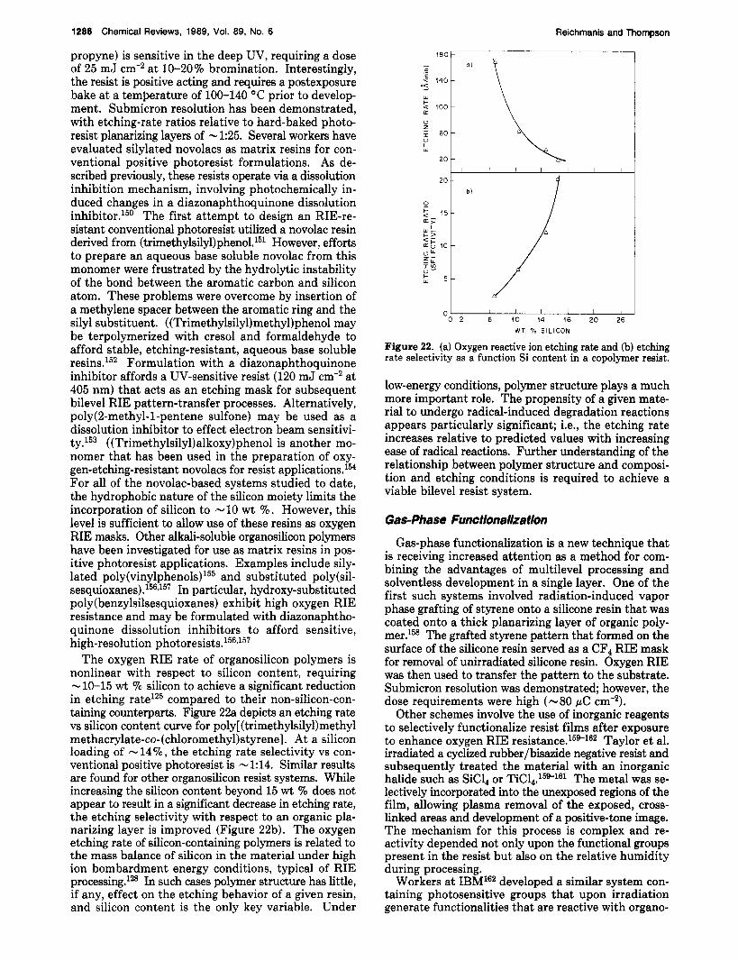
Organosilicon polymers are ideal candidates for bi- level lithography.lB Treatment of organometallic com- pounds, particularly organosilicon materials, with an oxygen plasma leads to the formation of the corre- sponding metal oxide. Taylor and Wolf have shown that incorporation of silicon into organic polymers renders them resistant to erosion in oxygen plasmas.lZ6 This surface passivation results from the formation of a protective coating of Si02 on the polymer surface. Modeling studies predict that the thickness of this layer should be about 50 A, a value that has been confirmed by surface a n a l y s i ~ . ~ ~ ~ J ~ ~ The preliminary work of Taylor et al. has led to development of numerous sili- con-containing resist systems for bilevel lithography utilizing RIE pattern transfer. However, there are several problems with silicon-containing polymers that may interfere with their lithographic performance. A decrease in glass transition temperature (T ) often ac- companies the incorporation of silicon into tke polymer chain and may cause dimensional instability of patterns during processing. In addition, most useful silicon substituents are hydrophobic in nature, which poten- tially could cause problems for those resist systems that use aqueous-base developers.
The first organosilicon polymers examined for use in bilevel RIE processes were the polysiloxanes.129J30 These resists were based on copolymers of dimethyl- siloxane, methylphenylsiloxane, or methylvinylsiloxane. They are negative photoresists and electron beam re- sists that exhibit oxygen RIE erosion rates of 1-3 nm min-' compared to -80 nm min-' for hard-baked pos- itive photoresist. While high resolution has been achieved with these materials, the imaging layer must be kept thin to avoid problems associated with creep of the developed pattern arising from the low Tg of the siloxanes (<30 "C). The initial reports of the utility of polysiloxanes for lithographic application spurred sev- eral research groups to further investigate this class of materials. Workers at Nippon Telephone and Tele- graph have addressed the problem of low Tg by pre- paring chloromethylated poly(diphenylsiloxane).131J3z More recently, poly(silsesquioxanes)133J34 have been reported as sensitive, negative, electron beam, ion beam, and UV resists. These soluble "ladder-type" polymers, prepared by the hydrolysis of substituted chloro- and alkoxysilanes, are high-T, materials (150 "C) with high silicon contents. Block copolymer chemistry provides a convenient means of incorporating the oxygen RIE resistant polysiloxane moiety into a high-Tg: radia- tion-sensitive p01ymer.l~~ The flow characteristics of such resists are determined by the higher Tg moiety,
been used as CEL materials1" by workers at Hitachi. It is predicted that CEL techniques will extend res-
olution to feature sizes as small as 0.4X/NA, or -0.6 pm for currently available exposure tools operating at 405 and 436 nm113 [NA is the numerical aperture of the exposure system (see ref 2 for more details)]. The currently available materials afford improved resolu- tion, improved yield, and increased process 1 a t i t ~ d e . l ~ ~ Further developments to achieve practical water-soluble systems plus a better match with the absorption char- acteristics of the resist would be desirable.
Multilevel Resist Processes Employing Reactive Ion Etching Pattern-Transfer Techniques
The contrast enhancement and antireflective coating materials discussed in the previous section both are used in conjunction with the standard wet-developed photoresist process. Multilevel resist processes that utilize a thick planarizing layer differ from the above processes in both purpose and process complexity. The purpose of these techniques is to separate the imaging layer from the process etch mask, and they provide improved imaging characteristics for the overall litho- graphic process. There are two generic types of pro- cesses used, viz., liquid developed and dry developed. The liquid-developed processes have been extensively discussed by Lin in ref 100 and will not be covered in this review. The dry-developed processes that use re- active ion etching (RIE) for pattern transfer into the planarizing layer have received considerable attention and use materials with properties that depend on the specific strategy employed. There are two schemes that have been used-trilevel and bilevel-and these are discussed below.
Trilevel processing begins with the planarization of device topography with a thick layer of some organic polymer such as a polyimide or positive photoresist that has been "hard-baked" (baked to induce cross-linking), or otherwise treated, to render it insoluble in most solvents. Next, an intermediate RIE barrier such as silicon dioxide is deposited, and finally the structure is coated with the desired resist material. A pattern is delineated in the top resist (imaging) layer and subse- quently transferred into the planarizing layer by dry- etching te~hniques . l '~J~~
Several variations of this generic process have been reported. The most common intermediate oxygen RIE barrier layer is SiOz. Thin films of SiOz may be de- posited by sputtering, plasma CVD,llG or spin coating SiOz organic precursor^.^^^-^^^ The organic precursors are often referred to as spin-on-glasses (SOG). While SOG layers greatly simplify trilevel processing through the elimination of costly vapor phase deposition steps, they are likely to contain a higher number of defects than vapor-deposited films."g Proper storage and dispensing techniques can minimize these problems but they increase the complexity of processing. Alternative intermediate layers include silicon nitride,ll5JZ0 sili- con,121 germanium,122 and arsenic sulfide.lZ3 Antire- flection properties can be incorporated either through the use of an inherently highly absorbing polymer as the planarizing layer or by the addition of a dye into the planarizing layer.la Alternatively the absorber can be incorporated into the intermediate RIE barrier lay-

Polymer Materials for Microlithography Chemical Reviews, 1989, Vol. 89, No. 6 1285
polymer molecular weight, enhanced solubility, and positive resist behavior.
An alternative to designing polymers with silicon in the backbone is to incorporate the silicon-bearing functional group into the side chain of existing poly- meric resist systems. Negative resists based on (tri- methylsily1)styrene copolymers with chloro- and (chlo- romethyl)styrene, for example, have been reported by both MacDonald and co-w~rkers '~~ and Suzuki et The silylated styrene imparts oxygen RIE resistance while the chloro- and (chloromethy1)styrene units un- dergo cross-linking reactions giving rise to negative resist behavior. These random copolymers exhibit 0.5-pm resolution and sufficient etching resistance to allow pattern transfer through a thick underlying layer of "hard-baked" positive photoresist. Copolymers of (trimethylsily1)methyl methacrylate with (chloro- methy1)styrene also function as sensitive RIE-resistant negative resists144 even though methacrylates, by themselves, are positive-acting materials. Co- polymerization of the silylated methacrylate monomer with 9 wt % (chloromethy1)styrene results in a resist that is sensitive to both deep-UV and electron beam irradiation with sensitivities of 18 mJ cm-2 and 1.95 p C cm-2, respectively, and capable of submicron resolution. High sensitivity is achieved in these systems through the (chloromethy1)styrene unit, which is highly sus- ceptible to cross-linking. The dose required to cross- link polymers containing even small amounts of (chlo- romethy1)styrene is well below that required to cause substantial chain scission in most substituted meth- acrylates. Etching-rate ratios relative to hard-baked positive photoresist of <1:10 under typical oxygen RIE conditions were obtained for these systems. Silylated methacrylates themselves function as positive, bilevel, deep-UV r e ~ i s t s , ~ ~ ~ , ' ~ ~ although the silyl substituent must be carefully selected to avoid an excessive decrease in Tg. For example, poly(pentamethyldisiloxypropy1 methacrylate) is of limited utility in resist applications due to a decrease in Tg.145 (Trimethylsily1)methyl methacrylate polymers are glassy, high-T, materials that can be readily copolymerized with appropriate monomers to effect radiation sensitivity. Poly[ (tri- methylsily1)methyl methacrylate-co-3-oximino-2-oxo- butyl methacrylate] ,l& for example, is a high-resolution, RIE-resistant, deep-UV resist capable of submicron resolution with a sensitivity of - 250 mJ cm-2. Etch- ing-rate ratios with respect to typical planarizing layers are l:(lO-12) for materials containing -10 wt ?% Si. The radiation chemistry of this material involves pho- tolytic cleavage of the N-0 bond, followed by decar- boxylation and main-chain scission. Incorporation of silicon into the side chain of olefin sulfone poly- m e r ~ ~ ~ ~ ~ ~ ~ has been shown to greatly enhance the RIE resistance of these copolymers. Poly(3-butenyltri- methylsilylsulfone) forms a thin protective layer of SiO, during oxygen RIE, allowing pattern transfer through a thick underlying layer of planarizing polymer. This resist exhibits a sensitivity of 2 pC cm-2 at 20 kV and has been used to define 0.05-pm-period gratings in semiconductor substrates. It is among the highest sensitivity, RIE-resistant, positive electron resists known. Another class of silicon-containing polymers was recently reported based on substituted poly- a~ety1enes. l~~ Brominated poly( 1-(trimethylsily1)-
CH3 I
C H 3 CHZCl
' I N D I C A T E S P A R T I A L CHLORINATION
Figure 20. Synthesis of a typical block copolymer useful as a high-resolution resist.
?H3 CH3 ?H3 CH3 t H 3 7H3 CH3 CH3 I I I
I I I I I I I I R R R R R R R R
- S I - $ 1 - S I - S I - &---SI - S I . .SI - SI-
I 1 XH y 3 y 3
1 y 3 y 3 y 3
2 S I + -SI * . S I - H SI - SI- I I 1 I 1 R R R R R
1 FURTHER POLYMER DEGRADATION
R - CH39CeH5 1 CgH44, C ~ ~ H Z J
Figure 21. Structure and radiation-induced reaction of a sub- stituted polysilane.
while problems associated with phase separation are minimized because of the block architecture. Block copolymers of dimethylsiloxane and chlorinated p - methylstyrene have been reported to exhibit good sen- sitivity, good resolution, good thermal properties, and low O2 RIE rates. The synthesis of these materials is outlined in Figure 20. Transmission electron micros- copy shows that the morphology of nearly equimolar compositions of the siloxane-(chloromethy1)styrene block copolymers corresponds to a lamella-like structure with spacing between the lamellae on the order of 50-300 A. Microphase separation is confined to do- mains composed of similar segments and occurs on a scale comparable to the radius of gyration of the poly- mer chain. Auger electron spectroscopy indicates that the surface of these films is rich in silicon followed by a styrene-rich layer. This phenomenon arises from the difference in surface energy of the two phases. The siloxane moiety exhibits a lower surface energy and thus forms the silicon-rich surface layer.
The incorporation of Si-Si, as opposed to Si-0-Si, bonds into the polymer backbone provides resists that undergo chain scission upon exposure to UV radiation. Main-chain scission results in a decrease in polymer molecular weight, and proper selection of a developer allows removal of the more soluble irradiated regions. The polysilanes (Figure 21) are thus positive-acting resists.1m140 They are generally characterized by a high Tg and exhibit oxygen RIE rates similar to those of the polysiloxanes, making them excellent masks for RIE pattern-transfer processes. Several polysilanes self- develop upon exposure to high doses of deep-UV ra- diation and thus require no solvent development. In related chemistry, a condensation polymer p-bis- ((chloromethy1)silyl)benzene has been reported by workers at Hitachi141 to undergo radiation-induced cleavage of the Si-Si linkages, leading to a reduction in
1286 Chemical Reviews, 1989, Vol. 89, No. 6 Reichmanis and Thompson
propyne) is sensitive in the deep UV, requiring a dose of 25 mJ cm-2 at 10-20% bromination. Interestingly, the resist is positive acting and requires a postexposure bake at a temperature of 100-140 "C prior to develop- ment. Submicron resolution has been demonstrated, with etching-rate ratios relative to hard-baked photo- resist planarizing layers of - 1:25. Several workers have evaluated silylated novolacs as matrix resins for con- ventional positive photoresist formulations. As de- scribed previously, these resists operate via a dissolution inhibition mechanism, involving photochemically in- duced changes in a diazonaphthoquinone dissolution inhibitor.lm The first attempt to design an RIE-re- sistant conventional photoresist utilized a novolac resin derived from (trimethy1~ilyl)phenol.'~~ However, efforts to prepare an aqueous base soluble novolac from this monomer were frustrated by the hydrolytic instability of the bond between the aromatic carbon and silicon atom. These problems were overcome by insertion of a methylene spacer between the aromatic ring and the si1 yl subs ti tuen t. ( (Tr ime th ylsil yl) me t hyl) phenol may be terpolymerized with cresol and formaldehyde to afford stable, etching-resistant, aqueous base soluble resins.152 Formulation with a diazonaphthoquinone inhibitor affords a UV-sensitive resist (120 mJ cm-2 at 405 nm) that acts as an etching mask for subsequent bilevel RIE pattern-transfer processes. Alternatively, poly(2-methyl-1-pentene sulfone) may be used as a dissolution inhibitor to effect electron beam sensitivi- ty.153 ((Trimethylsily1)alkoxy)phenol is another mo- nomer that has been used in the preparation of oxy- gen-etching-resistant novolacs for resist app1ications.l" For all of the novolac-based systems studied to date, the hydrophobic nature of the silicon moiety limits the incorporation of silicon to -10 wt %. However, this level is sufficient to allow use of these resins as oxygen RIE masks. Other alkali-soluble organosilicon polymers have been investigated for use as matrix resins in pos- itive photoresist applications. Examples include sily- lated poly(vinylphenols)155 and substituted poly(si1- s e s q u i o ~ a n e s ) . ~ ~ J ~ ~ In particular, hydroxy-substituted poly(benzylsi1sesquioxanes) exhibit high oxygen RIE resistance and may be formulated with diazonaphtho- quinone dissolution inhibitors to afford sensitive, high-resolution p h o t o r e ~ i s t s . ~ ~ ~ J ~ ~
The oxygen RIE rate of organosilicon polymers is nonlinear with respect to silicon content, requiring - 10-15 wt % silicon to achieve a significant reduction in etching ratelz5 compared to their non-silicon-con- taining counterparts. Figure 22a depicts an etching rate vs silicon content curve for poly[ (trimethylsily1)methyl methacrylate-co- (chloromethyl)styrene] . At a silicon loading of - 1470, the etching rate selectivity vs con- ventional positive photoresist is - 1:14. Similar results are found for other organosilicon resist systems. While increasing the silicon content beyond 15 wt % does not appear to result in a significant decrease in etching rate, the etching selectivity with respect to an organic pla- narizing layer is improved (Figure 22b). The oxygen etching rate of silicon-containing polymers is related to the mass balance of silicon in the material under high ion bombardment energy conditions, typical of RIE processing.l% In such cases polymer structure has little, if any, effect on the etching behavior of a given resin, and silicon content is the only key variable. Under
180 1
5 140
4' : I 100
c W
b l
" 0 2 6 40 44 46 20 26 WT. % SILICON
Figure 22. (a) Oxygen reactive ion etching rate and (b) etching rate selectivity as a function Si content in a copolymer resist.
low-energy conditions, polymer structure plays a much more important role. The propensity of a given mate- rial to undergo radical-induced degradation reactions appears particularly significant; i.e., the etching rate increases relative to predicted values with increasing ease of radical reactions. Further understanding of the relationship between polymer structure and composi- tion and etching conditions is required to achieve a viable bilevel resist system.
Gas-Phase Functionalization
Gas-phase functionalization is a new technique that is receiving increased attention as a method for com- bining the advantages of multilevel processing and solventless development in a single layer. One of the first such systems involved radiation-induced vapor phase grafting of styrene onto a silicone resin that was coated onto a thick planarizing layer of organic poly- mer.15* The grafted styrene pattern that formed on the surface of the silicone resin served as a CF4 RIE mask for removal of unirradiated silicone resin. Oxygen RIE was then used to transfer the pattern to the substrate. Submicron resolution was demonstrated; however, the dose requirements were high (-80 FC cm-2).
Other schemes involve the use of inorganic reagents to selectively functionalize resist films after exposure to enhance oxygen RIE resistan~e.'~"'~~ Taylor et al. irradiated a cyclized rubber/bisazide negative resist and subsequently treated the material with an inorganic halide such as SiC14 or TiC14.154-161 The metal was se- lectively incorporated into the unexposed regions of the film, allowing plasma removal of the exposed, cross- linked areas and development of a positive-tone image. The mechanism for this process is complex and re- activity depended not only upon the functional groups present in the resist but also on the relative humidity during processing.
Workers at IBM162 developed a similar system con- taining photosensitive groups that upon irradiation generate functionalities that are reactive with organo-

Polymer Materials for Microlithography
metallic reagents. The most promising candidates are nonpolar lipophilic resists such as PBOCS discussed earlier. This material is converted to poly(vinylpheno1) after irradiation and postexposure bake via acid-cata- lyzed cleavage of the tert-butoxycarbonyl group. The poly(vinylpheno1) thus generated is reactive toward silylating agents so that treatment with an organosilicon reagent such as hexamethyldisilazane (HMDS) or chlorotrimethylsilane results in selective incorporation of silicon into the irradiated parts of the film, allowing high-resolution oxygen RIE pattern transfer. Alterna- tively, the photochemically generated poly(hydroxy- styrene) regions of the film may be treated with a re- active dye to generate a mask for subsequent deep-UV exposure and development of the previously masked portions of the film.163 Another approach utilizes con- ventional novolac-diazoquinone chemistry to induce differential reactivity toward an organometallic reagent. Submicron resolution has been demonstrated for 365- 405-nm radiati011.l~~
Chemical Reviews, 1989, Vol. 89, No. 6 1287
(4) Moreau, W. M. Semiconductor Lithography: Principles, Practices, and Materials; Plenum: New York, 1988.
(5) Pol, V.; Bennewitz, J. H.; Escher, G. C.; Feldman, M.; Firtion, V. A.; Jewell, T. E.; Wilcomb, B. E.; Clemens, J. T. Proc. SPIE, Optical Microlithography V 1986,633,6.
(6) Spears, D. L.; Smith, H. I. Solid State Technol. 1972,15,21. (7) Taylor, G. N.; Wolf, T. M. J. Electrochem. SOC. 1980, 127,
2665. (8) Alles, D. S.; Biddick, C. J.; Bruning, J. H.; Clemens, J. T.;
Collier, R. J.; Gere, E. A.; Harriott, L. R.; Leone, F.; Liu, R.; Mulrooney, T. J.; Nielsen, R. J.; Paras, N.; Richman, R. M.; Rose, C. M.; Rosenfeld, D. P.; Smith, D. E. A.; Thomson, M. G. R. J . Vac. Sci. Technol. B 1987,5(1), 47.
(9) Heard, P.; Cleaver, J.; Ahmed, H. J. Vac. Sci. Technol. A 1985. 3. 87.
Conciusion
The constant progress in design and integration of VLSI devices continues to demand increasingly smaller and more precise device features. At the present time, almost all commercial devices are made by photoli- thography utilizing UV radiation in the wavelength range of 365-436 nm. However, within the next 5-8 years, new lithographic strategies will be required to meet resolution needs that will likely extend below 0.5 pm. Technologies under development include electron beam, ion beam, X-ray, and short-wavelength litho- graphies. Electron beam lithography is already an im- portant technology in the manufacture of chromium masks and custom VLSI devices. Each of these alter- native technologies will require new polymeric resist materials and processes. This review article has dis- cussed numerous approaches to resist design applicable to the different lithographic strategies both for single and multilevel processes in which metal-containing polymers find important application.
The future of microlithography is bright and contains many challenges in the areas of resist research and associated processing. By the end of this century, it is almost certain that photolithography at conventional wavelengths will have given way to one of the newer microlithography technologies. Given that assumption, it is highly probable that one or more of the novel chemistries discussed in this article will be used to produce this generation of VLSI devices. A significant base of fundamental understanding has been estab- lished. Without doubt, this understanding will be further refined over the coming years to yield resist materials that meet the demands of the emerging technologies.
References (1) Thompson, L. F.; Kerwin, R. E. Annu. Reu. Mater. Sci.
(Huggins, R. A., Bube, R. H., Roberts, R. W., Eds.) 1976,6,
(2) Thompson, L. F. In Introduction to Microlithography; ACS Sym osium Series 219; Thompson, L. F., Willson, C. G., Bowxen, M. J., Eds.; American Chemical Society: Washing- ton, DC, 1983.
(3) Bowden, .M. J.; Turner, S. R., Eds. Electronic and Photonic Applicatzons of Pol mers; ACS Advances in Chemistry Se- ries 218; American demical Society: Washington, DC, 1988.
267-301.
(10) Novembre, A. E.; Masakowski, L. M.; Hartney, M. A. Polym. Eng. Sci. 1986, 26(16), 1158.
(11) Thommon, L. F.: Doerries, E. M. J. Electrochem. SOC. 1979. . . 126(16), 1699-702.
(12) Minsk, L. M. US. Patent 2725372, 1955. (13) Iwayanagi, T.; Kohashi, T.; Nonogaki, S.; Matsuzawa, T.;
Douta, K.; Yanazawa, H. IEEE Trans. Electron Devices
(14) Hashimoto, M.; Iwayanagi, T.; Shiraishi, H.; Nonagaki, S. Proceedings of the Regional Technical Conference on Pho- topolymers, Mid-Hudson Section, SPE, Ellenville, NY, 1985, p 11.
(15) Hartney, M. A.; Tarascon, R. G.; Novembre, A. E. J. Vac. Sci. Technol. E 1985, 3, 360.
(16) Choong, H. S.; Kahn, F. J. J . Vac. Sci. Technol. 1981,19(4), 1121.
(17) Tan, 2. C.; Petropoulos, C. C.; Rauner, F. J. J. Vac. Sci. Technol. 1981, 19(4), 1348.
(18) Bartelt, J. L. Appl. Polym. Symp. 1974, 23, 139. (19) Hirai, T.; Hatano, Y.; Nonogaki, S. J. Electrochem. SOC. 1971,
1981, ED-28(11), 1306-10.
118(4), 669. (20) Thompson, L. F.; Feit, E. D.; Heidenreich, R. D. Polym. Eng.
Sci. 1974, 14(7), 529-33. (21) Feit. E. D.: ThomDson. L. F.: Heidenreich. R. D. ACS Diu. . .
Org.’ Coat. ’Plast. h e m . , Prepr. 1973, 383.’ (22) Taniguchi, Y.; Hatano, Y.; Shiraishi, H.; Horigome, S.; No-
nogaki, s.; Naraoka, K. Jpn. J . Appl. Phys. 1979,28, 1143. (23) Taylor, G. N.; Wolf, T. M. J. Electrochem. SOC. 1980, 127,
2665. (24) Tabata, Y.; Tagawa, S.; Washio, M. In Materials for Mi-
crolithography; ACS Symposium Series 266; Thompson, L. F., Willson, C. G., Frechet, J. M. J., Eds.; American Chemical Society: Washington, DC, 1984; pp 151-63.
(25) Thompson, L. F.; Doerries, E. M. J. Electrochem. SOC. 1979, 126(10). 1699-702. .~ ,, ~
(26) Thompson, L. F.; Yau, L.; Doerries, E. M. J. Electrochem.
(27) Feit, E. D.; Thompson, L. F.; Wilkins, C. W., Jr.; Wurtz, M. E.: Doerries. E. M.: Stillwagon. L. E. J . Vac. Sci. Technol.
SOC. 1979, 126(10), 1703-8.
1979, 16(6),’1997. ’ (28) Imamura, S. J. Electrochem. SOC. 1979, 126(9), 1268. (29) Hatzakis, M. J . Electrochem. SOC. 1969, 116, 1033. (30) Ranby, B.; Rabek, J. F. Photodegradation, Photooxidation
and Photostabilization of Polymers, Wiley: New York, 1975; DD 156-9.
(31) Mimura, Y.; Ohkubo, T.; Takanichi, T.; Sekikawa, K. Jpn. Appl. Phys. 1978, 17, 541.
(32) Lin, B. J. J . Vac. Sci. Technol. 1975,12,1317-20. (33) Chandross. E. A.: Reichmanis. E.: Wilkins. C. W.. Jr.: Hart- . . . ,
less, R. L. Can. 3. Chem. 1983, 61(5), 817l23. (34) Moreau, W. M. Semiconductor Lithography: Principles,
Practices, and Materials; Plenum: New York, 1988; p 96. (35) Helbert, J. N.; Chen, C. Y.; Pittman, C. U., Jr.; Hagnauer, G.
L. Macromolecules 1978, 11, 1104. (36) Moreau, W. M. Proc. SPIE, Submicron Lithogr. 1982,333,
2.
(44)
Helbert, J. N.; Wagner, B. E.; Caplan, J. P.; Poindexter, E. H. J . Appl. Polym. Sci. 1975, 19, 1201-3. Lai, J. H.; Helbert, J. N.; Cook, C. F., Jr.: Pittman, C. U.. Jr. J. Vac. Sci. Technol. 1979, 16(6), 1992-5. Chen, C.-Y.; Pittman, C. U., Jr.; Helbert, J. N. J. Polym. Sci., Polym. Chem. Ed. 1980,18, 169-78. Kakuchi, M.; Sugawara, S.; Murase, K.; Matsuyama, K. J . Electrochem. SOC. 1977,124, 1648. Tada, T. J. Electrochem. SOC. 1979, 126, 1829. Tada, T. J. Electrochem. SOC. 1983,130, 912. Roberts, E. D. ACS Diu. Ora. Coat. Plast. Chem., Prem. . - 1973, 33(1), 359. Roberts, E. D. ACS Diu. Ow. Coat. Plast. Chem.. PreDr. - . - 1977, 37(2), 36.
(45) Moreau, W.; Merritt, D.; Moyer, W.; Hatzakis, M.; Johnson, D.; Pederson, L. J . VUC. Sci. Technol. 1979, 16(6), 1989-91.
(46) Namastse, Y. M. N.; Obendorf, S. K.; Anderson, C. C.; Kra- sicky, P. D.; Rodriguez, F.; Tiberio, R. J. Vac. Sci. Technol. E 1983, 1(4), 1160-5.
1288 Chemical Reviews, 1989, Vol. 89, No. 6 Reichmanis and Thompson
(47)
(57)
Namastse, Y. M. N.; Obendorf, S. K.; Anderson, C. C.; Ro- driguez, F. Proc. SPIE, Adu. Resist Technol. 1984, 469,
Wilkins, C. W., Jr.; Reichmanis, E.; Chandross, E. A. J . Electrochem. SOC. 1980, 127(11), 2510-3. Reichmanis, E.; Wilkins, C. W., Jr.; Chandross, E. A. J . Electrochem. SOC. 1980, 127(11), 2514-7. Delzenne, G. A.; Laridon, U.; Peeters, H. Eur. Polym. J. 1970, 6, 933. Reichmanis, E.; Wilkins, C. W., Jr. Polymer Materials for Electronic Applications; ACS Symposium Series 184; Feit, E. D., Wilkins, C. W., Jr., Eds.; American Chemical Society: Washin on, DC, 1982.
A.; Nakane, H.; Tsumori, T.; Nakane, Y. ACS Diu. Org. Coat. Plast. Chem., Prepr. 1979, 426-31. Hartless, R. L.; Chandross, E. A. J . Vac. Sci. Technol. 1981, 19, 1333-7. Bowden, M. J.; Thompson, L. F. Solid State Technol. 1979, 22. 72.
144-50.
Tsuda, !$ .; Oikawa, S.; Nakamura, Y.; Nagata, H.; Yokota,
Ballantyne, J. P.; Bowde ,
L. F.: Yan. L. D. Microcircuit Engineering: Ahmed. H.:
Pacanskv, J;: Lverla, J. R. IEM 42-55.
(58) Hanabata, M.; Furuta, A.; Uemura, Y. Proc. SPIE, Adu. Re- sist Technol. 1986, 631, 76-82.
(59) Templeton, M. K.; Szmanda, C. R.; Zampini, A. Proc. SPIE, Adu. Resist Technol. 1987, 771, 136-47.
(60) Trefonas. P.. 111: Daniels. B. K.: Fischer. R. L. Solid State TechnoL'l987, 30, 131. '
(61) Miller, R. D.; Willson, C. G.; McKean, D. R.; Tompkins, T.; Clecak, N.; Michl, J.; Downing, J. Proceedings of the Re- gional Technical Conference on Photopolymers: Principles, Processes, and Materials, Mid-Hudson Section, SPE, Ellen- ville, NY, Nov 8-10, 1982, p 111.
(62) Cernigliaro, G. J.; Shipley, C. R. US. Patent 4 439 516, Mar 27, 1984.
(63) Ito, H.; Willson, C. G.; Frechet, J. M. J.; Farrall, M. J.; Ei- chler, E. Macromolecules 1983,16, 510.
(64) Turner, S. R.; Arcus, R. A.; Houle,. C. G.; Schleigh, W. R. Proceedings of the Regional Technical Conference on Pho- topolymers: Principles, Processes, and Materials, Mid- Hudson Section, SPE, Ellenville, NY, Oct 28-30, 1985, pp 35-47.
(65) Grant, B. D.; Clecak, N. J.; Twieg, R. J.; Willson, C. G. IEEE Trans. Electron Devices 1981, ED-28(11), 1300.
(66) Willson, C. G.; Miller, R. D.; McKean, D. R. Proc. SPIE, Ado. Resist Technol. and Proc. I V 1987, 771, 2.
(67) Reichmanis, E.; Wilkins, C. W., Jr.; Chandross, E. A. J . Vac. Sci. Technol. 1981, 19(4), 1338-42.
(68) Shaw, J. M.; Hatzakis, M. J. Electrochem. SOC. 1979,126(11), 2026.
(69) Shaw, J. M.; Hatzakis, M. IEEE Trans. Electron Devices
(70) Bowden, M. J.; Thompson, L. F.; Fahrenholtz, S. R.; Doeries, E. M. J. Electrochem. SOC. 1981,128, 1304.
(71) Bowden, M. J.; Allara, D. L.; Vroom, W. I.; Frackoviak, S.; Kelley, L. C.; Falcone, D. R. Polymers in Electronics; ACS Symposium Series 242; Davidson, T., Ed.; American Chemi- cal Society: Washington, DC, 1984; pp 135-52.
(72) Bowmer, T. N.; Bowden, M. J. In ref 71, pp 153-66. (73) Tarascon, R. G.; Frackoviak, J.; Reichmanis, E.; Thompson,
L. F. Proc. SPIE, Adu. Resist Technol. Proc. IV 1987, 771,
1978, ED-25, 4.
54 (74) FFackoviak, J.; Tarascon, R. G.; Vaidya, S.; Reichmanis, E.
Proc. SPIE, Adu. Resist Technol. Proc. IV 1987, 771, 120. (75) Shiraishi, H.; Isobe, A.; Murai, F.; Nongaki, S. Polymers in
Electronics; ACS Symposium Series 242; Davidson, T., Ed.; American Chemical Society: Washington, DC, 1984; pp 167-16. _ _
(76) Chan , Y. Y.; Grant, B. D.; Pederson, L. A.; Willson, C. G. US. j a ten t 4 398 001, 1983.
(77) Moritz, H. IEEE Trans. Electron Devices 1985, ED-32(3), 673
(78) Taiahashi, Y.; Shinozaki, F.; Ikeda, T. Jpn. Kokai Tokkyo Koho 1980,88,8032.
(79) MacDonald. S. A.: Ito. H.: Willson. C. G. Microelectron. Enp. . , , , ,
1983, 1 , 269. (80) Allinn. E.: Stauffer. C. Proc. SPIE. Ado. Resist Technol. Proc. ~I
11 19%5,539, 194-218. (81) Crivello, J. V. Polymers in Electronics; ACS Symposium
Series 242; Davidson, T., Ed.; American Chemical Society: Washington, DC, 1984; pp 3-10.
(82) Ito, H.; Willson, C. G. In ref 81, pp 11-23. (83) Dubois, J. C.; Eranian, A.; Dormant, E. Proc. 8th Int. Symp.
Electron Ion Beam Sci. Technol. 1978, 940.
Schlessinger, S. I. Polym. Eng. Sci. 1974, 14, 513. Crivello, J. V. Proceedings of the Regional Technical Con- ference on Photopolymers: Principles, Processes, and Ma- terials, Mid-Hudson Section, SPE, Ellenville, NY, Nov 8-10,
Feely, W. E.; Inhof, J. C.; Stein, C. M. Polym. Eng. Sci. 1986, 26, 1101. Frechet, J. M. J.; Eichler, E.; Ito, H.; Willson, C. G. Polymer 1980, 24, 995. Ito, H.; Willson, C. G.; Frechet, J. M. J.; Farrall, M. J.; Ei- chler, E. Macromolecules 1983, 16, 510. Ito, H.; Willson, C. G. ACS Diu. Or#. Coat. Plast. Chem.,
1982, pp 267-84.
Prepr. 1983,48, 60. Houlihan, F. M.; Shugard, A.; Gooden, R.; Reichmanis, E. Proc. SPIE, Adu. Resist Technol. Proc. V 1988,920, 61. Houlihan, F. M.; Shugard, A.; Gooden, R.; Reichmanis, E. Macromolecules 1988,21, 2001. Tarascon, R. G,; Reichmanis, E.; Houlihan, F. M.; Shugard, A.; Thompson, L. F. Proceedings of the Regional Technical Conference on Photopolymers: Principles, Processes, and Materials, Mid-Hudson Section, SPE, Ellenville, NY, Oct 30-Nov 2, 1988, 11. Ito, H.; Willson, 8. G. Proceedings of the Regional Technical Conference on Photopolymers: Principles, Processes, and Materials, Mid-Hudson Section, SPE, Ellenville, NY, Nov
Frechet, J. M. J.; Bouchard, F.; Houlihan, F. M.; Kryczka, B.; Willson, C. G. Proc. ACS Diu. Polym. Mater. Sci. Eng. 1985,
Frechet, J. M. J.; Houlihan, F. M.; Willson, C. G. in ref 94,
Frechet, J. M. J.; Houlihan, F. M.; Eouchard, F.; Eichler, E.; Hult, A,; Allen, R.; MacDonald, S.; Ito, H.; Willson, C. G. Proceedings of the Regional Technical Conference on Pho- topolymers: Principles, Processes, and Materials, Mid- Hudson Section, SPE, Ellenville, NY, Oct 28-30, 1985, pp 1-10. Taylor, G. N. Solid State Technol. 1980,23(5), 73. Taylor, G. N.; Wolf, T. M. J. Electrochem. SOC. 1980,127(12), 2665.
8-10, 1982, pp 331-8.
53, 263-7.
pp 268-72.
Taylor, G. N.; Wolf, T. M.; Moran, J. M. J. Vac. Sci. Technol. 1981, 19(4), 872. Lin, B. J. In Introduction to Microlithography; ACS Sym- posium Series 219; Thompson, L. F., Bowden, M. J., Willson, C. G.. Eds.: American Chemical Societv: Washineton. DC.
. . , I
1983;'pp 287-350. Bowden, M. J.; Turner, S. R, Eds.; Electronic and Photonic Applications of Polymers; ACS Advances in Chemistry Se- ries 218; American Chemical Society: Washington, DC, 1988; pp 90-92. Stillwagon, L. E.; Larson, R. G. Proc. SPIE, Adu. Resist Technol. Proc. V 1988,920, 312. Stillwagon, L. E. Solid State Technol. 1987, 30(6), 67. Griffing, B. F.; West, P. R. Proceedings of the Regional Technical Conference on Photopolymers: Principles, Pro- cesses, and Materials, Mid-Hudson Section, SPE, Ellenville,
Griffing, B. F.; West, P. R. Proc. SPIE, Adu. Resist Technol.
Griffing, B. F.; West, P. R. Solid State Technol. 1985,28(5),
West, P. R.; Davis, G. C.; Griffing, B. F. Polym. Prepr. 1985,
West, P. R.; Sardella, J.; Williams, R. Semiconductor Int.
Griffing, B. F.; West, P. R.; Balch, E. W. Proc. SPIE, Adu. Resist Technol. 1984,469, 94-101. Hofer, D. C.; Miller, R. D.; Willson, C. G.; Neureuther, A. R. Proc. SPIE, Adu. Resist Technol. 1984,469, 108-16. Halle, L. J. Vac. Sci. Technol. E 1985, 3(1), 323-6. Uchino, S.-I.; Ueno, T.; Iwayanagi, T.; Morishita, H.; Nono- gaki, S.; Shirai, S.-I.; Moriuchi, N. Proc. Polym. Mater. Sci. Eng. 1986,55,604-7. Neureuther. A. R.: Hofer. D. C.: Willson. C. G. Microcircuit
NY, NOV 8-10,1982, pp 185-92.
1984, 469, 102-7.
152-7.
26(2), 337-8.
1986, 9(5), 164-5.
Engineering 84; Hkuberger, A., Beneking,' H., Eds.; Academic Press: London, 1985; pp 53-60.
(114) Strom, D. R. Semiconductor Int. 1986, 9(5), 162-7. (115) Havas, J. Electrochem. SOC. Ext. Abstr. 1976, 76(2), 743-4. (116) Moran, J. M.; Maydan, D. J . Vac. Sci. Technol. 1979,16(6),
1 g3n-4 _--- _. (117) Ray, G. W.; Peng, S.; Burriesci, D.; O'Toole, M. M.; Liu, E.-D.
J. Electrochem. SOC. 1982, 129, 2152-4. (118) Tina, C. H.: Liauw, K. L. J. Vac. Sci. Technol. E 1983,1(4),
122EL34. (119) G u D ~ . S. K.: Audain. C. G. Proc. SPIE, Adu. Resist Technol. . .
19@4,469, 179-88. '
(120) O'Toole, M. M.; Liu, E.-D.; Chang, M. S. Proc. SPIE, Deu. Semiconductor Microlithogr. I V 1981, 275, 128-35.
(121) Carruthers, P.; Nagaski, T.; Poponiak, M. R.; Zielinski, L. B. IEM Tech. Dis. Bull. 1976, 19, 1214.

Polymer Materials for Microlithography
(122) Crai head, H. G.; White, J. C.; Howard, R. E.; Hu, E. L.; GrasPbe, P.: Capik, K. J. J. Vac. Sci. Technol. B 1983, 1(4), . - 1186-9:
(123) Singh, B.; Chein, G. C.; Lauks, I. J. Vac. Sci. Technol. B 1985, 3(1), 327-38.
(124) Matsui, M.; Endo, N. Microelectron. Eng. 1983, 1, 51-67. (125) Reichmanis. E.: Smoliikv. G.: Wilkins. C. W.. Jr. Solid State . .
Technol. 1985,' 28(8), 136.' '
(126) Taylor, G. N.; Wolf, T. M. Polym. Eng. Sci. 1980,20, 1087. (127) Watanabe, F.; Ohnishi, Y. J. Vac. Sci. Technol. B 1986,4(1),
422. (128) Jurgensen, C. W.; Shu ard, A.; Dudash, N.; Reichmanis, E.;
Vasile, M. J. J. Vac. 5%. Technol. A 1988, 6, 2938. (129) Hatzakis, M.; Paraszczak, J.; Shaw, J. M. Microcircuit En-
gineering 81; Oosenbrug, A., Ed.; Swiss Federal Institute of Technology, Lausanne, 1981; pp 386-96.
(130) Shaw, J. M.; Hatzakis, M.; Paraszczak, J.; Liutkus, J.; Babich, E. Proceedings of the Regional Technical Conference on Photopolymers: Principles, Processes, and Materials, Mid- Hudson Section SPE, Ellenville, NY, Nov 8-10, 1982, pp
(131) Tanaka, A,; Morita, M.; Imamura, S.; Tamamura, T.; Kogure, 0. Jpn. J. Appl. Phys. 1983, 22(10), 2659.
(132) Tamamura, T.; Tanaka, A. Polymers for High Technology; ACS Symposium Series 346; American Chemical Society: Washington, DC, 1987; pp 67-76.
(133) Morita, M.; Tanaka, A.; Onose, K. J. Vac. Sci. Technol. B 1986, 4(1), 414.
(134) Brault, R. G.; Kubena, R. L.; Metzger, R. A. Proc. SPIE, Ado. Resist Technol. 1985.539. 70.
285-95.
Hartney, M. A.; Novembie, A. E.; Bates, F. S. J. Vac. Sci. Technol. B 1985, 3(5), 1346. Hofer, D. C.; Miller, R. D.; Willson, C. G. Proc. SPIE, Adu. Resist Technol. 1984, 469, 16. Miller, R. D.; Hofer, D. C.; Willson, C. G.; West, R.; Trefonas, D. T., 111. Materials for Microlithography; ACS Symposium Series 266, American Chemical Society: Washington, DC,
Zeigler, J. M.; Harrah, L. A.; Johnson, A. W. Proc. SPIE, Adu. Resist Technol. Proc. I I 1985,539, 166. Miller, R. D.; Hofer, D.; Rabolt, J.; Sooriyakumaran, R.; Willson, C. G.; Fickes, G. N.; Guillet, J. E.; Moore, J. Poly- mers for High Technology; ACS Symposium Series 346; Am- erican Chemical Society: Washington, DC, 1987; pp 170-87. Taylor, G. N.; Hellman, M. Y.; Wolf, T. M.; Zeigler, J. M. Proc. SPIE. Resist Technol. Proc. 1988.920. 274.
1984; pp 293-310.
(141) Nate, K.; Sugiyama, H.; Inoue, T. Electrochem. SOC. Ert. Abstr. 1984,84(2), 530.
(142) MacDonald, S. A.; Steinmann, A. S.; Ito, H.; Hatzakis, M.; Lee, W.: Hiraoka, H.: Willson, C. G. ACS Proc. Polym. Ma- ter.'Sci.. Eng. 1983, 49, 104.
Chemical Reviews, 1989, Voi. 89, No. 6 1289
Suzuki, M.; Saigo, K.; Gokan, H.; Ohnishi, Y. J. Electrochem. SOC. 1983,130, 1962. Novembre. A. E.: Reichmanis. E.: Davis. M. A. Proc. SPIE. Adu. Resist Technol. Proc. III 1986, 631, 14. Reichmanis, E.; Smolinsky, G. Proc. SPIE, Adu. Resist Technol. 1984, 469, 38. Reichmanis, E.; Smolinsky, G. J. Electrochem. SOC. 1985,132, 1178. Gozdz, A. S. Solid State Technol. 1987, 30(6), 75. Gozdz, A. S.; Dijkkamp, D.; Schubert, R.; Wu, X. D.; Klaus- ner, C.; Bowden, M. J. Polymers for High Technology; ACS Symposium Series 346; American Chemical Society: Wash- ington, DC, 1987; pp 334-49. Gozdz, A. S.; Baker, G. L.; Klausner, C.; Bowden, M. J. Proc. SPIE, Ado. Resist Technol. Proc. 1987, 771, 18. Willson, C. G. In Introduction to Microlithography; ACS Symposium Series 219; Thompson, L. F., Willson, C. G., Bowden, M. J., Eds.; American Chemical Society: Washing- ton, DC, 1983; pp 111-7. Wilkins, C. W., Jr.; Reichmanis, E.; Wolf, T. M.; Smith, B. C. J. Vac. Sci. Technol. B 1985, 3(1), 306. Tarascon, R. G.; Shugard, A.; Reichmanis, E. Proc. SPIE, Adu. Resist Technol. Proc. III 1986,631, 40. Reichmanis, E.; Novembre, A. E.; Tarascon, R. G.; Shugard, A. Polymers for High Technology; ACS Symposium Series 346; Bowden, M. J., Turner, S. R., Eds.; American Chemical Society: Washington, DC, 1987; pp 110-21. Saotome, Y.; Gokan, H.; Saigo, K.; Suzuki, M.; Ohnishi, Y. J. Electrochem. SOC. 1985, 132, 909. Cunningham, W. C., Jr.; Park, C. E. Proc. SPIE, Adu. Resist Technol. Proc. 1987, 771, 32. Sugiyama, H.; Inoue, T.; Mizushima, A.; Nate, K. Proc. SPIE, Adu. Resist Technol. Proc. 1988, 920, 268. Imamura, S.; Tanaka, A.; Onose, K. In ref 156, p 291. Morita, M.; Imamura, S.; Tamamura, T.; Kogure, 0.; Murase, K. J. Vac. Sci. Technol B 1983,1, 1171-3. Taylor, G. N.; Stillwagon, L. E.; Venkatesan, T. J. Electro- chem. SOC. 1984,131,1658-63. Wolf, T. M.; Taylor, G. N.; Venkatesan, T.; Kraetsch, R. T. J. Electrochem. SOC. 1984,131, 1664-70. Stillwagon, L. E.; Silver", P. J.; Taylor, G. N. Proceedings of the Regional Technical Conference on Photopolymers: Principles, Processes, and Materials, Mid-Hudson Section, SPE, Ellenville, NY, Oct 28-30, 1985, pp 87-103. MacDonald, S. A.; Ito, H.; Hiraoka, H.; Willson, C. G. In ref
Allen, R. D.; MacDonald, S. A.; Willson, C. G. Polymers for High Technology; ACS Symposium Series 346; American Chemical Society: Washington, DC, 1987; pp 101-9. Coopmans, F.; Roland, B. Solid State Technol. 1987,30(6),
161, pp 177-96.