
ELECTRONICS INDUSTRY STUDY REPORT - Semiconductors and Defense Electronics

r il

An-' Sponsored Educational Publication
The American Electroplaters' Society is an international individual-membership, nonprofit professional association dedicated to the advancement of electroplating and surface finishing. AES fosters this advancement through a broad research program and comprehensive educational programs, benefiting not only its members but all persons involved in this widely diversified industry, as well as government agencies and the general public. AES disseminates technical and practical information through reports and other publications, meetings, symposia and conferences. Membership in AES is open to all surface finishing professionals as well as to those who provide services, supplies, equipment, and support to the industry.
Copyright 1982 by American Electroplaters' Society, Inc. All rights reserved.Printed in the United States of America. This publication may not be reproduced, stored in a retrieval system, or transmitted in whole or in part, in any form or by any means, electronic, mechanical, photocopying, recording, or otherwise without the prior written permission of AES, 1201 Louisiana Avenue, Winter Park, !T 32789.
Fhrt printing by AES Press, 1983. K-83

Pollution Control for the Electronics Industry
Abstract For the purpose of this discussion, the ElectronicsIndustry will be limited to that inclusive of the printed circuit board manufacturing and semiconductor fabrication categories. The current federal effluent limitations are presented as well as methods of complying with the regulations. This includes waste reduction techniques, recovery alternatives and conventional treatment technology.
1. 2. 3. 4. 5.
6.
7.
8.
9.
10. 11. 12.
13.
14. 15. 16. 17. 18. 19.
List of Slides AES Slide 20. Wastewater Segregation Title Slide Factors in Pollution Control Subcategory) Sources of Wastewater - General Sources of Wastewater - Specific - Printed Circuit Manufacturing 23. Neutralization Sources of Wastewater - Specific - 24. Complexing and Chelating Agents Printed Circuit Manufacturing (con- 25. Treatment Alternatives - Complexes tinued) & Chelates Sources of Wastewater - Specific - 26. Metals Removal Semiconductor Manufacturing 27. Semiconductor (Conventional Treat- Types of Wastewater Generated (Printed Circuit Board Manufacturing) 28. Fluoride Treatment Alternatives Types of Wastewater Generated (Semi- 29. Solvent Management conductor Mmufacturing 30. Sludge Dewatering Methods Quantities of Wastewater Generated 31. Filter Press Federal Regulations Overview 32. Centrifuge Federal Pretreatment Regulations 33. Sludge Disposal (Printed Circuit Subcategory) 34. Site Specific Factors Federal Pretreatment Regulations 35. Summary (Semiconductor Subcategory) Pollution Control Program Appendix A-Printed Circuit Manu- Process Inventory facturing-Conventional Treatment System Process Inventory - Example Appendix B-Semiconductor Fabrica- Reduction of Rinsewater Quantities tion-Conventional Pretreatment System Reduction of Pollutant Quantities Dragout Recovery and Reuse References
21. Treatment Alternatives (Printed Circuit
22. Printed Circuit Manufacturing - Con- ventional Treatment System
ment System)

.... . .
i
Slide 1
This lecture is one of a series of AES Illustrated Lectures prepared for the Electronics Intensive Training Course.
Slide 2
For the purpose of this lecture, the electronics industry is limited to that inclusive of the printed circuit board manufacturing and semiconductor fabrication subcategories.
-1-

Slide 3
The key factors in pollution control are indicated on the slide. These will be explained in detail throughout the remainder of this illustrated lecture.
SIide 4
The typical printed circuit board manufacturing (PCBM) and semiconductor fabrication facility discharges wastewater from the sources indicated on the slide. Dragout is the chemical solution which clings to both the printedcircuit board or semiconductor wafer surface, and also the rack or holder immersed in the solution.
The chemicals must be rinsed off the surfaces to maintain product quality. The rinsewater which then contains these chemicals is contaminated and will require treatment. Accidental spills of process solutions as well as “inadvertent”drippage onto the floor when parts are moved between tanks are other sources of waste to be treated. Process baths, when either spent or accidentally contaminated or improperly prepared may be discarded to treatment. Fumes emitted from process baths can be removed from the exhausted (ventilated) air stream by a fume scrubber which then become water borne pollutants to be treated. Semiconductor fabrication facilities utilize high-purity, electronic grade water for rinsing of wafers, while printed circuit manufacturing shops often employ deionized (DI) water for process baths makeup and selected rinses (e.g. tab plating line). The incoming process water treatment equipment can produce wastewater discharges from ion exchange resin regeneration cycles with acids and/or alkalis, and sand filter backwash cycles which may need treatment.
-2-

_.__.__._y__ ~ ..- .. - . . . .. ... . .. - . - ..-- .--- . ..- . -... .. . . . ~ . . . . . . . . .
Slide 5
Slide 6
The above slides indicate specific sources of wastewater for a typical printed circuit board manufacturing facility.'
Slide 7
Specific sources of wastewater for a typical semiconductor manufacturing facility are shown on the above slide.

Y
Slide 8
Typical acids utilized in the manufacture of printed circuit boards include hydrochloric, sulfuric, nitric, chromic and fluoboric. Typical alkalis include use of sodium carbonate, potassium hydroxide, sodium hydroxide, and ammonium hydroxide. Cyanide is utilized in gold solutions as well as certain electroless copper baths. Metals commonly present in waste streams include nickel, tin, lead and copper-the major being copper. Solvents and organics utilized include methylene chloride, butyl cellosolve, methyl-ethyl ketone (MEK), trichloro- ethane, trichloroethylene, formaldehyde, etc. Concentrated and dilute forms (in the rinse streams) of these wastes are generated during the manufacture of the printed circuit boards. Specific applications of the chemicals in the process sequence were discussed in previous lectures in this training course.
Slide 9
Typical acids utilized in the fabrication of semiconductors includc hydrofluoric, sulfuric, nitric, hydrochloric and combinations, such as aqua regia (nitric and hydroch!oric) and sulfuric- peroxide (sulfuric acid and hydrogen peroxide). The major acid is hydrofluoric which is the major contributor of fluoride in semiconductor wastewater.' Mild dl;aline detergents and buffered ammonium hydroxide are typical alkalis utilized. Solvents include flammable com- pounds such as acetone, isopropyl alcohol, methanol and propano! as well as chlorinated solvents such as 1,1,1 - trichloroethane, trichloroethylene and tetrachloroethylene.
4-

. - . .~ . . . . . . ... . .
Slide 10
FigLires indicated in the slide for rinsewater and dragout quantities are highly variable and dependent on type of facility, e.g. research or production; age of facility; and water and chemical conservation techniques employed. The figures shown on the slide are from the author’s experience and references 2 3 but emphasis is again placed on highly variable and individual flow monitoring is recommended.
Slide 11
The wastes discussed in the previous slides are regulated under various federal, state and local laws. Federal regulations will be discussed in this lecture as they are applicable overall. However, local and state regulations should be investigated and compared to these federal requirements, and the more stringent followed. The federal regulations require that all indus- tries, including the printed circuit and semiconductor manufacturing industries, provide pollu- tion control technology and control the disposal of hazardous wastes. Detailed information on these regulations can be obtained from the United State Environmental Protection Agency (EPA)4 and from references?
5-
.. .---,-..-.-- -. . __ -, . - . . ., - . , , . . . . , _...
. . .

V
Slide 12
The above slide indicates the limitations currently in effect for printed circuit manufacturing facilities discharging over l0,OOO gallons of wastewater per day. Total metals includes the sum of zinc, copper, nickel, and chromium only. Plants discharging less than 10,000 gallons of wastewater per day are limited to control of cyanide,cadmium, lead, and pH. These regulations are currently under review and may be modified. A new regulation “Metal Finishing” may apply to new sources, point sources to bodies of water (direct dischargers) and “integrated” facilities. An “integrated” facility is defined as a facility which, prior to treatment, combines electroplating waste streams with significant (10% or more of Flow) process waste streamsfrom other opera- tions.
Slide 13
The tentative federal regulations for the semiconductor manufacturing industry are shown on the above slide. There is a high probability that these will change significantly prior to being enacted. Current federal philosophy however, indicates three levels of treatment-with initial emphasis for existing facilities on neutralization of the acid waste stream utilizing lime; solvent management with contractor disposal and treatment of concentrated fluorides. Level I1 would be required of all new facilities and includes Level I plus additional requirements to recycle dilute acid wastewater to the influent water treatment system, as well as more stringent solvent mmagement requirements to segregate solvent for recycle and reclaim. Level 111 would be required in future years and include Levels I & 11, plus carbon adsorption for removal of trace organics from the treated effluent.

Slide 14
A typical program for controlling pollution in order to meet the federal (as well as state and local) requirements is shown in the above slide. These will be explained in more detail in the following slides.
Slide 15
The first step in the pollution control program is the establishment of a firm data base-the process inventory. Sufficient time should be taken in completely compiling all available data on process tank size, location in the process line, water services to rhe lank, drains from the tank, chemicals utilized including concentrations and whether complexed or chelated (Complexing agents bind a metal ion into solution by one linkage, while chelating agents coordinate a metal ion in more than one position.), flowrates of rinse tanks, frequency of bath dumps, production figures for present and predicted future production figures, chemicill purchasing data and any wastewater sampling with analysis for regulated parameters A sample layout for certain process inventory information is shown in the next slide.
-7-
--.-.'-----.-.n- . . .. ... .

Slide 16
Additional information can be found in references 4, 6, 7.
Slide 17
As the slide indicates, top on the list of rinsewater conservation techniques is countercurrent rinsing. These rinse stations are in prevalent use within the printed circuit and semiconductor manufacturing industries. The previous lecture on “Rinsing, Recycle and Recovery of Plating Effluents”8 went into the use of countercurrent rinsing in detail. Other techniques listed on the slide are b-ecoming more prevalent as water rates increase and the cost of treatment facilities rises. Additional detailed information can be obtained from references 3,9, 10, 11, 12, 13.

Slide 18
Following rinsewater conservation, the next phase of the pollution control program is the reduction of pollutant quantities. Certain process modifications should be investigated, such as plasma removal of drill smear versus chemical removal14 as well as chemical substitutions to reduce pollution generated. Examples include sulfuric acid versus chomic acid for drill smear removal, peroxide-sulhric etch versus ammonium persulfate, acid copper versus pyrophos- phate copper, trichloroethane versus trichloroethylene, etc.15 Dragout reduction techniques include drainback boards; minimization of bath chemical concentration; increase af bath operating temperatures; addition of wetting agent to reduce surface tension and the “clinging effect”; increasing the time of withdrawal and drainage of board racks or wafer holders, proper board rack or wafer holder design; among others? Dragout reduction implementation should precede dragout recovery investigation.
Slide 19
Various dragout recovery techniques are shown on the above slide. The simplest, when space in the process line layout allows, is installation of dragout tanks. This method and others were discussed in a previous lecture, “Recovery and Reuse of Chemicals in Plating Effluents”l6 and other references are available for further details (see References 2,7,17,18,19,20,21 and 22).
-9-

Slide 20
The next step in the pollution control program is segregation of waste streams. Segregation of wastes can be extensive or minimal depending on treatment processes to be employed. Maximum future flexibility that segregation affords should be weighted against the cost of piping. Current (December, 1981) EPA thinking on semiconductor waste treatment, discussed previously included levels of treatment. The levels were based on segregation of solvents, fluorides, concentrated acid and alkali rinses, and dilute acid and alkali rinses as recommended in the draft document?
Printed circuit wastewater can be segregated for copper recovery21 chelate and complex treatment23 metal recover35,'26 and etchant recycle.24 Recycle, reuse, and treatment tech- niques are evolving rapidly-segregation of wastewater stream may facilitate incorporation of these techniques, with a minimum of process disruption.
Slide 21
The Environmental Protection Agency has stated that effluent guidelines as published can be attained through application of best practicable control technology currently available3 for the printed circuit subcategory. The next slide indicates a flow schematic* for such a system. Note the segregated waste streams and treatment modes utilized.
-10-

Slide 22
One segment of conventional treatment that is often utilized will be discussed in greater detail-Neutralization.
,
Slide 23
Neutralization of acid and alkali wastewater streams is a different process to economicaily achieve within the required control ranges. Some factors to consider are shown on the above slide. Details can be obtained from excellent references in the field27,28. Neutralization is usuaily followed by flocculation and precipitation of metals from the waste stream.
-11-
:1-.... * - ? . ? * ~ , - -... ... - :-: __ ̂ .,. , . . __, . . , , . . . . .. . . . , . .. . . . . .~ . . . ,

Slide 24
The above chemicals noted on slide 24, contained in various plating baths in the printed circuit industry will interfere with the precipitation of metals following neutralization. Complex- ing agents bind a metal ion by one linkage, while chelating agents coordinate a metal ion in more than one position.23 These chemical-metal bonds are not effectively split via conventional neutralization and other treament methods are required. In Slide No. 24 above, ferrous sulfate was utilized for breaking the bond. Other methods are shown below and discussed in detail in the references by Dr. Robert Wing “Treatment for Complexed and Chelated Rinsewater~”.23~~
Certain printed circuit shops utilize chromic acid rather than sulfuric acid or plasma technology for desmearing. These shops may require treatment of chromic acid wastewaters. The lecture titled, Treatment of Cyanide and Chromate Rinses, by B. C. Lowes and W. F. Stevens, published by the M S 2 9 should be referred to.
Cyanide may also be present in the discharge and is usually contributed from the electroless copper bath and the gold tab plating line. Treatment, if the quantity is significant, can be afforded by conventional oxidation technology, as well as other alternatives discussed in the previously referenced lecture.
Slide 25 .
Removal of metals from the wastewater stream follows neutralization and certain chelate/ complex treatment methods. The metal can be removed in the dissolved form by ion exchange, reverse osmosis, evaporation, and electrochemical methods; while the precipitate formed from neutralization, ferrous sulfate, high lime, ISX, and DTC methods is often removed via clarifica- tion and filtration.
-12-
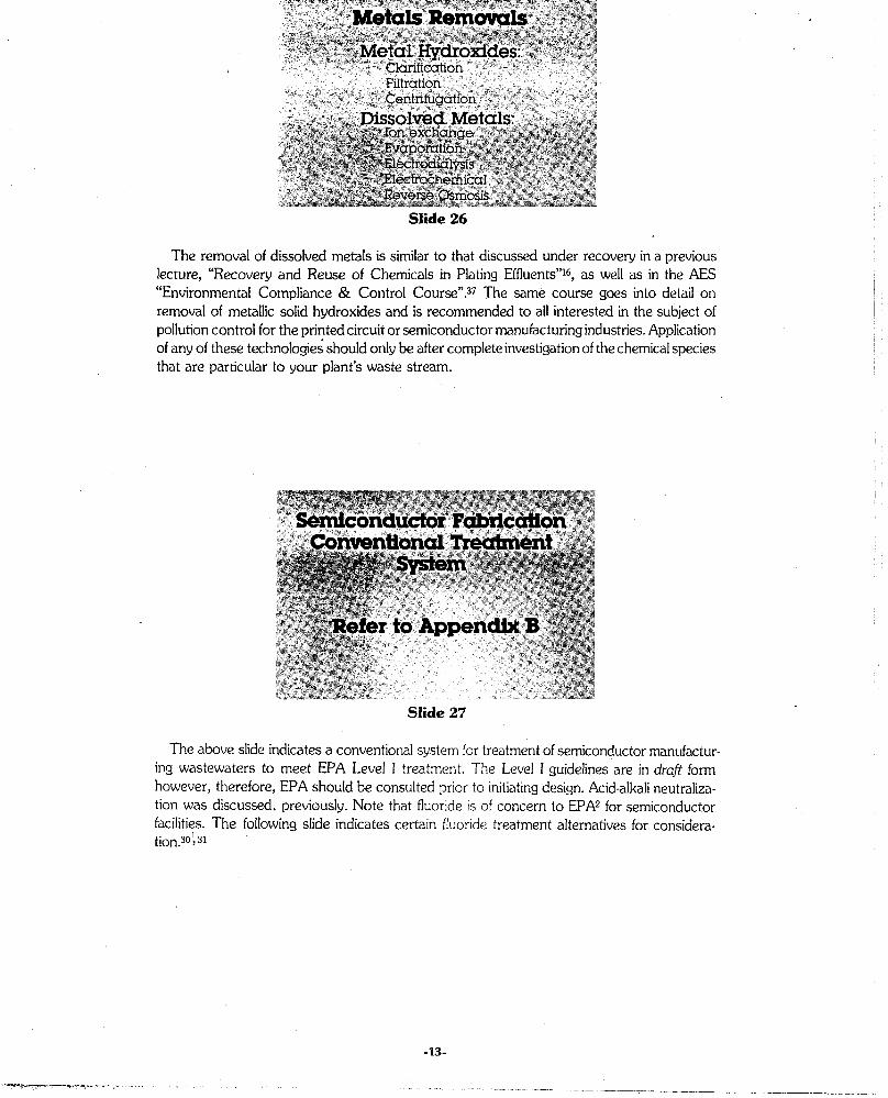
Slide 26
The removal of dissolved metals is similar to that discussed under recovery in a previous lecture, “Recovery and Reuse of Chemicals in Plating Effluents”16, as well as in the AES “Environmental Compliance & Control Course”.37 The same course goes into detail on removal of metallic solid hydroxides and is recommended to all interested in the subject of pollution control for the printed circuit or semiconductor manufacturing industries. Application of any of these technologies should only be after complete investigation of the chemical species that are particular to your plant’s waste stream.
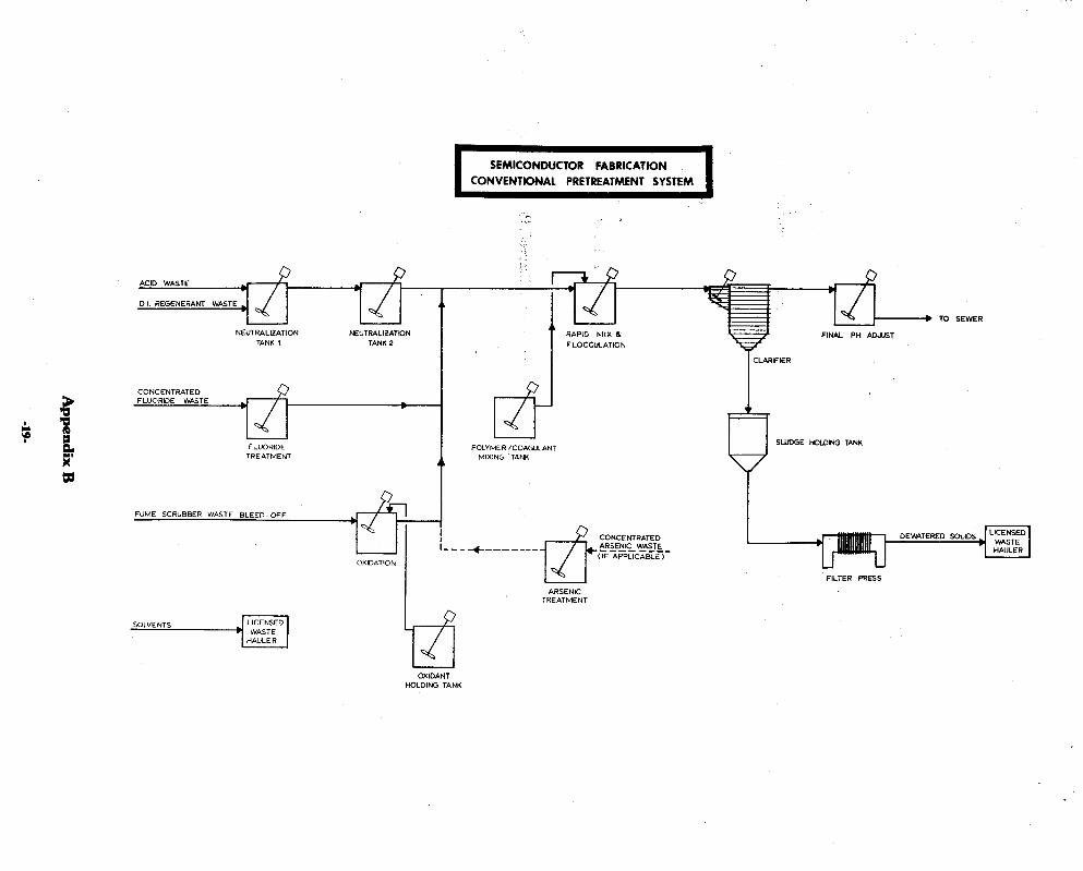
Slide 27
The above slide indicates a conventional system for treatment of semiconductor manufactur- ing wastewaters to meet EPA Level I treatment. The Level I guidelines are in drafl form however, therefore, EPA should be consulted prior to initiating design. Acid-alkali neutraliza- tion was discussed, previously. Note that fluoride is of concern to EPA2 for semiconductor facilities. The following slide indicates certain fluoride treatment alternatives for considera- tion.30: 31

Slide 28
Solvent management has been addressed by P A 2 as shown in the following slide.
Slide 29
The initial thrust by EPA will be collection and hauling of solvents, followed by segregation for recycle and/or reclaim. Finally, EPA may require carbon adsorption of trace organics from the treated effluent waste stream. These guidelines, now draft, will be updated in the near future by the Agency. The treatment methods for both printed circuit and semiconductor wastewaters as discussed, can generate solid sludges to be disposed of. The expense of hauling these waste sludges can be minimized by dewatering the solids as much as possible.
-14-

Slide 30
The centrifuge and the filter press are most often utilized in the electronics industry for dewatering. However, the filter press is currently becoming the more frequently utilized method due to the relatively higher solids (35-50% by weight of solids) concentration that can be obtained and subsequently lower hauling costs.
Slide 31
A diagram of a typical filter press is shown in the above slide, while a typical centrifuge for electronics waste sludge is shown on Slide 32. More detailed information is in the references32,l 3.
-15-

Slide 32
Other factors will impact on the pollution control program which can be considered to be site or facility specific.
Slide 33
The issue of sludge handling and regulatory impacts under the Resource Conservation and Recovery Act (RCRA) has become critical to the electronics industry. As such, the minimiza- tion of sludge water content, utilization of licensed hazardous waste haulers, siting of additional hazardous waste disposal facilities, possible delisting of sludge as a non-hazardous waste (e.g., EP. Toxicity Test under RCRA) are all important considerations. Further information on this subject can be obtained from the references 34, 35, and 36.
-16-

Slide 34
The incorporation of in-line treatment techniques will require floor space within the plating room, while end-of-pipe treatment can utilize more remote space. Utilities available, such as air, steam, electric, water, and ventilation will impact the wastewater treatment (WWT) design. For example, compressed air driven sludge pump could not be used without a source of compressed air, nor could a 48OV electrical motor be operated on a llOV source. Certain managements want to invest more heavily in capital to reduce operating costs, while the reverse can also be true. Local and state regulations will impact WWT design-the regulations can be more stringent than federal, and therefore would take precedence. Whether the effluent will dis- charge to a publicly owned treatment works (POTW)! or directly to a waterway will impact regulations involved and therefore the WWT design basis. The personnel available to operate the WWT system. when it is built or installed should also be considered. Clearly, a highly technical advanced treatment method would not be suitable for unskilled personnel to operate.
Slide 35
The above slides summarizes this lecture. One final recommendation. Many of the i re i l l ,
contained in this overview are detailed at length in the references listed and these should be consulted. In particular, the American Electroplaters’ Society, “Environmental Compliance and Control Course” should be taken by those who want a firm background in achieving the optimum pollution control program for their facility.

I L
d W M I34SNVll d1 d W M dWnS dS 11 3WUd Hd Hd
1 w L
4 4 A A I ' I
I
I 4 J Lcrl
P
Appendix B
-19-

References 1. R. S. Capaccio, Symposium Proceedings-AES 9th Plating in the Electronics Industry,
2. U.S. EPA, “Development Document [or Effluent Limitations and Standardsfor the Electri-
3. U.S. EPA, “Development Document for Effluent Limitations and Pretreatment Standards
4. U.S. EPA. “Environmental Regulation and Technology, The Electroplating Industry”, EPA
5. A. N. Mabbett, “Conference Highlights Reagan Policy on Environmental Matters”, Plating
6 . F. Steward and L. Lancy, “Pollution Abatement Materials Conservation and Recovery”,
7. C. Roy, “Establishing a Program for Pollution Control”, Plating and Surface Finishing, AES,
8. D. A. Swalheim, “Rinsing, Recycle and Recovery of Plating Effluents”, Electronic Intensive
9. J . B. Mohler, “Performance of a Rinsing Tank”, Metal Finishing 21-28 (August & Sep-
10. A. J. Wallace, Jr., ”Solution Dragout & Rinsing After Chromium Plating”, Plating and
11. J. B. Mohler, “Dual Purpose Rinsing”, Plating and Surface Finishing, 48-49, (September,
12. F. A. Lowenheim, Modem Hectroplafing, 3rd edition, John Wiley & Sons, New York, NY,
13. J. E. McNutt, “Electroplating Waste Control”, Plating and Surface Finishing, 16-18, (July,
14. B. Kegel, Ph.D., “Plasma Removal of Drill Smear”, Circuits Manufacturing, 26-30, (March,
15. Staff Report, “Exhibitors at AES Show Amplify Views on Pollution Control”, Plating and
16. J . E. McNutt, D. A. Swalheim, “Recovery and Reuse of Chemicals in Plating Effluents”,
17. R. Heller, “On the Road to Recovery”, Plating and Surface Finishing, 24-25, (June, 1981). 18. R. S. Capaccio, unpublished conference notes, “Outlook ’82”, National Association of
19. L. Atimion, “A Program of Conservation, Pollution Abatement”, Plating and Surface
20. Staff Report, ‘‘Evaporative/Chiller System Recovers Brass Plating Solutio;’,, Plating &
21. R. E. Horn, “Continuous Regeneration of an Electroless Copper Bath”, Plating and Surface
22. U.S. EPA, “In Plant Changes”, EPA 625/8-82-008, (January, 1982). 23. Dr. R. E. Wing, “Treatment for Complexed and Chelated Rinsewaters”, Environmental
24. C. J . Brown, et al., “Recovery of Nitric Acid from Solutions Used for Treating Metal
25. C. F. Coombs, Jr., Editor, Printed Circuits Handbook, 2nd edition. McGraw-Hill, 9-20 to
26. Canning Handbook on Electroplating, 22nd edition, 907-909, (1978). 27. R. L. Moore, Neutralization of Wastewater by pH Control, ISA, 1978. 28. F. G. Shinskey, pH & pIon Control in Process & Waste Streams, John Wiley & Sons,
29. B. C. Lawes, Treatment of Cyanide and Chromate Rinses, AES, 1972. 30. E. G. Paulson, “Reducing Fluoride in Industrial wastewater”, Chemical Engineering, 89-94,
“Wastewater Treatment for the Electronics Industry”, AES (February, 1982).
cal and Electronic Components Point Source Category-Draft”, (Octdber 1980).
for the Electroplating Point Source Category-Final”, (August 1979).
625/10-80oO1, (August, 1980).
and Surface Finishing, 100 (January, 1982).
Metal Finishing, (January-April, 1981).
68,29 (October, 1981).
Training Course, AES.
tember, 1981).
Surface Finishing, 49-51, (November, 1974).
1974).
1974.
1980).
1981).
Surface Finishing, 10-14, (September, 1979).
Electronics Intensive Training Course, an AES Illustrated Lecture.
Metal Finishes Show-Conference, November, 1981.
Finishing, 18-20, (March 1980).
Surface Finishing, 21-29, (January, 1980).
Finishing, 50-52, (October, 1981).
Compliance Control Course, AES, (1980).
Surfaces”, Plating and Surface Finishing, 6062, (February, 1980).
9-21, (1967).
1973.

31.
32
33 r 34
35 36. 37.
(October 17, 1977). D. G. Miller, “Fluoride Precipitation in Metal Finishing Waste Effluent”, 3946, AIChE Symposium Series, Water 1974: I. Industrial Waste Treatment, (1974). R. Crain, “Solids Removal and Concentration”, AES Environmental Compliance and Control Source, AES (1980). R. Heller & C. Roy, “Integrated Treatment Setup Features Sludge-Dewatering Systems”, Plating & Surface Finishing, 22-26, (April, 1980). U.S. EPA, Hazardous Waste Management System, Federal Register, May 19, 1980 pp.
U.S. EPA, “Questions and Answers on Hazardous Waste Regulations: SW-853, 1980. U.S. P A , “Management of Metal Finishing Sludge”, EPA/530/SW-S61, (Feb. 1977). R. E. Wing & W. E. Rayford, “Heavy Metal Removal Using Dithiocarbamates”, Plating and Surface Finishing, 67-71, (January, 1982).
33063-33285.
-21-


