![The influence of Cu-doping on aluminum nitride, silicon ...rms.scu.ac.ir/Files/Articles/Journals/Abstract/1-s2.0-S...The potential usage of Cu-functionalized armchair [4,4] silicon](https://static.fdocuments.in/doc/165x107/60f87e7b24c72f0afd597a42/the-influence-of-cu-doping-on-aluminum-nitride-silicon-rmsscuacirfilesarticlesjournalsabstract1-s20-s.jpg)
Polarization doping: new opportunities for III-nitride ... · 1 Polarization doping: new...
12
1 Polarization doping: new opportunities for III-nitride optoelectronics Sergey Yu. Karpov Workshop “Intensive Discussion on Crystal Growth of Nitride Semiconductors , Sendai, Japan, 22-23 October, 2012 STR Group – Soft-Impact, Ltd (St.Petersburg, Russia)
Transcript of Polarization doping: new opportunities for III-nitride ... · 1 Polarization doping: new...

1
Polarization doping: new opportunities for III-nitride
optoelectronics
Sergey Yu. Karpov
Workshop “Intensive Discussion on Crystal Growth of Nitride Semiconductors , Sendai, Japan, 22-23 October, 2012
STR Group – Soft-Impact, Ltd (St.Petersburg, Russia)

2 Polarization doping for High-Electron Mobility Transistors
AlGaN
GaN
polarization charge (PC) located at
the interface
electron density
distribution
2DEG formation due to
polarization doping
A. Bykhovsky et al., J. Appl. Phys. 74 (1993) 6734 – strong piezoeffect
F. Bernardini et al., Phys. Rev. B 56 (1997) R10024 – spontaneous polarization
at the moment, polarization doping is routinely exploiting in AlGaN/GaN
and AlInN/GaN HEMTs, providing the sheet electron concentration in the
range of ~0.8-2.6××××1013 cm-2
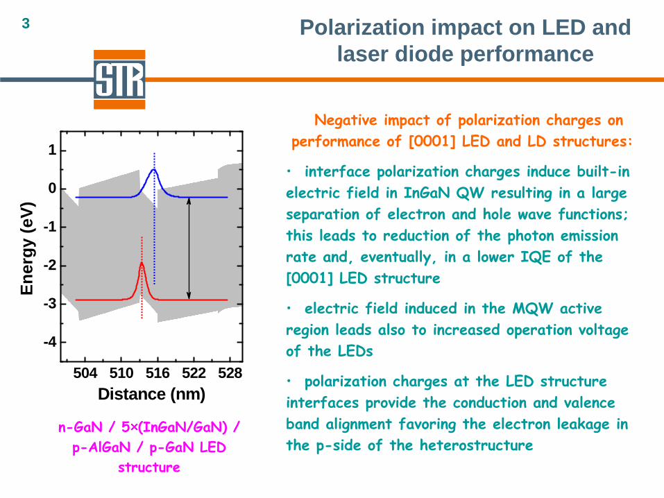
3 Polarization impact on LED and laser diode performance
504 510 516 522 528
-4
-3
-2
-1
0
1 I = 10 mA
2.661 eV
Ene
rgy
(eV
)
Distance (nm)
n-GaN / 5××××(InGaN/GaN) /
p-AlGaN / p-GaN LED
structure
Negative impact of polarization charges on
performance of [0001] LED and LD structures:
• interface polarization charges induce built-in
electric field in InGaN QW resulting in a large
separation of electron and hole wave functions;
this leads to reduction of the photon emission
rate and, eventually, in a lower IQE of the
[0001] LED structure
• electric field induced in the MQW active
region leads also to increased operation voltage
of the LEDs
• polarization charges at the LED structure
interfaces provide the conduction and valence
band alignment favoring the electron leakage in
the p-side of the heterostructure

4 Fundamentals of distributed polarization doping (DPD)
0.3
0.5
0.1
XAlN
0.3
0.5
0.1
XAlN
0.3
0.5
0.1
XAlN
[0001]
[0001]
[0001]
nominal: uniform
composition
graded-down: descending composition
graded-up: ascending
composition
positive PC
negative PC
zero PCgraded-
composition AlGaN
GaN
polarization charge (PC)
zdPd
ρ z−=
Distributed polarization doping (DPD) has been initially proposed
for III-nitride FETs
Experiment: D. Jena et al., Phys.Stat.Solidi (c) 0 (2003) 2339 – n-type DPD
PCs are formed at interfaces
only
p-type DPD
inducing holes
in the material
n-type DPD
inducing electrons
in the material
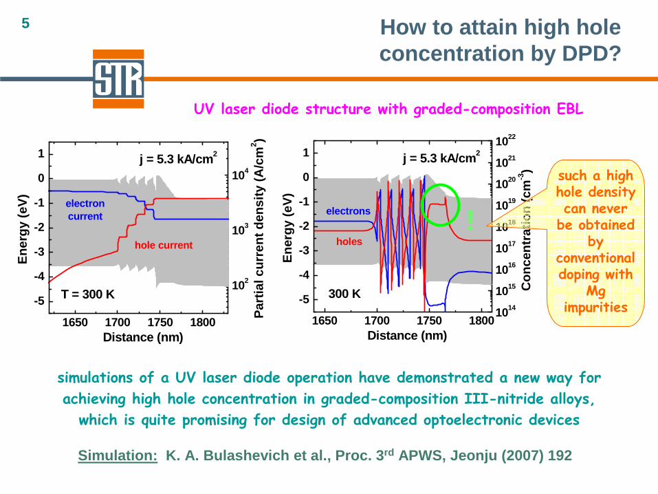
5 How to attain high hole concentration by DPD?
Simulation: K. A. Bulashevich et al., Proc. 3 rd APWS, Jeonju (2007) 192
102
103
104
1650 1700 1750 1800
-5
-4
-3
-2
-1
0
1
electroncurrent
hole current
Ene
rgy
(eV
)
Distance (nm)
T = 300 K
j = 5.3 kA/cm 2
Par
tial c
urre
nt d
ensi
ty (
A/c
m2 )
1014
1015
1016
1017
1018
1019
1020
1021
1022
1650 1700 1750 1800
-5
-4
-3
-2
-1
0
1
electrons
holes
Ene
rgy
(eV
)
Distance (nm)
300 K
j = 5.3 kA/cm 2
Con
cent
ratio
n (c
m-3)
!
such a high hole density can never
be obtained by
conventional doping with
Mg impurities
UV laser diode structure with graded-composition EBL
simulations of a UV laser diode operation have demonstrated a new way for
achieving high hole concentration in graded-composition III-nitride alloys,
which is quite promising for design of advanced optoelectronic devices
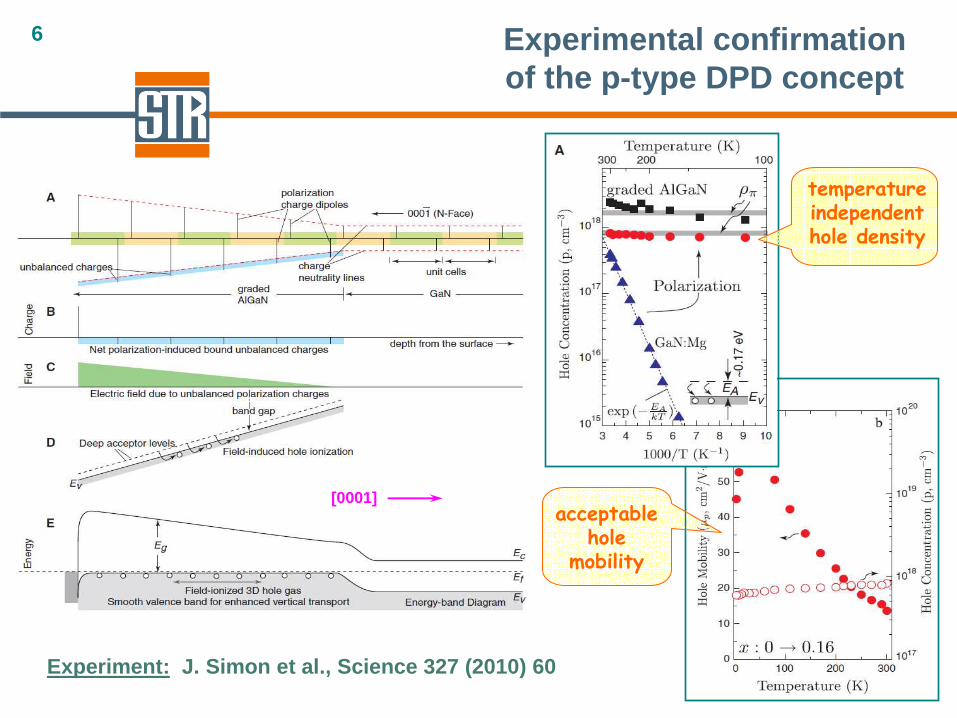
6 Experimental confirmation of the p-type DPD concept
Experiment: J. Simon et al., Science 327 (2010) 60
acceptable hole
mobility
[0001]
temperature independent hole density
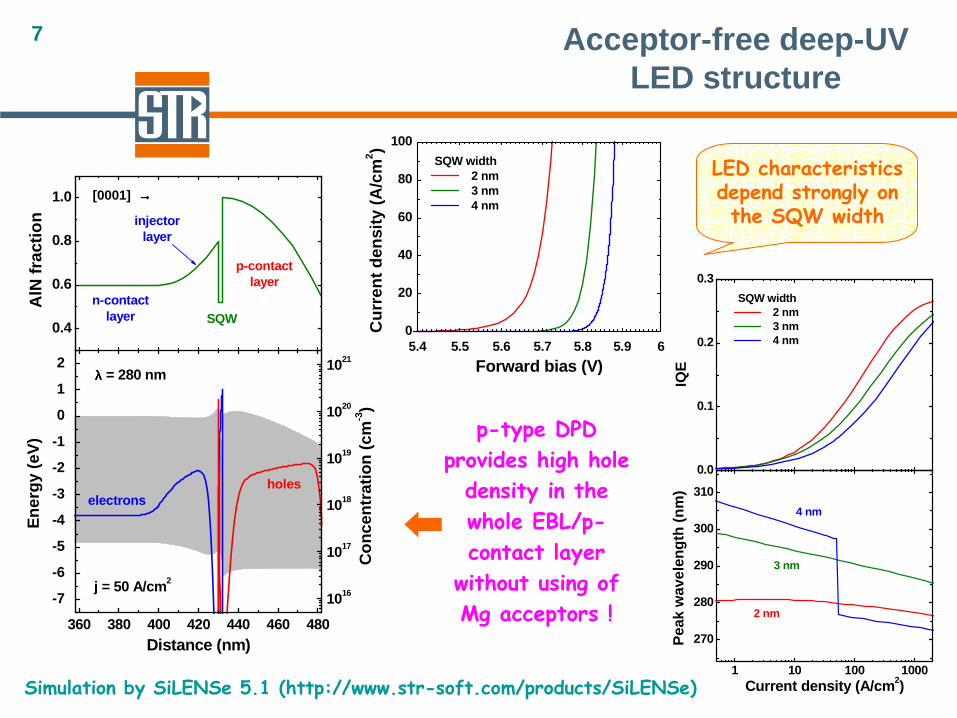
7 Acceptor-free deep-UV LED structure
360 380 400 420 440 460 480
-7
-6
-5
-4
-3
-2
-1
0
1
2λλλλ = 280 nm
holes
Ene
rgy
(eV
)
Distance (nm)
electrons
j = 50 A/cm 2
1016
1017
1018
1019
1020
1021C
once
ntra
tion
(cm
-3)
0.4
0.6
0.8
1.0
injectorlayer
n-contactlayer
AlN
frac
tion
p-contactlayer
SQW
5.4 5.5 5.6 5.7 5.8 5.9 60
20
40
60
80
100
SQW width 2 nm 3 nm 4 nm
Cur
rent
den
sity
(A
/cm
2 )Forward bias (V)
1 10 100 1000
270
280
290
300
310
0.0
0.1
0.2
0.3
4 nm
3 nm
Pea
k w
avel
engt
h (n
m)
Current density (A/cm 2)
2 nm
SQW width 2 nm 3 nm 4 nm
IQE
LED characteristics depend strongly on the SQW width
p-type DPD
provides high hole
density in the
whole EBL/p-
contact layer
without using of
Mg acceptors !
Simulation by SiLENSe 5.1 (http://www.str-soft.com/products/SiLENSe)
[0001] →→→→
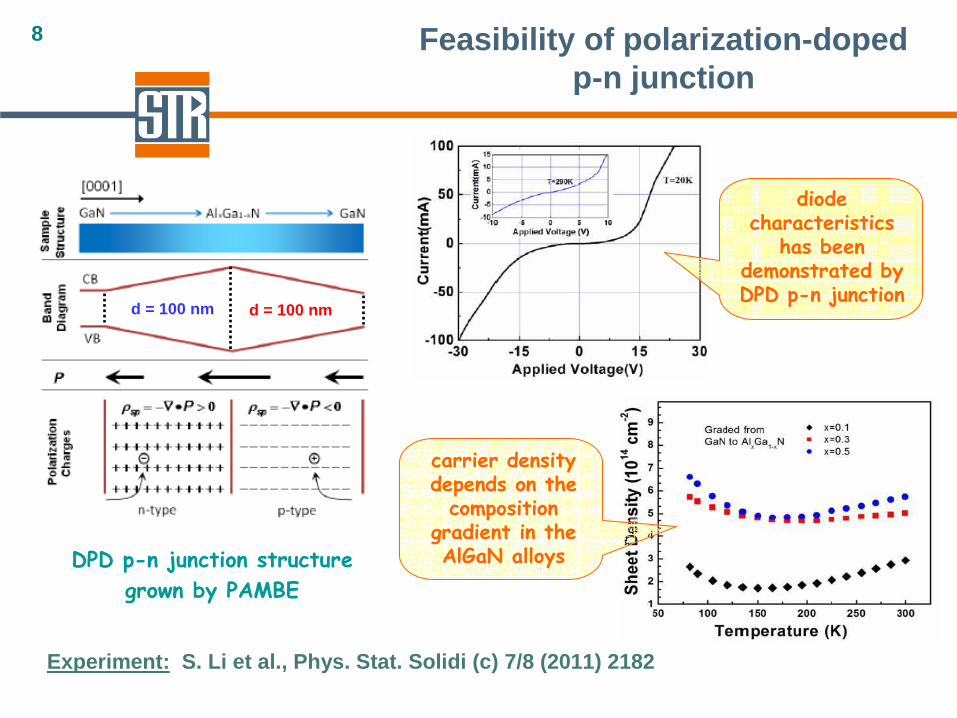
8 Feasibility of polarization-doped p-n junction
Experiment: S. Li et al., Phys. Stat. Solidi (c) 7/8 (2011) 2182
d = 100 nm d = 100 nm
diode characteristics
has been demonstrated by DPD p-n junction
carrier density depends on the
composition gradient in the AlGaN alloysDPD p-n junction structure
grown by PAMBE

9 Feasibility of polarization-doped UV LED structures
Experiment: S. D. Carnevale et al., Nanoletters 12 (2012) 915
deep-UV nanowire LED structures with 7 nm GaN SQW
and 110 nm DPD AlGaN claddings were grown be
PAMBE (with the nanowire diameter of ~25 nm)
both SQW and DPD-AlGaN cladding designs were
far from optimal ones

10 Low -resistance p-type Ohmic contact based on polarization doping
10-4 10-3 10-2 10-1 1001016
1017
1018
1019
1020
1021
modeling experiment :
n-type DPD p-type DPD
Car
rier
conc
entr
atio
n (c
m-3)
Composition gradient (nm -1)
graded AlGaN/GaN
desirableregion
10-4 10-3 10-2 10-1 10010-8
10-7
10-6
10-5
10-4
10-3
DPD AlGaN
Mg-doped GaN & 7%-AlGaN
Con
tact
res
ista
nce
(ΩΩ ΩΩ
·cm
2 )Composition gradient (nm -1)
desirableregion
annealed Ni/Au contacts to graded AlGaN alloys
with the Al content descending along the [0001]
direction from a certain value to zero
Experiment and model: S. Nikishin et al., Appl. Phys. Lett. 95 (2009) 164502100 150 200 250 300 350 400
10-7
10-6
10-5
10-4
10-3
10-2
10-1
100
101
102
Mg doped GaN DPD-AlGaN with
composition gradient of 5x10 -3 nm -1
Con
tact
res
ista
nce
(ΩΩ ΩΩ
·cm
2 )
Temperature (K)

11 Feasibility of Ohmic contacts formed to graded-composition AlGaN
Experiment: S. Li et al., Appl. Phys. Lett. 1018 (2012) 122103
n-contact
p-contact
100 nm graded-composition Al 0.1Ga0.9N
linear I-V characteristics is demonstrated for Ohmic contact to acceptor-free DPD AlGaN
diode characteristics of the DPD AlGaNp-n junction, impurity-doped GaN p-njunction, and GaN Schottky barrier

12Conclusions
simulations show that the use of distributed polarization doping (DPD) provides new opportunities for design of advance optoelectronic devices like LEDs, laser diodes, and solar cells
first experimental studies support the DPD concept in general but they do not utilize in full measure all its advantages, being carried out under conditions far from optimal ones
a prototype of deep-UV LED structure is proposed and examined theoretically; it is found to be quite promising for improving the p-type conductivity in the heterostructure and forming low-resistance p-contacts to the LED
implementation of the DPD concept in the device fabrication technology will require special approaches for precise control of the composition profile and strain relaxation in the device structures during their epitaxial growth