Polariton-polariton interactions in a cavity-embedded 2D-electron gas
This is a repository copy of Polariton states bound to defects in GaAs/AlAs planar microcavities.
White Rose Research Online URL for this paper:http://eprints.whiterose.ac.uk/102115/
Version: Accepted Version
Article:
Zajac, J.M., Langbein, W., Hugues, M. et al. (1 more author) (2012) Polariton states boundto defects in GaAs/AlAs planar microcavities. Physical Review B , 85 (16). 165309. ISSN 2469-9950
https://doi.org/10.1103/PhysRevB.85.165309
[email protected]://eprints.whiterose.ac.uk/
Reuse
Unless indicated otherwise, fulltext items are protected by copyright with all rights reserved. The copyright exception in section 29 of the Copyright, Designs and Patents Act 1988 allows the making of a single copy solely for the purpose of non-commercial research or private study within the limits of fair dealing. The publisher or other rights-holder may allow further reproduction and re-use of this version - refer to the White Rose Research Online record for this item. Where records identify the publisher as the copyright holder, users can verify any specific terms of use on the publisher’s website.
Takedown
If you consider content in White Rose Research Online to be in breach of UK law, please notify us by emailing [email protected] including the URL of the record and the reason for the withdrawal request.

Polariton states bound to defects in GaAs/AlAs planar microcavities
Joanna M Zajac∗ and Wolfgang LangbeinSchool of Physics and Astronomy, Cardiff University,
The Parade, Cardiff CF24 3AA, United Kingdom
Maxime Hugues and Mark HopkinsonDepartment of Electronic and Electrical Engineering,
University of Sheffield. Mappin Street, Sheffield S1 4JD, UK
(Dated: January 8, 2014)
We report on polariton states bound to defects in planar GaAs/AlAs microcavities grown bymolecular beam epitaxy. The defect types relevant for the spatial polariton dynamics in these struc-tures are cross-hatch misfit dislocations, and point-like defects extended over several micrometers.We attribute the latter defects to Ga droplets emitted occasionally by the Ga cell during the growth.These defects, also known as oval defects, result in a dome-like local modulation of surface, whichis translated into the cavity structure and leads to a lateral modulation of the cavity polaritonenergy of up to 15 meV. The resulting spatially localized potential landscape for the in-plane polari-ton motion creates a series of bound states. These states were characterized by spectrally resolvedtransmission imaging in real and reciprocal space, and reveal the spatial potential created by thedefects. Interestingly, the defect states exhibit long lifetimes in the 10 ps range, which we attributeto a spatially smooth confinement potential.
I. INTRODUCTION
Semiconductor microcavities have been extensivelystudied in last 20 years1–3. Significant attention wasgiven to planar microcavities, which are Fabry-Perot res-onators, with a photon mode confined in growth directionby Bragg mirrors made of pairs of λ/4 layers of alter-nating refractive index. The in-plane dispersion of themode is close to quadratic for in-plane wavevectors kmuch smaller than the free-space wavevector, with a cur-vature described by an effective mass about 4 orders ofmagnitude smaller than the free electron mass. This im-plies a significant dispersion within the external opticallyaccessible wavevector range. When coupled to a quan-tum well exciton, these microcavities allow to investigatefundamental condensed-matter phenomena like strongcoupling, Bose-Einstein condensation, lasing, paramet-ric amplification, etc. In many cases, these effects aresignificantly affected by the disorder in the structures.This leads to localization of the Bose-Einstein conden-sate, formation of vortices and can be used as a probefor the dynamics and excitations the polaritonic super-fluid phase4–6.
The spatial localization of the cavity mode by artifi-cial in-plane structures was investigated experimentallyand theoretically in Refs. 7–11. In these works, circu-lar mesas with diameters of 3-19µm and heights in thenanometer range were created by lithography on the cav-ity layer before growing the top Bragg mirror.
In nominally planar samples it is typically observedthat the cavity mode is elastically scattered on a cross-hatched dislocation pattern12–16, while the excitonic parttends to exhibit a more isotropic disorder on the relevantmicrometer length scale. In samples grown by MOCVD,additional random disorder is observed, indicating a fluc-tuation of the layer thickness in the micrometer spatialrange due to the growth mode influenced by transportof the reactants via the gas-phase, allowing for non-homogeneous deposition. In MBE instead, the molecular
beam guarantees the random deposition of Ga atoms,and the surface diffusion, which is limited to typically100 nm, cannot create a long-range thickness modulation.
Apart from the cross-hatch dislocation pattern, onetypically observes point-like defects (PD) with a sur-face density of about 104/cm2, which have a size andshape typical of those ascribed as oval defects17. PDsare better visible in the regions of lower density of cross-hatches, however were observed in all regions, and fordifferent MC samples which we investigated until now.They are not related to strain relaxation, but are gener-ally attributed to particle contamination during growthor Ga source spitting18. These defects produce ratherextended surface modulations, typically without latticedefects. Polariton modes in MCs have typical extensionsof 10-100 micrometers, limited by mirror transmissionor residual disorder. These modes are therefore sensi-tive to the length-scale of the PDs, making an excellentprobe for structure inhomogeneities in the 1-100 microm-eter range. The resonant local transmission of the MC ismodified by the PDs, creating spatially confined cavitymodes, typically visible as a series of spectrally narrowlocalized modes, as will be shown here. The paper is or-ganized as follows. In Section II the details of the samplesand the experiment are given, followed by a descriptionof the disorder inside these structures in Section III, anda presentation of the results of the optical measurementson localized states in Section IV. The origin of PDs isdiscussed in Section V.
II. SAMPLE AND EXPERIMENT
The sample investigated in this work is a bulk 1λc
GaAs semiconductor microcavity (MC) surrounded byAlAs/GaAs distributed Bragg reflectors (DBRs) with 27(24) λc/4 pairs on the bottom (top), respectively. Imagesof a sample are shown on Fig. 1. At a temperature ofT=80 K, the cavity mode energy was EC = 1.485 eV,
arX
iv:1
111.
6012
v1 [
cond
-mat
.mtr
l-sc
i] 2
5 N
ov 2
011

2
2 µm
FIG. 1: Scanning electron micrograph of the studied micro-cavity (left), and sketch of the sample structure (right) show-ing examples of defects, starting from different layers acrossthe structure.
red detuned by 23 meV from the bulk GaAs exciton inthe cavity layer at 1.508 eV. The structure was grownunder continuous wafer rotation, resulting in a very weak(<1%) thickness variation from the center to the edge ofthe wafer.
The optical measurements of the polariton states wereconducted at nitrogen temperature (T=80 K) with thesample mounted strain-free in a bath cryostat. Real andreciprocal space transmission spectra were taken in thelow-intensity regime. A sketch of the setup is shown onFig. 2.
Two different optical excitation configurations wereused. Firstly, a single-mode external cavity diode laser(Sacher Lynx) with 5MHz linewidth was employed toexcite the polaritons at normal incidence (k = 0) overa large size in real space (∼ 1mm) from the substrateside. This excitation allowed to selectively image a spe-cific polariton energy with a spectrally integrating detec-tor. Secondly, a mode-locked Ti:Sapphire laser (CoherentMira) was used providing 100 fs pulses at 76 MHz repe-tition rate. The large spectral width of approximately20 meV allows to excite polariton bound states and thecontinuum dispersion simultaneously. The excitation wasspatially focussed to a spot of about 3µm diameter us-ing a lens of 0.15 numerical aperture, corresponding toan excitation wavevector range of |k| < 1.1/µm. Theemission was collected from the epi-side by an asphericlens of 0.5 NA (L3 in Fig. 2) with a wavevector range of|k| < 4/µm, providing a spatial resolution of about 1µm.The emission was detected spectrally integrated in thereal or reciprocal space using video CCD cameras. Forspectrally resolved detection, the emission was imaged inreal or reciprocal space into the input slit of an imag-ing spectrometer with 12µeV spectral resolution. Two-dimensional images were acquired by translating the im-age across the spectrometer slit using lateral movementsof two lenses (LS1 and LS2 in Fig. 2). Scans were madewith 0.5µm (real space), or 0.05µm−1 (reciprocal space)steps.
Laser
PH
CCD
Bath Cryostat
MC
L3
LS1
LS2
L4L1 L2
M1
Spectrometer & CCD
L5
FIG. 2: Sketch of the optical setup used to measure the lo-calized polariton states. Both real-space and reciprocal spaceimaging was used. L1-L5 Lenses, MC: Microcavity sampleLS1,LS2 moving lenses for imaging, for details see text.
III. DISORDER VARIATION VERSUS
GROWTH TEMPERATURE
During the growth of the investigated structure, thetemperature was ramped up to 715 ◦C for the AlAs lay-ers, and down to 660◦C for the Bragg GaAs layers, andto 630◦C for the GaAs cavity layer. For comparison,in Ref. 19 the sample was grown at a constant tempera-ture of 620−630◦C. A radial non-uniformity of the back-surface roughness due to As evaporation and resultingGa-droplet formation was observed (see Fig. 3g). Thisindicates that the growth temperature was non-uniformacross the wafer, an effect which is significant due to theusage of an undoped and back-side polished 3-inch wafer,leading to a weaker radiative coupling to the surround-ing compared to doped wafers, increasing the infrared ab-sorption, and unpolished wafers, decreasing the reflectionand avoiding radiation trapping by total-internal reflec-tion. The cavity resonance energy was varying by only0.5 % over the wafer, indicating an exceptional flux ho-mogeneity of the Ga and Al cells. The polariton disorderinstead was found to vary significantly as function of ra-dial position R on the wafer, as shown in Fig. 3a)-f) wheretransmission images and spectra are shown at differentR. Close to the center (R = 4mm), a cross-hatch patternis visible and the polariton states excited at k = 0 showan inhomogeneous broadening of ∼ 100µeV. This cross-hatch disorder decreases with increasing radius, and isnot discernible at R = 32mm close to the edge of thewafer. The cross-hatch pattern is due to the formationof a misfit-dislocation pattern found in (001) orientedstrained cubic semiconductor thin film systems20. It isformed by strain relaxation via slides along the {111}slip planes, which form lines along [110] and [11̄0] attheir intersection with the film surface. Such a pattern isonly observed for weakly strained films (ǫ < 2%), whilefor higher strains Stranski-Krastanov or Volmer-Webergrowth is found. Cross-hatch patterns are typically re-ported for a lattice mismatch of the order of 1%, leadingto a large density of slip lines and a significant surfacemodulation of several nanometers. The lattice mismatchof the GaAs/AlAs Bragg mirrors at room temperature21
is 0.14%. Using a mismatch of 0.07% of a Bragg pe-riod, we find a critical thickness for strain relaxation22
3
0 1
b)
x (mm)
22 mm radius
0 1
c)
4 mm radius
1.4848 1.48520
1d)
y (m
m)
1.4800 1.4804 1.4808
e)
energy(eV)1.4848 1.4852
f)
0 10
1 y
(m
m)
32 mm radius
a)
0 10
1h)
32 mm radius
y (m
m)
x (mm)0 300
30
g)
y (m
m)
x (mm)
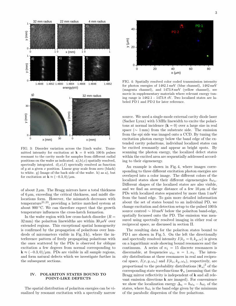
FIG. 3: Disorder variation across the 3 inch wafer. Trans-mitted intensity for excitation at k = 0 with 100 fs pulsesresonant to the cavity mode for samples from different radialpositions on the wafer as indicated. a),b),c) spatially resolved,spectrally integrated. d),e),f) spectrally resolved as functionof y at a given x position. Linear gray scale from zero (black)to white. g) Image of the back side of the wafer. h) as a), butfor excitation at k ≈ (−0.3, 0)/µm.
of about 2µm. The Bragg mirrors have a total thicknessof 6µm, exceeding the critical thickness, and misfit dis-locations form. However, the mismatch decreases withtemperature21,23, providing a lattice matched system atabout 900 ◦C. We can therefore expect that the growthtemperature influences the cross-hatch formation.
In the wafer region with low cross-hatch disorder (R =32mm) the polariton linewidths are within 30µeV overextended regions. This exceptional spatial homogeneityis confirmed by the propagation of polaritons over hun-dreds of micrometers visible in Fig. 3 h), where the in-terference pattern of freely propagating polaritons withthe ones scattered by the PDs is observed for obliqueexcitation a few degrees from normal corresponding tok ≈ (−0.3, 0)/µm. PDs are visible in all sample regions,and form natural defects which we investigate further inthe subsequent sections.
IV. POLARITON STATES BOUND TO
POINT-LIKE DEFECTS
The spatial distribution of polariton energies can be vi-sualized by resonant excitation with a spectrally narrow
0 20 40 60 800
20
40
y (µ
m)
x (µm)
PD 2
PD 1
FIG. 4: Spatially resolved color coded transmission intensityfor photon energies of 1482.1meV (blue channel), 1482meV(magenta channel), and 1473.8meV (yellow channel), seemovie in supplementary materials where relevant energy tun-ing range is 1482.1 - 1473.8 eV. Two localized states are la-beled PD 1 and PD 2 for later reference.
source. We used a single-mode external cavity diode laser(Sacher Lynx) with 5 MHz linewidth to excite the polari-tons at normal incidence (k = 0) over a large size in realspace (∼ 1mm) from the substrate side. The emissionfrom the epi side was imaged onto a CCD. By tuning theexcitation photon energy below the band edge of the ex-tended cavity polaritons, individual localized states canbe excited resonantly and appear as bright spots. Byscanning the photon energy, the localized defect stateswithin the excited area are sequentially addressed accord-ing to their eigenenergy.
An example is shown in Fig. 4, where images corre-sponding to three different excitation photon energies areoverlayed into a color image. The different colors of thelocalized states show their different eigenenergies h̄ωn.Different shapes of the localized states are also visible,and we find an average distance of a few 10µm of thePDs with localized states separated by more than 1 meVfrom the band edge. To gain more detailed informationabout the set of states bound to an individual PD, wechange excitation and detection setup to the pulsed 100 fssource centred ∼ 10meV below the polariton band-edge,spatially focussed onto the PD. The emission was mea-sured using spectrally resolved imaging in either real orreciprocal space, as discussed in section II.
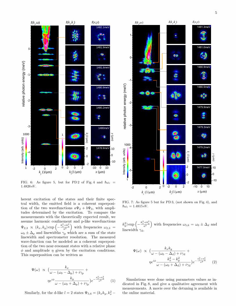
The resulting data for the polariton states bound toPD 1 are shown in Fig. 5. On the left the directionallyand spectrally resolved intensity I(kx = 0, ky, ω) is givenon a logarithmic scale showing bound resonances and thecontinuum. A series of n1 = 15 discrete resonances isdiscernable, at frequencies ωn, n = 1..n1. The inten-sity distributions at these resonances in real and recipro-cal space, I(x, y, ωn) and I(kx, ky, ωn), respectively, are
proportional to the probability distributions |Ψn|2
of thecorresponding state wavefunctions Ψn (assuming that theBragg mirror reflectivity is independent of k and all rele-vant emission directions k are imaged). For conveniencewe show the localization energy ∆n = h̄ωn − h̄ωc of thestates, where h̄ωc is the band edge given by the minimumof the parabolic dispersion of the free polaritons.

4
-2 0 2
-12
-10
-8
-6
-4
-2
0
2
1000
Inte
nsity
(ar
b. u
nits
)
ky (1/µm)
rela
tive
phot
on e
nerg
y (m
eV)
I(x,y)I(kx,k
y)I(k
y,ω)
-2 0 2-2
0
2
y (µm)
ky (1/µm
)
1k
x(1/µm)
1
0
I(x,y)
-10 0 10
-10
0
101471.4meV
1482.1meV
1482.0meV
1481.6meV
1481.2meV
1481.2meV
1480.2meV
1480meV
1479.5meV
1479.3meV
1478.4meV
1477.5meV
x (µm)
1475.7meV
1482.8meVFIG. 5: Spectral imaging of the emission from polaritonstates close to PD 1 of Fig. 4 in real and reciprocal space.Left: intensity I(kx = 0, ky, ω) on a logarithmic color scale asindicated. The energy h̄ω is shown relative to the polaritonband edge at h̄ωc = 1.4833 eV. The intensity of the individualstates is given in reciprocal space I(kx, ky, ωn) in the mid-dle column and in real space I(x, y, ωn) in the right column.They are shown using a linear color scale and are individuallynormalized to their maximum. The resonance energies h̄ωn
are given, and the connection lines indicate the correspondingstate in I(kx = 0, ky, ω). The tails visible in I(x, y, ωn) aredue to imaging abberations relevant at large k.
The ground state Ψ1 is observed at ∆1 = −11.9meV.Some resonances are observed even above the contin-uum, indicating the presence of a potential barrier be-tween the defect region and the surrounding continuum.These states could lead to resonant scattering similar toFeshbach resonances observed in atomic physics. Theshapes of the wavefunctions reveal a nearly cylindricalsymmetry of the effective confinement potential V1(x, y)created by PD1. The first excited state Ψ2 is found at∆2 = −7.6meV, and shows a px-like symmetry, with anode at x = 0. Ψ3 has ∆3 = −5.8meV and a py-likesymmetry with a node at y = 0. The energy splitting ofΨ2,3 shows a breaking of cylindrical symmetry of V1(x, y).The next 3 states correspond to d-states, Ψ4 having zeroangular momentum and 2 nodes in radial direction, andΨ5,6 being superpositions of angular momentum 2. Thenon-degeneracy of the different n=2 states shows the non-parabolicity of the confinement. The higher states canbe classified in a similar way with increasing number ofnodes in the wavefunction.
PD 2 instead is not cylindrically symmetric as shown inFig. 6. The two lowest states Ψ1,2 are separately localizedto the left and the right of the defect center with a s-like wavefunction, indicating two separate minima of thepotential. The left minimum confines also a p-like excitedstate Ψ3, while the corresponding excited state on theright Ψ4 is already extended along a horseshoe-shapedregion, coupling to a d-like state of the left minimum.The next state Ψ5 is a mixture of the left f-like statewith the right d-like state. Ψ6 is mostly localized on thetip of the horseshoe, possibly due to a local potentialmaximum close to the state energy, which is supportedby the relatively small wavevector spread in kx. A totalof n3 = 11 states are visible.
The last reported defect, PD3 (see in Fig. 7, not shownin Fig. 4) is similar to PD1 in being approximately cir-cular symmetric, but about a factor of 3 shallower. Theground state Ψ1 is s-like, and shows a larger extensionin real space and a smaller in reciprocal space than theground state of PD1, as expected from the weaker con-finement. A total of n3 = 12 states are visible.
A. Coherent wavepacket dynamics
The two p-like excited states Ψ2,3 of PD 3 are nearlydegenerate (≈ 100µeV separation). Due to the co-
5
-2 0 2
-4
-3
-2
-1
0
Inte
nsity
(ar
b. u
nits
)
ky (1/µm)
rela
tive
phot
on e
nerg
y (m
eV)
1000
1 -2 0 2-2
0
2
I(kx,k
y) I(x,y)I(k
y,ω)
ky (1/µm
)
kx(1/µm)
-10 0 10
-10
0
10
1
y (µm)
x (µm)
1482.1meV
1481.9meV
1481.6meV
1480.9meV
1480.2meV
1480meV
1478.9meV
0
FIG. 6: As figure 5, but for PD 2 of Fig. 4 and h̄ωc =1.4826 eV.
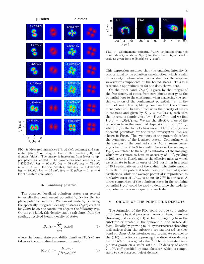
herent excitation of the states and their finite spec-tral width, the emitted field is a coherent superposi-tion of the two wavefunctions aΨ2 + bΨ3, with ampli-tudes determined by the excitation. To compare themeasurements with the theoretically expected result, weassume harmonic confinement and p-like wavefunctions
Ψ2,3 ∝ (kx, ky) exp(
−k2x+k2
y
a2
)
with frequencies ω2,3 =
ω0 ±∆p and linewidths γp which are a sum of the statelinewidth and spectrometer resolution. The measuredwave-function can be modeled as a coherent superposi-tion of the two near-resonant states with a relative phaseφ and amplitude η given by the excitation conditions.This superposition can be written as
Ψ(ω) ∝( kxω − (ω0 −∆p) + iγp
+
ηeiφky
ω − (ω0 +∆p) + iγp
)
e−k2x+k2
y
a2 (1)
Similarly, for the d-like l = 2 states Ψ5,6 = (kxky, k2x −
�� � �
��
�
�
�
�
�������� ���������
����������
������
��� �������
��������
��� � ��
���
�
��
�����������������
��ω�
������
���������
���������
���������
���������
���������
���������
���������
���������
�
����
�� � �
��
��
��
��
��
�
�
����������� � ������!�� ����
FIG. 7: As figure 5 but for PD 3, (not shown on Fig. 4), andh̄ωc = 1.4815 eV.
k2y) exp(
−k2x+k2
y
a2
)
with frequencies ω5,6 = ω0 ± ∆d and
linewidth γd,
Ψ(ω) ∝( kxkyω − (ω0 −∆d) + iγd
+
ηeiφk2x − k2y
ω − (ω0 +∆d) + iγd
)
e−k2x+k2
y
a2 (2)
Simulations were done using parameters values as in-dicated in Fig. 8, and give a qualitative agreement withmeasurements. A movie over the detuning is available inthe online material.
6
1.48049eV
-2 0 2
-2
0
2
d-states
E = 1.47926 eV1.47924eV
1.47922eV
k y (1/
µm)
kx (1/µm)
1.47927eV
1.4793eV
1.47934eV
1.47926eV
1.4805 eV
1.48051 eV
1.48053 eV
1.48054 eV
1.48057eV
p-states
FIG. 8: Measured intensities I(k, ω) (left columns) and sim-ulated |Ψ(ω)|2 for energies close to the p-states (left) andd-states (right). The energy is increasing from lower to up-per panels as labeled. The parameters used were h̄ω0 =1.479205 eV, h̄∆ = 90µeV, h̄γ1 = 58µeV, h̄γ2 = 73µeV,η = 1, φ = 0 for the p-states, and h̄ω0 = 1.48047 eV,h̄∆ = 89µeV, h̄γ1 = 37µeV, h̄γ2 = 50µeV,η = 1, φ = 0for the d-state simulation.
B. Confining potential
The observed localized polariton states can relatedto an effective confinement potential Vm(r) for the in-plane polariton motion. We can estimate Vm(r) usingthe spectrally integrated density of states Dm(r) createdby Vm(r) below the continuum edge in the following way.On the one hand, this density can be calculated from thespatially resolved bound density of states
Dm(r) =
nm∑
n=1
|Ψn(r)|2 (3)
where the bound state probability densities |Ψn(r)|2 are
taken as the normalized measured intensity
|Ψn(r)|2 =
I(r, ωn)∫
I(r, ωn)dr2(4)
��� � ��
���
�
��
�
������
������
���
��� � ��
�
���
��� � ��
�
���
����
FIG. 9: Confinement potential Vm(r) estimated from thebound density of states Dm(r) for the three PDs, on a colorscale as given from 0 (black) to -2.3meV.
This expression assumes that the emission intensity isproportional to the polariton wavefunction, which is validfor a cavity lifetime which is constant for the in-planewavevector components of the bound states. This is areasonable approximation for the data shown here.
On the other hand, Dm(r) is given by the integral ofthe free density of states from zero kinetic energy at thepotential floor to the continuum when neglecting the spa-tial variation of the confinement potential, i.e. in thelimit of small level splitting compared to the confine-ment potential. In two dimensions the density of statesis constant and given by D2D = m/(2πh̄2), such thatthe integral is simply given by −Vm(r)D2D, and we findVm(r) = −D(r)/D2D. We use the effective mass of thepolaritons from the measured dispersion m = 2 ·10−5 me,where me is the free electron mass. The resulting con-finement potentials for the three investigated PDs areshown in Fig. 9. The symmetry of the potentials reflectthe symmetry of the localized states. Comparing withthe energies of the confined states, Vm(r) seems gener-ally a factor of 2 to 3 to small. Errors in the scaling ofVm(r) are related to the length calibration of the imaging,which we estimate to have an accuracy of 10%, yieldinga 20% error in Vm(r), and to the effective mass m whichwe estimate to have an error of 10%, resulting in a totalof 30% systematic error of the scaling. The finite amountof levels in the potential leads mostly to residual spatialoscillations, while the average potential is reproduced toa relative error of 1/nm, so about 10-20% in our case. Adirect comparison of the polariton states in the confiningpotential Vm(r) could be used to determine the underly-ing potential in a more quantitative fashion.
V. ORIGIN OF THE POINT-LIKE DEFECTS
The formation of the PDs could be due to a varietyof different physical processes. Among them, there arethreading dislocations(TD), either propagating from thesubstrate or created in the epilayers due to surface de-fects. Usually by growing multilayer structures threadingdislocations from the substrate are suppressed as theybend on GaAs/AlAs interfaces and propagate parallel tothe 〈110〉 directions suppressing the dislocation densityeven to 5% of its original value24. The investigated sam-ple was grown on a wafer with a TD density of about2 · 103/ cm2 specified by manufacturer, which is compa-rable to the observed defect density.

7
In order to investigate if the observed PD are re-lated to threading dislocations, we used an etchingprocedure25,26, which requires less equipment and sam-ple preparation as compared to the alternative method oftransmission electron microscopy. It also allows to inves-tigate large surface areas, which is necessary consideringthe small defect density. Since the sample is not de-stroyed in the process, it is possible to spatially correlatethe etched pits corresponding to the treading dislocationswith the PDs. We used the procedure described in Ref. 25for GaAs etching of {100} crystal facets. The samplewas kept in KOH etch at 360 oC for 2 minutes. The re-sulting etch-pits on the sample surface were observed ina reflective DIC (Differential interference contrast) opti-cal microscope. We found an etch-pit density of about103/ cm2, consistent with the manufacturer specification.An overview of several defects obtained using DIC mi-croscopy is shown in figure Fig. 10. Each rectangular etchpit marks a threading dislocations in its center. The linesare scratches on the sample surface and/or misfit dislo-cations.
Subsequently the low temperature transmission mea-surements were repeated together with reflection mi-croscopy. The positions of the PDs were found to benot correlated to the etch-pits. Instead, the PDs coin-cide with the round to oval structures of 7-10 micrometerdiameter on the sample surface, as observed in Fig. 10.These defects are thus the origin of the localization po-tentials for the polaritons.
From the DIC images, we have quantitatively ex-tracted the surface profile of the PDs. They show a typi-cal surface height modulation of several tens of nanome-ters, being approximately parabolic with a small depres-sion about 10% of the height below the original surfaceat the edge, and a width of a few µm. The energy bar-rier to the continuum observed in the localized states (seeSection IV) is likely to be related to this edge depression.
Also atomic force microscopy images of the surfacewere obtained, but due to the large extension and smallheight of the PDs no reliable results of the large scaletopology could be extracted.
Using field emission scanning electron mi-croscopy(FESEM), the structures were imaged undergrazing angle of incidence (70◦ to the surface normal) toenhance the contrast for the flat surface topology, andresults are shown in Fig. 10. The shape is consistentwith the DIC images. A ridge shaped structure close tothe center of the dome is also visible.
Growth related defects were categorized in Ref. 18,showing some defects which qualitatively resemble theones discussed here. We observed defects with differentshapes, with the most common being nearly round de-fects with a weak ridge in the center, as shown on Fig. 10.According to Ref. 18 round defects with nucleus origi-nate from Ga oxide or spitting, while obscure ovals arisefrom Ga droplets, oxides or particle contaminants. Weattribute the observed defects to Ga nano-droplets emit-ted by the the Ga cell during growth. Once depositedon the surface, the Ga is converted to GaAs, forming ahill with a depression in the center due to the growthkinetics. During the subsequent growth, lateral Ga dif-
���
�
��
�����
����� ��� ����������
� �����
���
���
�
��
��
��
�
��
�����
�����
������ ��� ����������
������
���
���
�
��
��
�����
����� ��� ����������
�
������ �
�
�������� ��� �������������������
������� ����
��� ����!
FIG. 10: Top: Sample surface after KOH etching imaged withDIC. Round defects corresponding to PDs are labeled. Belowon the left column,individual height profiles of PDs obtainedusing DIC with the corresponding DIC images. In the rightcolumn, corresponding FESEM images of the PDs.
fusion leads to an extension of the hill while its height isreduced. Interestingly, we observe nearly round defectsin the present sample, while on similar samples grownthroughout at a lower temperature of 630◦C similar de-fects are observed, which are elliptical with an about 1:3ratio of extension in the [110] to [11̄0] directions. Weattribute this observation to the temperature-dependentanisotropic Ga mobility on the surface.
Clearly the impact of such a structure on the polari-tons depends on the position of the Ga droplet deposi-tion within the MC structure in growth direction. Thisinformation is not accessible in the characterization tech-niques reported here, which are all measuring the surfacetopology of the structure. To investigate this further,we used combined focussed ion beam (FIB) - scanningelectron beam (SEM) to cut with FIB into the structureand measure the exposed side-wall by SEM27. By se-quentially slicing the structure, a volume information onthe defect is obtained. The results of this investigationincluding a study on the their influence of the dropletpositions relative to the cavity layer on polariton con-finement will be reported in a forthcoming work.

8
VI. SUMMARY
In summary, we have identified point-like defects inplanar microcavities which lead to series of spectrallysharp localized polariton states. The localized polari-ton states were characterized in real and reciprocal spaceand the underlying confinement potential has been re-constructed from these measurements. The symmetry ofthe states can be very close to cylindrical. The origin ofthe defects is attributed to spitting of the Ga cell duringMBE growth, depositing Ga droplets of a size of the orderof 100 nm onto the sample surface during growth. Due tothe large thickness of microcavity structures, the surfacedensity of these droplets is enhanced, and the spatiallyextended polariton states are exceptionally sensitive tothe resulting extended structural variations. The inducedconfinement potential can be rather smooth, allowing for
confined states of small linewidth since the scattering intothe lossy microcavity modes at high wavevectors is sup-pressed.
Acknowledgments
We thank A. Drevisi and I. Fallis for assistance with theKOH etching. This work was supported by the EPSRCUK Research Council (grant n. EP/F027958/1). Authorcontributions: WL designed the samples, MH and MHgrew the samples at the EPSRC National Centre for III-VTechnologies, Sheffield, UK, and gave feedback on sampledesign, JZ performed the structural measurements, JZand WL performed the optical measurements, analyzedthe data and prepared the manuscript.
∗ Electronic address:[email protected] A. Kavokin, J. J. Baumberg, G. Malpuech, and F. P.
Laussy, Microcavities (OUP Oxford, 2007).2 A. Q. B. Deveaud-Plédran and P. Schwendimann, eds.,
Quantum Coherence in Solid State Systems, vol. 171 ofInternational School of Physics Enrico Fermi (IOS Press,2009).
3 M. S. Skolnick, T. A. Fisher, and D. M. Whittaker, Semi-cond. Sci. Technol. 13, 645 (1998).
4 J. Kasprzak, M. Richard, S. Kundermann, A. Baas,P. Jeambrun, J. Keeling, F. Marchetti, M. H. Szymańska,R. André, J. Staehli, et al., Nature 443, 409 (2006).
5 K. G. Lagoudakis, M. Wouters, M. Richard, A. Baas,I. Carusotto, R. André, D. L. S. Dang, and B. Deveaud-Pledran, Nature Physics 4, 706 (2008).
6 A. Amo, J. Lefrère, S. Pigeon, C. Adrados, C. Ciuti,I. Carusotto, R. Houdré, E. Giacobino, and A. Bramati,Nature Physics 5, 805 (2009).
7 R. I. Kaitouni, O. E. Daïf, A. Baas, M. Richard, T. Paraiso,P. Lugan, T. Guillet, F. Morier-Genoud, J. D. Ganière,J. L. Staehli, et al., Phys. Rev. B 74, 155311 (2006).
8 P. Lugan, D. Sarchi, and V. Savona, phys. stat. sol. (c) 3,2428 (2006).
9 R. Cerna, D. Sarchi, T. K. Paraïso, G. Nardin, Y. Lèger,M. Richard, B. Pietka, O. E. Daif, F. Morier-Genoud,V. Savona, et al., Phys. Rev. B 80, 121309(R) (2009).
10 R. Cerna, T. Paraiso, Y. Leger, M. Wouters, F. Morier-Genoud, M. Portella-Oberli, and B. Deveaud-Plédran,Phys Rev B 81, 113306 (2010).
11 G. Nardin, Y. Léger, B. Pietka, F. Morier-Genoud, andB. Deveaud-Plédran, Phys. Rev. B 82, 045304 (2010).
12 M. Gurioli, F. Bogani, D. S. Wiersma, P. Roussignol,G. Cassabois, G. Khitrova, and H. Gibbs, Phys. Rev. B
64, 165309 (2001).13 W. Langbein and J. M. Hvam, Phys. Rev. Lett. 88, 047401
(2002).14 W. Langbein, in Proc. 26th Int. Conf. on the Physics of
Semiconductors (2002).15 W. Langbein, J. Phys.: Condens. Matter 16, S3645 (2004).16 W. Langbein, Rivista del nuovo cimento 33, 255 (2010).17 M. Herman and H. Sitter, Molecular Beam Epitaxy
(Springer-Verlag Berlin, 1989).18 H. Kawada, S. Shirayone, and K. Takahashi, Journal of
Crystal Growth 128, 550 (1993).19 U. Oesterle, R. P. Stanley, and R. Houdré, physica status
solidi (b) 242, 2157 (2005), ISSN 1521-3951, URL http:
//dx.doi.org/10.1002/pssb.200560971.20 A. M. Andrews, J. S. Specka, A. E. Romanov, M. Bobeth,
and W. Pompe, J. Appl. Phys. 91, 1933 (2002).21 S. Adachi, Properties of Aluminium Gallium Arsenide (IN-
SPEC, London, 1988).22 J. W. Matthews and A. E. Blakeslee, J. Crystal Growth
27, 118 (1974).23 M. Ettenberg and R. Paff, Journal of Applied Physics 41,
3926 (1970).24 M. Shinohara, T. Ito, and Y. Imamura, J. Appl. Phys 58,
3449 (1985).25 J. G. Grabmaier and C. B. Watson, physica status solidi
(b) 32, K13 (1969).26 K. Bacher and J. J. S. Harris, J. Electrochem. Soc. 142,
2386 (1995).27 L. A. Giannuzzi and F. A. Stevie, eds., Introduction to fo-
cused ion beams: instrumentation, theory, techniques, and
practise (Springer-Verlag Berlin, 2005).