Platinum metallization for MEMS application · 1Fondazione Bruno Kessler (FBK); povo di trento,...
7
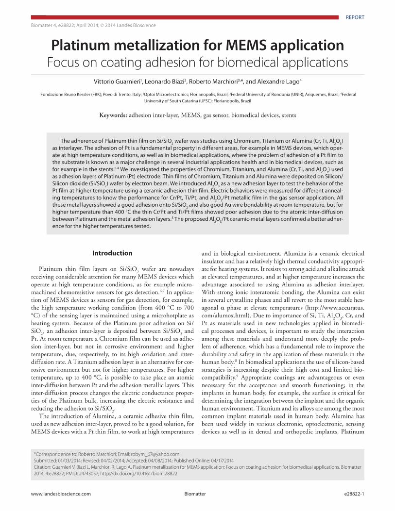
REPORT www.landesbioscience.com Biomatter e28822-1 Biomatter 4, e28822; April 2014; © 2014 Landes Bioscience REPORT Introduction Platinum thin film layers on Si/SiO 2 wafer are nowadays receiving considerable attention for many MEMS devices which operate at high temperature conditions, as for example micro- machined chemoresistive sensors for gas detection. 6,7 In applica- tion of MEMS devices as sensors for gas detection, for example, the high temperature working condition (from 400 °C to 700 °C) of the sensing layer is maintained using a microhotplate as heating system. Because of the Platinum poor adhesion on Si/ SiO 2 , an adhesion inter-layer is deposited between Si/SiO 2 and Pt. At room temperature a Chromium film can be used as adhe- sion inter-layer, but not in corrosive environment and higher temperature, due, respectively, to its high oxidation and inter- diffusion rate. A Titanium adhesion layer is an alternative for cor- rosive environment but not for higher temperatures. For higher temperature, up to 400 °C, is possible to take place an atomic inter-diffusion between Pt and the adhesion metallic layers. This inter-diffusion process changes the electric conductance proper- ties of the Platinum bulk, increasing the electric resistance and reducing the adhesion to Si/SiO 2 . The introduction of Alumina, a ceramic adhesive thin film, used as new adhesion inter-layer, proved to be a good solution, for MEMS devices with a Pt thin film, to work at high temperatures and in biological environment. Alumina is a ceramic electrical insulator and has a relatively high thermal conductivity appropri- ate for heating systems. It resists to strong acid and alkaline attack at elevated temperatures, and at higher temperature increases the advantage associated to using Alumina as adhesion interlayer. With strong ionic interatomic bonding, the Alumina can exist in several crystalline phases and all revert to the most stable hex- agonal α phase at elevate temperatures (http://www.accuratus. com/alumox.html). Due to importance of Si, Ti, Al 2 O 3 , Cr, and Pt as materials used in new technologies applied in biomedi- cal processes and devices, is important to study the interaction among these materials and understand more deeply the prob- lem of adherence, which has a fundamental role to improve the durability and safety in the application of these materials in the human body. 8 In biomedical applications the use of silicon-based strategies is increasing despite their high cost and limited bio- compatibility. 9 Appropriate coatings are advantageous or even necessary for the acceptance and smooth functioning; in the implants in human body, for example, the surface is critical for determining the integration between the implant and the organic human environment. Titanium and its alloys are among the most common implant materials used in human body. Alumina has been used widely in various electronic, optoelectronic, sensing devices as well as in dental and orthopedic implants. Platinum *Correspondence to: Roberto Marchiori; Email: [email protected] Submitted: 01/03/2014; Revised: 04/02/2014; Accepted: 04/08/2014; Published Online: 04/17/2014 Citation: Guarnieri V, Biazi L, Marchiori R, Lago A. Platinum metallization for MEMS application: Focus on coating adhesion for biomedical applications. Biomatter 2014; 4:e28822; PMID: 24743057; http://dx.doi.org/10.4161/biom.28822 Platinum metallization for MEMS application Focus on coating adhesion for biomedical applications Vittorio Guarnieri 1 , Leonardo Biazi 2 , Roberto Marchiori 3, *, and Alexandre Lago 4 1 Fondazione Bruno Kessler (FBK); Povo di Trento, Italy; 2 Optoi Microelectronics; Florianopolis, Brazil; 3 Federal University of Rondonia (UNIR); Ariquemes, Brazil; 4 Federal University of South Catarina (UFSC); Florianopolis, Brazil Keywords: adhesion inter-layer, MEMS, gas sensor, biomedical devices, stents The adherence of Platinum thin film on Si/SiO 2 wafer was studies using Chromium, Titanium or Alumina (Cr, Ti, Al 2 O 3 ) as interlayer. The adhesion of Pt is a fundamental property in different areas, for example in MEMS devices, which oper- ate at high temperature conditions, as well as in biomedical applications, where the problem of adhesion of a Pt film to the substrate is known as a major challenge in several industrial applications health and in biomedical devices, such as for example in the stents. 1-4 We investigated the properties of Chromium, Titanium, and Alumina (Cr, Ti, and Al 2 O 3 ) used as adhesion layers of Platinum (Pt) electrode. Thin films of Chromium, Titanium and Alumina were deposited on Silicon/ Silicon dioxide (Si/SiO 2 ) wafer by electron beam. We introduced Al 2 O 3 as a new adhesion layer to test the behavior of the Pt film at higher temperature using a ceramic adhesion thin film. Electric behaviors were measured for different anneal- ing temperatures to know the performance for Cr/Pt, Ti/Pt, and Al 2 O 3 /Pt metallic film in the gas sensor application. All these metal layers showed a good adhesion onto Si/SiO 2 and also good Au wire bondability at room temperature, but for higher temperature than 400 °C the thin Cr/Pt and Ti/Pt films showed poor adhesion due to the atomic inter-diffusion between Platinum and the metal adhesion layers. 5 The proposed Al 2 O 3 /Pt ceramic-metal layers confirmed a better adher- ence for the higher temperatures tested.
-
Upload
hoangthien -
Category
Documents
-
view
213 -
download
0
Transcript of Platinum metallization for MEMS application · 1Fondazione Bruno Kessler (FBK); povo di trento,...
RepoRt
www.landesbioscience.com Biomatter e28822-1
Biomatter 4, e28822; April 2014; © 2014 Landes Bioscience
RepoRt
Introduction
Platinum thin film layers on Si/SiO2 wafer are nowadays
receiving considerable attention for many MEMS devices which operate at high temperature conditions, as for example micro-machined chemoresistive sensors for gas detection.6,7 In applica-tion of MEMS devices as sensors for gas detection, for example, the high temperature working condition (from 400 °C to 700 °C) of the sensing layer is maintained using a microhotplate as heating system. Because of the Platinum poor adhesion on Si/SiO
2, an adhesion inter-layer is deposited between Si/SiO
2 and
Pt. At room temperature a Chromium film can be used as adhe-sion inter-layer, but not in corrosive environment and higher temperature, due, respectively, to its high oxidation and inter-diffusion rate. A Titanium adhesion layer is an alternative for cor-rosive environment but not for higher temperatures. For higher temperature, up to 400 °C, is possible to take place an atomic inter-diffusion between Pt and the adhesion metallic layers. This inter-diffusion process changes the electric conductance proper-ties of the Platinum bulk, increasing the electric resistance and reducing the adhesion to Si/SiO
2.
The introduction of Alumina, a ceramic adhesive thin film, used as new adhesion inter-layer, proved to be a good solution, for MEMS devices with a Pt thin film, to work at high temperatures
and in biological environment. Alumina is a ceramic electrical insulator and has a relatively high thermal conductivity appropri-ate for heating systems. It resists to strong acid and alkaline attack at elevated temperatures, and at higher temperature increases the advantage associated to using Alumina as adhesion interlayer. With strong ionic interatomic bonding, the Alumina can exist in several crystalline phases and all revert to the most stable hex-agonal α phase at elevate temperatures (http://www.accuratus.com/alumox.html). Due to importance of Si, Ti, Al
2O
3, Cr, and
Pt as materials used in new technologies applied in biomedi-cal processes and devices, is important to study the interaction among these materials and understand more deeply the prob-lem of adherence, which has a fundamental role to improve the durability and safety in the application of these materials in the human body.8 In biomedical applications the use of silicon-based strategies is increasing despite their high cost and limited bio-compatibility.9 Appropriate coatings are advantageous or even necessary for the acceptance and smooth functioning; in the implants in human body, for example, the surface is critical for determining the integration between the implant and the organic human environment. Titanium and its alloys are among the most common implant materials used in human body. Alumina has been used widely in various electronic, optoelectronic, sensing devices as well as in dental and orthopedic implants. Platinum
*Correspondence to: Roberto Marchiori; Email: [email protected]: 01/03/2014; Revised: 04/02/2014; Accepted: 04/08/2014; Published Online: 04/17/2014Citation: Guarnieri V, Biazi L, Marchiori R, Lago A. Platinum metallization for MEMS application: Focus on coating adhesion for biomedical applications. Biomatter 2014; 4:e28822; PMID: 24743057; http://dx.doi.org/10.4161/biom.28822
Platinum metallization for MEMS applicationFocus on coating adhesion for biomedical applications
Vittorio Guarnieri1, Leonardo Biazi2, Roberto Marchiori3,*, and Alexandre Lago4
1Fondazione Bruno Kessler (FBK); povo di trento, Italy; 2optoi Microelectronics; Florianopolis, Brazil; 3Federal University of Rondonia (UNIR); Ariquemes, Brazil; 4Federal University of South Catarina (UFSC); Florianopolis, Brazil
Keywords: adhesion inter-layer, MEMS, gas sensor, biomedical devices, stents
the adherence of platinum thin film on Si/Sio2 wafer was studies using Chromium, titanium or Alumina (Cr, ti, Al2o3) as interlayer. the adhesion of pt is a fundamental property in different areas, for example in MeMS devices, which oper-ate at high temperature conditions, as well as in biomedical applications, where the problem of adhesion of a pt film to the substrate is known as a major challenge in several industrial applications health and in biomedical devices, such as for example in the stents.1-4 We investigated the properties of Chromium, titanium, and Alumina (Cr, ti, and Al2o3) used as adhesion layers of platinum (pt) electrode. thin films of Chromium, titanium and Alumina were deposited on Silicon/Silicon dioxide (Si/Sio2) wafer by electron beam. We introduced Al2o3 as a new adhesion layer to test the behavior of the pt film at higher temperature using a ceramic adhesion thin film. electric behaviors were measured for different anneal-ing temperatures to know the performance for Cr/pt, ti/pt, and Al2o3/pt metallic film in the gas sensor application. All these metal layers showed a good adhesion onto Si/Sio2 and also good Au wire bondability at room temperature, but for higher temperature than 400 °C the thin Cr/pt and ti/pt films showed poor adhesion due to the atomic inter-diffusion between platinum and the metal adhesion layers.5 the proposed Al2o3/pt ceramic-metal layers confirmed a better adher-ence for the higher temperatures tested.

e28822-2 Biomatter Volume 4
is used to make essential components for a range of medical devices, including pacemakers, implantable defibrillators, cath-eters, stents, and neuromodulation devices. The properties of platinum which make it suitable for medical device applications include its biocompatibility, inertness within the body, durabil-ity, electrical conductivity, and radiopacity. More recently, its unique properties have been exploited in catheters that incorpo-rate platinum components for the treatment of brain aneurysms. Afterwards, a small tubular device, the stent, is usually inserted in catheters in order to keep the newly-cleared artery open. The successful development and implementation of these strategies in health care are intrinsically expected to improve the clinical performances of medical devices, thus enhancing the life quality of patients, significantly lowering medical treatment costs and providing new technological solutions.9
Results
MEMS fabrication processDevices for testing structure produced using silicon-based
technology have been designed using L-Edit Tanner tools. The chip has been fabricated using microtechnology. The starting material for electrodes fabrication was (100) 4-inch, p-type silicon wafer, CZ double polished. The structure has been realized onto the substrate by a 500-nm-thick layer of silicon oxide growth by thermal wet oxidation followed by a 150-nm-thick stoichiometric Si
3N
4 film deposited by LPCVD (Low Pressure Chemical Vapor
Deposition). A further insulating multilayer (500-nm undoped TEOS oxide) was deposited. A Cr/Pt, Ti/Pt or Al
2O
3/Pt differ-
ent layers have been deposited by evaporation on the front trough a negative photoresist and etched with a lift off technique. After initial period, the stability of platinum heater fabricated in this way was satisfactory at temperature up to 450 °C (about 0.01% drift per day) (Fig. 1). The TCR value measured at T
0 = 20 °C
was 2800 ppm/°C.Sheet resistance measurementsFigure 2 shows the sheets electrical resistance testing machine
obtained by a four point prober. The electrical resistance, shown in Figure 3, was repeated in three different positions on the sur-face of the samples, to verify the eventual fluctuation of resistance.
The standard deviation showed a very little fluctuation depend-ing on position on the surface. The electrical resistance decreased with the increasing of annealing temperature for all samples. It’s also possible to note that until 600 °C the samples in Nitrogen flow processing conditions presented a slightly lower resistance. The Alumina samples showed a behavior like Titanium samples, with lower resistance than Chromium.
Temperature coefficient of resistance (TCR)The TCR coefficient describes the electrical resistance behav-
ior vs. annealing temperature and it is quoted in terms of parts per million per degrees Centigrade.
The term “ppm/°C” is not specific to resistors, but applies to almost every single electronic component ever produced and is a measure of how much the component’s stability will drift in response to a change in temperature. That is usually measured in terms of “parts per million per degrees centigrade” (ppm/°C). The meaning of “parts” is the unit used in the measure of that component; in this case it is Ohms.
It is important to evaluate a curve of the resistance vs tem-perature (R[T]) of the sensors in laboratory conditions to obtain their thermal behavior. For this purpose we designed a dedicated oven. The oven’s chamber has a socket for the sensor and it is electrically connected through isolated wires and it is possible
Figure 1. MeMS fabrication process. (A) LoR 5A (Microchem photoresist for lift off) and positive photoresist deposited by lithography on Si/Sio2 sub-strate; (B) photoresist exposure to UV light; (C) Develop resist and LoR. LoR develops isotropically, creating a bi-layer reentrant sidewall profile; (D) Deposited films. the re-entrant profile ensures discontinuous film deposition; (E) Lift-off bi-layer resist stack, leaving only the desired film.
Figure 2. Sheet resistance measured by digital four probe station (Napson RG-8).

www.landesbioscience.com Biomatter e28822-3
Figure 3. the sheets electrical resistance.
Figure 4. tCR behavior vs. annealing temperature for samples with Alumina, titanium or Chromium as adhesion layer, under oxygen or nitrogen gas flow.

e28822-4 Biomatter Volume 4
to measure three different resistances at the same time, control-ling the heating rate and recording every data in the computer. Elaborating these data are possible to know the equation of the curve and the Temperature Coefficient Resistance (TCR) of the sensor.
Figure 4 shows the TCR values of the samples depending from annealing temperatures and from gas flow. In this work was realized a preliminary study of the TCR behavior of the samples, to indicate how the resistance is changing with growing of tem-perature in different atmosphere conditions. So the measure was realized one single time for every condition of temperature and gas. In all samples the TCR coefficient increased with increasing of annealing temperature; this behavior was more efficient using an oxygen gas flow than a nitrogen gas flow. The Titanium and Alumina samples had a similar behavior.
Image analysis: SEM characterizationThrough SEM images, showed in the Figure 5, is possible to
verify the surface aspect after annealing for Alumina samples. Until 500 °C, the surfaces for all samples haven’t alterations, for 600 °C and 700 °C in the corners of the Platinum surfaces are present similar alterations. For samples with Oxygen flow the
surfaces present black points. Although these modifications, the adhesion of Al
2O
3/Pt film and the electrical properties continued
stable.Image analysis: FEG characterizationThrough FEG analysis, showed in the Figure 6, is possible to
verify the surface aspect and to compare the presence of defects on different samples, depending from the annealing temperature and from the adhesion interlayer.
The picture of FEG characterization of the sample with Cr adhesion interlayer show the presence of defects in the surface, that seem like holes, when the annealing was carried out at 700 °C (Fig. 7D). That was probably due to tension between the surface of Si and the deposited film of Cr, more effective in the higher temperature.
The FEG image of sample with Al2O
3 interlayer, annealed
at 700 °C, showed the presence of very little defect at the sur-face, when compared with the defect of samples with Cr inter-layer annealed at the same temperature; the presence of that little defects didn’t affect the electrical properties of that samples.
The FEG images of surface of the samples with Ti inter-layer didn’t show any difference depending from annealing
Figure 5. SeM images of Al2o3/pt film indicate a modification of the surface due to annealing at 500 °C. (A) and (B) Samples surface after a 400 °C anneal-ing; (C) and (E) 700 °C annealing with oxygen flow, with appearing of black points; (D) and (F) 700 °C annealing with Nitrogen flow.
Table 1. Summary of the annealing treatment.
Layer Thickness (nm)Heating rate
˚C/minFlux (sccm)
Lithography Temperature range (˚C)O2 N2
Al2o3/pt 5/150 10 32 32 positive 300 to 700
Cr/pt 5/150 10 32 32 positive 300 to 700
ti/pt 10/150 10 32 32 positive 300 to 700

www.landesbioscience.com Biomatter e28822-5
temperature, evidencing that the surface was very stable in this range of temperature.
Discussion
We can see, through Figure 1 and Figure 2, the lower yield for Chromium samples vs. Titanium and Alumina. The Chromium is a material with high inter-diffusion rate on Platinum, conse-quently, the adhesion force in these samples has a several reduc-tion when annealing temperature increases. Another problem for the high inter-diffusion rate is the difficult to reach a stable
state; in others words, the electrical properties for Chromium samples change every time that we subject the sample to the same annealing temperature. The Titanium samples has a good electri-cal behavior for the annealing process, however the adhesion of the film can be severally reduced with the growing of annealing temperature. In all the samples the adherence of the Pt film on the surface, reached through the presence of an interlayer of Cr, Ti or Alumina, was influenced on the gas atmosphere used to anneal the samples and in higher temperatures an oxygen flow reduced the problem of a lost in adherence of the samples sur-face. In the evaporation of Alumina, the electron-beam evapora-tor produces a non-stoichiometric film due to oxygen deficiency.1
Figure 6. FeG images, with magnification of 10.000 X. the pictures show the surface of samples with Al2o3, Cr, and ti adhesion layer, annealed to 300 °C and 700 °C in a oxygen flow. (A) and (B): Al2o3interlayer, with annealing of 300 °C and 700 °C. (C) and (D): Cr interlayer, annealed at 300 °C and 700 °C. (E) and (F): ti interlayer, where annealing was performed at 300 °C and 700 °C.

e28822-6 Biomatter Volume 4
Increasing the temperature under oxygen gas flow, we enhance the oxidation improving the stability of the oxide film through the decrease of stoichiometric imbalance. To have very complete results is necessary to carry out a chemical surface analysis to characterize the different phases of the films depending from annealing temperatures.
Experimental
Sample preparationAll thin films of Chromium (Cr, 5 nm thickness), Titanium
(Ti, 5 nm thickness), Alumina (Al2O3, 10 nm thickness) were
deposited by electron beam evaporator (Fig. 8. Ulvac EBX – 16C e – gun Ferrotec EV S – 6) as different adhesion layers on Si/SiO
2 substrate, with Platinum (Pt, 150 nm thickness) as metal
resistor film.Annealing treatmentAfter deposition, the samples were annealed at different tem-
peratures from 300 °C to 700 °C, by step of 100 °C. The anneal-ing set point was obtained increasing the temperature at a rate of 10 °C per minute (Fig. 9). All samples were annealed for 1 h. For the annealing treatment we used two different gases, Oxygen and Nitrogen, with a gas flow of 32 sccm (Table 1).
Characterization
Figure 7. Set up system to determine the tCR value of the pt metallization
Figure 8. Representation of the electron beam evaporator. High vacuum condition, about 10–7 torr.

www.landesbioscience.com Biomatter e28822-7
The electrical resistance, before and after annealing, was mea-sured by a sheet resistance test using a ST3–1 digital four point probe (Napson RG-8) at 20 °C. The Temperature Coefficient of Resistance (TCR) was calculated by measuring the change in the electrical resistance per degree of temperature, controlling the temperature using a special furnace. The TCR values were deter-mined through the equation:
R(T) = Rref × [1 + á(T - Tref)]where R(T) is the conductor resistance at temperature “T,” R
ref
is the conductor resistance at reference temperature Tref
= 0 °C and α is the thermal coefficient of resistance, specified for any conductor material. T and T
ref are, respectively, the conductor
temperature and the reference temperature in degrees Celsius.Roughness and thickness analysis were made by optical pro-
filometry scanning (KLA – Tencor P – 15 stylus profilometer). The films adherence and the atomic interdiffusion between sub-strate and interlayer and between interlayer and film were studied through Optical Microscopy (Leitz Ergolux), Scanning Electron Microscopy (JOEL JSM – 6100), and through FEG-SEM
Field Emission Gun Scanning Microscopy (JEOL, SEM-FEG JSM-6701F).
Conclusions
The application of Alumina, produced by electron bombard-ment, as a new adhesion layer material for gas and biological sensors and in biomedical applications, appears as an excellent alternative to improve the adherence of the platinum surface on the Si/SiO
2 substrate. Alumina is electrically insulating, optically
transparent, chemically stable, bio-inert and biocompatible mate-rial, with a good adhesion on Si/SiO
2 in higher temperatures and
with remarkable electrical properties when used as an adhesion layer film between Si/SiO
2 and Platinum.
Disclosure of Potential Conflicts of Interest
No potential conflicts of interest were disclosed.
Figure 9. Curve and photo of an annealing process in the minibrute furnace by Nitrogen gas flow.
References1. Lewis F., Turgeon S., Chevallier P., Pireaux J-J., Tatoulian
M., Mantovani D. On the growth of f luorocarbon thin films deposited on plasma etched 316L stainless steel. Plasma Processes and Polymers 2009; 7: 309-317; http://dx.doi.org/10.1002/ppap.200900107
2. Nelea V, Holvoet S, Turgeon S, Mantovani D. Deposition of f luorocarbon thin films on outer and inner surfaces of stainless steel mini-tubes by pulsed plasma polymerization for stents. J Phys D: Appl Phys 2009; 42: 225208; http://dx.doi.org/10.1088/0022-3727/42/22/225208
3. Lewis F, Mantovani D. Methods to Investigate the Adhesion of Soft Nano-Coatings on Metal Substrates—Application to Polymer-Coated Stents. Macromol Mater Eng 2009; 249:11-9; http://dx.doi.org/10.1002/mame.200800229
4. Lewis F, Mantovani D. Coated Stents: How to inves-tigate the adhesion of the coating? A comparative review. Macromol Mater Eng 2009; 294:11-9; http://dx.doi.org/10.1002/mame.200800229
5. Vincenzi D, Butturi MA, Guidi V, Carotta MC, Martinelli G, Guarnieri V, Brida S, Margesin B, Giacomozzi F, Zen M, et al. Development of a low-power thick-film gas sensor deposited by screen-printing technique onto a micromachined hotplate. Sens Actuators B Chem 2001; 77:95-9; http://dx.doi.org/10.1016/S0925-4005(01)00679-7
6. Adami A, Lorenzelli L, Guarnieri V, Francioso L, Forleo A, Agnusdei G, Taurino AM, Zen M, Siciliano P. A WO3-based gas sensor array with linear tem-perature gradient for wine quality monitoring. Sens Actuators B Chem 2006; 117:115-22; http://dx.doi.org/10.1016/j.snb.2005.11.006
7. Mailly F, Giani A, Bonnot R, Temple-Boyer P, Pascal-Delannoy F, Foucaran A, Boyer A. Anemometer with hot platinum thin film. Sens Actuators A Phys 2001; 94:32-8; http://dx.doi.org/10.1016/S0924-4247(01)00668-9
8. Cowley A, Woodward B. A Healthy Future: Platinum in Medical Applications. Platin Met Rev 2011; 55:98-107; http://dx.doi.org/10.1595/147106711X566816
9. Nguyen, NT. Fabrication Issues of Biomedical Micro Devices. BioMEMS and Biomedical Nanotechnology 2007; 2007:93–115