Platform Based Design: Report from the...
22
Platform Based Design: Report from the Front Sagheer Ahmad Kambiz Khalilian Daniel Martin EDP-2002 Apr 22, 2002
Transcript of Platform Based Design: Report from the...

Platform Based Design:
Report from the Front
Sagheer Ahmad
Kambiz Khalilian
Daniel Martin
EDP-2002Apr 22, 2002
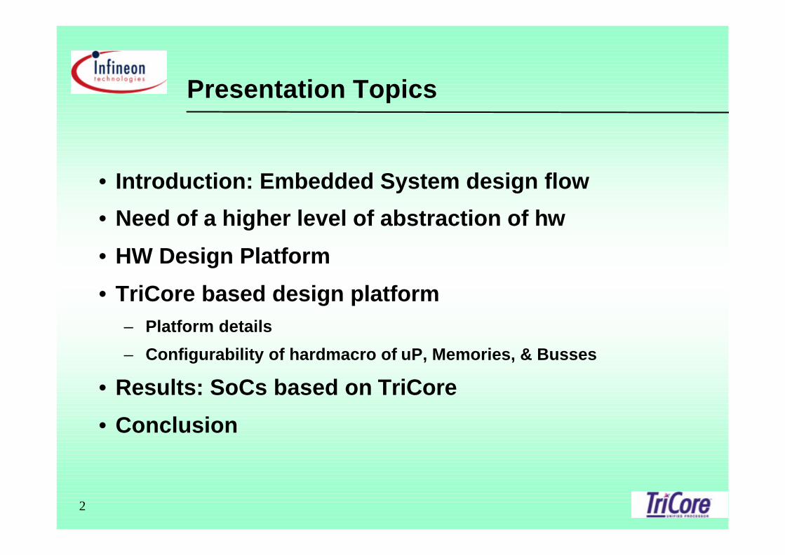
Presentation Topics
• Introduction: Embedded System design flow
• Need of a higher level of abstraction of hw
• HW Design Platform
• TriCore based design platform– Platform details
– Configurability of hardmacro of uP, Memories, & Busses
• Results: SoCs based on TriCore
• Conclusion
2

Embedded System (or HW/SW co-)Design Flow - A Simple view
System Behavior
Partitioning
Partitioned Spec.
HW developmentSW development
Standard components Board Level Prototype
Physical Prototype
Partition into blocks&Un-optimized HW
Logic Synthesis
Back End(FP & PnR)
Co-simulation
Form
al (&
Fun
c)V
erifi
catio
n
Fun
c V
erif.
Perf. insufficient
3

HW components of an Embedded Sys.
• Embedded Systems are implemented as mixed sw-hwsystems. SW is, generally, used for features and flexibility,and HW is used for performance {e.g. Cameras, cellphones,industrial controllers, etc.}.
• Compute Engine: Microcontroller, uP/uC (RISC), DSP• Program and Data Cache/Memories (Varying Size)• One or more Buss-Interconnects• Application specific HW• DMA, Interrupt support• General Purpose Peripherals
4

HW components of an Embedded Sys.
• General Purpose Peripherals (GPP):
–ASC: Async./Sync. Serial Interface–SSC: High Speed Synch. Serial Control– UART: Universal Asynchronous Rx/Tx–IIC: Inter-Integrated Circuit, Serial Bus–RTC: Real Time Clock–STM: System Timer–GPTU: 3x 32-bit General Purpose Timers–GPIO: Up to 64 General Purpose I/O–WDT: Watch Dog Timer– …. etc.
5
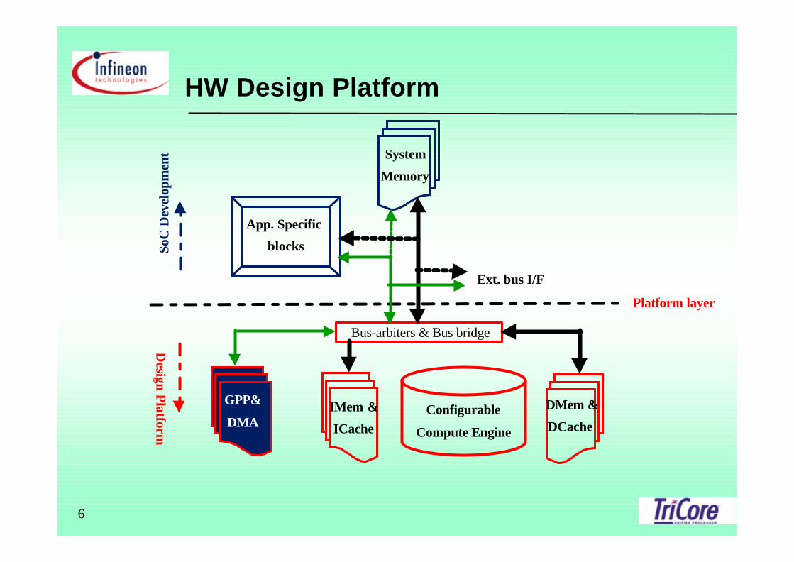
HW Design Platform
SoC
Dev
elop
men
t System
Memory
App. Specific
blocks
Platform layer
Configurable
Compute Engine
IMem &
ICache
DMem &
DCache
GPP&
DMA
Design Platform
Bus-arbiters & Bus bridge
Ext. bus I/F
6

App Specific
(IP)
Value-added
Blocks
HW Design Platform (cont..)
From the platform (GUI or HDL):
•RISC @200Mhz worst,250MIPs
•DSP @200 Mhz worst, 300MMs
•IMem (32KB), Icache(16KB)
•DMem(32 KB), Dcache(16KB)
•GPPs (ASC,RTC,I2C,STM,GPT,GIO)
•DMA, & Interrupt service
PeripheralsuP/DSP
Cache/Mem
Interconnects
Develop HDL:
• Application specific blocks
• System Memory (compiler generated)
• Top level interconnect signal hook-up.
7

Platform Deliverables
•RTL with synthesis scripts (For soft-macro)
•Timing shell, Timing Analysis scripts, Backend views (ForHardmacro)
•Bus Function models for bus interconnects
•High level compute-engine model
– ISS and/or Cycle-Accurate
•High level models for GPPs
•Verification environment/methodology
•Basic Software
– Boot code, basic handler, test-programs*, Tests vectors
– RTOS
8
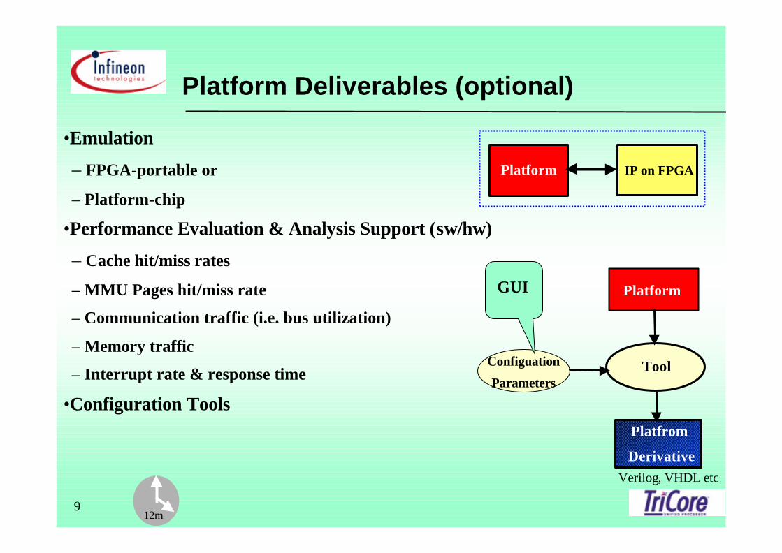
Platform Deliverables (optional)
•Emulation
– FPGA-portable or
– Platform-chip
•Performance Evaluation & Analysis Support (sw/hw)
– Cache hit/miss rates
– MMU Pages hit/miss rate
– Communication traffic (i.e. bus utilization)
– Memory traffic
– Interrupt rate & response time
•Configuration Tools
Platform IP on FPGA
Verilog, VHDL etc
Tool
Platform
Platfrom
Derivative
Configuation
Parameters
GUI
12m9

Embedded System (or HW/SW co-)Design Flow with Design Platform
System Behavior
Partitioning
Partitioned Spec.
HW developmentSW development
Standard components Board Level Prototype
Physical Prototype
Logic Synthesis
Back End(FP & PnR)
Co-simulation
Un-optimized HW
Form
al (&
Fun
c)V
erifi
catio
n
Fun
c V
erif.
IP HW & Integ
Form
al (&
Fun
c)V
erifi
catio
n
Fun
c V
erif.
Perf. insufficient
11

TriCore - TC1 Architecture Overview
• 32-bit Unified RISC+DSP
• Load/Store Architecture
• HW controlled context saving
• Fast context switch (shadow registers)
• Fast interrupt response (~6 clocks)
• Superscalar: Three pipelines
• Zero Overhead loop
• 16-bit / 32-bit Instruction Format
• Single-cycle dual MAC
– 32x32, 16x32, Dual 16x16
• On-Chip debug support
• MMU, COP• TC1 (300Mhz, typ, 0.18u), TC2 (600Mhz,typ, 0.13u)
Data Memory Interface
Program Memory Interface
DataRegister
s
AddressRegisters
InstructionFetch
Load/Store Unit
ArithmeticALU
IntegerALU
BitProcessing
Unit
Pip
elin
e C
ontr
ol
MAC
Coprocessor
BranchPredict Unit
Data &InstructionAlignment
MemoryProtection
MM
U
TC1 CPU
12

TriCore1 SOC Platform - TCSOC
Loc
al M
emor
y B
us (L
MB
)
SSC x 2
ASC x 2Fle
xibl
e P
erip
hera
l Int
erco
nnec
t B
us
Program Memory
TriCore1 CPU
Data Memory
Data Memory Interface
Program Memory Interface
DataRegister
s
AddressRegisters
InstructionFetch
Load/Store Unit
ArithmeticALU
IntegerALU
BitProcessing
Unit
Pip
elin
e C
ontr
ol
MAC
Coprocessor
BranchPredict Unit
Data &InstructionAlignment
MemoryProtection
MM
U
Debug/Emulation
Interrupt Unit
CPS
FPI I/F
BusBridge
PCP
GPTU
RTC
SCU
BCU
TCU
IIC
EBU
GPIO
STM
13

• TriCore1 Microprocessor System (MPS)• Configurable Program & Data Cache/Memory I/F• optional MMU and FPU.
• PCP : 32-bit Peripheral Control Processor Processor• 64 (low latency) & 32 bit busses• Set of System- and General Purpose Peripherals:
– ASC: Async./Sync. Serial Interface– IIC: Two channel I2C Serial Bus– RTC: Real Time Clock– SSC: High Speed Synch. Serial Control (SPI-compatible)– STM: System Timer– GPTU: 3x 32-bit General Purpose Timers– GPIO: Customizable General Purpose I/O– EBU: External Bus Interface for Off-Chip Memory– Test Control Unit (OCDS & JTAG I/F)– System Control Unit (Reset Control, Power Management,Watch Dog Timer)
TCSOC: Compute Engine,TriCore1
14
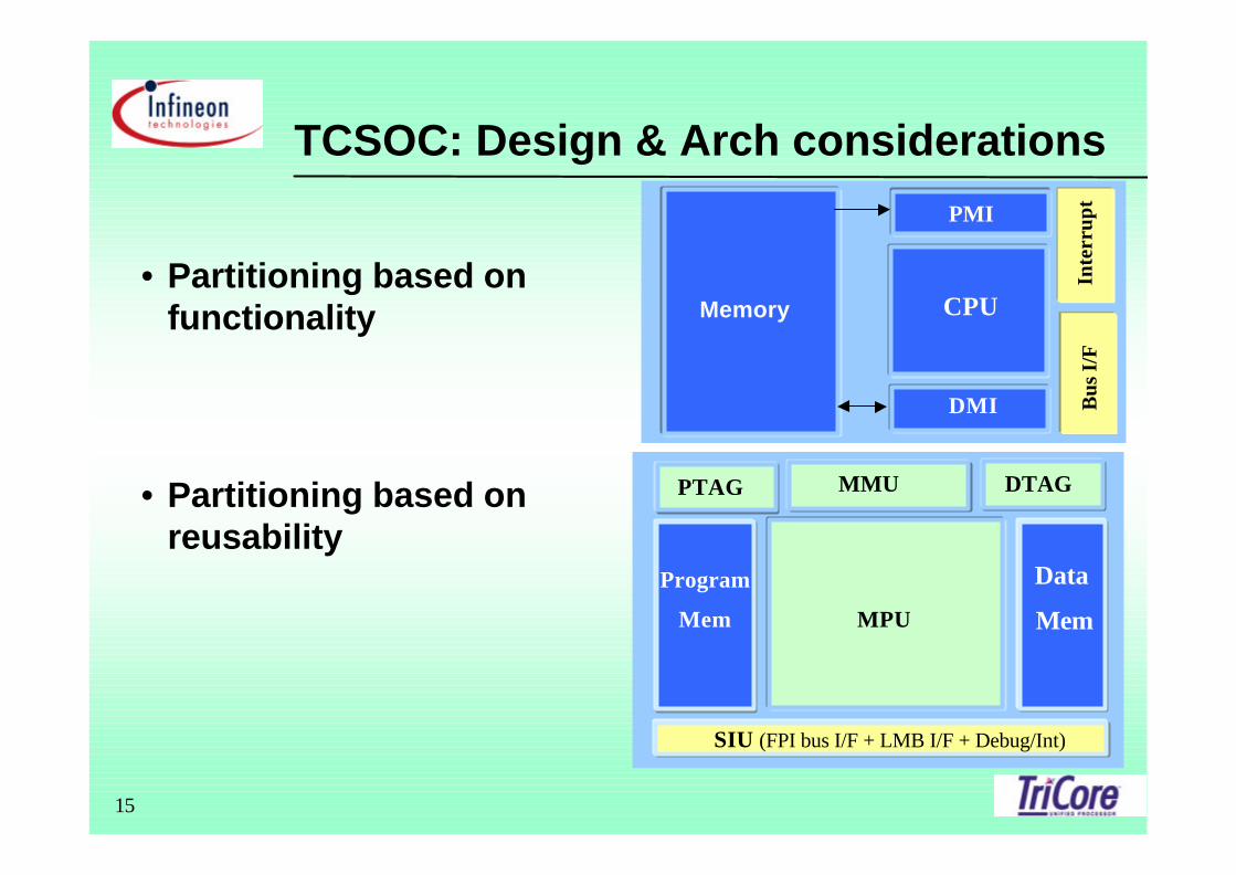
TCSOC: Design & Arch considerations
• Partitioning based onfunctionality
• Partitioning based onreusability
Memory
DMI
PMI
CPU
Bus
I/F
Inte
rrup
t
Program
Mem MPU
SIU (FPI bus I/F + LMB I/F + Debug/Int)
Data
Mem
MMUPTAG DTAG
Program
Mem
15
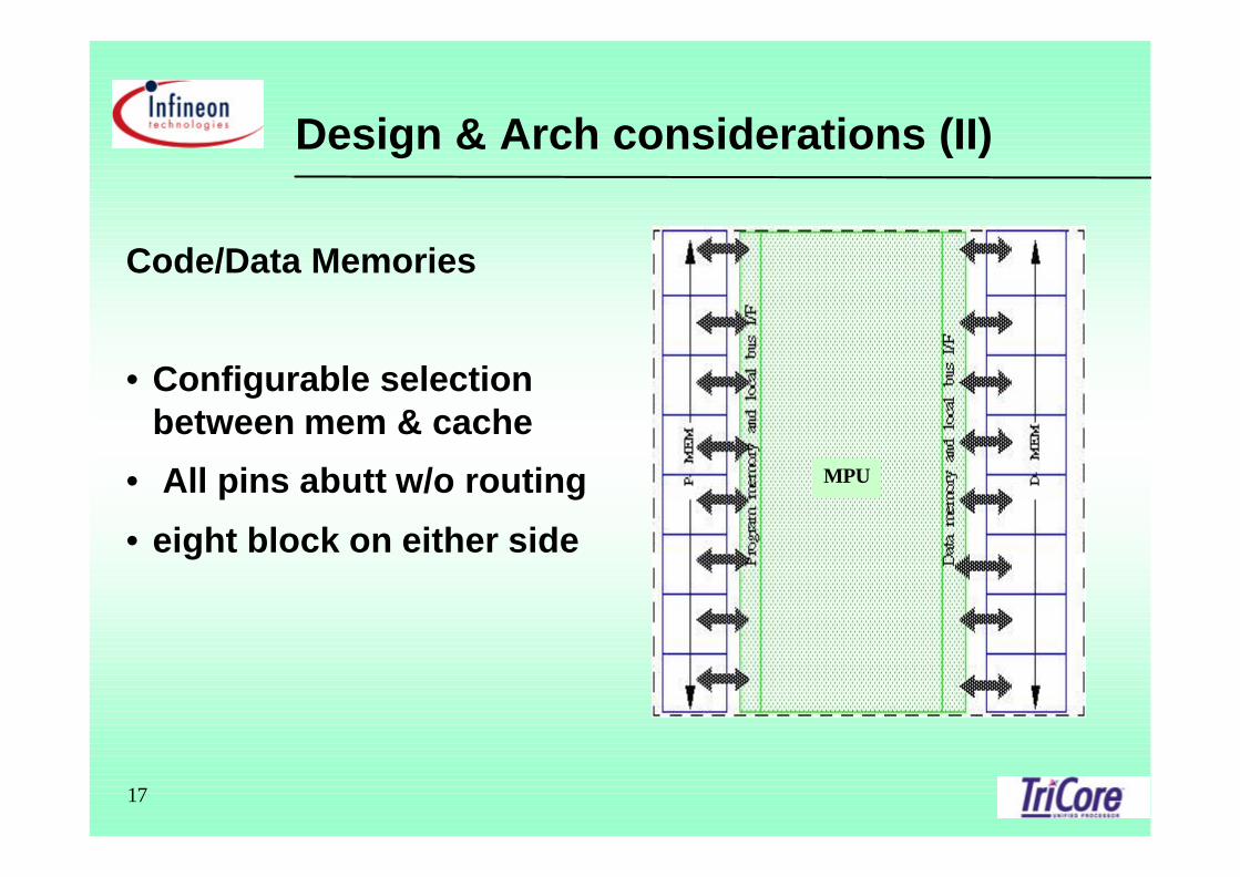
Design & Arch considerations (II)
Code/Data Memories
• Configurable selectionbetween mem & cache
• All pins abutt w/o routing
• eight block on either side
MPU
17

• TC1 MPS : TriCore1 Microprocessor System• Configurable Program & Data Cache/Memory I/F• optional MMU and FPU.
• PCP : 32-bit Peripheral Control Processor• 64 (low latency) LBM, & 32 bit FPI• Set of System- and General Purpose Peripherals:
– ASC: Async./Sync. Serial Interface– IIC: Two channel I2C Serial Bus– RTC: Real Time Clock– SSC: High Speed Synch. Serial Control (SPI-compatible)– STM: System Timer– GPTU: 3x 32-bit General Purpose Timers– GPIO: Customizable General Purpose I/O– EBU: External Bus Interface for Off-Chip Memory– Test Control Unit (OCDS & JTAG I/F)– System Control Unit (Reset Control, Power Management,Watch Dog Timer)
TCSOC: Bus Interconnects (LMB & FPI)
22

TCSOC: Bus Interconnects (cont..)
• 64 bit on-chip & off-chipbus I/F
• 32 bit on-chip & off-chipbus I/F
• Large no. of peripherals?
• System bus & cpu freqratio 1:1, 1:2, …, 1:n– Signal configurable
MPU
SIULocal bus
64 bit Bus bridge
32 bit system bus
per0 per1……...
64 bit
Mem Mem
perN
24
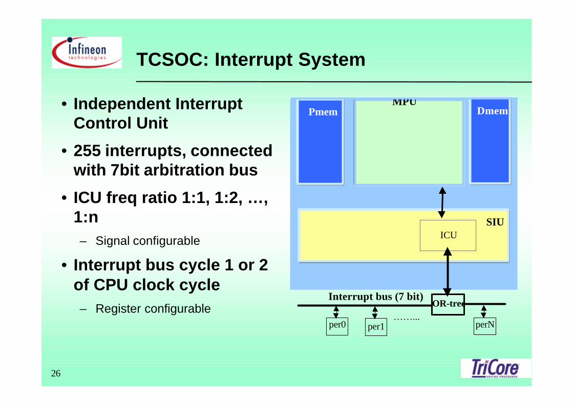
TCSOC: Interrupt System
• Independent InterruptControl Unit
• 255 interrupts, connectedwith 7bit arbitration bus
• ICU freq ratio 1:1, 1:2, …,1:n– Signal configurable
• Interrupt bus cycle 1 or 2of CPU clock cycle– Register configurable
MPU
SIUICU
Interrupt bus (7 bit)
per0 per1……...
perN
Pmem Dmem
OR-tree
26

Telematics Controller – TC1920
29

Triple-Mode Baseband IC
MPU
30

Conclusion
Design Platform:
• High-performance configurable RISC/DSP
• Bus interconnects (at least one low latency)
• General Purpose Peripherals
• PCP, and Interrupt system
By Using Design Platform:
• Quick development of derivative designs (i.e. SoC).
• Designer concentrates on system design rather thancomponents
• Designer uses a proven design methodology
31

EDP-2002
Never Stop Thinking
Sagheer Ahmad
Kambiz Khalilian
Daniel Martin
http://www.infineon.com/tricore/