Plastic Solar Cells** - University of Cagliari · Plastic Solar Cells** By Christoph J. Brabec, N....
12
Plastic Solar Cells** By Christoph J. Brabec, N. Serdar Sariciftci,* and Jan C. Hummelen 1. Prologue It is intriguing to think of photovoltaic (PV) elements based on thin plastic films. The flexibility offered through the chemical tai- loring of desired properties, as well as the cheap technology already well developed for all kinds of plastic thin film applica- tions would make such an approach a sure hit. The mechanical flexibility of plastic materials is welcome for all PV applications onto curved surfaces for architectural integration. By casting semi-transparent plastic PV thin films between insulating win- dow glass, large unused areas (the windows) can be employed for power generation in addition to the limited roof areas of crowded cities. Even the color of such PV elements can be varied by sacrificing some parts of the visible solar spectrum. An encouraging breakthrough in realizing higher efficiencies has been achieved by mixing electron–donor-type polymers with suitable electron acceptors. The photophysics of conju- gated polymer/fullerene solid composites has been particularly well investigated over the last eight years. An understanding of the photophysics in detail has allowed the realization of proto- type PV devices with solar power conversion efficiencies of around 3 %, and this has in turn triggered enhanced emphasis from several groups worldwide, pursuing this research with in- creasing support from industry as well as public funding agencies. On the other hand there is a common problem for all the applications of conjugated polymers: stability. Even though the expectation on the lifetimes of electronic devices is shrinking due to very short life/fashion cycles of such applications and even though industry may be interested in the cost of an item rather than in a very long durability of it, a shelf lifetime of several years as well as an operational lifetime of tens of thou- sands of hours are requested for all durable applications. Con- jugated polymers have to be protected from air and humidity to achieve such lifetimes. These protection methods are being developed for light emitting diodes (LEDs) as well as PV ele- ments. Their effectiveness is going to be crucial for the success of any applications using these materials. Recent reports from LED research indicate that the stability problem has been suf- ficiently overcome in order to enter into large scale applica- tions, which in turn is a good sign for plastic solar cells. It is the purpose of this review to give a state of the art report on plastic solar cells based on conjugated polymers as well as to give a basic introduction to the underlying photophysics. 2. Device Architectures 2.1. Single Layer Diodes The simplest and most widely used organic semiconductor device is a metal–insulator–metal (MIM) tunnel diode with metal electrodes of asymmetrical workfunction (Fig. 1). Under forward bias, holes from the high workfunction metal and electrons from the low workfunction metal are injected into a thin film of a sin- gle-component organic semiconductor. Because of the asymme- try of the workfunction of the cathode and the anode, forward bias currents for a single carrier type material are orders of mag- nitude larger than reverse bias currents at low voltages. The recti- fying diode characteristics can be accompanied by radiative – [*] Prof. N. S. Sariciftci,Dr. C. J. Brabec Linzer Institut für organische Solarzellen (LIOS) Physikalische Chemie, Johannes Kepler Universität Linz Altenbergerstr. 69, A-4040 Linz (Austria) E-mail: [email protected] Prof. J. C. Hummelen Organic and Molecular Inorganic Chemistry, University of Groningen Nijenborgh 4, NL-9747 AG Groningen (The Netherlands) [**] The authors gratefully acknowledge the co-workers at the University of Linz and at the University of Groningen. as well as our numerous interna- tional collaboration partners. Financial supports of both the Universities, European Commission (DGXII, JOULE III), Quantum Solar Energy Linz GesmbH (Austria), Christian Doppler Society, the Magistrat Linz, the Land Oberösterreich (ETP), Austrian Foundation for Scientific Research (FWF P-12680CHE) as well as Netherlands Agency for Energy and Envi- ronment (NOVEM) and EET (The Dutch R&D Programme on Energy, Environment and Technology) are gratefully acknowledged. Recent developments in conjugated-polymer-based photovoltaic elements are reviewed. The photophysics of such photoactive devices is based on the photo-induced charge transfer from donor-type semiconducting conjugated polymers to acceptor-type conjugated polymers or acceptor molecules such as Buckminsterfullerene, C 60 . This photo-induced charge transfer is reversible, ultrafast (within 100 fs) with a quantum efficiency approaching unity, and the charge-separated state is metastable (up to milliseconds at 80 K). Being similar to the first steps in natural photosynthesis, this photo-induced electron transfer leads to a number of potentially interesting applications, which include sensitization of the photoconductivity and photovoltaic phenomena. Examples of photovoltaic architectures are presented and their potential in terrestrial solar energy conversion discussed. Recent progress in the realization of improved photovoltaic elements with 3 % power conversion efficiency is reported. Adv. Funct. Mater. 2001, 11, No. 1, February Ó WILEY-VCH Verlag GmbH, D-69469 Weinheim,2001 1616-301X/01/0102-0015 $ 17.50+.50/0 15 FEATURE ARTICLE
Transcript of Plastic Solar Cells** - University of Cagliari · Plastic Solar Cells** By Christoph J. Brabec, N....

Plastic Solar Cells**
By Christoph J. Brabec, N. Serdar Sariciftci,* and Jan C. Hummelen
1. Prologue
It is intriguing to think of photovoltaic (PV) elements based onthin plastic films. The flexibility offered through the chemical tai-loring of desired properties, as well as the cheap technologyalready well developed for all kinds of plastic thin film applica-tions would make such an approach a sure hit. The mechanicalflexibility of plastic materials is welcome for all PV applicationsonto curved surfaces for architectural integration. By castingsemi-transparent plastic PV thin films between insulating win-dow glass, large unused areas (the windows) can be employed forpower generation in addition to the limited roof areas ofcrowded cities. Even the color of such PVelements can be variedby sacrificing some parts of the visible solar spectrum.
An encouraging breakthrough in realizing higher efficiencieshas been achieved by mixing electron±donor-type polymerswith suitable electron acceptors. The photophysics of conju-gated polymer/fullerene solid composites has been particularlywell investigated over the last eight years. An understanding ofthe photophysics in detail has allowed the realization of proto-type PV devices with solar power conversion efficiencies ofaround 3 %, and this has in turn triggered enhanced emphasis
from several groups worldwide, pursuing this research with in-creasing support from industry as well as public funding agencies.
On the other hand there is a common problem for all theapplications of conjugated polymers: stability. Even though theexpectation on the lifetimes of electronic devices is shrinkingdue to very short life/fashion cycles of such applications andeven though industry may be interested in the cost of an itemrather than in a very long durability of it, a shelf lifetime ofseveral years as well as an operational lifetime of tens of thou-sands of hours are requested for all durable applications. Con-jugated polymers have to be protected from air and humidityto achieve such lifetimes. These protection methods are beingdeveloped for light emitting diodes (LEDs) as well as PV ele-ments. Their effectiveness is going to be crucial for the successof any applications using these materials. Recent reports fromLED research indicate that the stability problem has been suf-ficiently overcome in order to enter into large scale applica-tions, which in turn is a good sign for plastic solar cells.
It is the purpose of this review to give a state of the art reporton plastic solar cells based on conjugated polymers as well asto give a basic introduction to the underlying photophysics.
2. Device Architectures
2.1. Single Layer Diodes
The simplest and most widely used organic semiconductordevice is a metal±insulator±metal (MIM) tunnel diode with metalelectrodes of asymmetrical workfunction (Fig. 1). Under forwardbias, holes from the high workfunction metal and electrons fromthe low workfunction metal are injected into a thin film of a sin-gle-component organic semiconductor. Because of the asymme-try of the workfunction of the cathode and the anode, forwardbias currents for a single carrier type material are orders of mag-nitude larger than reverse bias currents at low voltages. The recti-fying diode characteristics can be accompanied by radiative
±[*] Prof. N. S. Sariciftci, Dr. C. J. Brabec
Linzer Institut für organische Solarzellen (LIOS)Physikalische Chemie, Johannes Kepler Universität LinzAltenbergerstr. 69, A-4040 Linz (Austria)E-mail: [email protected]
Prof. J. C. HummelenOrganic and Molecular Inorganic Chemistry, University of GroningenNijenborgh 4, NL-9747 AG Groningen (The Netherlands)
[**] The authors gratefully acknowledge the co-workers at the University ofLinz and at the University of Groningen. as well as our numerous interna-tional collaboration partners. Financial supports of both the Universities,European Commission (DGXII, JOULE III), Quantum Solar Energy LinzGesmbH (Austria), Christian Doppler Society, the Magistrat Linz, theLand Oberösterreich (ETP), Austrian Foundation for Scientific Research(FWF P-12680CHE) as well as Netherlands Agency for Energy and Envi-ronment (NOVEM) and EET (The Dutch R&D Programme on Energy,Environment and Technology) are gratefully acknowledged.
Recent developments in conjugated-polymer-based photovoltaic elements are reviewed. The photophysics of suchphotoactive devices is based on the photo-induced charge transfer from donor-type semiconducting conjugatedpolymers to acceptor-type conjugated polymers or acceptor molecules such as Buckminsterfullerene, C60. Thisphoto-induced charge transfer is reversible, ultrafast (within 100 fs) with a quantum efficiency approaching unity,and the charge-separated state is metastable (up to milliseconds at 80 K). Being similar to the first steps in naturalphotosynthesis, this photo-induced electron transfer leads to a number of potentially interesting applications, whichinclude sensitization of the photoconductivity and photovoltaic phenomena. Examples of photovoltaic architecturesare presented and their potential in terrestrial solar energy conversion discussed. Recent progress in the realizationof improved photovoltaic elements with 3 % power conversion efficiency is reported.
Adv. Funct. Mater. 2001, 11, No. 1, February Ó WILEY-VCH Verlag GmbH, D-69469 Weinheim, 2001 1616-301X/01/0102-0015 $ 17.50+.50/0 15
FEATU
RE
ARTIC
LE

recombination channels of the injected electrons and holes with-in the molecular solid; the result is an LED.[1±5] If photo-inducedfree charge carrier generation is allowed at the same time, thedevice emits light under forward bias and exhibits a significantphotocurrent under a reverse bias field (dual function).[6]
In order to use the devices for photodetection under reversebias, the potential difference between the electrodes has to behigh enough to overcome the Coulomb attraction for thephotogenerated excitons. Otherwise the absorbed photons willmainly create excitons which decay geminately (either radia-tively, with photoluminescence, or non-radiatively). Thus thephotocurrent efficiency of such devices will be limited. In thePV mode, where no external voltage is applied and short cir-cuit conditions exist, the potential difference available in theMIM device is caused by the difference between the workfunc-tions of the metal electrodes. In most of the cases (e.g., indiumtin oxide, ITO, and Al) the potential difference due to thisworkfunction difference is not high enough to give efficientphoto-induced charge generation, limiting the operation of the
Niyazi Serdar Sariciftci received his masters degree in Experimental Physics and a doctorate degreein Semiconductor Physics under the mentorship of Prof. H. Kuzmany at the University of Vienna,Austria, in 1986 and 1989, respectively. After a post doctoral period at Stuttgart University, Ger-many, with Prof. M. Mehring he joined the Institute for Polymers and Organic Solids at the Univer-sity of California, Santa Barbara, with Prof. Alan Heeger. He was appointed Chair and Professorin Physical Chemistry at the Johannes Kepler University of Linz, Austria, in 1996. He is the Found-ing Director of the Christian Doppler Laboratory for Plastic Solar Cells and of the newly estab-lished Linz Institute for Organic Solar Cells (LIOS). His main research activities are on organicsemiconductor physics and chemistry.
Christoph Brabec received his masters degree in Theoretical Physics in 1992 followed by a Ph.D.in Physical Chemistry under the mentorship of Prof. Hermann Janeschitz-Kriegl at the JohannesKepler University of Linz, Austria, in 1995. After a post-doctoral stay at the Institute for Polymers& Organic Solids at the University of California, Santa Barbara, with Prof. Alan Heeger he joinedthe Christian Doppler Laboratory for Plastic Solar Cells at the Johannes Kepler University of Linzin 1998. His main research activities are in the photophysics and photochemistry of conjugatedpolymeric semiconductors and the development of plastic solar cells.
Jan C. (Kees) Hummelen received his masters degree in Chemistry and a doctorate degree inScience under the mentorship of Prof. H. Wynberg at the University of Groningen, The Nether-lands, in 1979 and 1985, respectively. He continued working on the subject of his Ph.D. researchuntil 1989. After four years of playing jazz (piano) and doing art video production in The Nether-lands, he spent two years as a post-doctoral fellow with Prof. Fred Wudl at the Institute for Poly-mers and Organic Solids at University of California, Santa Barbara. After spending six monthswith Prof E. W. Meijer at the Eindhoven Technical University, he returned to the University ofGroningen where he was appointed Universitair Hoofdocent in 1998, and full Professor in Chemis-try in 2000. Over the last seven years, his main research activities have been in fullerene chemistryand the development of plastic photovoltaic technology.
Fig. 1. Charge generation process in a single layer conjugated polymer deviceunder short circuit conditions in the MIM model. VB valence band, CB conduc-tion band, Eg bandgap, P+, P± positive and negative polarons.
16 Ó WILEY-VCH Verlag GmbH, D-69469 Weinheim, 2001 1616-301X/01/0102-0016 $ 17.50+.50/0 Adv. Funct. Mater. 2001, 11, No. 1, February
FEATU
RE
ARTI
CLE
C. J. Brabec et al./Plastic Solar Cells

PV cells. Some improvement was reported for photodiodes uti-lizing a Schottky-type junction formed between the conjugatedpolymer and one of the metal electrodes (Fig. 2); however, theproblem of inefficient charge generation in conjugated poly-mers was not overcome by this approach.[7±9]
To overcome this limitation of the photo-induced charge car-rier generation, a donor/acceptor (dual molecule) approach hasbeen suggested.[10±13] In general, in such devices, the photocarriergeneration is enhanced by using a second, charge generation sen-sitizing component. For example, for a device consisting of acomposite thin film with a conjugated polymer/fullerene mixture,the efficiency of photogeneration of charges is near 100 %. Insuch a single composite photoactive film a ªbulk heterojunctionºis formed between the electron donors and acceptors (Fig. 3). Anextensive discussion of this concept will be in Section 3 below.
2.2. Heterojunction Diodes
Considering the energy band diagram of a bilayer in Figure 4,the heterojunction formed between (for example) a conjugatedpolymer and C60 should have rectifying current±voltage charac-teristics even using the same metal contact on both sides (analo-gous to a p±n junction). One bias direction of such a device (elec-tron injection on the semiconducting polymer side or holeinjection on C60) is energetically unfavorable. This polarity of thedevice results in very low current densities. On the other hand,electron injection onto C60 or hole injection into the semicon-ducting polymer is energetically favorable. This polarity of thedevice results in relatively high current densities. Thus, devices oforganic semiconductors using two layers with different electronicband structures as illustrated in Figure 4 have rectifying diodecharacteristics. A photophysical interaction between the twomolecular units (photo-induced electron transfer) happens at theinterface and gives rise to photocurrents as well as a PVeffect. Inthat sense the essential difference between the linear heterojunc-
tion of two organic thin films displayed in Figure 4 and the ªbulkheterojunctionº displayed in Figure 3 is the effective interactionarea between the donor and acceptor components: in the linearheterjunction device it is the geometrical interface, in bulk het-erojunction it is the entire volume of the composite layer. Thisresults in an enhancement of short circuit photocurrent for sever-al orders of magnitude making the bulk heterojunction approachquite attractive.[11,12]
3. Conjugated Polymers as Photoexcited Donors
Many conjugated polymers (see examples in Table 1) in theirundoped, semiconducting state are electron donors uponphotoexcitation (electrons promoted to the antibonding p*band). The idea of using this property in conjunction with amolecular electron acceptor to achieve long lived charge sepa-ration was based on the stability of the photo-induced non-linear excitations (such as polarons) on the conjugated polymerbackbone. Once the photoexcited electron is transferred to anacceptor unit, the resulting cation radical (positive polaron)species on the conjugated polymer backbone is known to behighly delocalized, mobile, and stable as shown in electrochem-ical and/or chemical oxidative doping studies. Analogous to thechemical doping process, we will describe the photo-inducedelectron transfer from the conjugated polymer donor onto anacceptor moiety as ªphotodopingº.
Independently, Sariciftci et al. and Yoshino et al. reportedstudies on the photophysics of mixtures of conjugated polymerswith fullerenes.[10,14±22] The observations clearly evidenced anultrafast, reversible, metastable photo-induced electron transferfrom conjugated polymers onto Buckminsterfullerene in solidfilms. A schematic description of this phenomenon is displayedin Figure 3 and Figure 4. Using this molecular effect at the inter-face of bilayers consisting of a semiconducting polymer (poly((2-methoxy-5-(2¢-ethylhexoxy)-p-phenylene) vinylene), hereafterreferred to as MEH±PPV), and C60 films, diodes with rectifica-tion ratios on the order of 104 and a PV effect[11,23] were made.Significant improvement of the relatively low charge collectionefficiency of the donor/acceptor (D/A) bilayer was achieved byusing phase separated composite materials, processed throughcontrol of the morphology of the phase separation into an inter-penetrating network (ªbulk heterojunctionº). The power conver-sion efficiency of solar cells made from MEH±PPV/methanoful-lerene composites was subsequently increased dramatically.[12]
In parallel, the groups of Heeger in Santa Barbara and Friend inCambridge developed an approach using acceptor-type conju-gated polymers in an interpenetrating polymer±polymer com-posite with MEH±PPV, yielding polymeric PV devices with effi-ciencies comparable to fullerene mixed devices.[13,24]
3.1. Ultrafast Photo-induced Electron Transfer fromConjugated Polymers onto C60
The linear optical absorption spectrum of a MEH±PPV/C60
film is a simple superposition of the two components withoutany indication of states below the p±p* gap of the conducting
Fig. 2. Energy diagram of a metal1/semiconductor/metal2 Schottky barrier underopen circuit conditions, when the metals have different work functions (u workfunc-tion, vs electron affinity; IP ionization potential; Eg bandgap, W depletion width).
Adv. Funct. Mater. 2001, 11, No. 1, February Ó WILEY-VCH Verlag GmbH, D-69469 Weinheim, 2001 1616-301X/01/0102-0017 $ 17.50+.50/0 17
FEATU
RE
ARTIC
LE
C. J. Brabec et al./Plastic Solar Cells

polymer as might arise from interaction between the two mate-rials in the ground state.
The strong luminescence of MEH±PPV was, however,quenched by a factor in excess of 103.[10] The luminescencedecay time was reduced from so = 550 ps to srad << 60 ps (theinstrumental resolution) indicating the existence of a rapidquenching process; e.g., sub-picosecond electron transfer.[14]
The strong quenching of the luminescence of another conju-gated polymer, P3OT, reported by Morita et al.[19] was alsoconsistent with efficient photo-induced electron transfer. Thus,the quenching of luminescence was observed in a number ofconjugated polymers in composites with fullerenes, indicating
this to be a general phenomenon for the non-degenerateground state conjugated polymers.[25] This confirmed thatphoto-induced electron transfer occurs in a timescale suffi-ciently fast to quench the radiative relaxation of the conjugatedpolymer excited state.
Photo-induced absorption detected magnetic resonance(PIADMR) experiments were performed in conjugated poly-mer/C60 composites giving evidence for a complete quenchingof the MEH±PPV triplet±triplet absorption signal at 1.35 eV.Instead a strong spin = 1/2 signal dominated the PIADMRspectrum, indicating charged polarons as photoexcitations onthe polymer donor.[18] This confirmed that the photo-induced
Fig. 3. Formation of a bulk heterojunction andsubsequent photo-induced electron transfer in-side such a composite formed from the interpen-etrating donor/acceptor network plotted with thedevice structure for such a kind of junction (a).The diagrams with the energy levels of aMDMO±PPV/C60 bulk heterojunction system (asan example) under flat band conditions (b) andunder short circuit conditions (c) do not take intoaccount possible interfacial layers at the metal/semiconductor interface.
18 Ó WILEY-VCH Verlag GmbH, D-69469 Weinheim, 2001 1616-301X/01/0102-0018 $ 17.50+.50/0 Adv. Funct. Mater. 2001, 11, No. 1, February
FEATU
RE
ARTI
CLE
C. J. Brabec et al./Plastic Solar Cells

electron transfer occurs on a time scale sufficiently fast toquench the intersystem crossing to the triplet state.
Using sub-ps photo-induced absorption (PIA) studies[15,26,27]
ultrafast (<1 picosecond) formation of the polarons was dem-onstrated.
Very recently the forward transfer of the photoexcited elec-trons from conjugated polymer donors onto 1-(3-methoxycar-bonyl)-propyl-1-1-phenyl-(6,6)C61 (PCBM) acceptors was re-solved by pump-probe experiments with an unprecented timeresolution of 10 fs.[28] In these studies, the relaxation of the
photo-induced excitations on the polymer chain switched fromradiative (intense stimulated emission in pristine polymer,DT > 0) to non-radiative (electron transfer in composites, PIA,DT < 0) upon mixing PCBM into the polymer matrix. Thisexperimental setup allowed to time-resolve the photo-inducedelectron transfer time with ~40 fs after an initial relaxation(Kasha relaxation). As a consequence of the resonant excita-tion of the conjugated polymer by a sub-10 fs laser pulse, thephonon modes which are strongly coupled to the p-electronexcitations were directly observed as coherent oscillations
Fig. 4. Schematic diagram of a bilayer and sub-sequent photo-induced electron transfer at theinterface of the two layers with the device struc-ture for such a kind of junction (a). The diagramswith the energy levels of a MDMO±PPV/C60 sys-tem (as an example) under flat band conditions(b) and under short circuit conditions (c) do nottake into account possible interfacial layers at themetal/semiconductor interface.
Adv. Funct. Mater. 2001, 11, No. 1, February Ó WILEY-VCH Verlag GmbH, D-69469 Weinheim, 2001 1616-301X/01/0102-0019 $ 17.50+.50/0 19
FEATU
RE
ARTIC
LE
C. J. Brabec et al./Plastic Solar Cells

within the pump probe experiment. By Fourier transformingthe oscillatory decay of the time dependent signal the reso-nant/non-resonant Raman spectrum of the conjugated polymerwas reproduced. Furthermore, by adding PCBM to the conju-gated polymer matrix these vibrational oscillations werequenched nearly completely indicating a rapid depopulation ofthe excited state on the conjugated polymer due to the electrontransfer. These results demonstrated a direct competition ofphoto-induced electron transfer with vibrational oscillationsonthe conjugated polymer donor indicating a photo-induced elec-tron transfer rate of >1013 s±1 (sct < 100 fs).
As such this photo-induced electron transfer is indeed ultra-fast, resulting in a quantum yield of photo-induced charge gen-eration of 100 %.
The time-resolved transient photocurrent (PC) of MEH±PPV/C60 composites with different C60 content[29] shows anincrease of initial photocurrent by an order of magnitude uponadmixture of 1 % of C60. This increase of the photocarrier gen-eration efficiency was accompanied by the successive increase inlifetime of the photocarriers upon adding more and more C60.Thus, the ultrafast photo-induced electron transfer from thesemiconducting polymer to C60 not only enhances the chargecarrier generation in the host polymer but also serves to preventrecombination by separating the charges and stabilizing them.[29]
Definitive evidence of charge transfer and long-lived chargeseparation was obtained from light induced electron spin reso-nance (LESR) experiments.[10] Figure 5 shows the integratedESR signal upon illuminating the MDMO±PPV/PCBM (whereMDMO stands for poly(2-methoxy-5-(3,7-dimethyloctyloxy)-1,4-
phenylene vinylene)) composites with light of hm = Ep±p* whereEp±p* is the energy gap of the conjugated polymer (donor). Twophoto-induced ESR signals can be resolved; one at g = 2.0026 andthe other at g = 1.9997. The higher g-value line is assigned to theconjugated polymer cation (polaron) and the lower g-value line toPCBM± anion.[30] The saturation behavior of the LESR of conju-gated polymer cation signal indicates a different relaxation mech-anism compared to the fullerene radical anion signal which is notsaturating at all.[31] We can safely conclude from these studies thatthe photo-induced radicals in these polymer/fullerene compositesare independent from each other and dissociated completely.
4. Towards Improved Efficiency OrganicPhotovoltaic Cells
The use of organic bilayers with photo-induced electrontransfer at the interface has been investigated heavily duringthe last couple of decades (for a summary see the litera-ture[11,32±35]). Tang demonstrated PV activity in small molecularbilayers which were vacuum deposited.[33] In this pioneeringwork Tang used a vacuum evaporated copper-phtalocyanine(250 �)/perylene derivative (450 �) system sandwiched be-tween In2O3 and silver electrodes, with a white light PV powerconversion efficiency of around 1 %.
Extensive literature exists on the fabrication of solar cellsbased on small molecular dyes as well as donor±acceptor sys-tems.[36,37] Inorganic oxide semiconductors also were used tofacilitate electron transfer from organic dyes onto inorganicnanoparticles to achieve charge separation and PV conver-sion.[38,39] Yamashita and co-workers reported a bilayer photo-diode based on the organic donor tetrathiafulvalene (TTF) andC60.[40] A recent approach to enhance the PV properties oforganic solar cells by sensitization with fullerenes was intro-duced by Meissner et al.[41±44] and is displayed in Figure 6. Theperformance of a zinc-phthalocyanine (ZnPc)/N,NM¢-dimethyl-perylene-3,4,9,10-tetracarboxylic diimide (MPP) bilayer device
was significantly enhanced by inserting a 30 nm thick C60±ZnPc composite layer between the ZnPc (50 nm) and the MPP(20 nm).[42] These devices delivered a short circuit current of5.26 mA/cm2 under 860 W/m2 AM 1.5 solar simulators, anopen circuit voltage of 0.39 V. Together with a fill factor of0.45 the overall power efficiency was calculated as 1.05 %. ForPV cells made with bilayers of conjugated polymer and C60,
Fig. 5. Integrated light-induced electron spin resonance spectra of MDMO±PPV/PCBM upon successive illumination with 2.41 eV argon ion laser. (Reproducedfrom [31] with permission of the American Physical Society.)
Fig. 6. Schematic drawing of a small molecular solar cell with a sensitizing regionof a mixed ZnPc + C60 layer embedded between MPP and ZnPc layers and itscurrent/voltage characteristics. Electrodes used are Al and ITO.
20 Ó WILEY-VCH Verlag GmbH, D-69469 Weinheim, 2001 1616-301X/01/0102-0020 $ 17.50+.50/0 Adv. Funct. Mater. 2001, 11, No. 1, February
FEATU
RE
ARTI
CLE
C. J. Brabec et al./Plastic Solar Cells

monochromatic energy efficiencies as high as 1 % and incidentphoton to converted electron (IPCE) efficiencies as high as15 % were measured.[45,46]
The findings for the different bilayer systems investigated sofar can be summarized the following way: although the quan-tum efficiency for photo-induced charge separation is nearunity for a D/A pair, the energy conversion efficiency in abilayer heterojunction device is limited:l Due to the molecular nature of the heterojunction, efficient
charge separation occurs only close to the D/A interface,either within the exciton diffusion path or within the spacecharge region; thus, photoexcitations created far from theD/A junction recombine prior to diffusing to the hetero-junction.
l Since charge separation is located to a rather small regionof the photoactive device, the PV conversion efficiency islimited by the amount of photons absorbed within thisregion and materials with high molar absorption coeffi-cients are required. Further increase of the layer thicknessof the single components would reduce the efficiency bythe increased series resistance.
4.1. The ªBulk Heterojunctionº Concept
Before analyzing results from donor/acceptor bulk hetero-junction solar cells based on conjugated polymer/fullerenecomposites, relevant results from single layer semiconductingpolymer devices with asymmetric contacts (a low work func-tion metal on one side and a high work function metal on theopposite side, a MIM ªtunneling injection diodeº) are dis-cussed; such devices have been described by Parker.[5] A sche-matic cross-sectional band diagram of such devices is displayedin Figure 7. In forward bias, tunneling injection diodes exhibitrelatively high efficiency electroluminescence, which is promis-ing for flat panel and/or flexible, large area display appli-cations. In reverse bias, on the other hand, the devices exhibita strong photoresponse with a quantum yield >20 % (el/ph at±10 V reverse bias).[6,47] Devices based on derivatives of poly-thiophene exhibited even better photoresponse (80 % el/ph at±15 V), competitive with ultraviolet (UV) sensitized Si photo-diodes.[6,47] A PV response was observed under zero bias condi-tions.[6,47] The charge carrier concentration in these undoped,pristine materials is sufficiently low in dark so that the semi-
conducting layer (several hundred nanometers) is fully deplet-ed; there is negligible band bending at the metal±polymerinterface. Note, however, that the mobility of injected chargecarriers is not symmetric; in most conjugated polymers, theelectron mobility is lower than the hole mobility. Upon photo-induced charge carrier generation, an additional effect may be-come representative. For low charge carrier density materialsphotodoping may be sufficient in these materials to lead to in-terface effects such as photo-induced band bending or photo-induced space charge regions. Such effects are typical fororganic semiconductors.[41,42] The exact nature of this bandbending and barrier creation at the interfaces under light illu-mination will be an important parameter for optimizing the so-lar cell performance in these devices.
For PV cells made with pure conjugated polymers, energyconversion efficiencies were typically 10±3±10±1 %, too low tobe used in practical applications.[47±49]
Consequently, interpenetrating phase separated D/A net-work composites i.e., ªbulk heterojunctionº would appear tobe ideal PV materials.[12] Through control of the morphologyof the phase separation into an interpenetrating network, onecan achieve a high interfacial area within a bulk material. Ifany point in the composite is within a few nanometers of a D/Ainterface, such a composite is a ªbulk D/A heterojunctionºmaterial. If the D/A networks in a device are bicontinuous, asshown schematically in Figure 3, the collection efficiency canbe equally efficient.
It is important to note, that the idealized schematic descrip-tion in Figure 3 is by far not realistic in any actual compositesample studied here. As shown below using atomic forcemicroscopy (AFM) pictures, it is rather a disordered, juxtaposi-tion of islands of its two components. In addition, it is wellknown that polymer blends most often tend to cleave intoseparate phases rather than form one uniform medium.Decreasing the size of the islands results directly in increase ofthe effective contact area between the two components.
Important progress has been made toward creating ªbulk D/Aheterojunctionº materials.[12,13,24,50] Yu et al. utilized the bulkheterojunction formed in a solid-state composite of conjugatedpolymers and methanofullerene PCBM[12] with a short circuitcurrent, Isc = 0.5 mA/cm2 under 20 mW/cm2 monochromaticillumination, approximately two orders of magnitude higherthan that of pure MEH±PPV tunnel diodes as well as of theMEH±PPV/C60 heterojunction device as described in the pre-
vious section. Uniform films with evenhigher concentrations of the PCBMwere cast from 1,2-dichlorobenzene so-lutions containing up to 1:4 weight ratioMEH±PPV/PCBM. The efficiencies ofthe devices are nearly independent ofthe incident illumination intensity.
The groups of Friend in Cambridgeand Heeger in Santa Barbara alsosimultaneously made a PV bulk hetero-junction using two different conjugatedpolymers.[13,24,50] Both approaches useMEH±PPV as donor conjugated poly-
Fig. 7. Schematic band diagrams for single layer conjugated polymer devices at various values of forward bias.Forward bias is defined with respect to ITO. (Reproduced with permission of WILEY-VCH from reference [35]).
Adv. Funct. Mater. 2001, 11, No. 1, February Ó WILEY-VCH Verlag GmbH, D-69469 Weinheim, 2001 1616-301X/01/0102-0021 $ 17.50+.50/0 21
FEATU
RE
ARTIC
LE
C. J. Brabec et al./Plastic Solar Cells

mer in composite with a cyano substituted MEH±PPV-type poly-mer. The cyano substitution was originally introduced into thelight emitting device materials because of the lowered lowest un-occupied molecular orbital (LUMO) level of this derivative rel-ative to unsubstituted one.[51] This lower LUMO of the high elec-tron affinity material, on one side eases the electron injectionfrom a medium workfunction metal such as aluminum. Recentreports on polymer/polymer devices led to considerable im-provement of the general efficiencies of these types of PV cells[50]
using different stoichiometry of two laminated layers, creating agradient for hole conducting and electron conducting compo-nents in the bulk heterojunction.
4.2. Flexible, Large Area, Plastic Solar Cells
To fully utilize the potential of the conjugated polymers asplastic photoactive materials as well as to investigate the devicetechnology problems of up-scaling, we produced at the Univer-sity of Linz, large-area (6 cm � 6 cm and in a later stage 10 cm �15 cm) PV elements on flexible ITO coated plastic (PET) sub-strates. The picture of such an element is shown in Figure 8 whileits I/V characteristics are plotted in Figure 9. The approach usedwas the bulk heterojunction formed in the solid state compositesof conjugated polymers with fullerene derivatives. The schematic
cross section of such devices is displayed in Figure 3. The charac-terization of these devices in comparison with the small areadevices (0.1 cm2) revealed clearly that the up-scaling to largearea flexible plastic solar cells can be achieved with acceptableloss of device efficiency. Large area devices with AM 1.5 simu-lated efficiencies around 2 % can be routinely fabricated.
The comparison of lifetimes of such a large area PV cell (fab-ricated in air and under ambient conditions without precautiontowards dust free and/or oxygen free conditions), unprotectedor protected with a special coating, clearly show that the pro-tection against air and oxygen increases the lifetime consider-ably (Fig. 10). Further systematic studies showed that uponaddition of the fullerene derivatives to the conjugated polymermatrix, the stability of the matrix is increased.[52,53] Figure 11clearly shows the enhancement of the stability of the conju-gated polymer/PCBM composite compared to the conjugated
Fig. 8. Picture of a large area plastic solar cell running a small motor.
Fig. 9. I/V behavior of a 10 cm � 15 cm MDMO±PPV/PCBM solar cell with anactive area of 50 cm2 under light (n) and in the dark (&). Illumination is pro-vided by white light from a fluorescence tube with an intensity of 6 mW/cm2.
Fig. 10. Time dependence of the changes of one specific absorption band(1506 cm±1) of MDMO±PPV under oxygen, argon, and oxygen protected withplastic foil, oxygen protected with glass plate during controlled degradation tests(reproduced with permission of WILEY-VCH from reference [35]).
Fig. 11. Time dependence of specific absorption bands. MDMO±PPV (1506 cm±1)(!), 1:3 mixture of MDMO±PPV/C60 at the MDMO±PPV band at 1506 cm±1 (!)during controlled degradation test (reproduced with permission of WILEY-VCHfrom reference [35]).
22 Ó WILEY-VCH Verlag GmbH, D-69469 Weinheim, 2001 1616-301X/01/0102-0022 $ 17.50+.50/0 Adv. Funct. Mater. 2001, 11, No. 1, February
FEATU
RE
ARTI
CLE
C. J. Brabec et al./Plastic Solar Cells
polymer component alone. Since the studies are directly relatedto specific infrared absorption of the conjugated polymer itself, itis concluded that the stability of the conjugated polymer compo-nent itself is increased upon adding the C60 to it. This is proposedto originate from the photostabilizing effect of the fullerenesbecause of the ultrafast photo-induced electron transfer:l Since the electrochemical potentials of the excited conju-
gated polymer (one electron excited to the LUMO level)and of the excited fullerene component (one hole left inthe highest occupied molecular orbital, HOMO, level) areboth very high, it might immediately lead to direct electro-chemical interactions with the ambient air humidity, etc.The ultrafast electron transfer from this LUMO level of theconjugated polymer onto the LUMO of C60 (or hole trans-fer from the HOMO level of C60 onto the HOMO of theconjugated polymer) immediately empties the excited stateof the polymer (or of the fullerene) and lowers the elec-trochemical energy by bringing it down to more stablepotentials.
l The intersystem crossing of the polymer (or the fullerene)produces triplet excited states and these may in return reactby energy transfer creating singlet oxygen. This highly reac-tive form of oxygen is expected to react with the polymerbackbone creating carbonyl type defects eliminating theconjugation. By the ultrafast photo-induced electron trans-fer the intersystem crossing to the triplet state is also com-pletely quenched as shown above.
5. Improving the Efficiency of Plastic Solar Cells
Recently we have demonstrated that the power conversionefficiency of bulk heterojunction solar cells can be improveddramatically by manipulating the morphology of the compo-nents as well as of the blend. The resulting several-foldenhancement in the short circuit current of PV devices origi-nates from improved mobility of the charge carriers.[54,55]
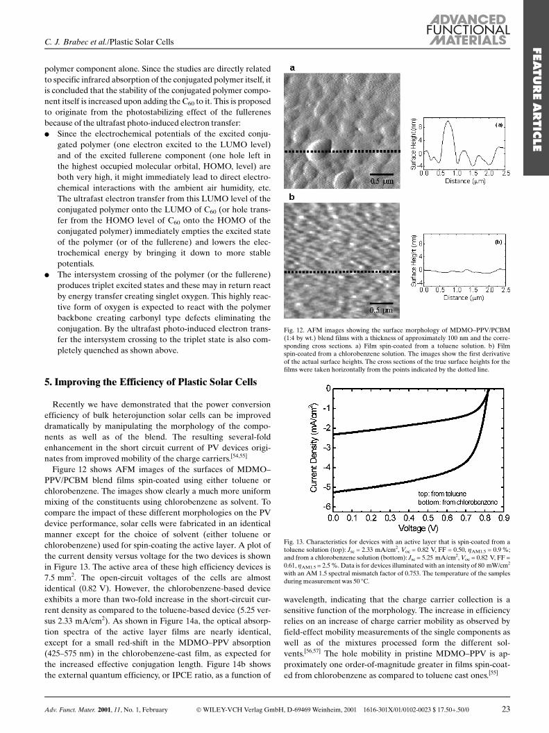
Figure 12 shows AFM images of the surfaces of MDMO±PPV/PCBM blend films spin-coated using either toluene orchlorobenzene. The images show clearly a much more uniformmixing of the constituents using chlorobenzene as solvent. Tocompare the impact of these different morphologies on the PVdevice performance, solar cells were fabricated in an identicalmanner except for the choice of solvent (either toluene orchlorobenzene) used for spin-coating the active layer. A plot ofthe current density versus voltage for the two devices is shownin Figure 13. The active area of these high efficiency devices is7.5 mm2. The open-circuit voltages of the cells are almostidentical (0.82 V). However, the chlorobenzene-based deviceexhibits a more than two-fold increase in the short-circuit cur-rent density as compared to the toluene-based device (5.25 ver-sus 2.33 mA/cm2). As shown in Figure 14a, the optical absorp-tion spectra of the active layer films are nearly identical,except for a small red-shift in the MDMO±PPV absorption(425±575 nm) in the chlorobenzene-cast film, as expected forthe increased effective conjugation length. Figure 14b showsthe external quantum efficiency, or IPCE ratio, as a function of
wavelength, indicating that the charge carrier collection is asensitive function of the morphology. The increase in efficiencyrelies on an increase of charge carrier mobility as observed byfield-effect mobility measurements of the single components aswell as of the mixtures processed form the different sol-vents.[56,57] The hole mobility in pristine MDMO±PPV is ap-proximately one order-of-magnitude greater in films spin-coat-ed from chlorobenzene as compared to toluene cast ones.[55]
Fig. 12. AFM images showing the surface morphology of MDMO±PPV/PCBM(1:4 by wt.) blend films with a thickness of approximately 100 nm and the corre-sponding cross sections. a) Film spin-coated from a toluene solution. b) Filmspin-coated from a chlorobenzene solution. The images show the first derivativeof the actual surface heights. The cross sections of the true surface heights for thefilms were taken horizontally from the points indicated by the dotted line.
Fig. 13. Characteristics for devices with an active layer that is spin-coated from atoluene solution (top): Jsc = 2.33 mA/cm2, Voc = 0.82 V, FF = 0.50, gAM1.5 = 0.9 %;and from a chlorobenzene solution (bottom): Jsc = 5.25 mA/cm2, Voc = 0.82 V, FF =0.61, gAM1.5 = 2.5 %. Data is for devices illuminated with an intensity of 80 mW/cm2
with an AM 1.5 spectral mismatch factor of 0.753. The temperature of the samplesduring measurement was 50 �C.
Adv. Funct. Mater. 2001, 11, No. 1, February Ó WILEY-VCH Verlag GmbH, D-69469 Weinheim, 2001 1616-301X/01/0102-0023 $ 17.50+.50/0 23
FEATU
RE
ARTIC
LE
C. J. Brabec et al./Plastic Solar Cells

The fill factor (FF) of solar cells is determined by
FF = ImppVmpp/IscVoc (1)
where Impp and Vmpp are the current and the voltage in themaximum power point of the I/V curve in the 4th quadrant. Ingeneral, a large serial resistance as well as a too small parallelresistance (shunt) tend to reduce the FF. From LEDs, interfacelayers like LiF or CsF and even SiOx are well known to reducethe interface barrier for electron injection at the cathode, ifthey are evaporated between the photoactive material and anAl electrode.[58] Figure 15 shows this enhancement of the diodeproperties of a MDMO±PPV/PCBM solar cell due to such aninterfacial layer. The short circuit current is left almost
unchanged and only a small increase in the open circuit voltageis observed (from 780 to 820 mV) due to the interfacial layer.The fill factor, FF, is increased from 0.5 to 0.62 by droppingdown the serial resistance of the devices from ~200±400 X to~20±50 X.
The light absorption of the device was measured (using areflection geometry) to be less than 55 % at 460 nm. This yieldsan internal quantum efficiency, or absorbed photon to con-verted electron, greater than 85 %. Since the Jsc of the deviceswas measured to have a linear dependence on the incident lightintensity for values up to 80 mW/cm2, monochromatic power
conversion efficiencies can be calculated from the IPCE data(Fig. 14b). Assuming Voc = 0.82 V and FF = 0.61 for all incidentwavelengths a power conversion efficiency of 9.5 % at 488 nmfor the chlorobenzene-based device is obtained.
One of the limiting parameters in plastic solar cells is theirmismatch to the solar spectrum. Typically, conjugated polymerssuch as MDMO±PPV, used for PVs have their peak absorptionaround 500 nm, which is clearly offset to the maximum in thephoton flux of the sun, which peaks around 700 nm. The use oflow bandgap polymers (Eg < 1.8 eV) to expand the spectralregion of bulk heterojunction solar cells can enhance thespectral photon harvesting. Figure 16 shows the spectrallyresolved photocurrent for a photodiode from low bandgappolymer (poly-(thiophene±pyrrole±thiophene±benzothiadiazole)
(PTPTB) see Table 1) with and without PCBM. Spectra arenormalized to their peak values. While the photocurrentgeneration for the pristine PTPTB device has the maximum atlow wavelengths with a small tail extending to the infrared(IR), the PTPTB/PCBM/PMMA (PMMA = poly(methyl-methacrylate)) device shows efficient charge carrier generationin the region from 500±700 nm, resembling the absorptionprofile of the polymer.[55,59] PMMA was used to improve thefilm quality. For a device with MDMO±PPV instead of PMMAas host polymer, the spectral photocurrent is observed to showcontributions from both polymers. The photocurrent of aMDMO±PPV/PCBM device is plotted as reference. Thisdemonstration shows the easy production of multiple bandgapsolar cells.
6. Outlook and Strategies
Further optimization of device performance can be achievedby optimization of the device physics:
Fig. 14. a) Optical absorption spectra of 100 nm thick MDMO±PPV/PCBM (1:4by wt.) films spin-coated onto glass substrates from either toluene (broken line)or chlorobenzene (solid line) solutions. b) IPCE spectra for PV devices usingthese films as the active layer.
Fig. 15. I/V curve in the 4th quadrant for a plastic solar cell with and without aninterfacial layer of LiF beneath the Al electrode, illuminated with 80 mW/cm2
simulated AM 1.5 radiation.
Fig. 16. Spectrally resolved photocurrent of a photodiode, where the active layer,either a low bandgap polymer PTPTB, or PTPTB/PCBM/PMMA or PTPTB/PCBM/MDMO±PPV or MDMO±PPV/PCBM is sandwiched between ITO/PEDOT and Al. Data were first calibrated to the response of a calibrated Sidiode and then normalized to their response at 400 nm.
24 Ó WILEY-VCH Verlag GmbH, D-69469 Weinheim, 2001 1616-301X/01/0102-0024 $ 17.50+.50/0 Adv. Funct. Mater. 2001, 11, No. 1, February
FEATU
RE
ARTI
CLE
C. J. Brabec et al./Plastic Solar Cells

l Optimize the choice of metallic electrodes to achieve goodohmic contacts on both sides for collection of the oppo-sitely charged photocarriers.
l Optimize the choice of the D/A pair (the energetics deter-mine the open circuit potential). In addition, the bandgapof the semiconducting polymer should be chosen for effi-cient harvesting of the solar spectrum.
l Optimize the network morphology of the phase-separatedcomposite material for enhanced transport and carrier gen-eration. The absorption and the mobility of the charge car-riers within the different components of the bulk hetero-junction have to be maximized.
In organic PV elements generally two different tasks are tobe clearly distinguished: The photo-induced charge generation(electron transfer efficiency) and the transport of createdcharges to the electrodes (charge carrier mobility). These twodifferent tasks are expected to be fulfilled by one and the samematerial simultaneously. A possible strategy is to separate thetwo tasks by using separate components in a device for thecharge transport and for the charge generation.
In this millennium, PV energy conversion will gain in mo-mentum. This clean and regenerative energy source should beutilized by exploiting all possible mechanisms, materials, anddevices. This work summarizes the progress in a special sectionof PV energy conversion: i.e., organic, bulk heterojunction so-lar cells. With ~3 % power conversion efficiency already havingbeen demonstrated, with large potential for improvement, thisapproach represents a viable route to realizing large-areaªplastic solar power conversion technologyº.
Received: October 12, 2000Final version: December 15, 2000
±[1] J. H. Burroughes, D. D. C. Bradley, A. R. Brown, R. N. Marks, K. Mackay,
R. H. Friend, P. L. Burns, A. B. Holmes, Nature 1990, 347, 539.[2] D. Braun, A. J. Heeger, Appl. Phys. Lett. 1991, 58, 1982.[3] D. Braun, A. J. Heeger, H. Kroemer, J. Electron. Mater. 1991, 20, 945.[4] N. C. Greenham, S. C. Moratti, D. D. C. Bradley, R. H. Friend, A. B.
Holmes, Nature 1993, 365, 628.
[5] I. D. Parker, J. Appl. Phys. 1994, 75, 1656.[6] G. Yu, K. Pakbaz, A. J. Heeger, Appl. Phys. Lett. 1994, 64, 3422.[7] H. Antoniadis, B. R. Hsieh, M. A. Abkowitz, M. Stolka, S. A. Jenekhe,
Polym. Prepr. 1993, 34, 490.[8] H. Antoniadis, B. R. Hsieh, M. A. Abkowitz, S. A. Jenehke, M. Stolka,
Synth. Met. 1994, 62, 265.[9] W. Rieû, S. Karg, V. Dyakonov, M. Meier, M. Schwoerer, J. Lumin. 1994,
60±61, 906.[10] N. S. Sariciftci, L. Smilowitz, A. J. Heeger, F. Wudl, Science 1992, 258, 1474.[11] N. S. Sariciftci, D. Braun, C. Zhang, V. Srdanov, A. J. Heeger, G. Stucky, F.
Wudl, Appl. Phys. Lett. 1993, 62, 585.[12] G. Yu, J. Gao, J. C. Hummelen, F. Wudl, A. J. Heeger, Science 1995, 270,
1789.[13] J. J. M. Halls, C. A. Walsh, N. C. Greenham, E. A. Marseglia, R. H. Friend,
S. C. Moratti, A. B. Holmes, Nature 1995, 376, 498.[14] L. Smilowitz, N. S. Sariciftci, R. Wu, C. Gettinger, A. J. Heeger, F. Wudl,
Phys. Rev. B 1993, 47, 13 835.[15] B. Kraabel, J. C. Hummelen, D. Vacar, D. Moses, N. S. Sariciftci, A. J. Hee-
ger, F. Wudl, J. Chem. Phys. 1996, 104, 4267.[16] N. S. Sariciftci, A. J. Heeger, Int. J. Mod. Phys. B 1994, 8, 237.[17] N. S. Sariciftci, Prog. Quantum Electron. 1995, 19, 131.[18] X. Wei, Z. V. Vardeny, N. S. Sariciftci, A. J. Heeger, Phys. Rev. B 1996, 53,
2187.[19] S. Morita, A. A. Zakhidov, K. Yoshino, Solid State Commun. 1992, 82, 249.[20] K. Yoshino, X. H. Yin, S. Morita, T. Kawai, A. A. Zakhidov, Solid State
Commun. 1993, 85, 85.[21] S. Morita, A. A. Zakhidov, K. Yoshino, Jpn. J. Appl. Phys. 1993, 32, L873.[22] K. Yoshino, T. Akashi, K. Yoshimoto, S. Morita, R. Sugimoto, A. A. Zakhi-
dov, Solid State Commun. 1994, 90, 41.[23] J. J. M. Halls, R. H. Friend, Synth. Met. 1997, 85, 1307.[24] G. Yu, A. J. Heeger, J. Appl. Phys. 1995, 78, 4510.[25] N. S. Sariciftci, A. J. Heeger, in Handbook of Organic Conductive Mole-
cules and Polymers, Vol. 1 (Ed: H. S. Nalwa), Wiley, New York 1996,pp. 414±450.
[26] B. Kraabel, C. H. Lee, D. McBranch, D. Moses, N. S. Sariciftci, A. J. Hee-ger, Chem. Phys. Lett. 1993, 213, 389.
[27] B. Kraabel, D. McBranch, N. S. Sariciftci, D. Moses, A. J. Heeger, Phys.Rev. B 1994, 50, 18 543.
[28] C. J. Brabec, G. Zerza, G. Cerullo, S. De Silvestri, S. Luzzati, J. C. Humme-len, N. S. Sariciftci, unpublished.
[29] C. H. Lee, G. Yu, N. S. Sariciftci, D. Moses, K. Pakbaz, C. Zhang, A. J. Hee-ger, F. Wudl, Phys. Rev. B 1993, 48, 15 425.
[30] P. M. Allemand, G. Srdanov, A. Koch, K. Khemani, F. Wudl, Y. Rubin,F. N. Diederich, M. M. Alvarez, S. J. Anz, R. L. Whetten, J. Am. Chem.Soc. 1991, 113, 2780.
[31] V. Dyakonov, G. Zoriniants, M. C. Scharber, C. J. Brabec, R. A. J. Janssen,J. C. Hummelen, N. S. Sariciftci, Phys. Rev. B 1999, 59, 8019.
[32] H. Meier, Organic Semiconductors, Verlag-Chemie, Weinheim 1974.[33] C. W. Tang, Appl. Phys. Lett. 1986, 48, 183.[34] J. Simon, J.-J. Andre, Molecular Semiconductors, Springer, Berlin 1985.[35] C. J. Brabec, N. S. Sariciftci, in Semiconducting Polymers (Eds: G. Had-
ziioannou, P. F. van Hutten), WILEY-VCH, Weinheim 1999, Ch. 15,pp. 515±560.
[36] J. Kanicki, in Handbook of Conducting Polymers, Vol. 1 (Ed: T. A.Skotheim), Marcel Dekker, New York 1986, pp. 543±660.
[37] M. Kaneko, in Handbook of Organic Conductive Molecules and Polymers,Vol. 4 (Ed: H. S. Nalwa), Wiley, New York 1997, p. 661.
[38] B. O'Regan, M. A. Grätzel, Nature 1991, 353, 737.[39] U. Bach, D. Lupo, P. Comte, J. E. Moser, F. Weissörtel, J. Salbeck, H. Spreit-
zer, M. Grätzel, Nature 1998, 395, 583.[40] Y. Yamashita, W. Takashima, K. Kaneto, Jpn. J. Appl. Phys. 1993, 32,
L1017.[41] D. Wöhrle, D. Meissner, Adv. Mater. 1991, 3, 129.[42] J. Rostalski, D. Meissner, Sol. Energy Mater. Sol. Cells 2000, 61, 87.[43] J. Rostalski, D. Meissner, Sol. Energy Mater. Sol. Cells 2000, 63, 37.[44] T. Tsuzuki, Y. Shirota, J. Rostalski, D. Meissner, Sol. Energy Mater. Sol.
Cells 2000, 61, 1.[45] L. S. Roman, W. Mammo, L. A. A. Pettersson, M. R. Andersson, O. Inga-
näs, Adv. Mater. 1998, 10, 774.[46] J. J. M. Halls, R. H. Friend, Synth. Met. 1997, 85, 1307.[47] G. Yu, C. Zhang, A. J. Heeger, Appl. Phys. Lett. 1994, 64, 1540.[48] H. Antoniadis, B. R. Hsieh, M. A. Abkowitz, M. Stolka, S. A. Jenekhe,
Polym. Prepr. 1993, 34, 490.[49] S. Karg, W. Riess, V. Dyakonov, M. Schwoerer, Synth. Met. 1993, 54, 427.[50] M. Granstrom, K. Petritsch, A. C. Arias, A. Lux, M. R. Andersson, R. H.
Friend, Nature 1998, 395, 257.[51] N. C. Greenham, S. C. Moratti, D. D. C. Bradley, R. H. Friend, A. B.
Holmes, Nature 1993, 365, 628.
Table 1. Abbreviation and structure of common conjugated polymers as well asacceptor type molecules.
Adv. Funct. Mater. 2001, 11, No. 1, February Ó WILEY-VCH Verlag GmbH, D-69469 Weinheim, 2001 1616-301X/01/0102-0025 $ 17.50+.50/0 25
FEATU
RE
ARTIC
LE
C. J. Brabec et al./Plastic Solar Cells

[52] H. Neugebauer, C. J. Brabec, J. C. Hummelen, N. S. Sariciftci, Sol. EnergyMater. Sol. Cells 2000, 61, 35.
[53] H. Neugebauer, C. J. Brabec, J. C. Hummelen, R. A. J. Janssen, N. S. Sari-ciftci, Synth. Met. 1999, 102, 1002.
[54] S. E. Shaheen, C. J. Brabec, F. Padinger, T. Fromherz, J. C. Hummelen,N. S. Sariciftci, unpublished.
[55] C. J. Brabec, S. E. Shaheen. T. Fromherz, F. Padinger, J. C. Hummelen,A. Dhanabalan, R. A. J. Janssen, N. S. Sariciftci, Synth. Met., in press.
[56] W. Geens, S. E. Shaheen, C. J. Brabec, J. Poortmans, N. S. Sariciftci, inElectronic Properties of Novel Materials (Eds: H. Kuzmany, J. Fink,M. Mehring, S. Roth), IOP, Bristol, UK, in press.
[57] S. E. Shaheen, C. J. Brabec, N. S. Sariciftci, W. Geens, J. Poortmans, unpub-lished.
[58] G. E. Jabbour, Y. Kawabe, S. E. Shaheen, J. F. Wang, M. M. Morrell,B. Kippelen, N. Peyghamberian, Appl. Phys. Lett. 1997, 71, 1762.
[59] S. E. Shaheen, D. Vangeneugden, R. Kiebooms, D. Vanderzande, T. From-herz, F. Padinger, C. J. Brabec, N. S. Sariciftci, Synth. Met., in press.
______________________
26 Ó WILEY-VCH Verlag GmbH, D-69469 Weinheim, 2001 1616-301X/01/0102-0026 $ 17.50+.50/0 Adv. Funct. Mater. 2001, 11, No. 1, February
FEATU
RE
ARTI
CLE
C. J. Brabec et al./Plastic Solar Cells