Plasmonics: Application-oriented fabrication Part 3 ... · August 25, 2013 ICQNM 2013 Barcelona,...
69
August 25, 2013 ICQNM 2013 Barcelona, Spain 1 Plasmonics: Application-oriented fabrication Part 3. Fabrication methods Victor Ovchinnikov Department of Aalto Nanofab Aalto University Espoo, Finland
-
Upload
nguyendang -
Category
Documents
-
view
214 -
download
0
Transcript of Plasmonics: Application-oriented fabrication Part 3 ... · August 25, 2013 ICQNM 2013 Barcelona,...
August 25, 2013 ICQNM 2013 Barcelona, Spain 1
Plasmonics: Application-oriented fabrication
Part 3. Fabrication methods
Victor Ovchinnikov
Department of Aalto NanofabAalto UniversityEspoo, Finland
Motivation
• The first part - introduction to plasmonics
• The second part - analysis of fabrication problems for plasmonic devices
• This part - application of different methods in fabrication of plasmonic devices
August 25, 2013 ICQNM 2013 Barcelona, Spain 2
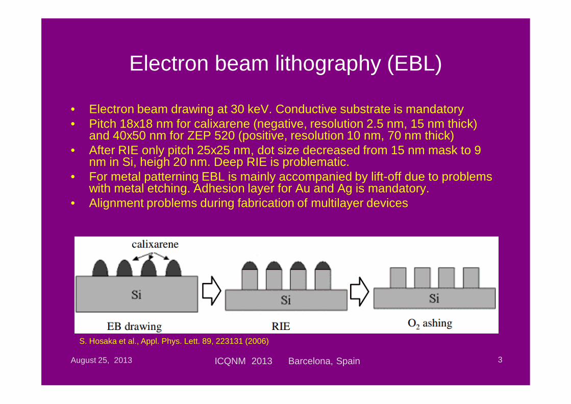
Electron beam lithography (EBL)
• Electron beam drawing at 30 keV. Conductive substrate is mandatory• Pitch 18x18 nm for calixarene (negative, resolution 2.5 nm, 15 nm thick)
and 40x50 nm for ZEP 520 (positive, resolution 10 nm, 70 nm thick)• After RIE only pitch 25x25 nm, dot size decreased from 15 nm mask to 9
nm in Si, heigh 20 nm. Deep RIE is problematic.• For metal patterning EBL is mainly accompanied by lift-off due to problems
with metal etching. Adhesion layer for Au and Ag is mandatory.• Alignment problems during fabrication of multilayer devices
August 25, 2013 ICQNM 2013 Barcelona, Spain 3
S. Hosaka et al., Appl. Phys. Lett. 89, 223131 (2006)

Nanohole array by EBL
• Deposition of a conductive layer (3 nm of Cr or Ti) to avoid substrate charging.
• 500 nm photoresist (Negative Tone) was spin-coated and soft-baked on the conductive layer.
• Pattern of nano-hole arrays was written with the EBL machine
• (LEO, 1530 e-beam lithography) and followed by development. The adhesion layer (5-10 nm of Ti) was deposited
• Deposition of a 100 nm gold layer.• Sacrificial mask layer (PR pillars)
was lifted off
August 25, 2013 ICQNM 2013 Barcelona, Spain 4
Pyrex, 100 nm thick Au with 200 nm holes
19 December 2011 / Vol. 19, No. 27 / OPTICS EXPRESS 26186
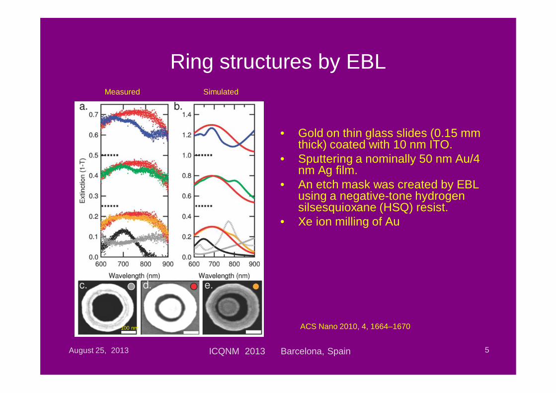
Ring structures by EBL
• Gold on thin glass slides (0.15 mm thick) coated with 10 nm ITO.
• Sputtering a nominally 50 nm Au/4 nm Ag lm.
• An etch mask was created by EBL using a negative-tone hydrogen silsesquioxane (HSQ) resist.
• Xe ion milling of Au
August 25, 2013 ICQNM 2013 Barcelona, Spain 5
100 nm
Measured Simulated
ACS Nano 2010, 4, 1664–1670
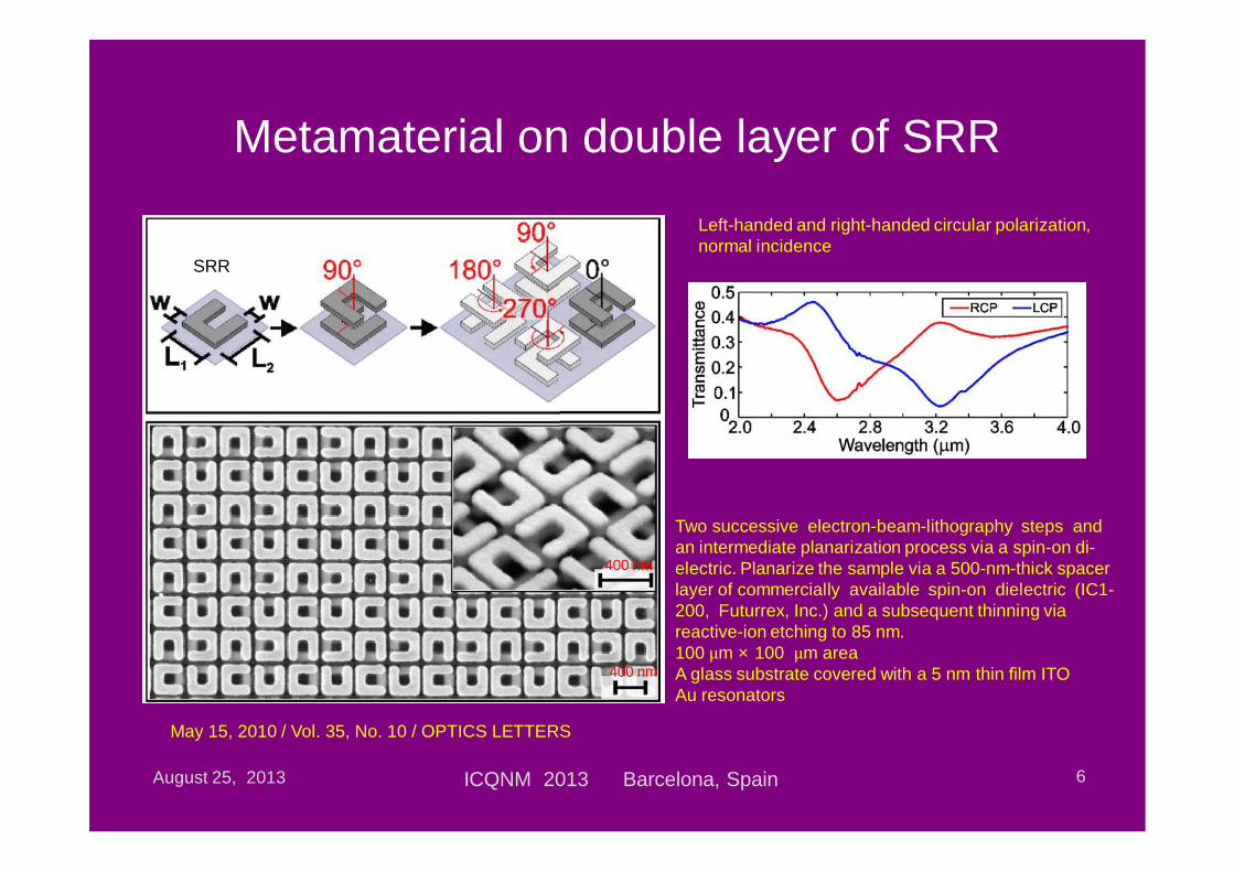
Metamaterial on double layer of SRR
August 25, 2013 ICQNM 2013 Barcelona, Spain 6
Two successive electron-beam-lithography steps and an intermediate planarization process via a spin-on di-electric. Planarize the sample via a 500-nm-thick spacer layer of commercially available spin-on dielectric (IC1-200, Futurrex, Inc.) and a subsequent thinning via reactive-ion etching to 85 nm.100 m × 100 m areaA glass substrate covered with a 5 nm thin lm ITOAu resonators
400 nm
400 nm
Left-handed and right-handed circular polarization,normal incidence
May 15, 2010 / Vol. 35, No. 10 / OPTICS LETTERS
SRR
FIB
• FIB lithography is superior to EBL:– Higher resolution– Higher resist sensitivity
• Additionally to EBL:– Local ion beam etching (subtractive lithography)
• 3D patterning– Local deposition of materials (additive lithography)– Local ion implantation
• 3D patterning– Local ion-induced mixing– Direct patterning of hard mask layers
• Multi-beam systems• Conductive layer on the substrate is mandatory• Redeposition of sputtered material on the sampleAugust 25, 2013 ICQNM 2013 Barcelona, Spain 7
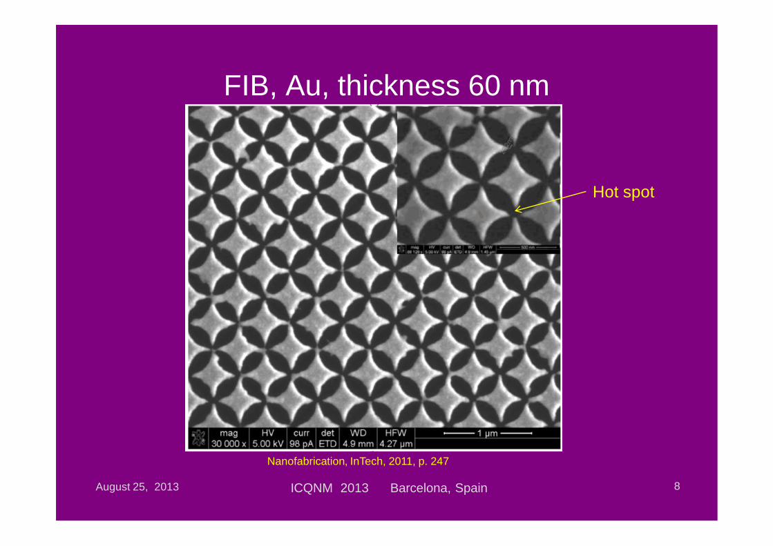
FIB, Au, thickness 60 nm
August 25, 2013 ICQNM 2013 Barcelona, Spain 8
Nanofabrication, InTech, 2011, p. 247
Hot spot
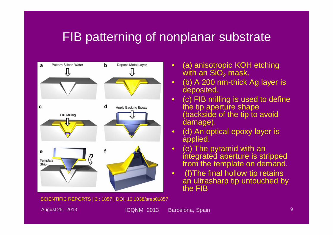
FIB patterning of nonplanar substrate
• (a) anisotropic KOH etching with an SiO2 mask.
• (b) A 200 nm-thick Ag layer is deposited.
• (c) FIB milling is used to define the tip aperture shape (backside of the tip to avoid damage).
• (d) An optical epoxy layer is applied.
• (e) The pyramid with an integrated aperture is stripped from the template on demand.
• (f)The final hollow tip retains an ultrasharp tip untouched by the FIB
August 25, 2013 ICQNM 2013 Barcelona, Spain 9
SCIENTIFIC REPORTS | 3 : 1857 | DOI: 10.1038/srep01857

Plasmonic nanofocusing structures by FIB
August 25, 2013 ICQNM 2013 Barcelona, Spain 10
SCIENTIFIC REPORTS | 3 : 1857 | DOI: 10.1038/srep01857

Interference lithography (IL)
• Wafer scale• High laser power, more than 1 W• Laser coherence length more than 1 m• Transparent substrate or absorbing layer below
light sensetive layer (mask)• PR patterning above metal is impossible• Critical dimensions are limited by laser
wavelength, but not less than 20 nm• Limited to patterning arrayed features only with
narrow range of size to spacing ratioAugust 25, 2013 ICQNM 2013 Barcelona, Spain 11
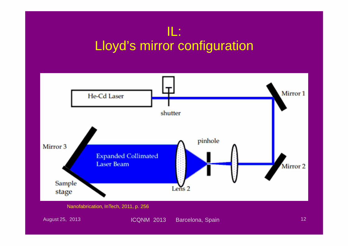
IL:Lloyd’s mirror configuration
August 25, 2013 ICQNM 2013 Barcelona, Spain 12
Nanofabrication, InTech, 2011, p. 256
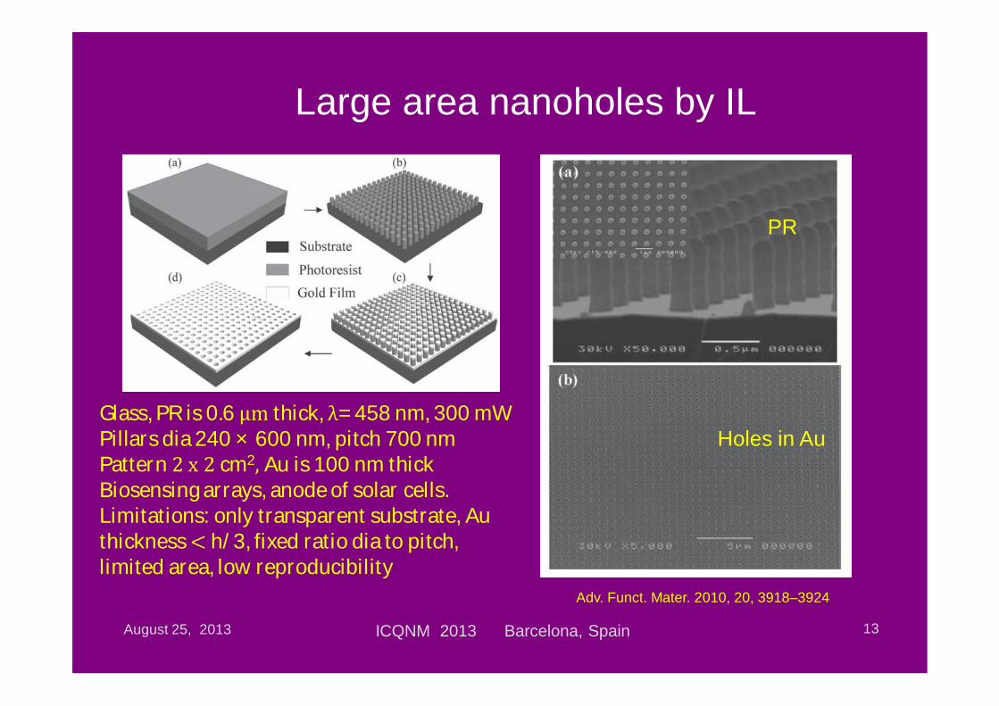
Large area nanoholes by IL
August 25, 2013 ICQNM 2013 Barcelona, Spain 13
Adv. Funct. Mater. 2010, 20, 3918–3924
Glass, PR is 0.6 thick, =458 nm, 300 mWPillars dia 240 × 600 nm, pitch 700 nmPattern cm2 Au is 100 nm thickBiosensing arrays, anode of solar cells.Limitations: only transparent substrate, Authickness h/3, fixed ratio dia to pitch,limited area, low reproducibility
PR
Holes in Au
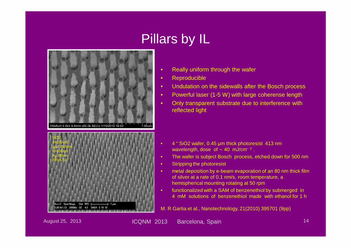
Pillars by IL
• 4 “ SiO2 wafer, 0.45 m thick photoresist 413 nm wavelength, dose of 40 mJ/cm 2 .
• The wafer is subject Bosch process, etched down for 500 nm• Stripping the photoresist• metal deposition by e-beam evaporation of an 80 nm thick lm
of silver at a rate of 0.1 nm/s, room temperature, a hemispherical mounting rotating at 50 rpm
• functionalized with a SAM of benzenethiol by submerged in 4 mM solutions of benzenethiol made with ethanol for 1 h
• Really uniform through the wafer• Reproducible• Undulation on the sidewalls after the Bosch process• Powerful laser (1-5 W) with large coherense length• Only transparent substrate due to interference with
reflected light
August 25, 2013 ICQNM 2013 Barcelona, Spain 14
M. R Gartia et al., Nanotechnology, 21(2010) 395701 (9pp)
SiO2d=150nmgap 350 nmh=500nmAg 80nmEF=5·107
.
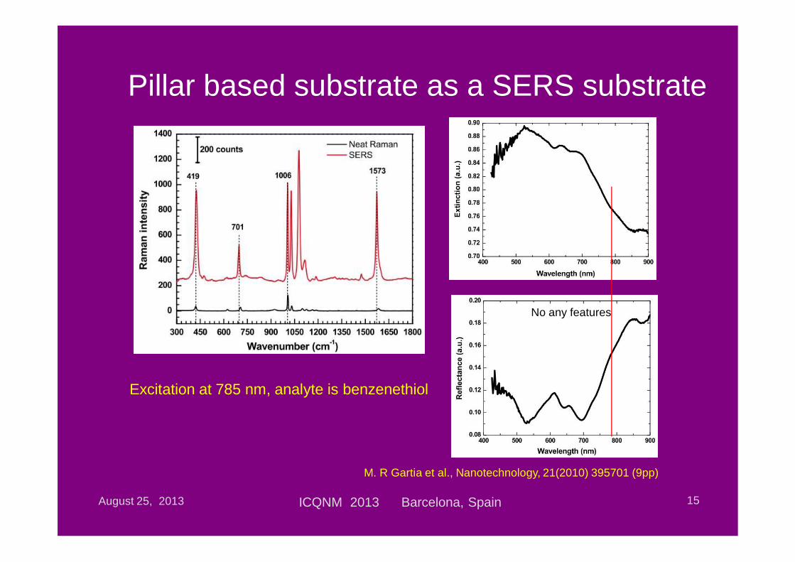
Pillar based substrate as a SERS substrate
August 25, 2013 ICQNM 2013 Barcelona, Spain 15
No any features
M. R Gartia et al., Nanotechnology, 21(2010) 395701 (9pp)
Excitation at 785 nm, analyte is benzenethiol

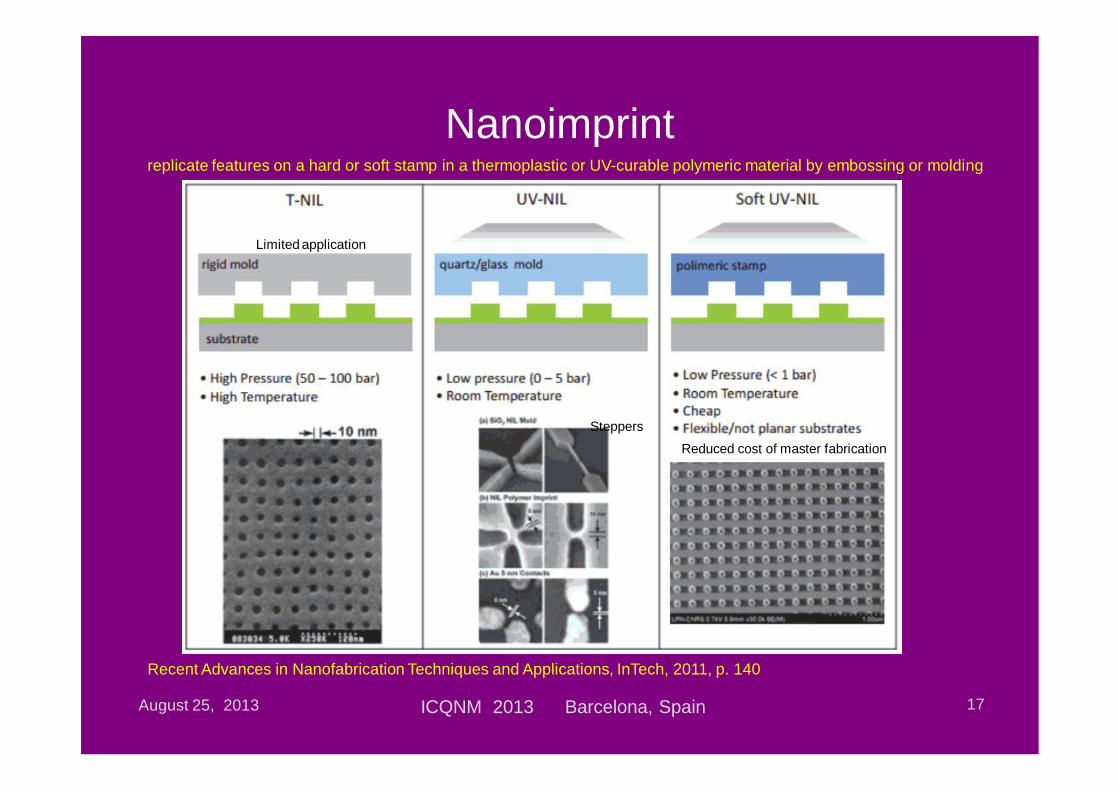
Nanoimprint Lithography (NIL)
• Thermal assisted (T-NIL), 50 nm pitch, 100C above Tg, 50-100 bar, 1995.
• microContact Printing (mCP), 1993• UV-NIL, 5 nm features, 0-5 bar• Soft UV nanoimprint lithography (Soft UV-NIL),
sub-50 nm range
August 25, 2013 ICQNM 2013 Barcelona, Spain 16
Nanoimprint
August 25, 2013 ICQNM 2013 Barcelona, Spain 17
Recent Advances in Nanofabrication Techniques and Applications, InTech, 2011, p. 140
Limited application
Steppers
Reduced cost of master fabrication
replicate features on a hard or soft stamp in a thermoplastic or UV-curable polymeric material by embossing or molding
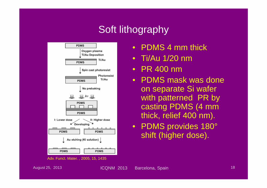
Soft lithography
• PDMS 4 mm thick• Ti/Au 1/20 nm• PR 400 nm• PDMS mask was done
on separate Si wafer with patterned PR by casting PDMS (4 mm thick, relief 400 nm).
• PDMS provides 180°shift (higher dose).
August 25, 2013 ICQNM 2013 Barcelona, Spain 18
Adv. Funct. Mater. , 2005, 15, 1435
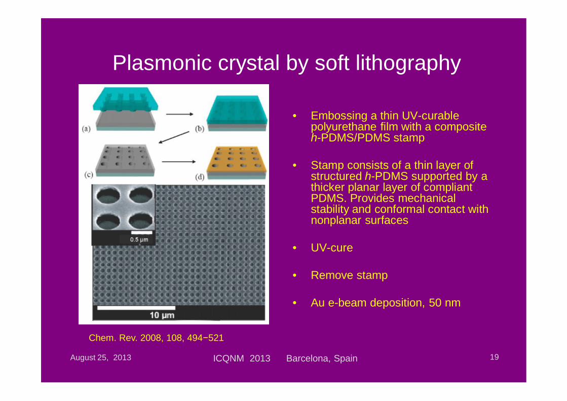
Plasmonic crystal by soft lithography
• Embossing a thin UV-curable polyurethane film with a composite h-PDMS/PDMS stamp
• Stamp consists of a thin layer of structured h-PDMS supported by a thicker planar layer of compliant PDMS. Provides mechanical stability and conformal contact with nonplanar surfaces
• UV-cure
• Remove stamp
• Au e-beam deposition, 50 nm
August 25, 2013 ICQNM 2013 Barcelona, Spain 19
Chem. Rev. 2008, 108, 494 521

Large-area hole array by soft lithography
• An array of posts of positive photoresist with diameters of 250 nm is patterned by phase-shifting hotolithography using a conformable composite PDMS photomask
• A thin layer of Cr is then deposited by e-beam evaporation followed by removal of the photoresist posts
• The exposed Si is then anisotropically etched using a KOH/isopropyl alcohol (IPA) solution to produce pyramidal-shaped voids
• A layer of Au can then be deposited by e-beam evaporation
August 25, 2013 ICQNM 2013 Barcelona, Spain 20
500 nm
2 m
Chem. Rev. 2008, 108, 494 521
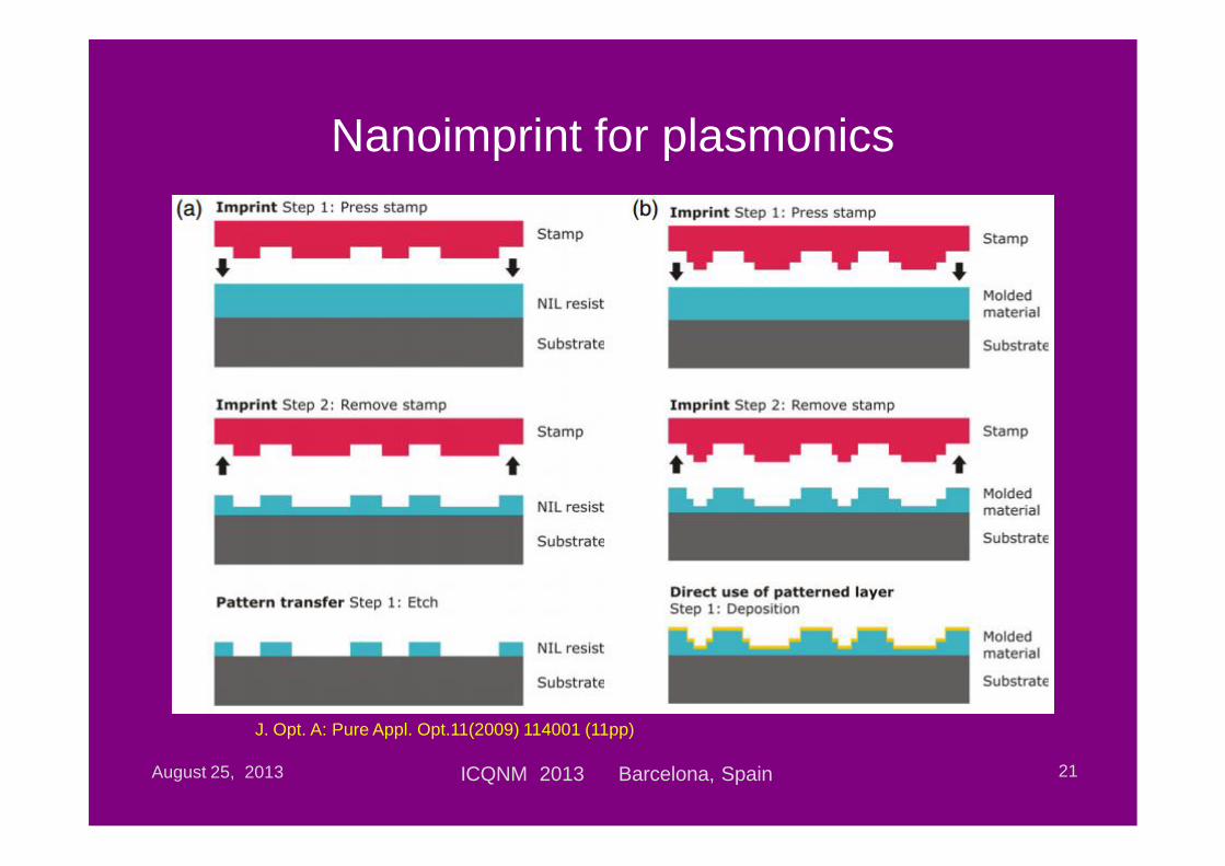
Nanoimprint for plasmonics
August 25, 2013 ICQNM 2013 Barcelona, Spain 21
J. Opt. A: Pure Appl. Opt.11(2009) 114001 (11pp)
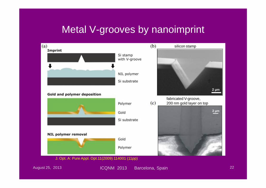
Metal V-grooves by nanoimprint
August 25, 2013 ICQNM 2013 Barcelona, Spain 22
J. Opt. A: Pure Appl. Opt.11(2009) 114001 (11pp)
silicon stamp
fabricated V-groove,200 nm gold layer on top
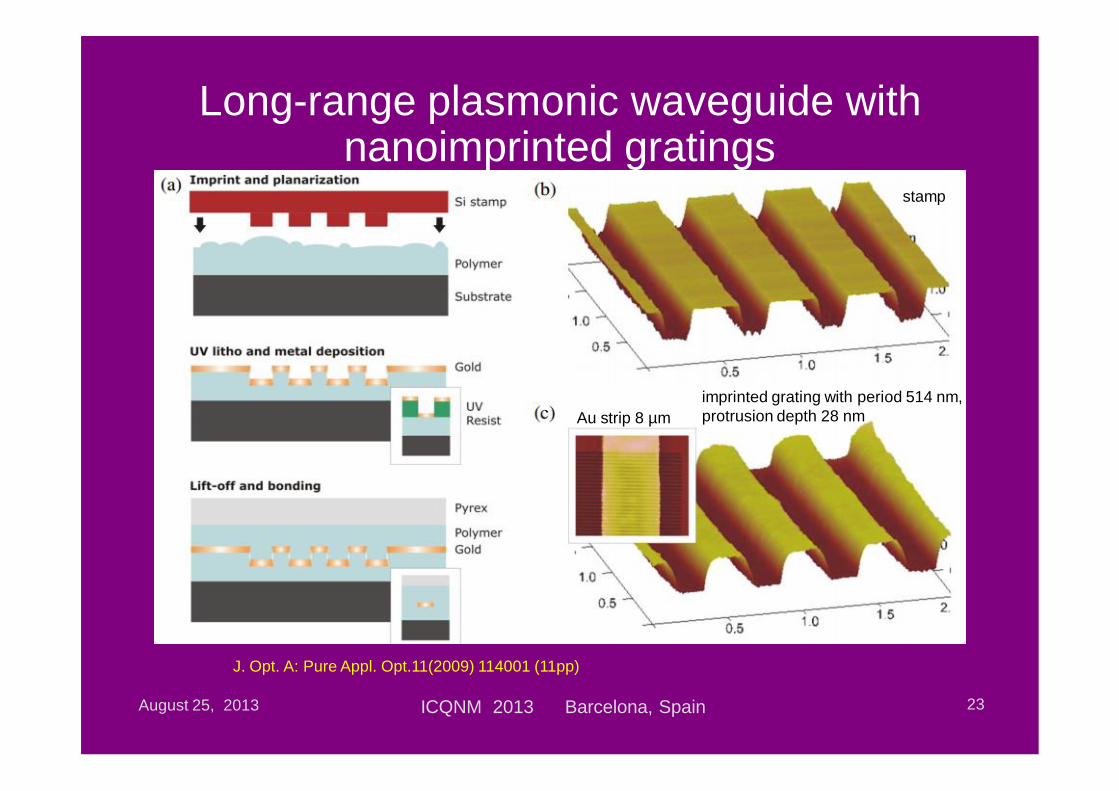
Long-range plasmonic waveguide with nanoimprinted gratings
August 25, 2013 ICQNM 2013 Barcelona, Spain 23
J. Opt. A: Pure Appl. Opt.11(2009) 114001 (11pp)
Au strip 8 µm
stamp
imprinted grating with period 514 nm,protrusion depth 28 nm

Nanoimprint
• Beyond the limitations set by light diffraction or beam scattering
• Replication in more than two levels, i.e. creating pattern with complicate profile (lithography gives only rectangles)
• Wafer scale processing• Can be applied only to the planar surface
without relief
August 25, 2013 ICQNM 2013 Barcelona, Spain 24
Nanoimprint
August 25, 2013 ICQNM 2013 Barcelona, Spain 25
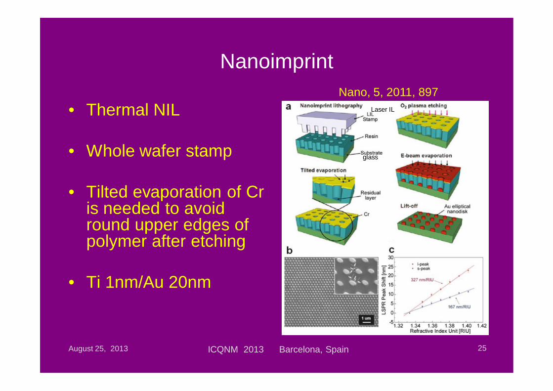
• Thermal NIL
• Whole wafer stamp
• Tilted evaporation of Cr is needed to avoid round upper edges of polymer after etching
• Ti 1nm/Au 20nm
Nano, 5, 2011, 897
glass
Laser IL
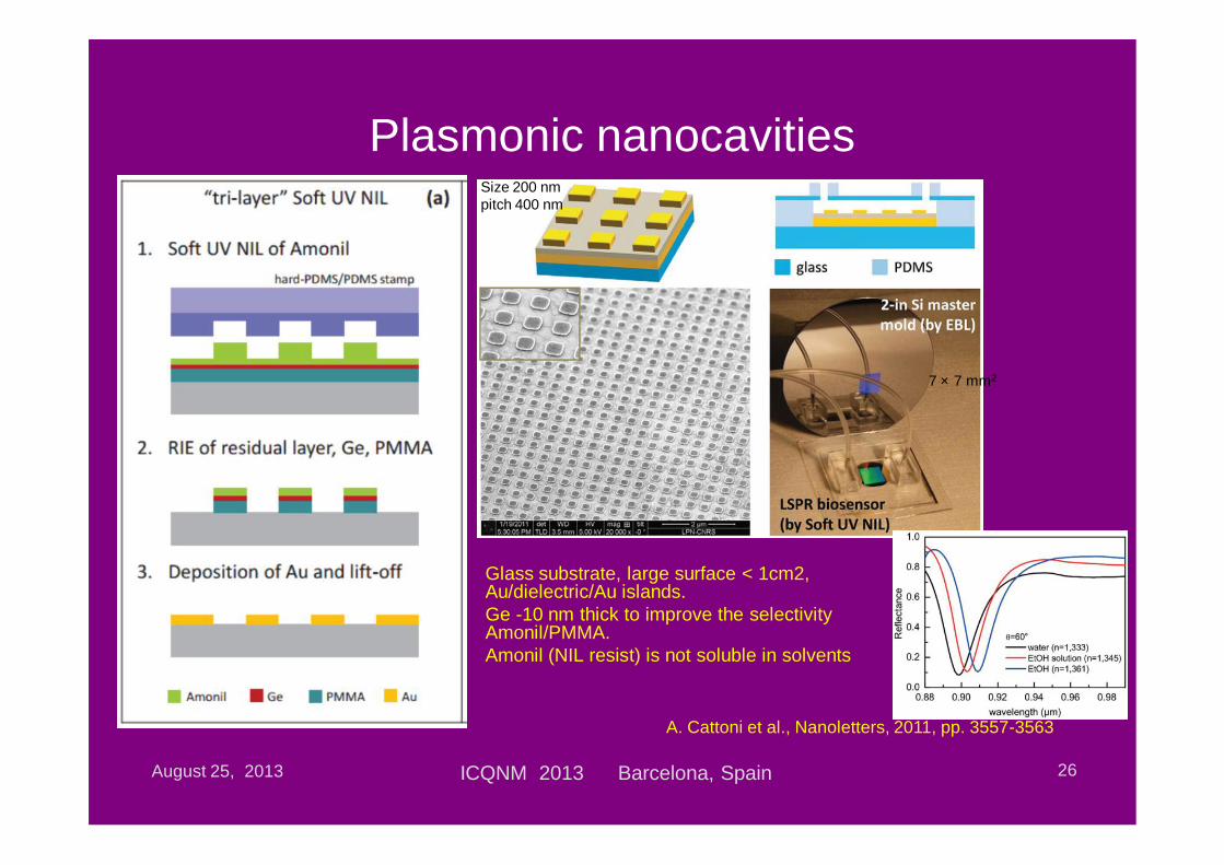
Plasmonic nanocavities
Glass substrate, large surface < 1cm2, Au/dielectric/Au islands.Ge -10 nm thick to improve the selectivity Amonil/PMMA.Amonil (NIL resist) is not soluble in solvents
August 25, 2013 ICQNM 2013 Barcelona, Spain 26
A. Cattoni et al., Nanoletters, 2011, pp. 3557-3563
Size 200 nmpitch 400 nm
7 × 7 mm2

Template assisted lithography
• Porous anodic Al2O3
• Nanosphere lithography (NSL)• Colloidal lithography• Shadow mask (stencil)• Template stripping
August 25, 2013 ICQNM 2013 Barcelona, Spain 27
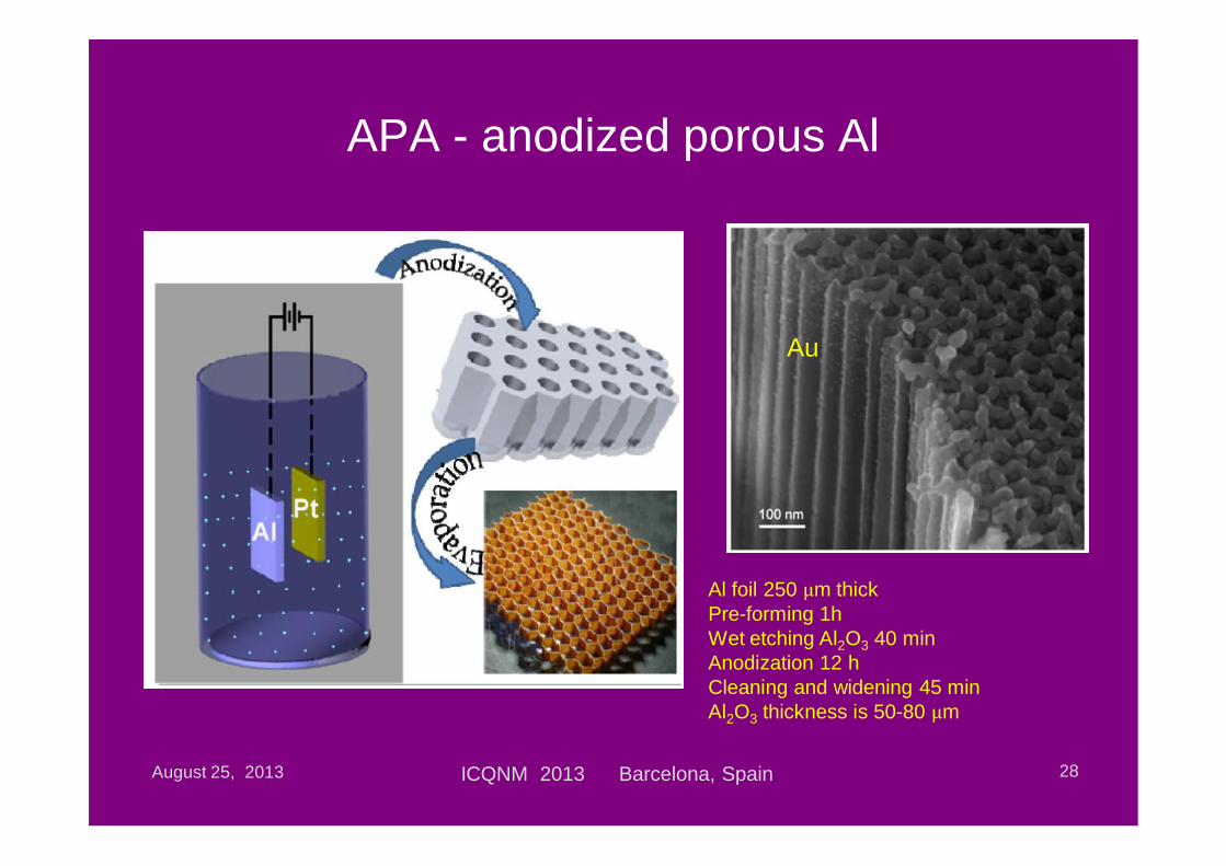
APA - anodized porous Al
August 25, 2013 ICQNM 2013 Barcelona, Spain 28
Al foil 250 m thickPre-forming 1hWet etching Al2O3 40 minAnodization 12 hCleaning and widening 45 minAl2O3 thickness is 50-80 m
Au
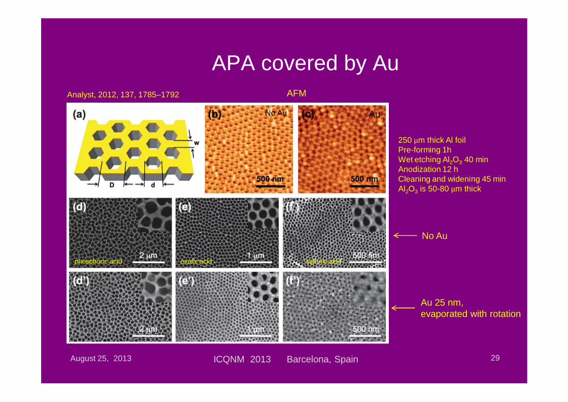
APA covered by Au
August 25, 2013 ICQNM 2013 Barcelona, Spain 29
AFM
No Au
Au 25 nm,evaporated with rotation
No Au Au
Analyst, 2012, 137, 1785–1792
250 m thick Al foilPre-forming 1hWet etching Al2O3 40 minAnodization 12 hCleaning and widening 45 minAl2O3 is 50-80 m thick
phosphoric acid oxalic acid sulfuric acid
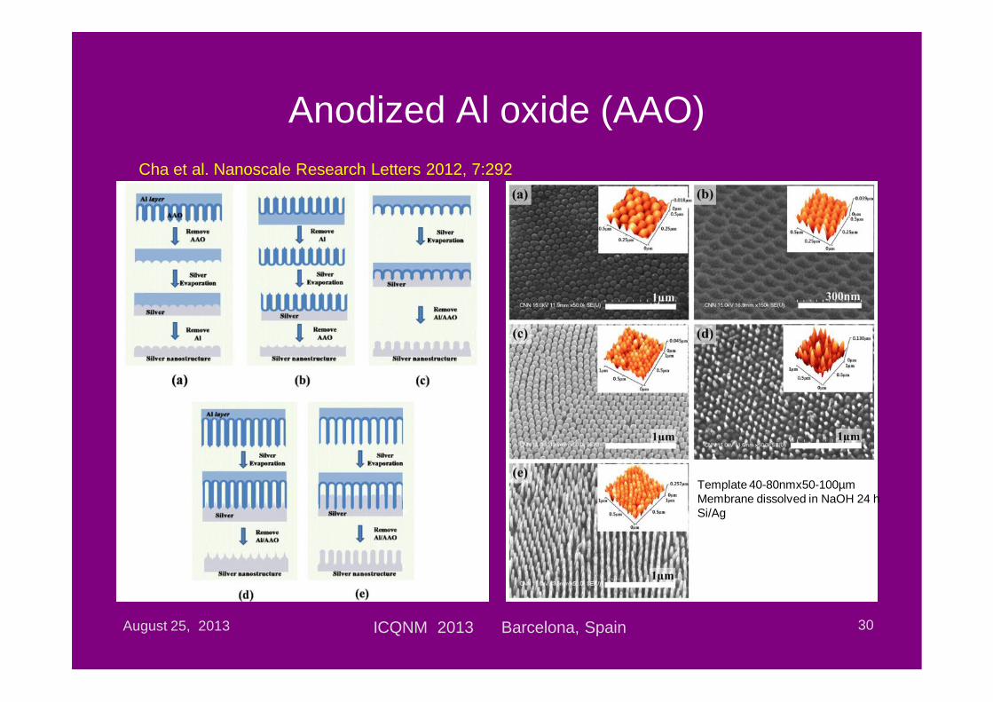
Anodized Al oxide (AAO)
August 25, 2013 ICQNM 2013 Barcelona, Spain 30
Cha et al. Nanoscale Research Letters 2012, 7:292
Template 40-80nmx50-100µmMembrane dissolved in NaOH 24 hSi/Ag
Hemispherical nanostructures
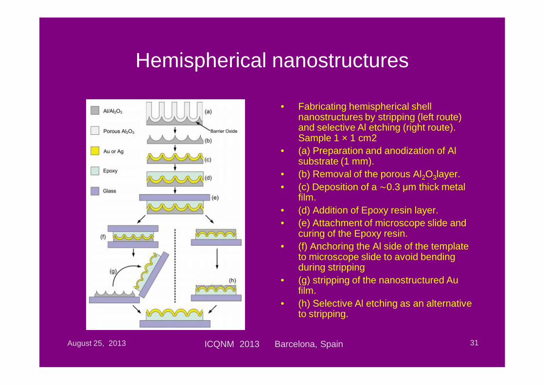
• Fabricating hemispherical shell nanostructures by stripping (left route) and selective Al etching (right route). Sample 1 × 1 cm2
• (a) Preparation and anodization of Al substrate (1 mm).
• (b) Removal of the porous Al2O3layer.• (c) Deposition of a 0.3 m thick metal
film.• (d) Addition of Epoxy resin layer.• (e) Attachment of microscope slide and
curing of the Epoxy resin.• (f) Anchoring the Al side of the template
to microscope slide to avoid bending during stripping
• (g) stripping of the nanostructured Au film.
• (h) Selective Al etching as an alternative to stripping.
August 25, 2013 ICQNM 2013 Barcelona, Spain 31

Hemispherical
August 25, 2013 ICQNM 2013 Barcelona, Spain 32
AFM image (1×1 m) of hollows in a template
Au hemispherical shellsJ. Phys. Chem. C, 2011, 115 (13), pp 5552–5560
Anodized Al
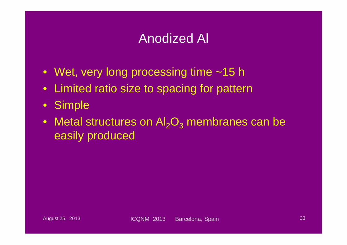
• Wet, very long processing time ~15 h• Limited ratio size to spacing for pattern• Simple• Metal structures on Al2O3 membranes can be
easily produced
August 25, 2013 ICQNM 2013 Barcelona, Spain 33
Nanosphere lithography (NSL) I
August 25, 2013 ICQNM 2013 Barcelona, Spain 34
Stiles P.L. et all, Annual Review of Analytical Chemistry, 1, 2008, p.601-26
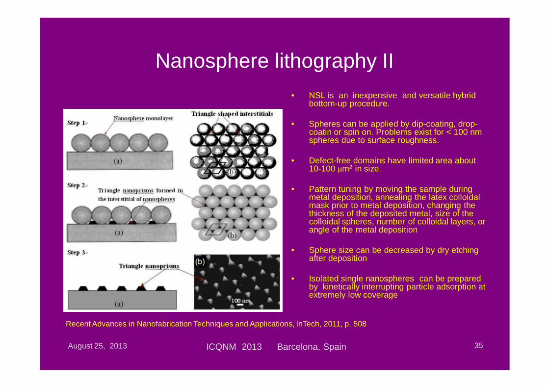
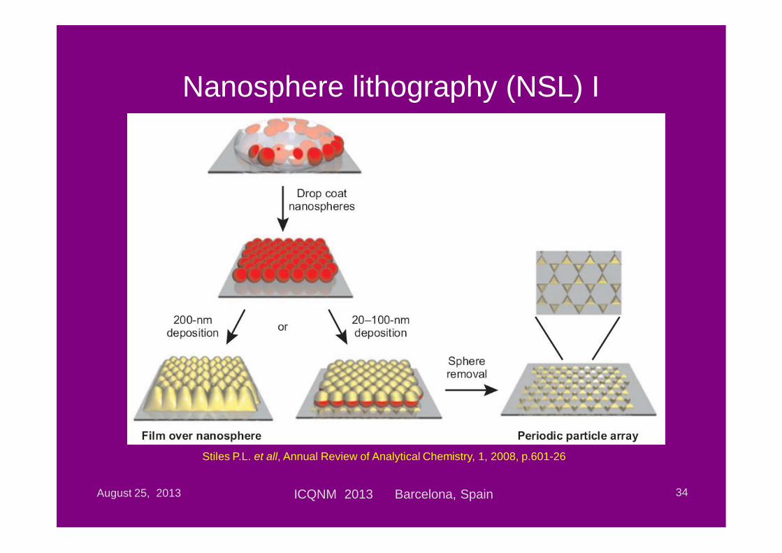
Nanosphere lithography II• NSL is an inexpensive and versatile hybrid
bottom-up procedure.
• Spheres can be applied by dip-coating, drop-coatin or spin on. Problems exist for < 100 nm spheres due to surface roughness.
• Defect-free domains have limited area about 10-100 m2 in size.
• Pattern tuning by moving the sample during metal deposition, annealing the latex colloidal mask prior to metal deposition, changing the thickness of the deposited metal, size of the colloidal spheres, number of colloidal layers, or angle of the metal deposition
• Sphere size can be decreased by dry etching after deposition
• Isolated single nanospheres can be prepared by kinetically interrupting particle adsorption at extremely low coverage
August 25, 2013 ICQNM 2013 Barcelona, Spain 35
Recent Advances in Nanofabrication Techniques and Applications, InTech, 2011, p. 508
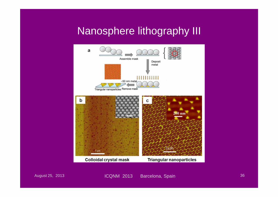
Nanosphere lithography III
August 25, 2013 ICQNM 2013 Barcelona, Spain 36
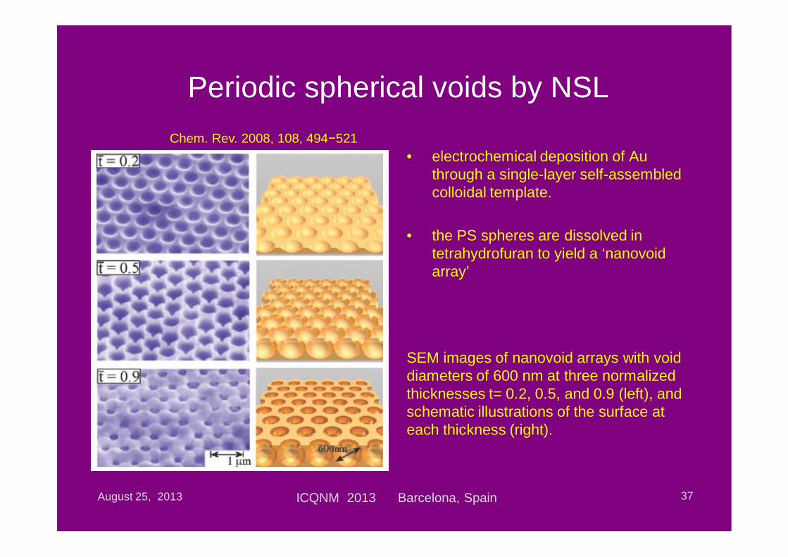
Periodic spherical voids by NSL
• electrochemical deposition of Au through a single-layer self-assembled colloidal template.
• the PS spheres are dissolved in tetrahydrofuran to yield a ‘nanovoidarray’
SEM images of nanovoid arrays with void diameters of 600 nm at three normalized thicknesses t= 0.2, 0.5, and 0.9 (left), and schematic illustrations of the surface at each thickness (right).
August 25, 2013 ICQNM 2013 Barcelona, Spain 37
Chem. Rev. 2008, 108, 494 521
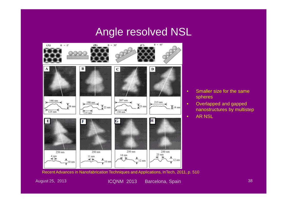
Angle resolved NSL
• Smaller size for the same spheres
• Overlapped and gapped nanostructures by multistep
• AR NSL
August 25, 2013 ICQNM 2013 Barcelona, Spain 38
Recent Advances in Nanofabrication Techniques and Applications, InTech, 2011, p. 510
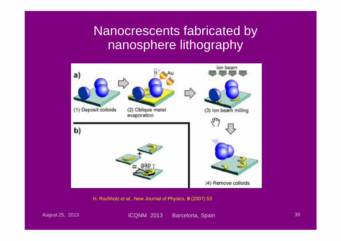
Nanocrescents fabricated bynanosphere lithography
August 25, 2013 ICQNM 2013 Barcelona, Spain 39
H. Rochholz et al., New Journal of Physics, 9 (2007) 53
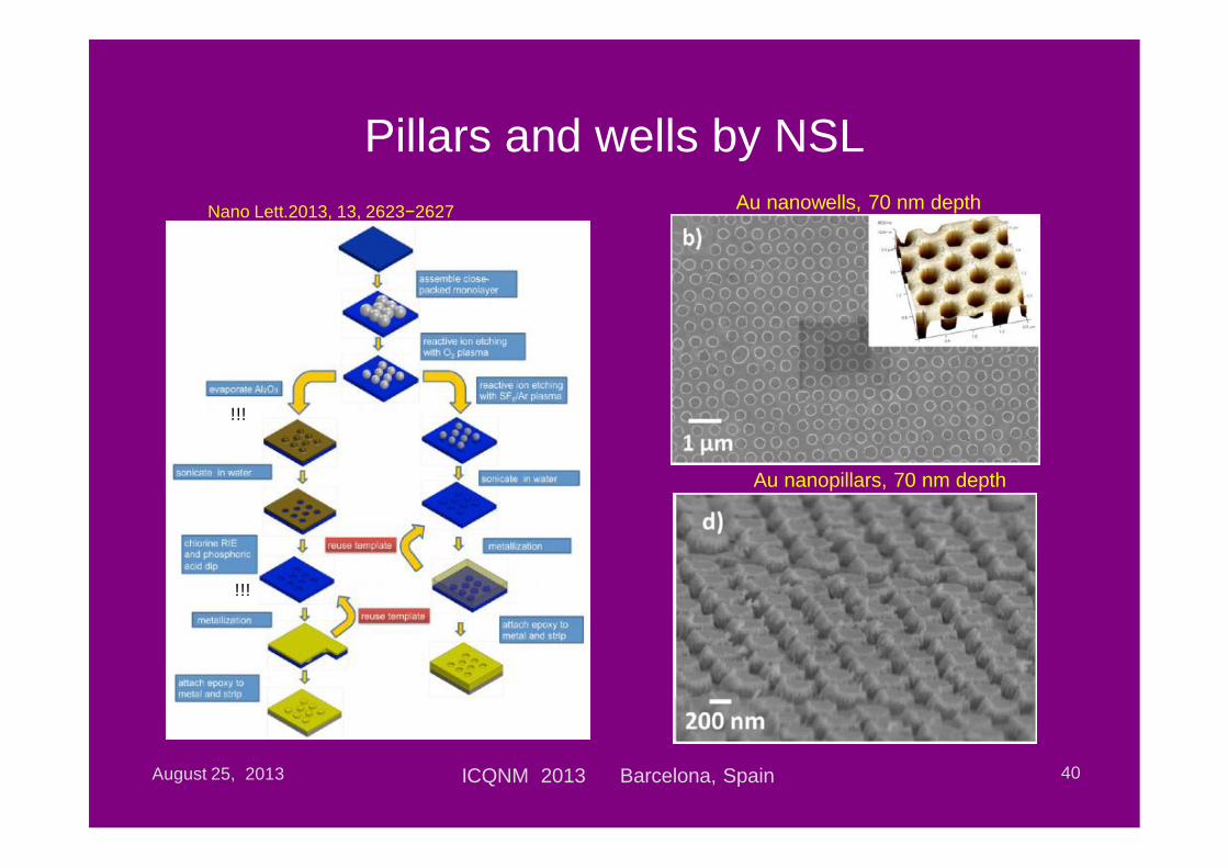
Pillars and wells by NSL
August 25, 2013 ICQNM 2013 Barcelona, Spain 40
Nano Lett.2013, 13, 2623 2627 Au nanowells, 70 nm depth
Au nanopillars, 70 nm depth
!!!
!!!
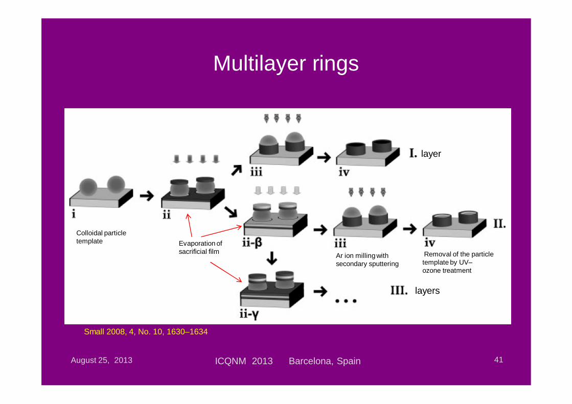
Multilayer rings
August 25, 2013 ICQNM 2013 Barcelona, Spain 41
Small 2008, 4, No. 10, 1630–1634
Colloidal particletemplate Evaporation of
sacri cial lm Ar ion milling with secondary sputtering
Removal of the particle template by UV–ozone treatment
layer
layers
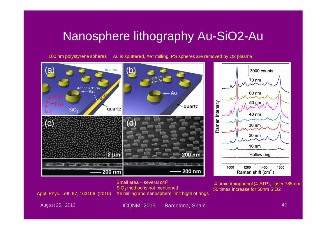
Nanosphere lithography Au-SiO2-Au
August 25, 2013 ICQNM 2013 Barcelona, Spain 42
Appl. Phys. Lett. 97, 163106 (2010)
10-70 nm
100 nm polystyrene spheres
dia 130 × 30 nm
Au is sputtered, Xe+ milling, PS spheres are removed by O2 plasma
4-aminothiophenol (4-ATP), laser 785 nm,50 times increase for 50nm SiO2
Small area – several cm2
SiO2 method is not mentionedXe milling and nanosphere limit higth of rings
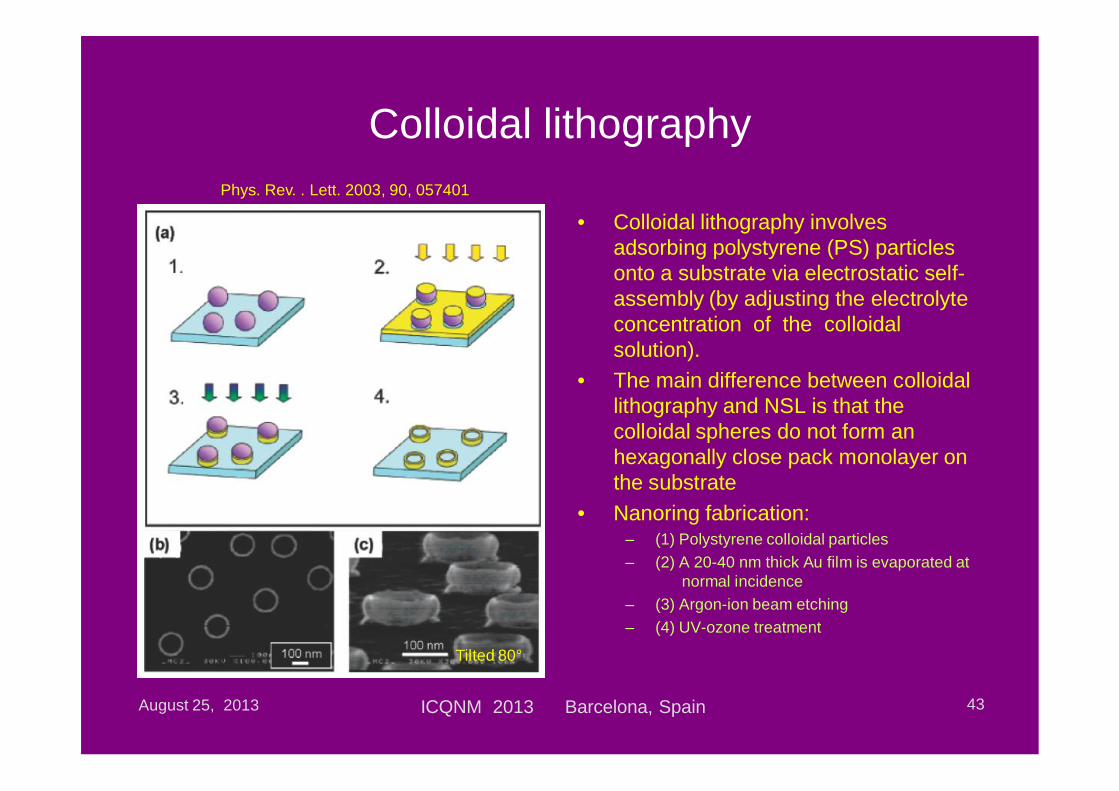
Colloidal lithography
• Colloidal lithography involves adsorbing polystyrene (PS) particles onto a substrate via electrostatic self-assembly (by adjusting the electrolyte concentration of the colloidal solution).
• The main difference between colloidal lithography and NSL is that the colloidal spheres do not form an hexagonally close pack monolayer on the substrate
• Nanoring fabrication:– (1) Polystyrene colloidal particles– (2) A 20-40 nm thick Au film is evaporated at
normal incidence– (3) Argon-ion beam etching– (4) UV-ozone treatment
August 25, 2013 ICQNM 2013 Barcelona, Spain 43
Tilted 80°
Phys. Rev. . Lett. 2003, 90, 057401
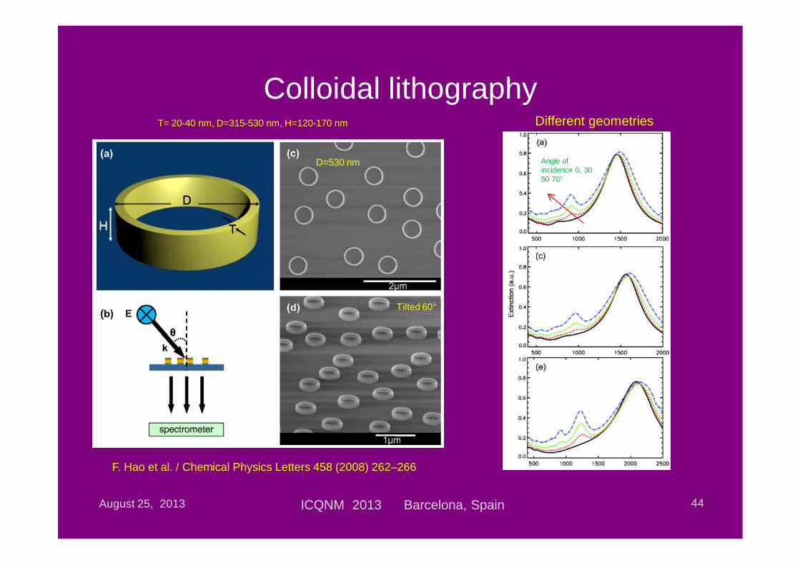
Colloidal lithography
August 25, 2013 ICQNM 2013 Barcelona, Spain 44
Different geometries
Angle of incidence 0, 30 50 70°
F. Hao et al. / Chemical Physics Letters 458 (2008) 262–266
T= 20-40 nm, D=315-530 nm, H=120-170 nm
Tilted 60°
D=530 nm

Arrays of nanopores containingplasmonic particles
August 25, 2013 ICQNM 2013 Barcelona, Spain 45
Nanotechnology 23 (2012) 415304 (7pp)
Colloidal litho
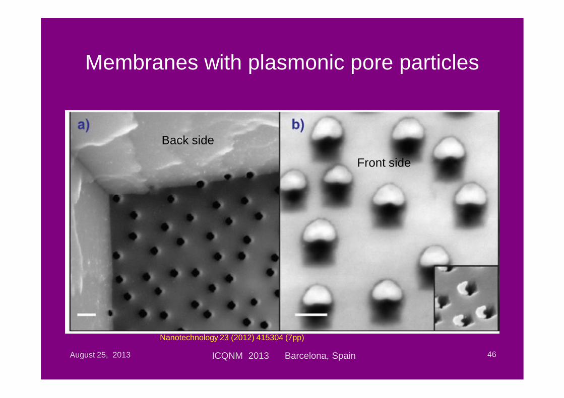
Membranes with plasmonic pore particles
August 25, 2013 ICQNM 2013 Barcelona, Spain 46
Back side
Front side
Nanotechnology 23 (2012) 415304 (7pp)
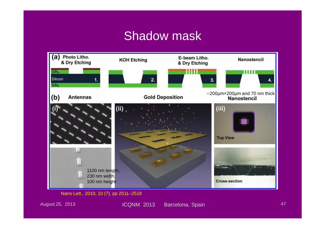
Shadow mask
August 25, 2013 ICQNM 2013 Barcelona, Spain 47
1100 nm length,230 nm width,100 nm height
200µm×200µm and 70 nm thick
Nano Lett., 2010, 10 (7), pp 2511–2518
Shadow mask
• Contact gap - 15% size enlargement, rounded corners, transition area
• Reusing for multiple times• Any substrate material• Several masks can be used consequently• Several deposition angles for controllable
pattern shifting• Alignment problems for multilayers
August 25, 2013 ICQNM 2013 Barcelona, Spain 48

Template stripping, ultrasmooth surface
August 25, 2013 ICQNM 2013 Barcelona, Spain 49
Prashant Nagpal et al., Science, 325, 594 (2009)
7 pairs Ag 30 nm / Al2O3 15nm
Holes 265 nm, Ag 30 nmAg was deposited on Si with pits (NSL)
Ag, 240 nm

Template stripping
• Small samples, i.e. limited area• Inclined walls, already vertical sidewals create
problem for stripping• Limited size, does not work below 100 nm• Smooth surface• Template can be used several times
August 25, 2013 ICQNM 2013 Barcelona, Spain 50
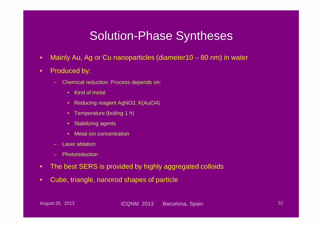
Solution-Phase Syntheses• Mainly Au, Ag or Cu nanoparticles (diameter10 – 80 nm) in water
• Produced by:– Chemical reduction. Process depends on:
• Kind of metal
• Reducing reagent AgNO3, K(AuCl4)
• Temperature (boiling 1 h)
• Stabilizing agents
• Metal ion concentration
– Laser ablation
– Photoreduction
• The best SERS is provided by highly aggregated colloids
• Cube, triangle, nanorod shapes of particle
August 25, 2013 ICQNM 2013 Barcelona, Spain 51
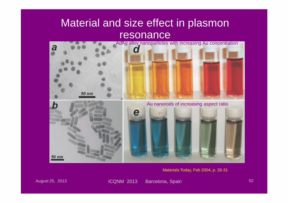
Material and size effect in plasmon resonance
August 25, 2013 ICQNM 2013 Barcelona, Spain 52
Materials Today, Feb 2004, p. 26-31
AuAg alloy nanoparticles with increasing Au concentration
Au nanorods of increasing aspect ratio

Solution-Phase Syntheses• Bottom-up solution-phase synthesis is a versatile approach to
forming NPs that allows control over their size, shape, composition, and structure (e.g., solid or shell).
• Generally involves the reduction of metal salts in a solution containing an appropriate stabilizer to control the growth and suppress the aggregation of the NPs.
• Reduction of the metal salt can be carried out electrochemically, photochemically, sonochemically, or using chemical reductants such as citrate, hydrides, alcohols, hydrogen, hydroxylamine, or hydrazine.
• These particles have facets and should be more correctly called ‘quasi-spheres’
August 25, 2013 ICQNM 2013 Barcelona, Spain 53

Colloids images
August 25, 2013 ICQNM 2013 Barcelona, Spain 54
R.F. Aroca et al. / Advances in Colloid and Interface Science 116 (2005) 45–61
TEM of Ag citrate colloidmax= 406 nm
TEM of Au borohydride colloid,Au particles 20-70 nm,
max= 535 nm
TEM of Au nanorods,max= 525 nm and 885 nm
TEM of Au nanosquares
AFM of Au nanospheres embeddedin film of biopoymer chitosan
(inert organic matrix)
AFM of Ag nanowiresin dendrimer matrix

SPR of colloids
August 25, 2013 ICQNM 2013 Barcelona, Spain 55
R.F. Aroca et al. / Advances in Colloid and Interface Science 116 (2005) 45–61
Partical surface charge determs stability, adsorbivity, electrokinetic properties
Observed effects are due toparticle size, concentration,aspect ratio.
Abs
orpt
ion
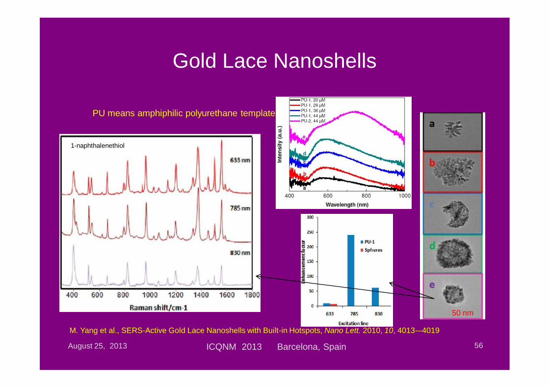
Gold Lace Nanoshells
August 25, 2013 ICQNM 2013 Barcelona, Spain 56
50 nm
M. Yang et al., SERS-Active Gold Lace Nanoshells with Built-in Hotspots, Nano Lett. 2010, 10, 4013-–4019
1-naphthalenethiol
PU means amphiphilic polyurethane template
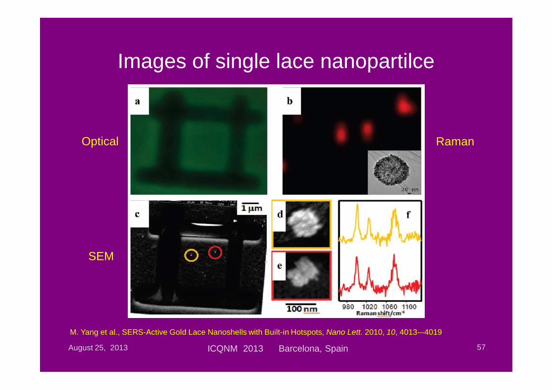
Images of single lace nanopartilce
August 25, 2013 ICQNM 2013 Barcelona, Spain 57
M. Yang et al., SERS-Active Gold Lace Nanoshells with Built-in Hotspots, Nano Lett. 2010, 10, 4013-–4019
Optical Raman
SEM
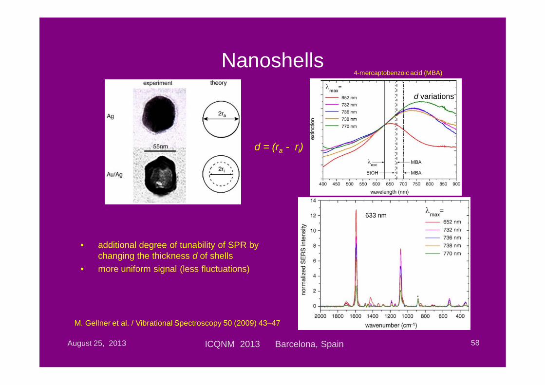
Nanoshells
• additional degree of tunability of SPR by changing the thickness d of shells
• more uniform signal (less fluctuations)
August 25, 2013 ICQNM 2013 Barcelona, Spain 58
M. Gellner et al. / Vibrational Spectroscopy 50 (2009) 43–47
d = (ra - ri)
d variations
4-mercaptobenzoic acid (MBA)
633 nm
Metal nanostructured films
Prepared by different methods:electrochemistry methodsphysical vapor deposition (PVD) and annealingoblique angle depositionglanced angle deposition (GLAD)
• Applicability to any substrate• High purity• Structure can be controlled by deposition rate (0.5
A/s), substrate roughness, temperature, mass thickness (6 nm), post annealing
• Cold-deposited (-100 ºC) Ag (pore, voids, cavities)
August 25, 2013 ICQNM 2013 Barcelona, Spain 59
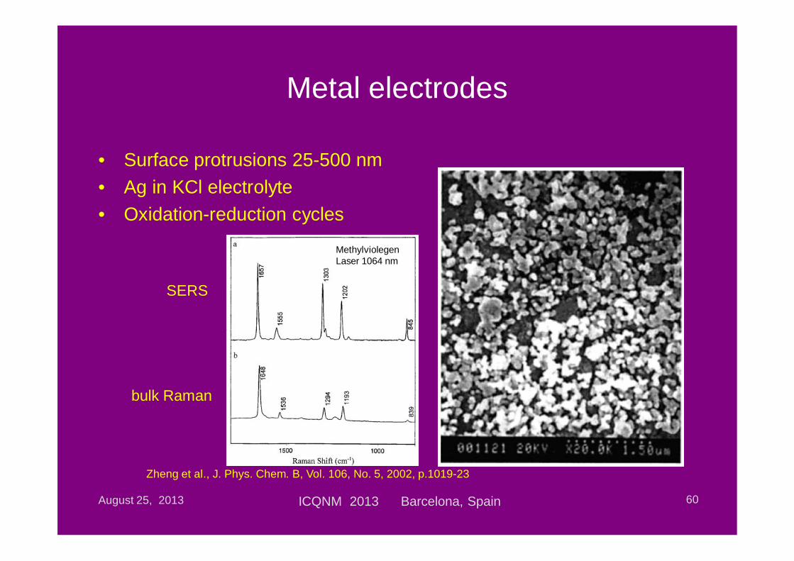
Metal electrodes
• Surface protrusions 25-500 nm• Ag in KCl electrolyte• Oxidation-reduction cycles
August 25, 2013 ICQNM 2013 Barcelona, Spain 60
MethylviolegenLaser 1064 nm
bulk Raman
SERS
Zheng et al., J. Phys. Chem. B, Vol. 106, No. 5, 2002, p.1019-23
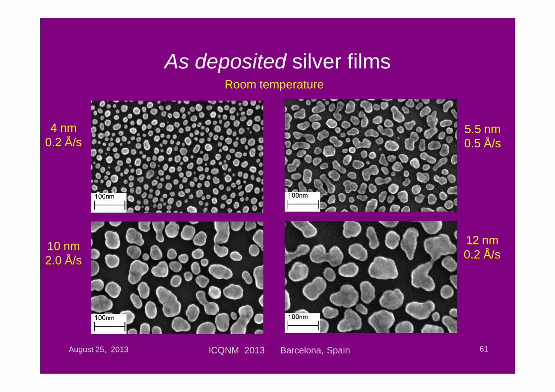
As deposited silver films
August 25, 2013 ICQNM 2013 Barcelona, Spain 61
4 nm0.2 Å/s
5.5 nm0.5 Å/s
10 nm2.0 Å/s
12 nm0.2 Å/s
Room temperature
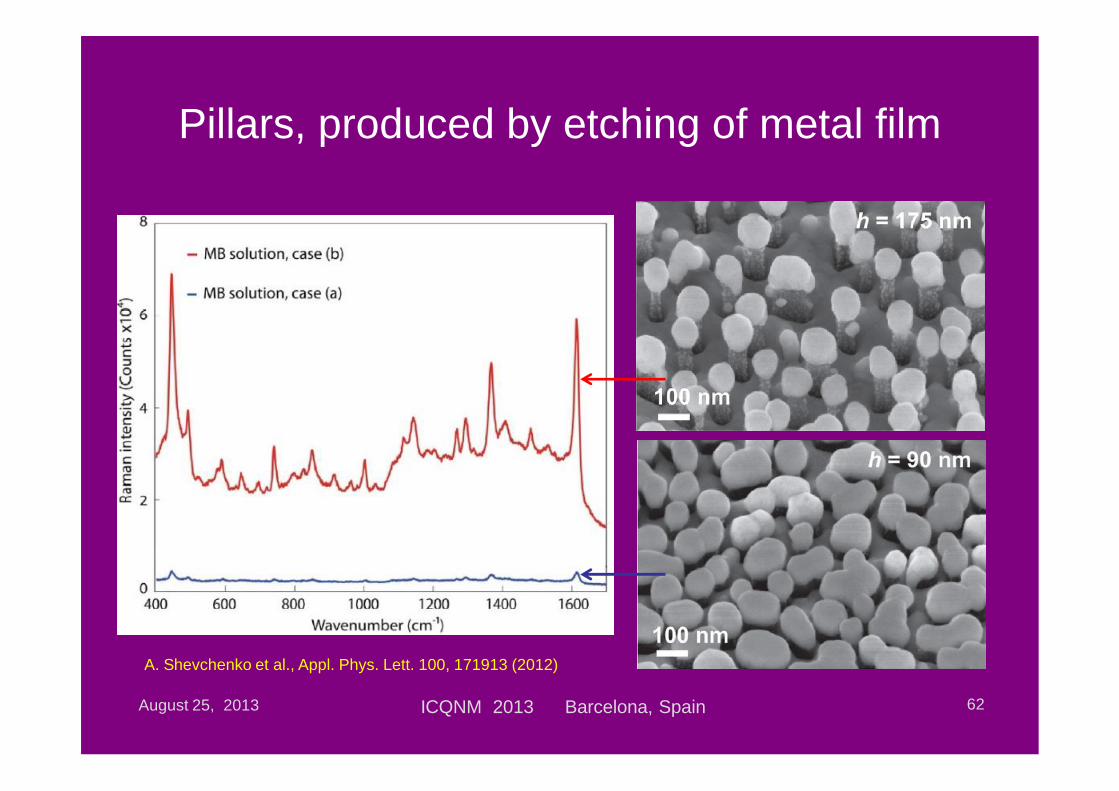
Pillars, produced by etching of metal film
August 25, 2013 ICQNM 2013 Barcelona, Spain 62
A. Shevchenko et al., Appl. Phys. Lett. 100, 171913 (2012)

Fine structure of deposited metal film
August 25, 2013 ICQNM 2013 Barcelona, Spain 63
A. Shevchenko et al., Appl. Phys. Lett. 100, 171913 (2012)
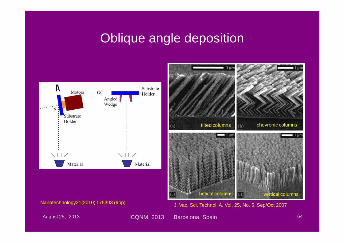
Oblique angle deposition
August 25, 2013 ICQNM 2013 Barcelona, Spain 64
Nanotechnology21(2010) 175303 (9pp) J. Vac. Sci. Technol. A, Vol. 25, No. 5, Sep/Oct 2007
tilted columns chevronic columns
helical columns vertical columns
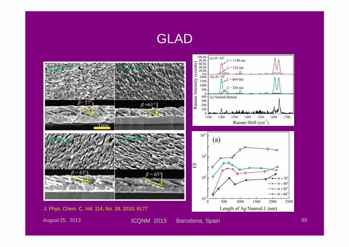
GLAD
August 25, 2013 ICQNM 2013 Barcelona, Spain 65
J. Phys. Chem. C, Vol. 114, No. 18, 2010, 8177

GLAD features
• Wafer scale, i.e. the whole wafer can be covered by the nanostructures
• No adhesion layer – problems during further processing
• Limited variations of morphology
August 25, 2013 ICQNM 2013 Barcelona, Spain 66
August 26, 2013 ICQNM 2013 Barcelona, Spain 67
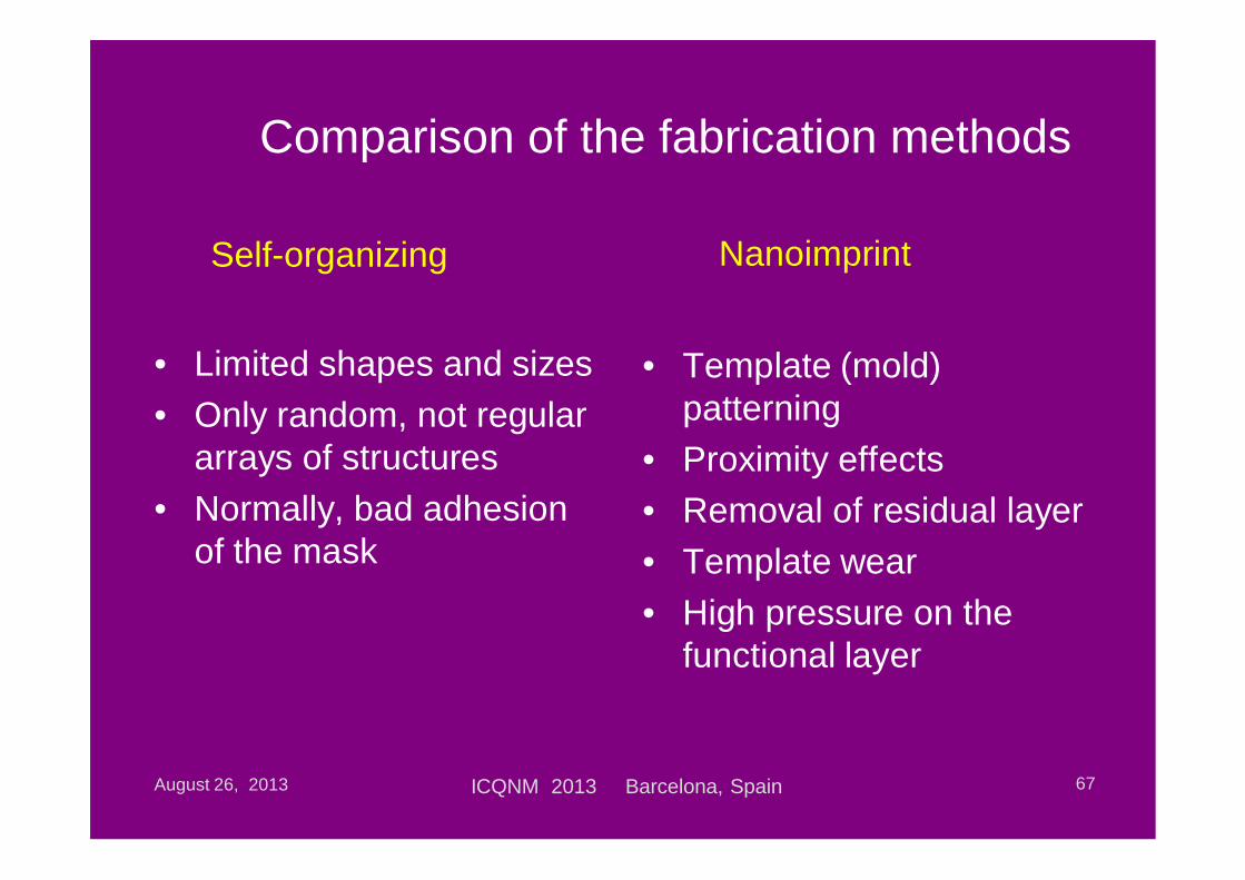
Comparison of the fabrication methods
• Limited shapes and sizes• Only random, not regular
arrays of structures• Normally, bad adhesion
of the mask
• Template (mold) patterning
• Proximity effects• Removal of residual layer• Template wear• High pressure on the
functional layer
Self-organizing Nanoimprint

Summary
• Plasmonics is rapidly development area of nanophotonics. It promises attractive applications in many fields of science and engineering
• There is no ideal method to fabricate low cost plasmonic devices in reproducible way
• Every plasmonic application has own, most suitable fabrication tehnique and vice versa every nanotechnology method has limited application
August 25, 2013 ICQNM 2013 Barcelona, Spain 68
Plasmonic future
• Application of new plasmonic materials (graphene, semiconductors). It helps to reduce the losses inherent in the interaction of light with metal, but only in visible range
• Development of the new fabrication techniques
August 25, 2013 ICQNM 2013 Barcelona, Spain 69