
Plasmon-phonon interactions in topological …Plasmon-phonon interactions in topological insulator...
9
Plasmon-phonon interactions in topological insulator rings M. Autore, 1 F. D’Apuzzo, 2 A. Di Gaspare, 3 V. Giliberti, 4 O. Limaj, 1 P. Roy, 5 M. Brahlek, 6 N. Koirala, 6 S. Oh, 6 F. J. García de Abajo*, 7 and S. Lupi* 8 1 INFN and Dipartimento di Fisica, Università di Roma "La Sapienza", Piazzale A. Moro 2, I-00185 Roma, Italy 2 Istituto Italiano di Tecnologia and Dipartimento di Fisica, Università di Roma La Sapienza, Piazzale Aldo Moro 2, I-00185 Roma, Italy 3 CNR-IFN and LNF-INFN, Via E. Fermi 40, 00044 Frascati, Italy 4 CNR-IFN and Dipartimento di Fisica, Università di Roma "La Sapienza", Piazzale A. Moro 2, I-00185 Roma, Italy 5 Synchrotron Soleil, L’Orme des Merisiers, Saint Aubin, BP 48, 91192 Gif-sur-Yvette, France 6 Department of Physics and Astronomy Rutgers, The State University of New Jersey 136 Frelinghuysen Road Piscataway, NJ 08854-8019 USA 7 ICFO-Institut de Ciencies Fotoniques, Mediterranean Technology Park, 08860 Castelldefels (Barcelona), Spain * 8 INFN, CNR-IOM, and Dipartimento di Fisica, Università di Roma "La Sapienza", Piazzale A. Moro 2, I-00185 Roma, Italy (Dated: September 30, 2018) PACS numbers: 71.30.+h, 78.30.-j, 62.50.+p The great potential of Dirac electrons for plas- monics and photonics has been readily recog- nized after their discovery in graphene, followed by applications to smart optical devices. Dirac carriers are also found in topological insulators (TI) –quantum systems having an insulating gap in the bulk and intrinsic Dirac metallic states at the surface–. Here, we investigate the plas- monic response of ring structures patterned in Bi 2 Se 3 TI films, which we investigate through ter- ahertz (THz) spectroscopy. The rings are ob- served to exhibit a bonding and an antibond- ing plasmon modes, which we tune in frequency by varying their diameter. We develop an an- alytical theory based on the THz conductiv- ity of unpatterned films, which accurately de- scribes the strong plasmon-phonon hybridization and Fano interference experimentally observed as the bonding plasmon is swiped across the promi- neng 2 THz phonon exhibited by this material. This work opens the road for the investigation of plasmons in topological insulators and for their application in tunable THz devices. Plasmons –the collective oscillations of charge carriers in conducting materials– hold great potential for com- bining electronics and photonics at the nanoscale. These excitations can propagate along extended surfaces or they can be localized at so-called hotspots. The engineer- ing of plasmon frequencies and spatial profiles has been mastered in metallic micro- and nanostructures such as nanospheres, nanorods [1], dimers [2, 3], particle arrays [4, 5], and a plethora of more exotic morphologies [6–9]. Plasmon hybridization [10, 11], Fano resonances [12, 13], and electromagnetically induced transparency [14] are among the feats that have been realized and broadly used to understand and design plasmonic devices. The range of applications of plasmon excitations is vast and in- cludes optical sensing [15–18], quantum electrodynamics [19, 20], nonlinar optics [21, 22], photovoltaic technolo- gies [23], and medical diagnosis and treatment [24, 25]. Extensive experimental efforts are currently underway to find materials with improved plasmonic performance, in particular in the mid-infrared and terahertz parts of the electromagnetic spectrum. Examples of such ma- terials are low- [26] and high-Tc superconductors [14], conductive oxides [27], and graphene [28–34]. The lat- ter exhibits a peculiar electronic structure, which en- ables unprecedented levels of electro-optical tunability via chemical or electrostatic doping [35–37]: electrons in graphene behave as massless Dirac fermions charac- terized by a linear dispersion relation and a vanishing density of states at the Fermi energy, so that a few addi- tional charge carriers produce a large shift in the chemical potential. Dirac charge carriers are also found in three- dimensional topological insulator materials –i.e., quan- tum systems characterized by an insulating electronic gap in the bulk, which opening is due to strong spin-orbit in- teraction, and gapless surface states at the edge and in- terface. Surface states in TIs are metallic and chiral, as- sociated with massless Dirac quasi-particles [38–40], and protected from back-scattering by time-reversal symme- try. This means that they cannot be destroyed or gapped by scattering processes, other than magnetic impurities. Furthermore, unlike graphene, TI surface states sponta- neously provide a 2D Dirac-fermion system, segregated from the bulk material without the need of physically im- plementing an atomic monolayer. Since their discovery, TI’s have attracted a growing interest due to their po- tential application in quantum computing [41, 42], THz detectors [43], and spintronic devices [44], and some of these applications could benefit from propagating and localized plasmons sustainted by these materials. Recently, propagating plasmons have been observed in the THz domain in micro-ribbon arrays patterned on Bi 2 Se 3 TI films [45]. The plasmon frequency ν P was found to follow an optical dispersion relation ν P ∝ arXiv:1504.02592v1 [cond-mat.mtrl-sci] 10 Apr 2015
Transcript of Plasmon-phonon interactions in topological …Plasmon-phonon interactions in topological insulator...
Plasmon-phonon interactions in topological insulator rings
M. Autore,1 F. D’Apuzzo,2 A. Di Gaspare,3 V. Giliberti,4 O. Limaj,1 P. Roy,5M. Brahlek,6 N. Koirala,6 S. Oh,6 F. J. García de Abajo*,7 and S. Lupi*8
1INFN and Dipartimento di Fisica, Università di Roma "La Sapienza", Piazzale A. Moro 2, I-00185 Roma, Italy2Istituto Italiano di Tecnologia and Dipartimento di Fisica,
Università di Roma La Sapienza, Piazzale Aldo Moro 2, I-00185 Roma, Italy3CNR-IFN and LNF-INFN, Via E. Fermi 40, 00044 Frascati, Italy
4CNR-IFN and Dipartimento di Fisica, Università di Roma "La Sapienza", Piazzale A. Moro 2, I-00185 Roma, Italy5Synchrotron Soleil, L’Orme des Merisiers, Saint Aubin, BP 48, 91192 Gif-sur-Yvette, France
6Department of Physics and Astronomy Rutgers,The State University of New Jersey 136 Frelinghuysen Road Piscataway, NJ 08854-8019 USA
7ICFO-Institut de Ciencies Fotoniques, Mediterranean Technology Park, 08860 Castelldefels (Barcelona), Spain∗
8INFN, CNR-IOM, and Dipartimento di Fisica, Università di Roma "La Sapienza", Piazzale A. Moro 2, I-00185 Roma, Italy(Dated: September 30, 2018)
PACS numbers: 71.30.+h, 78.30.-j, 62.50.+p
The great potential of Dirac electrons for plas-monics and photonics has been readily recog-nized after their discovery in graphene, followedby applications to smart optical devices. Diraccarriers are also found in topological insulators(TI) –quantum systems having an insulating gapin the bulk and intrinsic Dirac metallic statesat the surface–. Here, we investigate the plas-monic response of ring structures patterned inBi2Se3 TI films, which we investigate through ter-ahertz (THz) spectroscopy. The rings are ob-served to exhibit a bonding and an antibond-ing plasmon modes, which we tune in frequencyby varying their diameter. We develop an an-alytical theory based on the THz conductiv-ity of unpatterned films, which accurately de-scribes the strong plasmon-phonon hybridizationand Fano interference experimentally observed asthe bonding plasmon is swiped across the promi-neng 2THz phonon exhibited by this material.This work opens the road for the investigation ofplasmons in topological insulators and for theirapplication in tunable THz devices.
Plasmons –the collective oscillations of charge carriersin conducting materials– hold great potential for com-bining electronics and photonics at the nanoscale. Theseexcitations can propagate along extended surfaces or theycan be localized at so-called hotspots. The engineer-ing of plasmon frequencies and spatial profiles has beenmastered in metallic micro- and nanostructures such asnanospheres, nanorods [1], dimers [2, 3], particle arrays[4, 5], and a plethora of more exotic morphologies [6–9].Plasmon hybridization [10, 11], Fano resonances [12, 13],and electromagnetically induced transparency [14] areamong the feats that have been realized and broadly usedto understand and design plasmonic devices. The rangeof applications of plasmon excitations is vast and in-cludes optical sensing [15–18], quantum electrodynamics
[19, 20], nonlinar optics [21, 22], photovoltaic technolo-gies [23], and medical diagnosis and treatment [24, 25].Extensive experimental efforts are currently underway
to find materials with improved plasmonic performance,in particular in the mid-infrared and terahertz parts ofthe electromagnetic spectrum. Examples of such ma-terials are low- [26] and high-Tc superconductors [14],conductive oxides [27], and graphene [28–34]. The lat-ter exhibits a peculiar electronic structure, which en-ables unprecedented levels of electro-optical tunabilityvia chemical or electrostatic doping [35–37]: electronsin graphene behave as massless Dirac fermions charac-terized by a linear dispersion relation and a vanishingdensity of states at the Fermi energy, so that a few addi-tional charge carriers produce a large shift in the chemicalpotential. Dirac charge carriers are also found in three-dimensional topological insulator materials –i.e., quan-tum systems characterized by an insulating electronic gapin the bulk, which opening is due to strong spin-orbit in-teraction, and gapless surface states at the edge and in-terface. Surface states in TIs are metallic and chiral, as-sociated with massless Dirac quasi-particles [38–40], andprotected from back-scattering by time-reversal symme-try. This means that they cannot be destroyed or gappedby scattering processes, other than magnetic impurities.Furthermore, unlike graphene, TI surface states sponta-neously provide a 2D Dirac-fermion system, segregatedfrom the bulk material without the need of physically im-plementing an atomic monolayer. Since their discovery,TI’s have attracted a growing interest due to their po-tential application in quantum computing [41, 42], THzdetectors [43], and spintronic devices [44], and some ofthese applications could benefit from propagating andlocalized plasmons sustainted by these materials.Recently, propagating plasmons have been observed
in the THz domain in micro-ribbon arrays patternedon Bi2Se3 TI films [45]. The plasmon frequency νP
was found to follow an optical dispersion relation νP ∝
arX
iv:1
504.
0259
2v1
[co
nd-m
at.m
trl-
sci]
10
Apr
201
5
2
1/√W , where W is the ribbon width, characteristic of
2D metal systems and in excellent agreement with thatpredicted for Dirac plasmons. [46, 47] However, despitetheir potential for novel applications, neither localizedplasmons nor their hybridization and coupling have yetbeen explored in TI micro and nano structures. In thisLetter, we reveal the behavior of localized plasmons intopological insulator rings (TIRs), with a particular fo-cus on their dependence on size and temperature, as wellas on their hybridization with a Bi2Se3 optical phononlocated at 2 THz. We demonstrate geometrical tuning ofthe TIR plasmons and the resulting hybridization thatexhibit a strong temperature dependence as observed intransmission spectra. This study indicates that TIRshold a great potential for applications in thermally con-trolled THz devices.
RESULTS
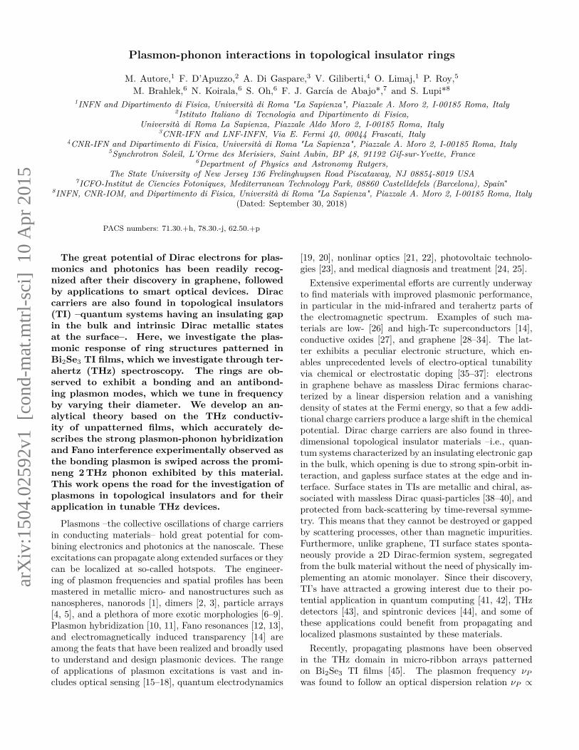
Five films of Bi2Se3 (thickness h = 60 quintuple lay-ers ' 60nm) were grown by molecular beam epitaxy on0.5mm thick sapphire (Al2O3) substrates [48, 49]. Thefilms were characterized through resistivity and Hall mea-surements [48, 49] (see Methods for details) indicatingthe presence of a 2D gas of Dirac electrons with a surfacedensity nD = 3±1×1013 cm−2. One of the films was keptas grown to serve as a reference, while the other four werepatterned by electron-beam lithography and reactive-ionetching to form periodic hexagonal arrays of rings withdifferent sizes. The outer (D) and inner (d) ring diam-eters were chosen to have a similar disk-to-hole aspectratio (D/d ' 3), while the lattice period a was taken tobe approximately 4 times the inner diameter (a/d = 4)in all samples. Fig. 1a shows a scanning electron mi-croscope (SEM) image of the D = 15µm patterned film,whereas Fig. 1c presents optical microscope images ofthe different arrays.
The transmittance T (ν) of the five films was measuredin the terahertz domain using a Fourier-transform in-terferometer at temperatures held in the range of 10 to300 K in the AILES beamline at the synchrotron Soleil[50, 51]. Each transmittance has been normalized to thatof the sapphire substrate collected at the same temper-ature. The corresponding extinction coefficient (Extinc-tion = 1-Transmittance) is plotted in Fig. 1b for theas-grown sample and in Fig. 1d for the patterned filmsat 10K (blue curves), 100K (green curves), and 300K(red curves).
The extinction spectra in Fig. 1d exhibit several peaksshifting to higher frequency (blueshifting) as the ringsize is decreased. These features are accompanied bya prominent dip-peak structure at a nearly constant fre-quency ∼ 2 THz, independent of ring size. Additionally,a strong dependence on temperature is observed, includ-ing a reduction in the contrast of the observed dip-peak
structure, as well as a broad increase in the extinction athigher frequencies.Quantitative insight into the origin of the observed
spectra is obtained from theoretical simulations per-formed starting from the dielectric properties of the un-patterned film (see Methods for details). Since the thick-ness of the Bi2Se3 film is small compared with both thelateral size of the rings and the terahertz wavelengths, wecan model them through a 2D surface conductivity (seeMethods). Before analyzing the effects of nanostructur-ing, it is worth looking into the properties of this conduc-tivity, as extracted from extinction measurements for theunpatterned film of the same thickness (Fig. 1b). Theextinction of this film exhibits a phonon peak (α mode)at 1.85 THz, already observed in Bi2Se3 single crystals[52]. This phonon is superimposed on an electronic back-ground that decreases monotonically with frequency andthat is associated with Dirac surface states [53]. Theresulting conductivity is then modeled through two con-tributions: a Lorentzian to represent the α phonon anda Drude term accounting for the response of the surfaceDirac electron gas (see Eq. 2 in Methods). The for-mer is expected to depend linearly on the film thickness,as the optical phonons are spatially localized and con-tribute all over the volume of the material. In contrast,the Drude term is independent of thickness but dependson the combined surface electron densities on both sidesof the film. This metallic contribution is also stronglydependent on temperature (see Fig. 1b), presumably asa result of thermal smearing of the surface electron gas(notice that KBT/~ = 2.1 THz at T = 100 K).By fitting the spectra of the homogeneous film (see
Tab.I in Methods), we can parametrize the TI film con-ductivity and use it to perform classical electromagneticsimulations as discussed in the Methods section. Calcu-lations are carried out for all three temperatures underconsideration and the resulting theoretical spectra verywell reproduce both the experimental extinction of theunpatterned film (Fig. 1b), and those of the patternedones (Fig. 1e). In particular for the ring-arrays (Fig. 1e),analytical calculations reproduce the extinction shape,the main features of the temperature dependence notedabove, as well as the general trend of the evolution ofspectral maxima and minima with ring size.If we artificially switch off the α phonon contribu-
tion from the film conductivity (i.e., by removing theLorentzian term in Eq. 2 of Methods), the extinctionspectra are simplified and consist of two dominant max-ima that evolve towards higher frequencies for smallerrings (Fig. 1e, dashed curves). Because only the Drudeterm contributes to the conductivity in this case, theobserved features can be undoubtedly assigned to plas-monic excitations. Closer examination of the origin ofthese features (see Methods) reveals that they are thebonding (at low energy) and antibonding (at higher en-ergy) ring plasmons. Moving back to the full simulation
3
D = 15 µm, d = 5 µm
D = 8 µm, d = 2.5 µm
D = 5 µm, d = 1.5 µm
D = 3 µm, d = 1 µm
a b
c
d
1.0
0.5
0.0
Ex
tin
ctio
n
6420
T = 10 K 100 K 300 K
ν (THz)
ν (THz)
0.4
0.2
0.0
T = 10 K 100 K 300 K
0.4
0.2
0.0
0.4
0.2
0.0
0.4
0.2
0.06420
0.4
0.2
0.0
0.4
0.2
0.0
0.4
0.2
0.0
0.4
0.2
0.06420
ν (THz)
Ex
tin
ctio
n
e experiment theory
Ex
tin
ctio
n
FIG. 1: Geometrical tuning of the plasmonic response of topological insulator rings (TIRs). (a) Detailed SEMimage of a Bi2Se3 TIR having an outer (inner) diameter D= 15 (d = 5) µm. (b) Extinction (= 1−Transmittance) spectraof unpatterned Bi2Se3 film (60 nm thickness) at different temperatures. Dashed lines represent calculated extinctions for theunpatterned film (see text and Methods). (c-e) Optical images (c), measured extinction (d), and calculated extinction (e) ofBi2Se3 ring arrays for different ring sizes, as specified in (c) (see labels with the values of D and d, respectively). The arraylattice period is 4d and the D/d aspect ratio is close to 3 in all samples, whereas the ring size decreases from the top to thebottom panel. The transmittance is normalized to that of the sapphire substrate measured at the same temperature. Thecalculations of (e) are performed with (solid curves) and without (broken curves) the inclusion of the TI α phonon.
including phonons (Fig. 1e, solid curves), we still iden-tify the presence of both types of plasmons, although thebroad bonding mode is now strongly perturbed by the rel-atively narrow optical phonon. The resulting plasmon-phonon interaction gives rise to characteristic dip-peakline shapes that are reminescent of the Fano interferenceobserved in other plasmonic systems [12, 13, 45, 54].
For the smallest ring under consideration (D = 3µm),a slight disagreement is observed at high frequency be-tween experimental data and theory (cf. Fig. 1d,e,bottom panels). In particular, the experimental anti-bonding absorption peak (above the α phonon), appearsto be broader than the calculated one. This could be as-cribed to unaccounted decay channels other than ohmic
4
(single-particle) scattering, which is the only one consid-ered in the calculation and common to both plasmons.In this respect, fabrication defects cannot be ruled out,as they are expected to have stronger influence on thehigh-frequency (antibonding) plasmon mode.
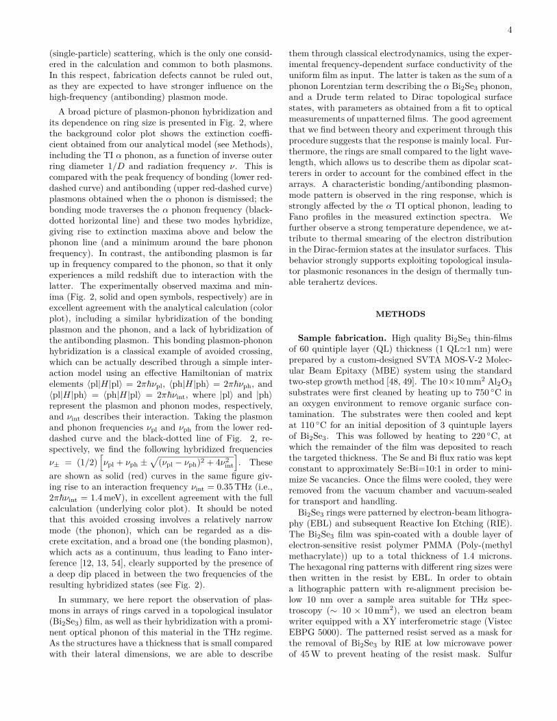
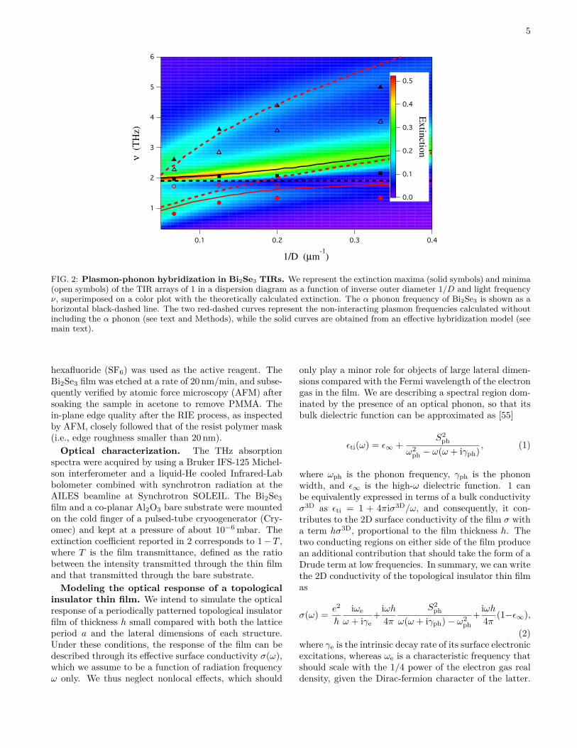
A broad picture of plasmon-phonon hybridization andits dependence on ring size is presented in Fig. 2, wherethe background color plot shows the extinction coeffi-cient obtained from our analytical model (see Methods),including the TI α phonon, as a function of inverse outerring diameter 1/D and radiation frequency ν. This iscompared with the peak frequency of bonding (lower red-dashed curve) and antibonding (upper red-dashed curve)plasmons obtained when the α phonon is dismissed; thebonding mode traverses the α phonon frequency (black-dotted horizontal line) and these two modes hybridize,giving rise to extinction maxima above and below thephonon line (and a minimum around the bare phononfrequency). In contrast, the antibonding plasmon is farup in frequency compared to the phonon, so that it onlyexperiences a mild redshift due to interaction with thelatter. The experimentally observed maxima and min-ima (Fig. 2, solid and open symbols, respectively) are inexcellent agreement with the analytical calculation (colorplot), including a similar hybridization of the bondingplasmon and the phonon, and a lack of hybridization ofthe antibonding plasmon. This bonding plasmon-phononhybridization is a classical example of avoided crossing,which can be actually described through a simple inter-action model using an effective Hamiltonian of matrixelements 〈pl|H|pl〉 = 2π~νpl, 〈ph|H|ph〉 = 2π~νph, and〈pl|H|ph〉 = 〈ph|H|pl〉 = 2π~νint, where |pl〉 and |ph〉represent the plasmon and phonon modes, respectively,and νint describes their interaction. Taking the plasmonand phonon frequencies νpl and νph from the lower red-dashed curve and the black-dotted line of Fig. 2, re-spectively, we find the following hybridized frequenciesν± = (1/2)
[νpl + νph ±
√(νpl − νph)2 + 4ν2
int
]. These
are shown as solid (red) curves in the same figure giv-ing rise to an interaction frequency νint = 0.35THz (i.e.,2π~νint = 1.4meV), in excellent agreement with the fullcalculation (underlying color plot). It should be notedthat this avoided crossing involves a relatively narrowmode (the phonon), which can be regarded as a dis-crete excitation, and a broad one (the bonding plasmon),which acts as a continuum, thus leading to Fano inter-ference [12, 13, 54], clearly supported by the presence ofa deep dip placed in between the two frequencies of theresulting hybridized states (see Fig. 2).
In summary, we here report the observation of plas-mons in arrays of rings carved in a topological insulator(Bi2Se3) film, as well as their hybridization with a promi-nent optical phonon of this material in the THz regime.As the structures have a thickness that is small comparedwith their lateral dimensions, we are able to describe
them through classical electrodynamics, using the exper-imental frequency-dependent surface conductivity of theuniform film as input. The latter is taken as the sum of aphonon Lorentzian term describing the α Bi2Se3 phonon,and a Drude term related to Dirac topological surfacestates, with parameters as obtained from a fit to opticalmeasurements of unpatterned films. The good agreementthat we find between theory and experiment through thisprocedure suggests that the response is mainly local. Fur-thermore, the rings are small compared to the light wave-length, which allows us to describe them as dipolar scat-terers in order to account for the combined effect in thearrays. A characteristic bonding/antibonding plasmon-mode pattern is observed in the ring response, which isstrongly affected by the α TI optical phonon, leading toFano profiles in the measured extinction spectra. Wefurther observe a strong temperature dependence, we at-tribute to thermal smearing of the electron distributionin the Dirac-fermion states at the insulator surfaces. Thisbehavior strongly supports exploiting topological insula-tor plasmonic resonances in the design of thermally tun-able terahertz devices.
METHODS
Sample fabrication. High quality Bi2Se3 thin-filmsof 60 quintiple layer (QL) thickness (1 QL'1 nm) wereprepared by a custom-designed SVTA MOS-V-2 Molec-ular Beam Epitaxy (MBE) system using the standardtwo-step growth method [48, 49]. The 10×10mm2 Al2O3substrates were first cleaned by heating up to 750 C inan oxygen environment to remove organic surface con-tamination. The substrates were then cooled and keptat 110 C for an initial deposition of 3 quintuple layersof Bi2Se3. This was followed by heating to 220 C, atwhich the remainder of the film was deposited to reachthe targeted thickness. The Se and Bi flux ratio was keptconstant to approximately Se:Bi=10:1 in order to mini-mize Se vacancies. Once the films were cooled, they wereremoved from the vacuum chamber and vacuum-sealedfor transport and handling.Bi2Se3 rings were patterned by electron-beam lithogra-
phy (EBL) and subsequent Reactive Ion Etching (RIE).The Bi2Se3 film was spin-coated with a double layer ofelectron-sensitive resist polymer PMMA (Poly-(methylmethacrylate)) up to a total thickness of 1.4 microns.The hexagonal ring patterns with different ring sizes werethen written in the resist by EBL. In order to obtaina lithographic pattern with re-alignment precision be-low 10 nm over a sample area suitable for THz spec-troscopy (∼ 10 × 10mm2), we used an electron beamwriter equipped with a XY interferometric stage (VistecEBPG 5000). The patterned resist served as a mask forthe removal of Bi2Se3 by RIE at low microwave powerof 45W to prevent heating of the resist mask. Sulfur
5
6
5
4
3
2
1
ν
(TH
z)
0.40.30.20.1
1/D (µm-1
)
0.5
0.4
0.3
0.2
0.1
0.0
Extin
ctio
n
FIG. 2: Plasmon-phonon hybridization in Bi2Se3 TIRs. We represent the extinction maxima (solid symbols) and minima(open symbols) of the TIR arrays of 1 in a dispersion diagram as a function of inverse outer diameter 1/D and light frequencyν, superimposed on a color plot with the theoretically calculated extinction. The α phonon frequency of Bi2Se3 is shown as ahorizontal black-dashed line. The two red-dashed curves represent the non-interacting plasmon frequencies calculated withoutincluding the α phonon (see text and Methods), while the solid curves are obtained from an effective hybridization model (seemain text).
hexafluoride (SF6) was used as the active reagent. TheBi2Se3 film was etched at a rate of 20 nm/min, and subse-quently verified by atomic force microscopy (AFM) aftersoaking the sample in acetone to remove PMMA. Thein-plane edge quality after the RIE process, as inspectedby AFM, closely followed that of the resist polymer mask(i.e., edge roughness smaller than 20 nm).Optical characterization. The THz absorption
spectra were acquired by using a Bruker IFS-125 Michel-son interferometer and a liquid-He cooled Infrared-Labbolometer combined with synchrotron radiation at theAILES beamline at Synchrotron SOLEIL. The Bi2Se3film and a co-planar Al2O3 bare substrate were mountedon the cold finger of a pulsed-tube cryoogenerator (Cry-omec) and kept at a pressure of about 10−6 mbar. Theextinction coefficient reported in 2 corresponds to 1− T ,where T is the film transmittance, defined as the ratiobetween the intensity transmitted through the thin filmand that transmitted through the bare substrate.Modeling the optical response of a topological
insulator thin film. We intend to simulate the opticalresponse of a periodically patterned topological insulatorfilm of thickness h small compared with both the latticeperiod a and the lateral dimensions of each structure.Under these conditions, the response of the film can bedescribed through its effective surface conductivity σ(ω),which we assume to be a function of radiation frequencyω only. We thus neglect nonlocal effects, which should
only play a minor role for objects of large lateral dimen-sions compared with the Fermi wavelength of the electrongas in the film. We are describing a spectral region dom-inated by the presence of an optical phonon, so that itsbulk dielectric function can be approximated as [55]
εti(ω) = ε∞ +S2
ph
ω2ph − ω(ω + iγph) , (1)
where ωph is the phonon frequency, γph is the phononwidth, and ε∞ is the high-ω dielectric function. 1 canbe equivalently expressed in terms of a bulk conductivityσ3D as εti = 1 + 4πiσ3D/ω, and consequently, it con-tributes to the 2D surface conductivity of the film σ witha term hσ3D, proportional to the film thickness h. Thetwo conducting regions on either side of the film producean additional contribution that should take the form of aDrude term at low frequencies. In summary, we can writethe 2D conductivity of the topological insulator thin filmas
σ(ω) = e2
~iωe
ω + iγe+iωh
4πS2
ph
ω(ω + iγph)− ω2ph
+iωh4π (1−ε∞),
(2)where γe is the intrinsic decay rate of its surface electronicexcitations, whereas ωe is a characteristic frequency thatshould scale with the 1/4 power of the electron gas realdensity, given the Dirac-fermion character of the latter.
6
We note that ωe should rather be independent of dielec-tric environment and film thickness h, provided there isno overlap between the two metallic regions of the topo-logical insulator.
We extract the parameters of the above model for theconductivity by means of a fit of the extinction spectraof the unpatterned samples, using the standard formulafor thin films on a substrate [56]
E(ω) = 1− 1[1 + Z0σ1(ω)/(n+ 1)]2 + [Z0σ2(ω)/(n+ 1)]2 ,
(3)where Z0 = 377 Ω is the free-space impedance, σ1(ω)(σ2(ω)) is the real (imaginary) part of the conductivity,and n is the refractive index of the substrate (n = 3.2 forAl2O3 in the THz range). The resulting parameters arecollected in I. The effect of these parameters is describedby the self-consistent optical response elaborated in nextparagraph.Calculation of the transmittance of a periodic
thin-ring array. We consider thin scatterers of smalllateral size D arranged in a periodic lattice of period a,placed at the interface between materials of refractiveindices n1 = √
ε1 and n2 = √ε2. For simplicity, we
focus on normally incident light coming from medium 1.We follow a previously reported formalism to obtain thetransmission coefficient across this decorated interface as[33, 57]
t = t0
(1 + iS
α−1 −G
), (4)
where t0 = 2n1/(n1 + n2) is the transmission coefficientfor the bare interface, G = 2g/[a3(ε1 + ε2)] + iS accountsfor inter-site interactions in the array, g = 5.52 for ahexagonal lattice, S = (4πω/cA)/(n1+n2), A is the unit-cell area (i.e., A = (
√3/2)a2 for a hexagonal lattice), ω
is the light frequency, and α is the polarizability of each
scatterer including the effect of the interface (i.e., theactual induced dipole is given by α times the sum ofthe external field plus the fields scattered by the planarinterface and the rest of the scatterers). Following anelectrostatic scaling law that is applicable in the Dω/c1 limit, we find [58]
α = D3∑
j
Aj
(2Lj)/(ε1 + ε2)− iωD/σ , (5)
where Aj and Lj are material- and size-independent con-stants that run over resonant modes j, whereas σ is the2D conductivity of the thin film (see 2 above). This for-malism is valid under the condition aω/c 1, which isfulfilled in this work.The extinction is calculated here as 1 − |t/t0|2 where
t0 is the transmission coefficient of the sapphire sub-strate. For simplicity, 4 is given for normal incidence,although the calculations here reported are mildly cor-rected by averaging over a finite range of incidence an-gles (|θ| < sin−1 NA for the finite numerical apertureNA = 0.11 used in our experiments), using an extensionof the present theory to oblique incidence [58].Parameters for Bi2Se3 rings. We consider rings of
inner (outer) diameter d (D). These structures are char-acterized by a bonding mode as well as an antibondingmode at higher frequency. In particular, we present cal-culated results in Fig. 1,2 for hexagonal arrays of ringswith a D = 3d aspect ratio, characterized by the polar-izability of 5 with only two terms: [33] A1 = 0.42 andL1 = 10.3 for the bonding mode; and A2 = 0.17 andL2 = 47 for the antibonding one. The film thickness ish = 60nm, the lattice period is a = 4d, and the sur-rounding refractive indices are n1 = 1 (air) and n2 = 3.2(Al2O3). The conductivity of the rings material (Bi2Se3)is modeled through 2 with temperature-dependent pa-rameters as shown in Tab. I and taking ε∞ = 30.

7
ωe/2π (THz) γe/2π (THz) Sph/2π (THz) ωph/2π (THz) γph/2π (THz)10K 34.1 1.4 20.6 1.9 0.1
100K 42.3 2.7 21.2 1.9 0.1300K 51.0 4.3 20.6 2.0 0.2
TABLE I: Fitting parameters extracted to model the conductivity of unpatterned films according to 2.
8
AUTHOR INFORMATION
Corresponding Author
*E-mail: [email protected] (S.L.);[email protected] (J.G.A).
Author Contributions
M. B., N. K. and S. O. fabricated and characterizedBi2Se3 films. A.D.G. and V.G. performed EBL lithog-raphy and etching. M.A., F.D., O.L., and S.L. carriedout the terahertz experiments and data analysis. J.G.A.performed the theoretical calculations. S. L. planned andmanaged the project with inputs from all the co-authors.J.G.A. and S.L. wrote the manuscript. All authors ex-tensively discussed the results.
Notes
The authors declare no competing financial interest.
ACKNOWLEDGMENTS
This work has been supported in part by the Eu-ropean Commission (Graphene Flagship CNECT-ICT-604391 and FP7-ICT-2013-613024-GRASP).M.B., N.K., and S.O. are supported by National ScienceFoundation (NSF DMR-0845464) and Office of Naval Re-search (ONR N000141210456).We acknowledge SOLEIL for providing terahertz syn-chrotron radiation.
REFERENCES
∗ ICREA-Institució Catalana de Recerca i EstudisAvançats, Passeig Lluís Companys 23, 08010 Barcelona,Spain
[1] S. Link and M. A. El-Sayed, J. Phys. Chem. B 103, 8410(1999).
[2] P. Nordlander, C. Oubre, E. Prodan, K. Li, and M. I.Stockman, Nano Lett. 4, 899 (2004).
[3] L. Gunnarsson, T. Rindzevicius, J. P. B. Kasemo, andM. Käll, J. Phys. Chem. B 109, 1079 (2005).
[4] L. M. Liz-Marzán, Langmuir 22, 32 (2006).[5] A. Taleb, C. Petit, and M. P. Pileni, J. Phys. Chem. B
102, 2214 (1998).[6] R. D. Averitt, D. Sarkar, and N. J. Halas, Phys. Rev.
Lett. 78, 4217 (1997).
[7] J. Aizpurua, P. Hanarp, D. S. Sutherland, M. Käll, G. W.Bryant, and F. J. García de Abajo, Phys. Rev. Lett. 90,057401 (2003).
[8] P. S. Kumar, I. Pastoriza-Santos, B. Rodríguez-González,F. J. García de Abajo, and L. M. Liz-Marzán, Nanotech-nology 19, 015606 (2008).
[9] M. Grzelczak, J. Pérez-Juste, P. Mulvaney, , and L. M.Liz-Marzán, Chem. Soc. Rev. 37, 1783 (2008).
[10] E. Prodan, C. Radloff, N. J. Halas, and P. Nordlander,Science 302, 419 (2003).
[11] Z. Fang, S. Thongrattanasiri, A. Schlather, Z. Liu, L. Ma,Y. Wang, P. M. Ajayan, P. Nordlander, N. J. Halas, andF. J. García de Abajo, ACS Nano 7, 2388 (2013).
[12] B. Luk’yanchuk, N. I. Zheludev, S. A. Maier, N. J. Halas,P. Nordlander, H. Giessen, and C. Chong, Nat. Mater.9, 707 (2010).
[13] A. E. Miroshnichenko, S. Flach, and Y. S. Kivshar, Rev.Mod. Phys. 82, 2257 (2010).
[14] O. Limaj, F. Giorgianni, A. D. Gaspare, V. Giliberti,G. D. Marzi, P. Roy, M. Ortolani, X. Xi, D. Cunnane,and S. Lupi, ACS Phot. 1, 570 (2014).
[15] K.-S. Lee and M. A. El-Sayed, J. Phys. Chem. B 110,19220 (2006).
[16] J. N. Anker, W. P. Hall, O. Lyandres, N. C. Shah,J. Zhao, and R. P. Van Duyne, Nat. Mater. 7, 442 (2008).
[17] O. Limaj, M. Ortolani, V. Giliberti, A. D. Gaspare,F. Mattioli, and S. Lupi, Plasmonics 8, 851 (2013).
[18] O. Limaj, S. Lupi, F. Mattioli, R. Leoni, and M. Ortolani,Applied Phys. Lett. 98, 091902 (2011).
[19] D. E. Chang, A. S. Sörensen, P. R. Hemmer, and M. D.Lukin, Phys. Rev. Lett. 97, 053002 (2006).
[20] A. V. Akimov, A. Mukherjee, C. L. Yu, D. E. Chang,A. S. Zibrov, P. R. Hemmer, H. Park, and M. D. Lukin,Nature 450, 402 (2007).
[21] M. Danckwerts and L. Novotny, Phys. Rev. Lett. 98,026104 (2007).
[22] A. R. Davoyan, I. V. Shadrivov, and Y. S. Kivshar, Opt.Express 16, 21209 (2008).
[23] H. A. Atwater and A. Polman, Nat. Mater. 9, 205 (2010).[24] D. P. O’Neal, L. R. Hirsch, N. J. Halas, J. D. Payne, and
J. L. West, Cancer Lett. 209, 171 (2004).[25] P. K. Jain, I. H. El-Sayed, and M. A. El-Sayed, Nanoto-
day 2, 18 (2007).[26] S. Anlange, J. Opt. 6, 024001 (2011).[27] G. V. Naik, V. M. Shalaev, and A. Boltasseva, Adv.
Mater. 25, 3264 (2013).[28] B. Wunsch, T. Stauber, F. Sols, and F. Guinea, New J.
Phys. 8, 318 (2006).[29] A. Bostwick, T. Ohta, T. Seyller, K. Horn, and E. Roten-
berg, Nat. Phys. 3, 36 (2007).[30] Z. Fei, G. O. Andreev, W. Bao, L. M. Zhang,
A. S. McLeod, C. Wang, M. K. Stewart, Z. Zhao,G. Dominguez, M. Thiemens, et al., Nano Lett. 11, 4701(2011).
[31] L. Ju, B. Geng, J. Horng, C. Girit, M. Martin, Z. Hao,H. A. Bechtel, X. Liang, A. Zettl, Y. R. Shen, et al., Nat.Nanotech. 6, 630 (2011).
[32] Z. Fei, A. S. Rodin, G. O. Andreev, W. Bao,A. S. McLeod, M. Wagner, L. M. Zhang, Z. Zhao,M. Thiemens, G. Dominguez, et al., Nature 487, 82(2012).
[33] Z. Fang, S. Thongrattanasiri, A. Schlather, Z. Liu, L. Ma,Y. Wang, P. M. Ajayan, P. Nordlander, N. J. Halas, andF. J. García de Abajo, ACS Nano 7, 2388 (2013).
9
[34] V. W. Brar, M. S. Jang, M. Sherrott, J. J. Lopez, andH. A. Atwater, Nano lett. 13, 2541 (2013).
[35] K. S. Novoselov, A. K. Geim, S. V. Morozov, D. Jiang,Y. Zhang, S. V. Dubonos, I. V. Grigorieva, and A. A.Firsov, Science 306, 666 (2004).
[36] K. S. Novoselov, A. K. Geim, S. V. Morozov, D. Jiang,M. I. Katsnelson, I. V. Grigorieva, S. V. Dubonos, andA. A. Firsov, Nature 438, 197 (2005).
[37] K. F. Mak, M. Y. Sfeir, Y. Wu, C. H. Lui, J. A. Misewich,and T. F. Heinz, Phys. Rev. Lett. 101, 196405 (2008).
[38] M. Z. Hasan and C. L. Kane, Rev. Mod. Phys. 82, 3045(2010).
[39] C. L. Kane and E. J. Mele, Phys. Rev. Lett. 95, 226801(2005).
[40] J. E. Moore, Nature 464, 194 (2010).[41] L. Fu and G. P. Collins, Sci. Am. 294, 57 (2006).[42] A. Kitaev and J. Preskill, Phys. Rev. Lett. 96, 110404
(2006).[43] X. Zangh, J. Wan, and S. C. Zhang, Phys. Rev. B. 82,
24510 (2010).[44] Y. Chen, J. Wan, and S. C. Zhang, Science 325, 178
(2009).[45] P. Di Pietro, M. Ortolani, O. Limaj, A. D. Gaspare,
V. Giliberti, F. Giorgianni, M. Brahlek, N. Bansal,N. Koirala, S. Oh, et al., Nat. Nanotech. 8, 556 (2013).
[46] R. E. Profumo, R. Asgari, M. Polini, and A. H. MacDon-ald, Phys. Rev. B 85, 085443 (2012).
[47] S. Das Sarma and E. H. Hwang, Phys. Rev. Lett. 102,
206412 (2009).[48] N. Bansal, Y. S. Kim, M. Brahlek, E. Edrey, and S. Oh,
Phys. Rev. Lett. 109, 116804 (2012).[49] N. Bansal, Y. S. Kim, E. Edrey, M. Brahlek, Y. Horibe,
K. Iida, M. Tanimura, G.-H. Li, T. Feng, H.-D. Lee, et al.,Thin Solid Film 520, 224 (2011).
[50] J. B. Brubach, L. Manceron, M. Rouziere, O. Pirali,D. Balcon, F. K. Tchana, V. Boudon, M. Tudorie,T. Huet, A. Cuisset, et al., AIP Conference Proceedings1214, 81 (2010).
[51] P. Roy, M. Rouziere, Z. M. Qi, and O. Chubar, InfraredPhysics and Technology 49, 139 (2006).
[52] P. Di Pietro, F. M. Vitucci, D. Nicoletti, L. Baldassarre,P. Calvani, R. Cava, Y. S. Hor, U. Schade, and S. Lupi,Phys. Rev. B 86, 045439 (2012).
[53] R. Valdès Aguilar, A. V. Stier, W. Liu, L. S. Bilbro,D. K. George, N. Bansal, L. Wu, J. Cerne, A. G. Markelz,S. Oh, et al., Phys. Rev. Lett. 108, 087403 (2012).
[54] U. Fano, Phys. Rev. 124, 1866 (1961).[55] M. Dressel and G. Grüner, Electrodynamics of Solids
(Cambridge University Press, 2002).[56] R. E. Glover III and M. Tinkham, Phys. Rev. 108, 243
(1957).[57] S. Thongrattanasiri, F. H. L. Koppens, and F. J. García
de Abajo, Phys. Rev. Lett. 108, 047401 (2012).[58] F. J. García de Abajo, ACS Photon. 1, 135 (2014).