Plasma Processes for Photonic Devices - SPTSthe manufacturing of silicon and compound semiconductor...
2
SPTS Technologies is an industry-leading supplier of etch and deposition equipment for the manufacturing of silicon and compound semiconductor devices for MEMS, RF, power and optoelectronic applications. Our expertise in wafer processing for photonic applications stretches back over 20 years, with etch and deposition processes for planar waveguides, microlenses, photonic ICs, LEDs and LASERs. With the resurgence of the optical communications industry to meet ever-growing demands for faster data speeds, SPTS has seen an up-tick in demand for their etch and deposition processes for optical components and systems. SPTS PRODUCTS Omega ® ICP Module for etching a wide variety of materials for photonic applications, such as GaAs, InP, GaP, SiN x , and GaN. Omega ® Synapse Module with 10x ion density of ICP, designed to etch strongly bonded materials such as SiO x , glass, LiNbO 3 , SiC, GaN and sapphire. Omega ® DSi-v / Rapier Established silicon DRIE modules for low loss, smooth sidewall etch profiles. Delta ™ PECVD Deposition of a-Si, SiO x ,SiN and SiON layers with unparalleled RI, stress and thickness uniformity control at low deposition temperatures. Sigma ® PVD High productivity metal layer deposition, for UBM/RDL Fused silica microlenses Typical applications include deep dielectric etching, smooth etch sidewalls, PECVD of thick (doped and updoped) dielectric layers, and metal deposition for electrical contacts or via seed layers. Our global network of sales and service offices provides world-class local support to all our customers throughout Asia, North America and Europe. SiON waveguide www.spts.com Plasma Processes for Photonic Devices A KLA Company
Transcript of Plasma Processes for Photonic Devices - SPTSthe manufacturing of silicon and compound semiconductor...
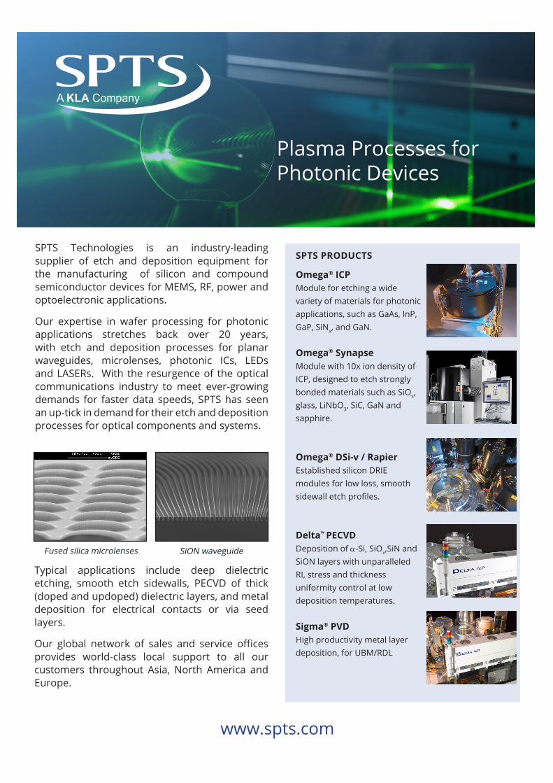
SPTS Technologies is an industry-leading supplier of etch and deposition equipment for the manufacturing of silicon and compound semiconductor devices for MEMS, RF, power and optoelectronic applications.
Our expertise in wafer processing for photonic applications stretches back over 20 years, with etch and deposition processes for planar waveguides, microlenses, photonic ICs, LEDs and LASERs. With the resurgence of the optical communications industry to meet ever-growing demands for faster data speeds, SPTS has seen an up-tick in demand for their etch and deposition processes for optical components and systems.
SPTS PRODUCTS
Omega® ICP Module for etching a wide variety of materials for photonic applications, such as GaAs, InP, GaP, SiNx, and GaN.
Omega® SynapseModule with 10x ion density of ICP, designed to etch strongly bonded materials such as SiOx, glass, LiNbO3, SiC, GaN and sapphire.
Omega® DSi-v / RapierEstablished silicon DRIE modules for low loss, smooth sidewall etch profiles.
Delta™ PECVD Deposition of a-Si, SiOx,SiN and SiON layers with unparalleled RI, stress and thickness uniformity control at low deposition temperatures.
Sigma® PVDHigh productivity metal layer deposition, for UBM/RDL
Fused silica microlenses
Typical applications include deep dielectric etching, smooth etch sidewalls, PECVD of thick (doped and updoped) dielectric layers, and metal deposition for electrical contacts or via seed layers.
Our global network of sales and service offices provides world-class local support to all our customers throughout Asia, North America and Europe.
SiON waveguide
www.spts.com
Plasma Processes forPhotonic Devices
A KLA Company

Etch Processes for Photonics
PECVD Processes for Photonics
Silicon Oxide Etching The Synapse etch system has a unique design which increases the ion density for high oxide etch rates, and the chamber is heated to reduce by-product deposition on the chamber walls to increase MTBC. Deep oxide etches to >100µm can be achieved.
Silicon EtchingSPTS is a recognized leader in deep silicon etching. Our processes offers smooth sidewalls with high etch rates, controlled profile and unique end-point options. Our Rapier DRIE system processes wafers up to 12” in diameter, and can be used for etching Si-SiOx stacks.
Compound Semiconductor EtchingSPTS offers both its standard ICP and Synapse™ technology for etching compound semiconductors. These etch processes can be used to created smooth, vertical or tapered structures to form waveguides, microlenses, modulators, LEDs, and LASERs.
Silicon Oxide / Silicon Oxynitride DepositionThick layers of silicon oxide or silicon oxy-nitride (for example in waveguide manufacturing) require long deposition times and regular chamber cleans. To avoid chamber damage during cleaning, SPTS offers a novel remote plasma cleaning configuration, with end-point control to increase productivity. Film stress <10 MPa is achieved in ≥6µm films, with refractive index tuneable independently of stress.
Amorphous Silicon DepositionTypically used for infra-red waveguide applications where silicon oxide is too lossy, amorphous silicon can be deposited at temperatures < 400°C using PECVD with a silane plasma, which results in a-Si:H film. Minimizing hydrogen content of the films by careful precursor selection and process tuning is key to obtaining low optical loss.
Silicon Nitride DepositionSiN films are widely used as anti-reflective coatings in active photonic devices such as VCSELs. Within wafer and wafer to wafer refractive index and thickness non-uniformities are maintained at <±2% using the Delta™ PECVD system. PECVD SiN is also increasingly used for bow compensation where substrates are kept essentially flat by equalizing the film stresses on both sides, thereby easing subsequent lithography steps.
SPTS Technologies, A KLA company, designs, manufactures, sells, and supports etch, PVD, CVD and MVD® wafer processing solutions for the MEMS, advanced packaging, LED, high speed RF on GaAs, and power management device markets. For more information about SPTS Technologies, email [email protected] or visit www.spts.com© 2019 SPTS Technologies Ltd. All rights reserved. Ref Photonics-Q3/19