pium 4a 5-6-2 en - Strony przedmiotów -...
31
90-924 Łódź, ul. Wólczańska 221/223, bud. B18 tel. 42 631 26 28 faks 42 636 03 27 e-mail [email protected] http://www.dmcs.p.lodz.pl POWER DEVICES AND SYSTEMS LABORATORY Exercise 4 A Full-Bridge Converter Electric Motor Control Indicatory work plan 15′ 30′ 45′ 1 h 1 h 15′ 1 h 30′ After Class 3.2/1–10 3.2/11–19 3.3/1–4 3.3/5–6 3.3/7–12 4 Exercise and manual elaborated by Łukasz Starzak, Andrzej Szajfler Parts C and D (ver. 5.5) translated by Paweł Prędki Łódź 2011 ver. 5.6.2(en). 21.11.2011
Transcript of pium 4a 5-6-2 en - Strony przedmiotów -...

90-924 Łódź, ul. Wólczańska 221/223, bud. B18 tel. 42 631 26 28 faks 42 636 03 27 e-mail [email protected]
http://www.dmcs.p.lodz.pl
POWER DEVICES AND SYSTEMS LABORATORY
Exercise 4A
Full-Bridge Converter Electric Motor Control
Indicatory work plan
15′ 30′ 45′ 1h 1
h15′ 1
h30′ After Class
3.2/1–10 3.2/11–19 3.3/1–4 3.3/5–6 3.3/7–12 4
Exercise and manual elaborated by Łukasz Starzak, Andrzej Szajfler
Parts C and D (ver. 5.5) translated by Paweł Prędki
Łódź 2011
ver. 5.6.2(en). 21.11.2011


© 2011 Łukasz Starzak, Katedra Mikroelektroniki i Technik Informatycznych Politechniki Łódzkiej
Contents
B Exercise Introduction ...................................................................................................................... 5
1. Exercise Aim and Plan.........................................................................................................................................5
2. Insulated Gate Bipolar Transistor ....................................................................................................................7
2.1. Recommended reading.............................................................................................................................7
C Experiment ........................................................................................................................................ 9
3. Measurements .......................................................................................................................................................9
3.1. Test circuit ..................................................................................................................................................9 3.2. Preparation for measurements.............................................................................................................11
Measurement set-up configuration ............................................................................................ 11 Test measurement........................................................................................................................... 12
3.3. Measurement procedure........................................................................................................................14 Full switching cycle ........................................................................................................................ 14 Detailed switching observation ................................................................................................... 15 Measurement termination ............................................................................................................ 17
D Results.............................................................................................................................................. 19
4. Result Elaboration and Analysis .....................................................................................................................19
4.1. Stationary state parameters ..................................................................................................................19 4.2. Turn-on and turn-off parameters........................................................................................................21
Starting Scilab .................................................................................................................................. 21 Time-related parameters ............................................................................................................... 21 Energy-related parameters ........................................................................................................... 21 Further cases..................................................................................................................................... 22
4.3. Current tail parameters..........................................................................................................................25 4.4. Result recapitulation...............................................................................................................................26 4.5. Result analysis..........................................................................................................................................27
Time-related parameters ............................................................................................................... 27 Energy-related parameters ........................................................................................................... 27 Comparison of field effect transistors........................................................................................ 27
E Information ..................................................................................................................................... 29
5. Expected Report Contents................................................................................................................................29
6. Required Knowledge..........................................................................................................................................30
6.1. Prerequisites .............................................................................................................................................30 6.2. Test scope..................................................................................................................................................30
7. References ............................................................................................................................................................31


© 2011 Łukasz Starzak, Katedra Mikroelektroniki i Technik Informatycznych Politechniki Łódzkiej
B
Exercise Introduction
1. Exercise Aim and Plan
The aim of this exercise is first to get acquainted with yet another work configuration of power semiconductor devices, the bridge. Second, electric motor control will be taken advantage of as a practical application example.
Generally speaking, both these issues are fairly complex due to the large number of possible control strategies for bridge switches as well as the multitude of motor solutions. For this reason, we will restrict to a control method that is simple and yet enables a complete analysis of the circuit. Also the motor chosen—a permanent magnet DC one—is among all the electric motors the easiest one to control. It will enable gaining the most basic knowledge about the specificity of power converter operation with RLE receivers. A DC/DC bridge converter will be the power converter used in this exercise.
Converter characteristics will be determined in this exercise, including those independent and those dependent on the receiver, as well as one of the typical characteristics of the electric motor. On the other hand, the operation of the DC/DC bridge converter will be investigated at the current and voltage level, including drive circuits of the transistor switches.


© 2011 Łukasz Starzak, Katedra Mikroelektroniki i Technik Informatycznych Politechniki Łódzkiej
2. Insulated Gate Bipolar Transistor
2.1. Recommended reading
Ref. Textbook Excerpt Equivalent in the Polish Manual
Complementary Reading
Complements in this Manual
A Bal 8, 8.1, 8.2, 8.2.1, 8.2.2, 8.3, 8.3.1, 8.3.2
2.1, 2.2
B Bal 8.6, 8.6.1 2.3.c, 2.5 [21] 8.5 Switching Times, Switching Energy
C Bal 8.2.2, 8.3.2, 8.6.2.3, 8.7
2.4

© 2011 Łukasz Starzak, Katedra Mikroelektroniki i Technik Informatycznych Politechniki Łódzkiej
C
Experiment
3. Measurements
3.1. Test circuit
The schematic diagram of the laboratory circuit is presented in Fig. 1. The circuit allows measurement of terminal voltages and collector current of the transistor under investigation which is IRG4BC20S.
Element values are as follows:
load resistance: R1 = 4,7 Ω,
gate resistance: RG = 10 Ω; 150 Ω; 300 Ω; 600 Ω.
The purpose of the switches found on the panel is as follows:
K1 enables selecting the circuit configuration (0/L/H/P), the ‘L’ being the only one used in this exercise,
K2 enables selecting the load configuration (R/RL/RLD), the resistive one with the R1 resistor being the only one used in this exercise,
K5 enables changing the gate resistance RG by connecting an appropriate resistor.
In order to eliminate the influence of self-heating on the transistor under test as well as to allow measurement of significant currents without the risk of thermally damaging the transistor, the measurements are conducted using single switching pulses (turning the transistor on and back off after a short period of time). A rectangular pulse of the ug voltage is generated each time the green button located on the front panel is pressed (switch K4 in Fig. 1); the pulse width tp is of several dozen microseconds and its amplitude is approximately equal to the control (drive) circuit supply voltage UGG. This voltage, equal to 15 V, is generated internally with a built-in power supply supplied from the 230 V mains.
Taking the above into consideration, it is required to generate a switching pulse every time settings have changed. This also applies to situations where changes are only made in the measurement equipment (oscilloscope, current probe). Only after a new pulse is generated will the oscilloscope capture waveforms using the new settings and the changes will have their effect. Until then, waveforms will not change, even though they may appear to do so (i.e. horizontal waveform

10 C 3 Power Devices and Systems. Exercise 4A. Insulated Gate Bipolar Transistor (5.6.2)
© 2011 Łukasz Starzak, Katedra Mikroelektroniki i Technik Informatycznych Politechniki Łódzkiej
magnification by changing the time base). The oscilloscope memory will still contain the old data and the plot points will just be stretched along the time axis. This mechanism resembles digital zoom—it does not allow to capture a more precise image but only stretches it. The oscilloscope used in the laboratory indicates tjis by greying out waveforms. The above also applies to vertical magnification of the plots (i.e. changing the voltage gain of the oscilloscope or the conversion factor of the current probe).
K4
K2
Built-in Power
AC 230V
/ DC 15V
Pulse Generator
D3
Us
~230V
UCC
R3
T
vE
L3
vC
Gate Driver
UGG
R1
RG
–
vG
L2
K3
iC
R2
K5
+
Supply
Fig. 1. Schematic diagram of the test circuit for investigation of dynamic properties of a standard IGBT (for the K1 switch set in the L, low-side switch, position)
Voltage measurements are performed using voltage probes appropriately connected to the banana sockets found on the circuit’s panel, labelled vE, vG and vC. For this purpose, banana connectors are provided that enable attaching a probe.
Collector current measurement is performed by clamping a current probe around the wire led out above the panel, labelled iC (whose location within the circuit is marked with an arrow in Fig. 1). The arrow on the current probe body indicates the positive reference direction. The clamping should be done in such a way that the probe reference direction agrees with the one in the schematic diagram.
For recording data from the oscilloscope, the WaveStar for Oscilloscopes application should be used which is accessible through the Start Menu, Pomiary tab, in a way described later in this manual.

Measurements C 3 11
© 2011 Łukasz Starzak, Katedra Mikroelektroniki i Technik Informatycznych Politechniki Łódzkiej
3.2. Preparation for measurements
Measurement set-up configuration
In order to save time, execute next steps concurrently with step 1.
1. Turn on the computer. After log-on is completed, turn on the oscilloscope and configure the connection to the computer, strictly following the additional instructions available at the laboratory stand. (If the team has already used the TDS224 oscilloscope before, its configuration should not be necessary now unless communication problems occur.)
2. Make sure that the built-in 15 V power supply is turned off (the K3 switch set to OFF). Plug the power connector in.
3. Set up internal connections of the laboratory circuit:
choose the low-side switch topology by setting the K1 switch to L,
choose the resistive receiver R1 by setting the K2 switch to R,
plug the PB wire into the GND.LHP socket.
4. Use a power supply with two adjustable sections to power the circuit. Before connecting, make sure that it is switched off. Connect the outputs of one of the adjustable sections to the UCC (not V ZAS H) on the circuit’s panel.
5. Switch the power supply into the independent operation mode (two buttons in the middle of the front panel). Turn all the knobs down to zero (extreme counterclockwise position).
6. Attach 10:1 attenuation voltage probes to the circuit so that to measure the transistor’s gate-emitter voltage uGE in channel 1 and its collector-emitter voltage uCE in channel 2.
Warning!
1. The ground leads (alligator clips) of the voltage probes are mutually shorted inside the oscilloscope and connected to the protective earth of the mains; both of them must therefore be always connected to the same potential. Any other configuration may cause a significant current to flow through the oscilloscope and damage its input circuitry.
2. Do not touch the elements at which the power circuit supply voltage is present (especially the vC potential connector) during measurements.
3. Before proceeding, connections must be checked by the teacher.
7. Turn on the built-in 15 V power supply with the K3 switch. The green LED indicator should turn on.
Before proceeding, read the next step instructions entirely together with additional remarks!
8. Turn on the external power supply. Slightly increase the current limiter threshold (Current knob) of the section supplying the power circuit until the red LED indicator (C.C.) turns off. Set the voltage (Voltage knob) to 60 V. A green LED indicator on the circuit’s panel should turn on.
When the circuit operates correctly, the only current indicated by the power supply’s ammeter should be a constant LED indicator current (approx. 0,01 A) and a possible transient current charging the blocking capacitor inside the circuit (not more than 0,05A). If anything else is observed during adjustment or later, turn off the power supply immediately and ask the teacher to check the circuit once again.
9. Increase the current limiter threshold of the section supplying the power circuit to the maximum (extreme clockwise knob position).
10. Using the CH1/2/3/4 buttons on the oscilloscope, display the waveform from channel 1 and hide waveforms from all the other channels.

12 C 3 Power Devices and Systems. Exercise 4A. Insulated Gate Bipolar Transistor (5.6.2)
© 2011 Łukasz Starzak, Katedra Mikroelektroniki i Technik Informatycznych Politechniki Łódzkiej
Pressing the MENU button of a given channel toggles between displaying and hiding the corresponding waveform. When a given waveform is displayed, this is indicated by an arrow pointing at zero level left of the graticule and by a “CHx” symbol below the graticule.
Test measurement
11. Use the K5 switch to select the 600 Ω gate resistor.
12. Configure the oscilloscope:
(a) channel 1 (CH1 MENU button):
Coupling: DC,
Probe: 10x,
Invert: Off,
gain adequate to the expected amplitude of the uGE voltage (CH1 VOLTS/DIV knob; the current setting is displayed next to the channel symbol CH1);
(b) time base:
trigger moment approximately in the middle of the screen (HORIZONTAL POSITION knob; current setting is indicated by the arrow above the graticule),
time base appropriate for the expected duration of the driving pulse width (SEC/DIV knob; current setting is displayed under the graticule next to the M symbol);
(c) triggering (TRIGGER MENU button):
edge trigger,
trigger on the rising slope,
the uGE waveform as the triggering source (appropriate channel number in the Source field),
normal mode,
coupling with noise rejection,
trigger level at approximately half the expected range of the uGE voltage (TRIGGER LEVEL knob; current setting is displayed under the division line next to the CH1 trigger channel symbol and the edge symbol ).
13. Press the green K4 button in order to generate a transistor switching pulse. A “Trig’d” message should appear briefly on the oscilloscope screen above the graticule and the uGE voltage waveform should be displayed. If this does not happen, check the oscilloscope settings (especially the channel 1 amplification Volts/Div, the time base Sec/Div and the trigger level Level). If this does not help, ask the teacher to check the settings.
14. Adjust (generating the switching pulse after each change of settings) the time base and trigger moment position (SEC/DIV and HORIZONTAL POSITION knobs) so that the pulse of the uGE voltage is visible in its entirety (see Fig. 2) and occupies most of the screen horizontally.
15. Display the channel 2 waveform, which is the uCE voltage, using the CH2 MENU button. Check:
whether channel settings agree with those given in step 12(a), modifying them if necessary,
whether the waveform does not go beyond the screen (ignore possible short spikes) or whether its amplitude is not too low (not clearly visible), adjusting the gain and the zero level if necessary (VOLTS/DIV and VERTICAL POSITION knobs),
whether the waveform is correct (see Fig. 2).
16. Following the additional manual available and the laboratory stand, configure the current probe amplifier and its connection to the oscilloscope. Read and apply obligatorily all the guidelines given in that manual pertinent to oscilloscope configuration.
At the proper time:
attach the amplifier’s output to channel 4;

Measurements C 3 13
© 2011 Łukasz Starzak, Katedra Mikroelektroniki i Technik Informatycznych Politechniki Łódzkiej
adjust the current/voltage conversion factor so that it is possible to measure and display a waveform of the expected amplitude on the oscilloscope (see information about probe amplifier operation and its coupling with the oscilloscope given in the probe manual; calculate the amplitude using the known parameters of the receiver and power supply assuming that the main terminals of the transistor are perfectly shorted).
Fig. 2. The waveforms of uGE, uCE and iC during one switching cycle of an IGBT with resistive load
17. Apart from the adjustments indicated in the current probe instructions, set:
(a) on the probe amplifier, DC coupling;
(b) on the oscilloscope (CH4 MENU):
DC coupling,
invert de-activated (off).
18. Clamp the current probe around the appropriate wire so that to measure the collector current iC and so that the measured current direction agrees with the real one.
19. Generating the switching pulse, adjust:
amplification along the measurement path as described in the manual:
[A6302/A6312+AM503B] on the probe amplifier, not the oscilloscope,
[TCP312+TCPA300] at channel 4 of the oscilloscope, not the probe amplifier, unless the amplification setting on the amplifier is incorrect (which may be reflected in a current waveform far from a rectangular pulse, among others),
waveform position using the channel 4 VERTICAL POSITION knob (on the oscilloscope),
so that the current waveform is displayed optimally, i.e. maximally fills the screen vertically but does not go beyond the screen. Check that the waveform is correct (see Fig. 2).
If the the current/voltage conversion factor of the probe amplifier has been significantly changed (by an order of magnitude or more), repeat the calibration and de-gauss procedure after closing the probe without any wire inside.

14 C 3 Power Devices and Systems. Exercise 4A. Insulated Gate Bipolar Transistor (5.6.2)
© 2011 Łukasz Starzak, Katedra Mikroelektroniki i Technik Informatycznych Politechniki Łódzkiej
3.3. Measurement procedure
Full switching cycle
1. Generate a switching pulse. Make sure that the image of the waveforms is still correct. Check if the current pulse amplitude as seen on the oscilloscope is approximately equal to the one calculated in step 3.2/16 (see the guideline concerning reading out the voltage/current conversion factor in the current probe manual).
Skipping the above step may cause result processing to become impossible!
Although the current consumption period is short, it significantly exceeds the output current capability of the power supply. Due to this fact, sometimes the current limiter may be activated, limiting both current and voltage. Because of that, after generating a switching pulse make sure that the on-state iC current value and off-state uCE voltage value (equal to the power supply voltage UCC) observed on the oscilloscope are correct. Otherwise, generate a switching pulse again.
2. Adjust, if necessary:
the gain of the voltage measurement channels (1 and 2) using the VOLTS/DIV knob,
the amplification along the current measurement path as described in the current probe manual:
[A6302/A6312+AM503B] on the probe amplifier, not the oscilloscope,
[TCP312+TCPA300] at channel 4 of the oscilloscope, not the probe amplifier,
waveform position using the VERTICAL POSITION knobs,
so that each waveform, from its zero level (indicated by an arrow left of the graticule) to its peak value maximally fills the entire screen area vertically but does not go beyond the screen (still ignoring possible short spikes).
3. [A6302/A6312+AM503B] The current probe used passes the DC component of waveforms incorrectly, which may cause improper indication of the zero level of the current. As a result:
ensure that the collector current displayed on the oscilloscope is found at the zero level (marked with an arrow with channel number) within the interval where the transistor is off (zero drive voltage uGE);
if it is not found at this level, manually shift the waveform vertically as appropriate, using the Output DC Level knob on the current probe amplifier (not the Vertical Position knob on the oscilloscope);
if needed, correct the position of the current waveform on the oscilloscope’s screen using the appropriate Vertical Position knob on the oscilloscope.
Waveform correctness from the above point of view should be checked each time before waveforms are downloaded from the oscilloscope.
4. Save the set of the three waveforms (uGE, uCE and iC, together):
(a) in the WaveStar application, create a new sheet of the YT Sheet type;
(b) from the side panel (Local oscilloscope name Data Waveforms channel symbol), drag the three waveforms displayed on the oscilloscope to the new sheet;
After waveforms have been dragged once, it is sufficient to just refresh them later by pressing the Refresh Sheet button or selecting the View, Refresh Datasheet from the menu.
A plot can be removed from a sheet by clicking its number left to the graticule and pressing the Delete key.
(c) save the sheet containing all the three plots in the WaveStar application format (SHT) using the Save Datasheet button (Ctrl+S);

Measurements C 3 15
© 2011 Łukasz Starzak, Katedra Mikroelektroniki i Technik Informatycznych Politechniki Łódzkiej
Don’t use the Save Worksheet function which does not save any measurement data, just the names of the sheets being currently open.
(d) write down the current probe amplification setting (see the current probe manual; a Notes Sheet may be used for this purpose).
Detailed switching observation
5. Record waveforms enabling determining time and energy-related dynamic parameters describing transistor’s turn-on (not any other operating state):
(a) adjust the time base (SEC/DIV), trigger moment position (HORIZONTAL POSITION) and possibly the trigger level (LEVEL) so as to observe the turn-on (not any other operating state) of the transistor with as much accuracy as possible, considering phenomena in the transistor’s main circuit, i.e. the ton time interval (see Fig. 2);
Fig. 3. The most important IGBT dynamic parameters (the plots do not reproduce the exact waveforms)
(b) make sure that all the threshold crossing moments are visible on the screen enabling determining the time-related parameters for turn-on (see Fig. 3);
(c) make sure that channel settings still meet the requirements of given in step 2, however, taking possible overvoltages into consideration now;
(d) [A6302/A6312+AM503B] check and (if needed) modify the current measurement path settings according to step 3;
(e) in the WaveStar application, create two new sheets one YT sheet and one Power Harmonics;

16 C 3 Power Devices and Systems. Exercise 4A. Insulated Gate Bipolar Transistor (5.6.2)
© 2011 Łukasz Starzak, Katedra Mikroelektroniki i Technik Informatycznych Politechniki Łódzkiej
The Power Harmonics sheet allows, among others, multiplying two waveforms. If these two waveforms are a current i flowing between two circuit nodes and the voltage u between these nodes, then the obtained i∙u product will by definition be the instantaneous power p dissipated in the components located between these two nodes.
(f) use the Power Harmonics sheet to calculate the instantaneous power loss pC waveform:
drag the iC current waveform from the side panel to the Current Waveform window at the bottom of the Power Harmonics sheet;
drag the voltage waveform appropriate for obtaining the power loss in the transistor’s collector circuit pC (not any other waveform product) to the Voltage Waveform window;
(g) drag all the four waveforms, uGE, uCE, iC and pC, to the YT Sheet;
In order not to waste time downloading the waveforms again from the oscilloscope (this action will be repeated several times), all the three waveforms already displayed in the Power Harmonics sheet should be dragged from that sheet and not from the side panel. Only the missing waveform can be dragged from the side panel.
Do not change any settings in the WaveStar application until all measurements described in this manual are finished. The only exceptions are:
changing the colour from the toolbar at the top of the sheet’s window;
moving the zero level using the arrow left of the graticule;
moving the trigger moment position as described in sub-step (h).
All other changes will cancel the possibility of refreshing the sheets, which will significantly increase the amount of time needed to complete the exercise.
(h) it is usually necessary to synchronise the power waveform with the others; to achieve this, select the power waveform by clicking its number left of the graticule, then move the coloured slider above the graticule, positioning it exactly between the white markers in the shape of square brackets;
(i) Save the YT Sheet containing the complete set of four waveforms and write down the current probe amplification setting (if it has changed).
6. Change the gate resistance to 300 Ω and repeat step 5, however, instead of creating new sheets and dragging the waveforms [sub-steps (e)—(g)], just do the following:
first, instead of sub-step (f), refresh the Power Harmonics sheet (Refresh Sheet button or View, Refresh Datasheet from the menu),
next, instead of sub-step (g), refresh the YT Sheet.
7. * Repeat step 6 for RG = 150 Ω.
8. Record waveforms enabling determining time and energy-related dynamic parameters describing transistor’s turn-off:
(a) switch to falling-edge uGE waveform triggering (TRIGGER MENU, Slope);
(b) repeat step 5, but:
instead of transistor’s turn-on, its turn-off during the toff time interval should obviously be considered as defined based on physical phenomena (i.e., not according to technical definitions but according to Fig. 2);
The above sub-step does not tell to observe any fragment of the toff time interval, but the toff time interval, meaning this entire time interval. Incorrect execution of this sub-step will make it impossible to obtain results required and measurements will have to be repeated. In case of doubts, study the abovementioned figure once again considering all the three waveforms displayed on the oscilloscope and consult your result with the teacher.
pay special attention to performing sub-step 5(d) (if the relevant probe and amplifier are used);

Measurements C 3 17
© 2011 Łukasz Starzak, Katedra Mikroelektroniki i Technik Informatycznych Politechniki Łódzkiej
Due to the current tail occurring, the collector current should be found at the zero level only after the tail ends and not when the drive voltage uGE falls down to zero (see Fig. 2). In case of doubt, consult the oscilloscope image with the teacher.
instead of creating new sheets and dragging the waveform [steps (e)—(g)], just first refresh the Power Harmonics sheet and then, the YT Sheet.
9. Repeat step 8 for RG = 600 Ω.
10. * Repeat step 9 for RG = 150 Ω.
Measurement termination
11. [A6302/A6312+AM503B] On the current probe amplifier, bring the Output DC Level knob setting to the value of 0.0 (the setting is displayed in the Current/Division field during adjustment).
12. Decrease the supply voltage of the external power circuit to zero. Wait until the green LED on the circuit’s panel goes out. Turn off the power supply.
13. Switch the built-in 15 V power supply off and unplug it from the mains.


© 2011 Łukasz Starzak, Katedra Mikroelektroniki i Technik Informatycznych Politechniki Łódzkiej
D
Results
4. Result Elaboration and Analysis
4.1. Stationary state parameters
1. Start the WaveStar application.
2. Open the waveform set uGE; uCE; iC for the full driving voltage pulse, registered in step 3.3/3.
3. Based on of the current probe’s current/voltage conversion factor written down, calculate the coefficient ki in amps per volt, which will be used to multiply a value shown in WaveStar in volts in order to obtain a corresponding real current value in amps.
Values shown in WaveStar for current waveforms are indeed voltage values that came from the current probe amplifier and were registered by the oscilloscope. We will denote this with an asterisk. Such a voltage is proportional to the current according to the current probe conversion factor written down. The coefficient, resulting directly from this factor, but expressed in SI units, i.e. A/V, for practical reasons, will allow obtaining real values in amps. (According to the A6302/A6312+AM503B current probe and amplifier manual, the value indicated on the display was expressed in A/10 mV or in mA/10 mV.) If, for example, the current probe conversion factor has been 5 A / 10 mV, then ki = 5 A / 10 mV = 500 A/V. The real value of current in amps is i [A] = ki [A/V] ∙ i* [V].
4. Verify the correctness of the current value conversion:
(a) using a horizontal cursor, read out the drain current value IC(on)* (in volts);
Slight overshoots that sometimes may be seen in the current waveform (upwards after turn-on, downwards after turn-off), result only from the limited frequency bandwidth of the current probe. They should be therefore neglected during analysis. If there is an overshoot with considerable amplitude, it should be assumed that the high level of the current pulse is indeed a horizontal line at the level that the waveform attains after the visibly faster growth in the beginning of the pulse.
Remarks on the use of cursors in the WaveStar software:
1. In order to activate cursors, chose View Properties Cursor from the menu and select a cursor type appropriate for the measurement. In the active YT Sheet, values related to the active waveform will appear, depending on the cursor type selected:

20 D 4 Power Devices and Systems. Exercise 4A. Insulated Gate Bipolar Transistor (5.6.2)
© 2011 Łukasz Starzak, Katedra Mikroelektroniki i Technik Informatycznych Politechniki Łódzkiej
— X, Y – the coordinates of the active cursor (continuous line);
— X1, Y1 and X2, Y2 – the coordinates of the first and the second cursors;
— dX, dY – the differences of the two cursors’ coordinates.
2. A waveform can be activated by clicking its number shown left of the graticule. The number of the active waveform is constantly highlighted.
3. After switching to another waveform, a horizontal cursor remains on the same level in volts (not in divisions). This means that when a large difference in vertical scales (V/div) is present between the two waveforms, the cursor can be placed beyond the display. In such a situation, temporarily increase the V/div coefficient, then move the cursor to a level close to zero and after that restore the previous coefficient value.
4. Distinguishing different waveforms will be easier when coloured legend is chosen: in the menu View Properties Plot, select Waveform notes color match waveform color.
(b) using the coefficient ki determined in step 3, calculate the real drain current value (in amps) IC(on);
(c) check if the IC(on) value determined conforms with test circuit data and settings [see Section 3.1 and step 3.2/16]; if not, identify the source of this discrepancy (e.g. an improper gain setting on channel 4 of the oscilloscope different from 10 mV/div in the case of the A6302/A6312+AM503B current probe and amplifier, a mistakenly noted current probe amplifier indication, wrong load resistor network configuration) because the ki coefficient is very important for calculations that follow.
5. Based on the oscilloscope image, determine the voltage and current thresholds necessary for using the technical definitions of the time-related dynamic parameters (see Fig. 3 and Ref. 21, Section 8.5):
(a) using a horizontal cursor, read out the on-state gate-emitter voltage value UGE(on);
(b) calculate the threshold values used in the technical definitions of the time-related dynamic parameters (for current also in volts as it will be easier to read values out of oscilloscope images).

Result Elaboration and Analysis D 4 21
© 2011 Łukasz Starzak, Katedra Mikroelektroniki i Technik Informatycznych Politechniki Łódzkiej
4.2. Turn-on and turn-off parameters
Starting Scilab
1. Run the numerical computation package Scilab.
2. Load the script that contains functions necessary for dissipated energy calculation by executing the command:
exec('script_path\wavestar_calka.sce');
where script_path is the path for the file wavestar_calka.sce.
3. In order not to have to enter the full path for all the processed files (WaveStar output files), the working directory may be changed to the directory that contains them by executing the command:
cd('measurement_path’);
Time-related parameters
4. In WaveStar, open the waveform set uGE; uCE; iC; pC for the turn-on process, for RG = 600 Ω, registered in step 3.3/5.
5. In the WaveStar software determine the time-related dynamic parameters for turn-on:
(a) using paired cursors, read out the turn-on delay time td(on) according to its technical definition, using the thresholds calculated in step 4.1/5 (see Fig. 4);
Exemplary readings presented on the figures in this sub-section show only the way how the parameters should be measured. They do not suggest any correct values, and the way that waveforms should look like in the sheet. In order to get exemplary results more readable, oscilloscope images contain only waveforms necessary to understand particular section.
(b) using paired cursors, read out the rising time tr according to its technical definition.
Energy-related parameters
6. Based on the current probe current/voltage conversion factor written down, determine the ki coefficient for the oscilloscope image currently processed (if the amplification setting was not changed, this is not necessary as the value calculated in step 4.1/3 remains valid).
7. In WaveStar, determine the parameters of the power pulse generated during turn-on:
(a) using cursors, read out the coordinates of the time moments tinf(on) and tsup(on) that correspond to the beginning and the end of the power pulse;
For simplicity, disregard the voltage and current thresholds. Base mainly on the instantaneous power waveform pC assuming that it is sufficient to distinguish dynamic states from static ones (see Fig. 5). Refer to the uGE voltage waveform as well in case of doubt (especially to determine the turn-on end and the turn-off beginning).
(b) export the data to a CSV (comma-separated values) text file from the menu File Export Datasheet CSV.
8. In Scilab, calculate the energy dissipated during turn-on WC(on):
(a) read in the data exported by executing the command
[header,data]=wczytaj_ws('file_name.csv');

22 D 4 Power Devices and Systems. Exercise 4A. Insulated Gate Bipolar Transistor (5.6.2)
© 2011 Łukasz Starzak, Katedra Mikroelektroniki i Technik Informatycznych Politechniki Łódzkiej
During calculations for subsequent cases, a previously executed command can be recalled by pressing the up-arrow on the keyboard.
(b) calculate the energy WC(on) as the integral of pC for the interval from tinf(on) to tsup(on), taking the ki coefficient into account, by executing the command:
calka_infsup(data,pc_waveform_no,tinf,tsup,pd0,ki)
The parameter pc_waveform_no is the number of the pD waveform according to the increasing numbering in WaveStar software (not the channel number on the oscilloscope). If, for example, waveforms displayed in WaveStar are: 2) uCE, 3) iC, 4) pC, 6) uGE, then the pC waveform is the third consecutive, so pc_waveform_no = 3 should be entered; if numbering starts from 1 and there is no gap, then pc_waveform_no is identical to the one shown in WaveStar.
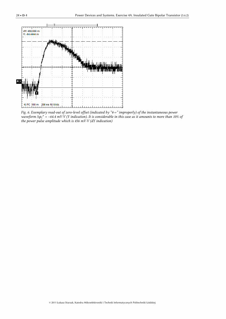
The parameter pc0 allows taking into account the zero level shift of the pC waveform (non-zero value in the off-state) caused by imperfection of the current probe. If this shift is considerable, then the false (non-zero) value of pC indicated in WaveStar in the off-state should be entered (in V∙V without converting to watts, see Fig. 6, lower cursor position). If the shift is small as compared to the power pulse amplitude, enter 0.
An alternative version of the integral function can be used, calka_infdelta(). It works in a way identical to the previous one except that instead of tsup, the parameter deltat = tsup(on) − tinf(on) should be entered. It may be more convenient because both readings (X and dX) can be copied from the YT Sheet at the same time.
An example, assuming that the sequence of waveform presentation in WaveStar has been as follows: 1) uCE, 2) iC, 3) uGE, 4) pC, and that other parameters have had values as in the exemplary figures 5 and 6 (see figure labels):
calka_infsup(dane,4,0.02E-6,1.26E-6,-64.4E-3,200)
or
calka_infdelta(dane,4,0.02E-6,1.24E-6,-64.4E-3,200)
(c) the above function returns the value of the integral in joules and, for verification purposes, plots the pC waveform shifted by pC0 and scaled by ki as well as fills the area that corresponds to the calculated integral;
based on this plot check, verify whether the integral has been calculated for a proper interval along the power waveform, i.e. for a pulse that can be clearly distinguished from the off-state that precedes it and from the turn-on state that follows, and that the pulse base level is found at the real zero level, i.e. the constant value of the waveform in the off-state, and if not, calculate the energy again;
(d) save the plot check selecting File Export from the menu (GIF or EMF format should be used).
Further cases
9. Repeat steps 4—8 for the RG = 300 Ω (* and RG = 150 Ω) case, based on the waveforms recorded in step 3.3/6 (* and 3.3/7).
10. Repeat steps 4—8 for the turn-off state, for RG = 600 Ω, 300 Ω (* and 150 Ω) so as to determine the time-related dynamic parameters td(off) and tf and the energy-related one WC(off), based on the waveform sets recorded in steps 3.3/9, 8 (* and 10).
11. * Repeat steps 4—8 for the IRG4BC20U transistor (RG = 600 Ω) for both turn-on and turn-off states so as to determine the time-related parameters td(on), tr, td(off), tf and the energy-related ones WC(on), WC(off).

Result Elaboration and Analysis D 4 23
© 2011 Łukasz Starzak, Katedra Mikroelektroniki i Technik Informatycznych Politechniki Łódzkiej
Fig. 4. Exemplary read-out of the td(on) = 250 ns time (dX indication). The Y value shows that the right cursor has been positioned just after the iC waveform crosses the 10% IC* level which has been 58.7 mV in this case.
Fig. 5. Exemplary read-out of tinf(on) = 0.02 µs (left cursors, X indication) and tsup(on) = 1.26 µs (∆t = 1.24 µs, dX indication) times
24 D 4 Power Devices and Systems. Exercise 4A. Insulated Gate Bipolar Transistor (5.6.2)
© 2011 Łukasz Starzak, Katedra Mikroelektroniki i Technik Informatycznych Politechniki Łódzkiej
Fig. 6. Exemplary read-out of zero-level offset (indicated by “4->” improperly) of the instantaneous power waveform ∆pC* = −64.4 mV∙V (Y indication). It is considerable in this case as it amounts to more than 10% of the power pulse amplitude which is 456 mV∙V (dY indication)

Result Elaboration and Analysis D 4 25
© 2011 Łukasz Starzak, Katedra Mikroelektroniki i Technik Informatycznych Politechniki Łódzkiej
4.3. Current tail parameters
1. Based on the oscilloscope image for turn-off, for RG = 600 Ω, determine the current tail parameters:
(a) use cursors to determine the current tail amplitude Itail (see Fig. 2);
(b) use cursors to determine the approximate current tail duration tf,tail assuming the criterion of falling to about 5% of its initial value Itail for determining its end (see Fig. 2);
(c) use a cursor to determine the time coordinate of the beginning of the current tail tinf(tail) (the beginning of the tf,tail interval, the t7 moment in Fig. 2);
(d) following the same procedure as for the WC(off) energy, calculate in Scilab the energy component WC(off,MOS) related to the turn-off of the MOS component of the transistor (see Fig. 3) as an integral over the time interval from tinf(off) (which value has been determined in step 4.2/10) to tinf(tail); save the plot check;
(e) Calculate the WC(off,tail) energy component as the difference between the total energy WC(off) and the WC(off,MOS) energy.
2. Obtain plots that will enable comparing current tails for different operating conditions:
Numerical comparison of current tail parameters is difficult because of the high measurement uncertainty (see Ref. 21). We will therefore rely on graphical analysis partly.
(a) from the YT Sheet for turn-off at Rg = 600 Ω, remove all the waveforms except the iC current one;
(b) making use of the possibility to move waveforms between sheets, add the iC current waveform from the YT Sheet containing results for turn-off at RG = 300 Ω (* and at 150 Ω);
(c) if time scales (as indicated in the legend) of different waveforms differ, make them the same using the pull-down list found in the toolbar in the YT Sheet window, or selecting View > Properties from the menu, switching to the appropriate waveform tab and setting Horizontal Scale;
(d) synchronise the waveforms with respect to the beginning moment of the current tail using the slider above the graticule (i.e. move waveforms horizontally so as all the current tails originate from the same moment);
(e) set zero levels (i.e. current levels in the off-state) of all the waveforms at the same level dragging their numbers left to the graticule, or selecting View > Properties from the menu, switching to the appropriate waveform tab and setting Vertical Position;
(f) save the obtained sheet under a new file name.

26 D 4 Power Devices and Systems. Exercise 4A. Insulated Gate Bipolar Transistor (5.6.2)
© 2011 Łukasz Starzak, Katedra Mikroelektroniki i Technik Informatycznych Politechniki Łódzkiej
4.4. Result recapitulation
1. Gather the results obtained in Section 4.2 in a table (or possibly two tables, for turn-on and turn-off separately) containing the following parameters for both (* all three) RG cases:
RG;
td(on), tr, WC(on) for turn-on;
td(off), tf, WC(off) for turn-off.
2. Calculate (see Fig. 3 and Ref. 21) and add to the table directly following the respective time-related parameters:
(a) the total turn-on time ton;
(b) the total turn-off time toff;
3. In a separate row, calculate the rates of change (i.e. values telling how many times a parameter has changed, not by what amount it has) for all the above parameters (RG included) with the resistance changing from the smaller to the larger one (not the opposite) (* disregard the smallest of the three resistances).
4. Gather the current tail parameters determined in step 4.3/1.
5. * Plot as function of the gate resistance RG:
(a) the time-related parameters td(on), tr, td(off), tf (all in one graph);
(b) the energy-related parameters td(on), tr, td(off), tf (both in one graph).

Result Elaboration and Analysis D 4 27
© 2011 Łukasz Starzak, Katedra Mikroelektroniki i Technik Informatycznych Politechniki Łódzkiej
4.5. Result analysis
Time-related parameters
1. Based on results found in the table (* and shown in the plots), determine the effect of the gate resistance value RG on each of the time-related transistor parameters: td(on), tr, ton as well as td(off), tf, toff. Consider both the direction and the magnitude of the change (i.e. how many times parameter values change as compared to the rate of change of RG).
2. Based on turn-off collector current waveforms, as observed in the comparison image obtained in step 4.3/2, state whether the gate resistance has any effect on current tail duration and amplitude and if so, to what extent.
3. Compare the current tail duration ttail and the fall time tf. Comment on the results of this comparison in respect of practical usefulness of the tf parameter for evaluating turn-off duration and energy dissipation in the case of the IGBT.
Energy-related parameters
4. Based on the tabulated current tail parameters, calculate the percentage contribution of the WC(off,tail) and WC(off,MOS) components to the total energy dissipated during turn-off WC(off).
State how the current tail-related energy dissipation WC(off,tail) relates to the MOS component turn-off-related energy dissipation WC(off.MOS) (is it approximately equal or much lower or greater, by what ratio?)
5. Based on results found in the table (* and shown in the plots) determine the effect of the gate resistance on each of the energy-related parameters of the transistor WC(on) and WC(off). Consider both the direction and the magnitude of the change (i.e. how many times parameter values change as compared to the rate of change of RG).
6. Recapitulate whether the circuit designer is able to influence all the dynamic parameters (both time and energy-related) of the IGBT through the gate resistance RG to the same extent. Which parameters can visibly be influenced less significantly and how does this follow from the physical principles of operation of the IGBT (see Ref. A)?
Comparison of field effect transistors
7. * Based on results from this exercise and from the exercise 3A, compare the dynamic properties
of two types of power field effect transistors, the IGBT and the MOSFET. In the analysis include:
(a) the shapes of the waveforms and the consequences they have for time and energy-related parameters;
(b) changes of time and energy-related parameters as functions of the gate resistance.
Numerical values as such should not be compared as transistors had different ratings. It is therefore natural that their electrical parameters are different and no conclusion can be drawn out of this fact. Transistors with similar ratings that enable such a comparison to be made, are analysed (in static aspect) in Exercise 5
A.


© 2011 Łukasz Starzak, Katedra Mikroelektroniki i Technik Informatycznych Politechniki Łódzkiej
E
Information
5. Expected Report Contents
Oscilloscope image of voltages and current for a full driving voltage pulse, labelled with the current probe current/voltage conversion factor (i.e., the set of waveforms uGE; uCE; iC)
Numerical values of characteristic levels with their justification and the calculated threshold values necessary for determination of time-related parameters, according to step 4.1/5
All the oscilloscope images that have been used to determine the time-related and energy-related parameters of the transistor for the different RG cases, labelled with the RG value and the current probe current/voltage conversion factor, put together with plot checks immediately beside or below each of them (i.e., sets of waveforms uGE; uCE; iC; pC for 2 (* 3) RG cases, separate for turn-on and turn-off, and plot checks obtained in Scilab during energy dissipation computations]
Table or 2 tables (for turn-on and turn-off) containing obtained numerical results, according to step 4.4/1–3 [i.e., results read out as described in Section 4.2 and calculated in steps 4.4/2–3, 2 (*3) RG cases, turn-on and turn-off, time-related and energy-related parameters]
* Plots of time-related and energy-related parameters as function of gate resistance, according to step 4.4/5 (i.e., one plot for time-related parameters and one for energy-related parameters)
Table containing current tail parameter values, according to step 4.4/4 (i.e., results listed in step 4.3/1 obtained for RG = 600 Ω)
Comparative plot of the current tail with each waveform clearly labelled with respect to measurement conditions, according to step 4.3/3 [i.e., collector current waveforms for 2 (* 3) RG cases, within the interval of current tail occurrence, with identical horizontal (time) scale and synchronised at the beginning of the tail]
Analysis of the effect of gate resistance on time-related parameters and on current tail parameters, according to steps 4.5/1–2
Current tail duration and fall time comparison and conclusions, according to step 4.5/3

30 E 6 Power Devices and Systems. Exercise 4A. Insulated Gate Bipolar Transistor (5.6.2)
© 2011 Łukasz Starzak, Katedra Mikroelektroniki i Technik Informatycznych Politechniki Łódzkiej
Calculation results and analysis of contributions of the different components to the total energy dissipated during turn-off, according to step 4.5/4
Analysis of gate resistance influence on energy-related parameters, according to step 4.5/5
Conclusions concerning the possible influence of the designer on time-related and energy-related parameters through the gate resistance, according to step 4.5/6
* Comparison of MOSFET and IGBT dynamic properties, according to step 4.5/7
6. Required Knowledge
6.1. Prerequisites
Voltage and current waveforms during IGBT switching (see Fig. 2; Ref. B)
Physical and technical definitions of IGBT time and energy-related dynamic parameters (see Figs. 2 and 3; Ref. B [21])
6.2. Test scope
1. Insulated Gate Bipolar Transistor: symbol, NPT (symmetric) N-channel IGBT cell cross-section, terminals, drive (control) circuit and main circuit. Two-element equivalent electrical schematics and their location within the semiconductor structure. (see Ref. A)
2. IGBT static output characteristic. Forward conduction state operation: carrier flow paths, channel formation location and excess carrier storage location. Effect of carrier conduction mechanisms on the voltage drop across the structure (referring to the equivalent schematics); main current (IC) as function of MOS channel current (formula). Positive consequences of introducing (as compared to MOSFET) minority carriers into the N base. (see Ref. A)
3. Voltage, current and collector instantaneous power waveforms during IGBT switching with resistive load. MOS component turn-off and bipolar component turn-off; current tail and its physical origin. Energy dissipated during turn-off and the mutual ratio of its two components, relation to the current tail. Negative consequences of introducing (as compared to MOSFET) minority carriers into the base: unfavourable effects of the current tail on time and energy-related transistor parameters. (see Ref. B, report)
4. Gate resistance effect on the different transistor dynamic parameters: time-related, energy-related (including the two components of the turn-off energy), current tail duration. Relation to IGBT physical operating principles. (see Ref. B, report)

References E 7 31
© 2011 Łukasz Starzak, Katedra Mikroelektroniki i Technik Informatycznych Politechniki Łódzkiej
7. References
[1] Baliga B.J. Power Semiconductor Devices. PWS, 1995. ISBN 978-0-53494-0980.
[21] IGBT Characteristics. International Rectifier. Application Note AN-983.