Pipelined ADCs Part 7 - Iowa State Universityclass.ece.iastate.edu/rlgeiger/Randy505/lectures... ·...
50
1 Pipelined ADC Design Part 7 • Sources of Errors – Sampling Noise – Aperature Uncertainty • Robust Performance of Pipelined ADCs – Fully Differential Operation • Cyclic ADCs
Transcript of Pipelined ADCs Part 7 - Iowa State Universityclass.ece.iastate.edu/rlgeiger/Randy505/lectures... ·...
1
Pipelined ADC DesignPart 7
• Sources of Errors– Sampling Noise– Aperature Uncertainty
• Robust Performance of Pipelined ADCs– Fully Differential Operation
• Cyclic ADCs
2
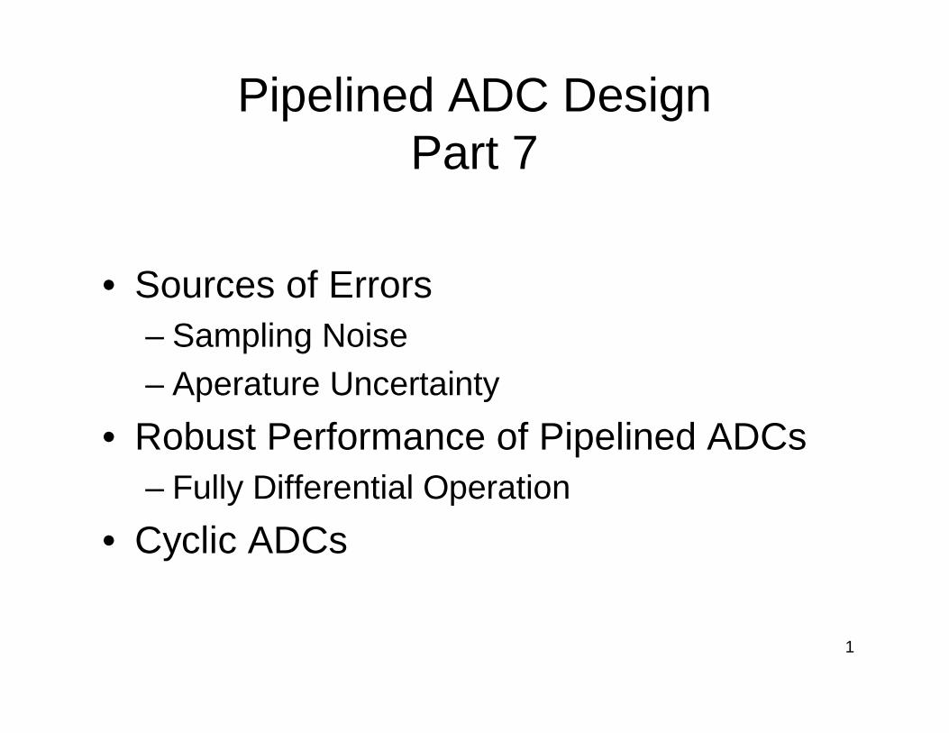
Standard Pipelined ADC Architecture
Amp
dk
XINkXOUTk
CLK
VREF
Review
3
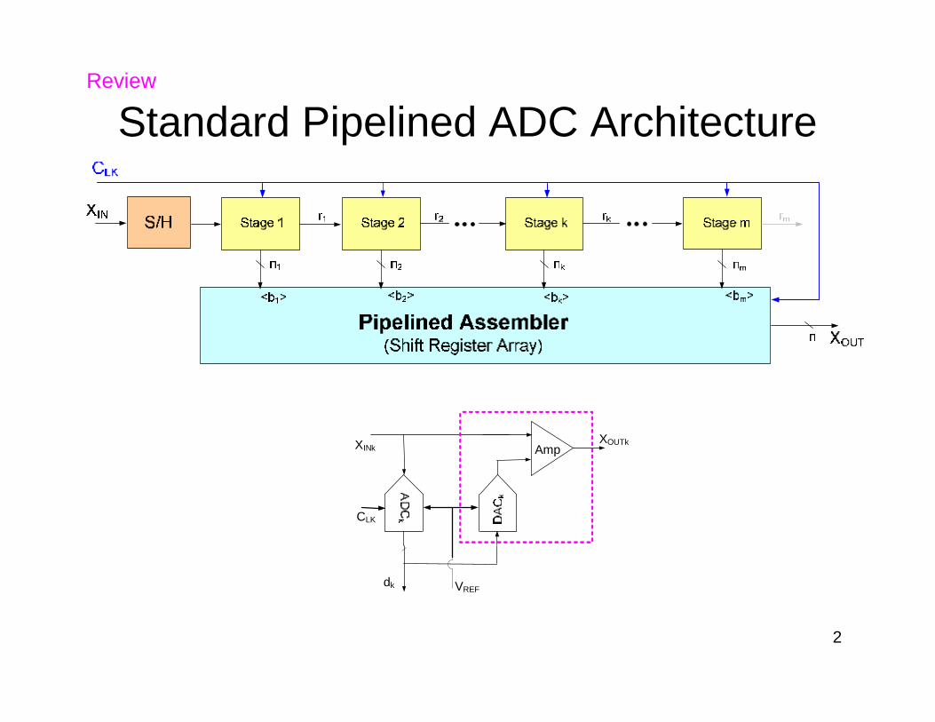
Pseudo-Static Characterization of Pipelined ADC with Arbitrary Bits/Stage
and Out-Range Protectionf(residue)f(offset)dαV
n
1kkkin ++= ∑
=
• the αk are functions of DAC levels and amplifier gains
• f(offset) is code-independent, ideally zero and causes only overall offset error in ADC • f(residue) is code-dependent but can be bounded by 1 lsb(causing at most ½ LSB error) with out-range protection
• dk are boolean output variables from stage ADCs (including out-range protection if included)
• Equation applies to both sub-radix2 and extra comparatorout-range protection
•No errors causing spectral distortion or INL degradation if αk are correctly determined and last residue is variability bounded
Review
•Substantial errors are introduced if ak are not correctly interpreted or f(residue) is not bounded!
4
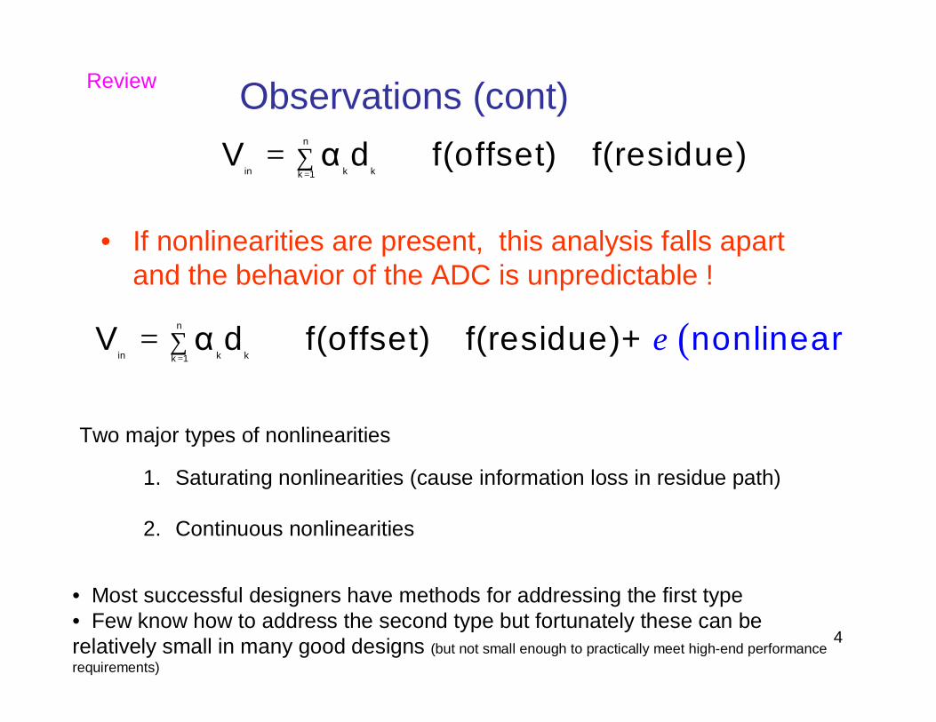
Observations (cont)
• If nonlinearities are present, this analysis falls apart and the behavior of the ADC is unpredictable !
n
in k kk 1V α d f(offset) f(residue)
=∑= + +
Two major types of nonlinearities
1. Saturating nonlinearities (cause information loss in residue path)
2. Continuous nonlinearities
• Most successful designers have methods for addressing the first type• Few know how to address the second type but fortunately these can berelatively small in many good designs (but not small enough to practically meet high-end performance requirements)
( )n
in k kk 1V α d f(offset) f(residue)+ nonlinearε
=∑= + +
Review
5
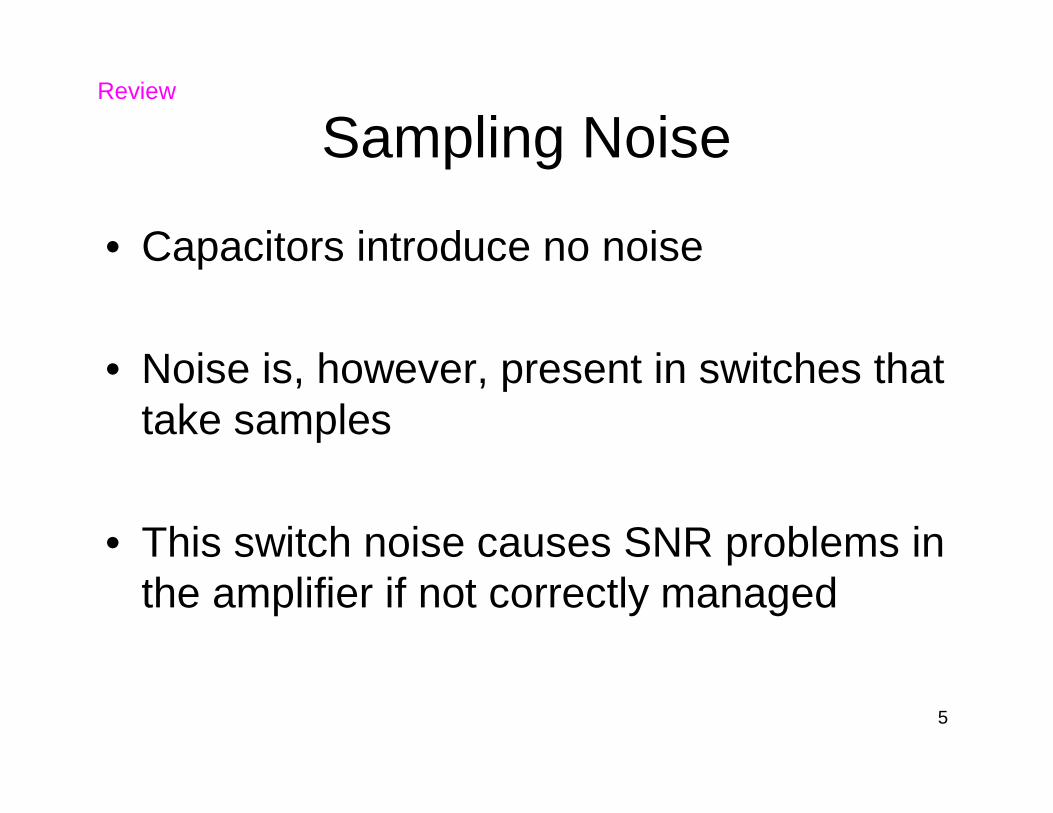
Sampling Noise
• Capacitors introduce no noise
• Noise is, however, present in switches that take samples
• This switch noise causes SNR problems in the amplifier if not correctly managed
Review
6
Sampling Noise
V̂σ
ˆ RMS RMSV
ˆV Vσ = =
ˆRMS RMS V
kTV̂ VC
σ= = =
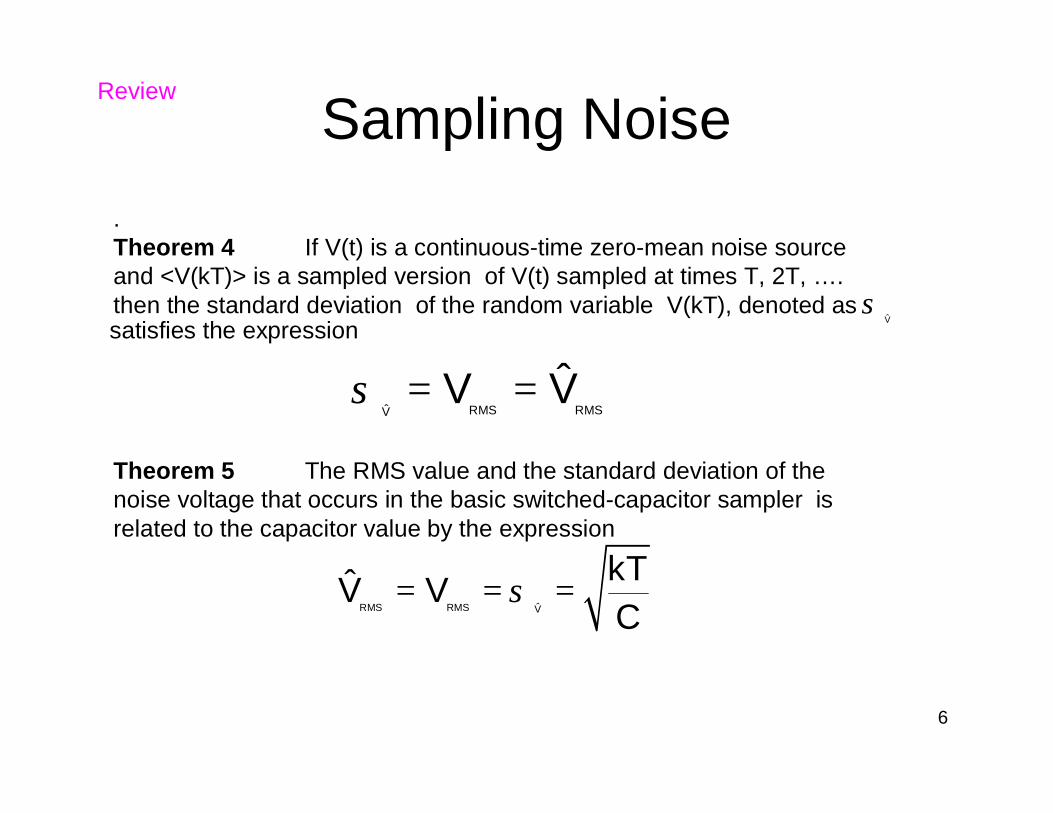
.Theorem 4 If V(t) is a continuous-time zero-mean noise source and <V(kT)> is a sampled version of V(t) sampled at times T, 2T, …. then the standard deviation of the random variable V(kT), denoted as satisfies the expression
Theorem 5 The RMS value and the standard deviation of the noise voltage that occurs in the basic switched-capacitor sampler is related to the capacitor value by the expression
Review
7
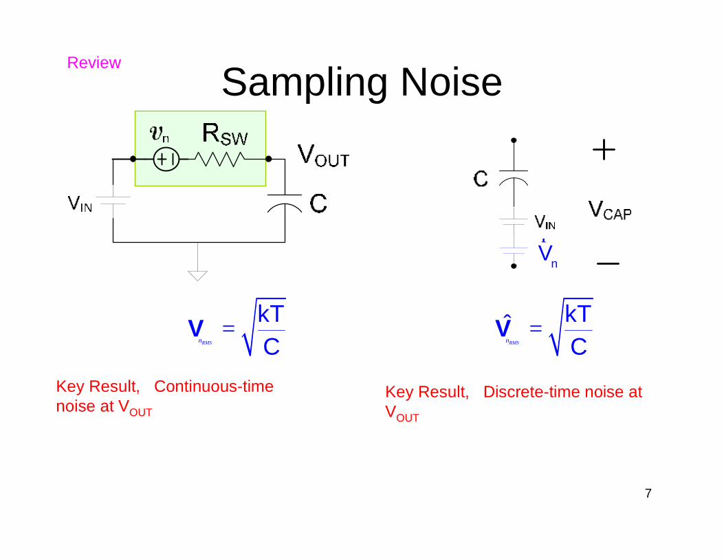
Sampling Noise
kTˆCRMSn
=V
Key Result, Continuous-time noise at VOUT
nVr
kTCRMSn
=V
Key Result, Discrete-time noise at VOUT
Review
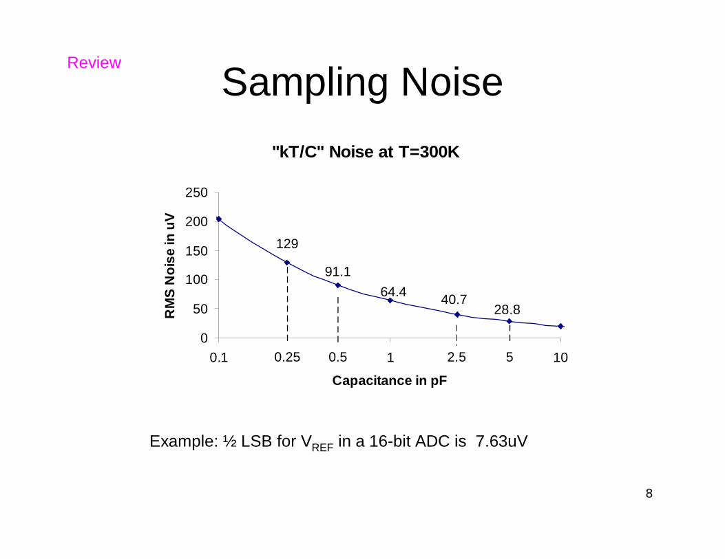
8
Sampling Noise"kT/C" Noise at T=300K
0
50
100
150
200
250
0.1 1 10
Capacitance in pF
RM
S N
oise
in u
V
0.25 2.5 50.5
64.491.1
129
28.840.7
Example: ½ LSB for VREF in a 16-bit ADC is 7.63uV
Review
9
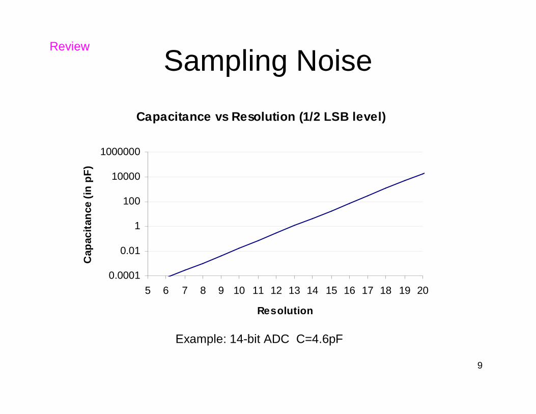
Sampling Noise
Example: 14-bit ADC C=4.6pF
Capacitance vs Resolution (1/2 LSB level)
0.0001
0.01
1
100
10000
1000000
5 6 7 8 9 10 11 12 13 14 15 16 17 18 19 20
Resolution
Cap
acita
nce
(in p
F)
Review
10
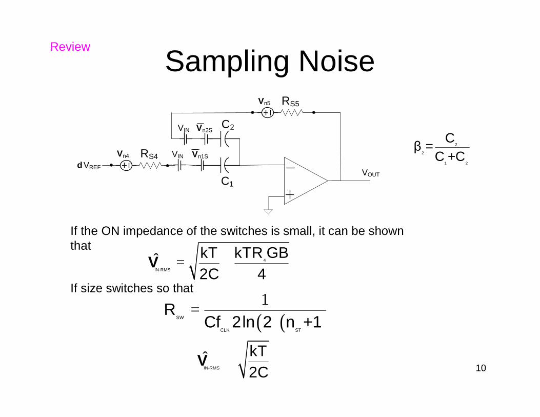
Sampling Noise
C1
C2
VOUTVREFd
RS5Vn5
RS4Vn4 Vn1S
Vn2SVIN
VIN
2
2
1 2
Cβ =C +C
If the ON impedance of the switches is small, it can be shown that
4
IN-RMS
kTR GBkTˆ2C 4
= +V
( )( )1
SW
CLK ST
RCf 2ln 2 n +1
=If size switches so that
IN-RMS
kTˆ2C
≅V
Review
11
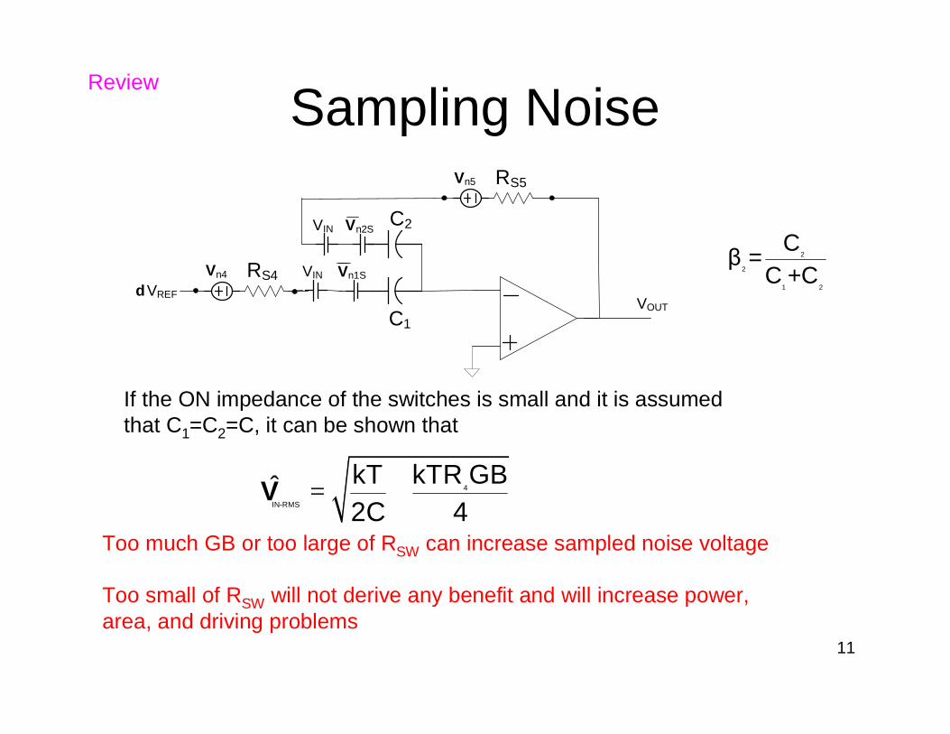
Sampling Noise
C1
C2
VOUTVREFd
RS5Vn5
RS4Vn4 Vn1S
Vn2SVIN
VIN
2
2
1 2
Cβ =C +C
If the ON impedance of the switches is small and it is assumed that C1=C2=C, it can be shown that
4
IN-RMS
kTR GBkTˆ2C 4
= +V
Too much GB or too large of RSW can increase sampled noise voltage
Too small of RSW will not derive any benefit and will increase power, area, and driving problems
Review
12
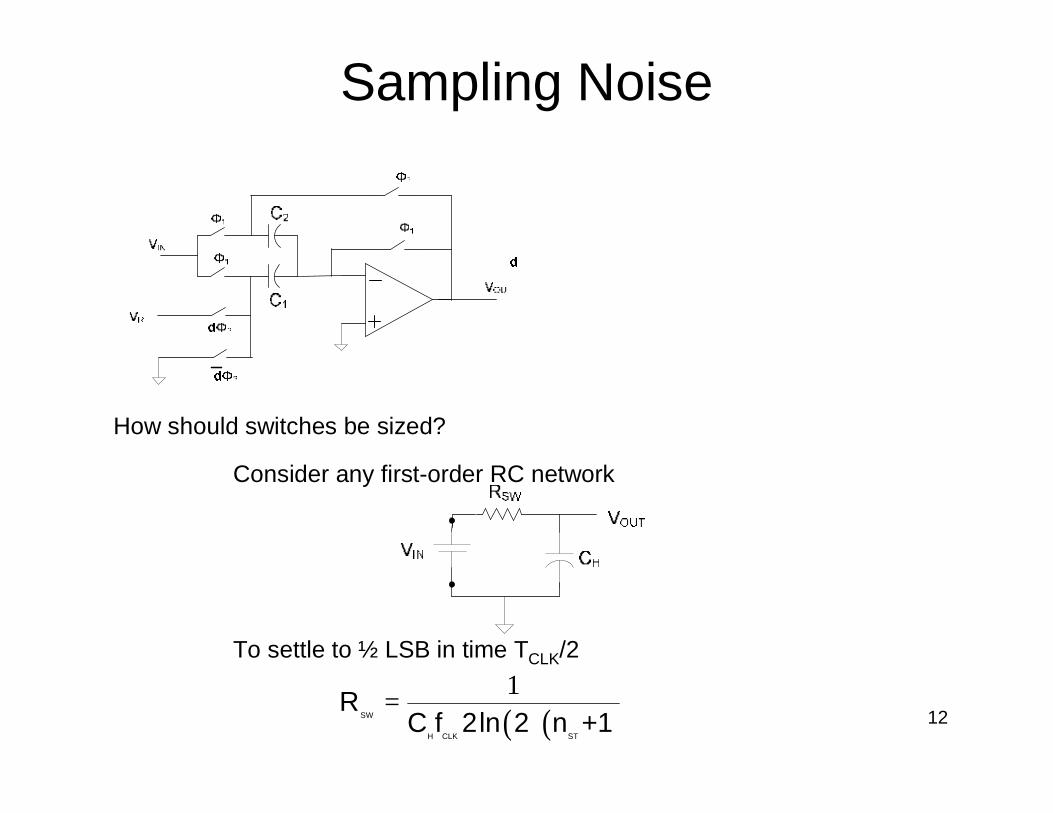
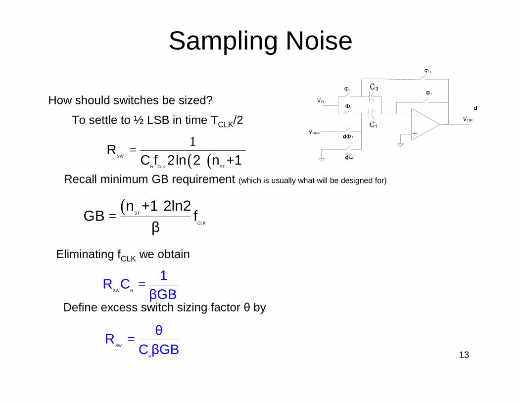
Sampling Noise
( )( )1
SW
H CLK ST
RC f 2ln 2 n +1
=
How should switches be sized?
Consider any first-order RC network
To settle to ½ LSB in time TCLK/2
13
Sampling Noise
( )( )1
SW
H CLK ST
RC f 2ln 2 n +1
=
How should switches be sized?
To settle to ½ LSB in time TCLK/2
( )ST
CLK
n +1 2ln2GB f
β=
Recall minimum GB requirement (which is usually what will be designed for)
Eliminating fCLK we obtain
SW H
1R CβGB
=
Define excess switch sizing factor θ by
SW
H
θRC βGB
=
14
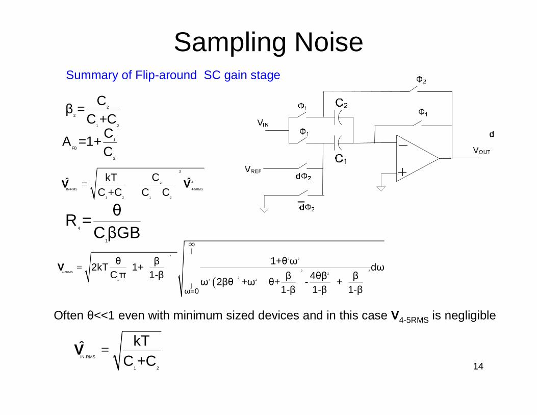
Sampling Noise
2
2
1 2
Cβ =C +C
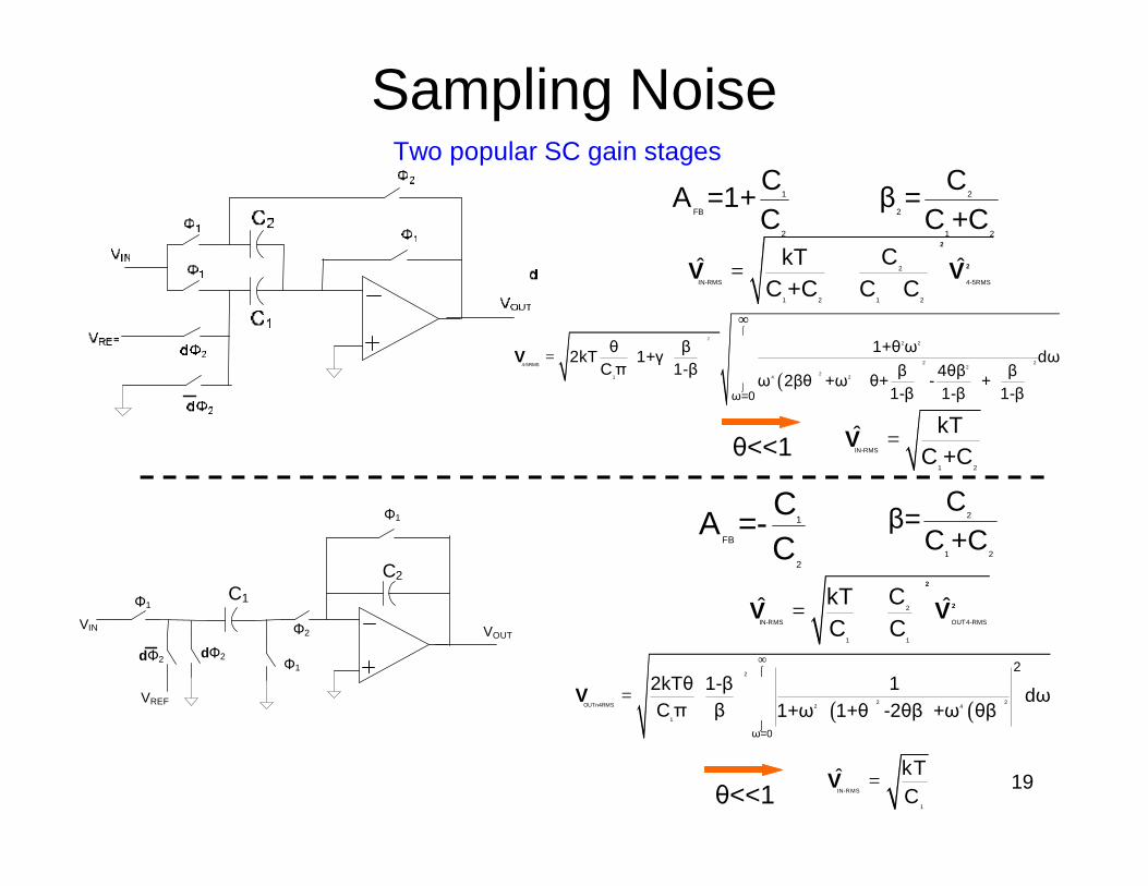
Summary of Flip-around SC gain stage
1
FB
2
CA =1+C
2
IN-RMS 4-5RMS
1 2 1 2
CkTˆ ˆC +C C C
= + +
2
2V V
( )
22 2
2 24-5RMS 22
4 21
ω=0
θ β 1+θ ω2kT 1+ dωCπ 1-β β 4θβ βω 2βθ +ω θ+ - +
1-β 1-β 1-β
⌠⌡
∞
=
V
4
1
θR =CβGB
Often θ<<1 even with minimum sized devices and in this case V4-5RMS is negligible
IN-RMS
1 2
kTˆC +C
=V
15
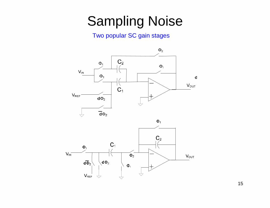
Sampling NoiseTwo popular SC gain stages
16
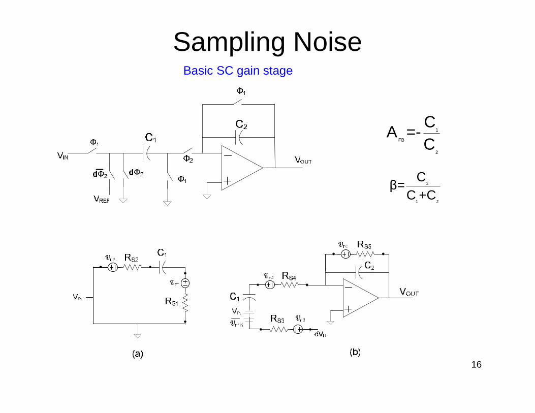
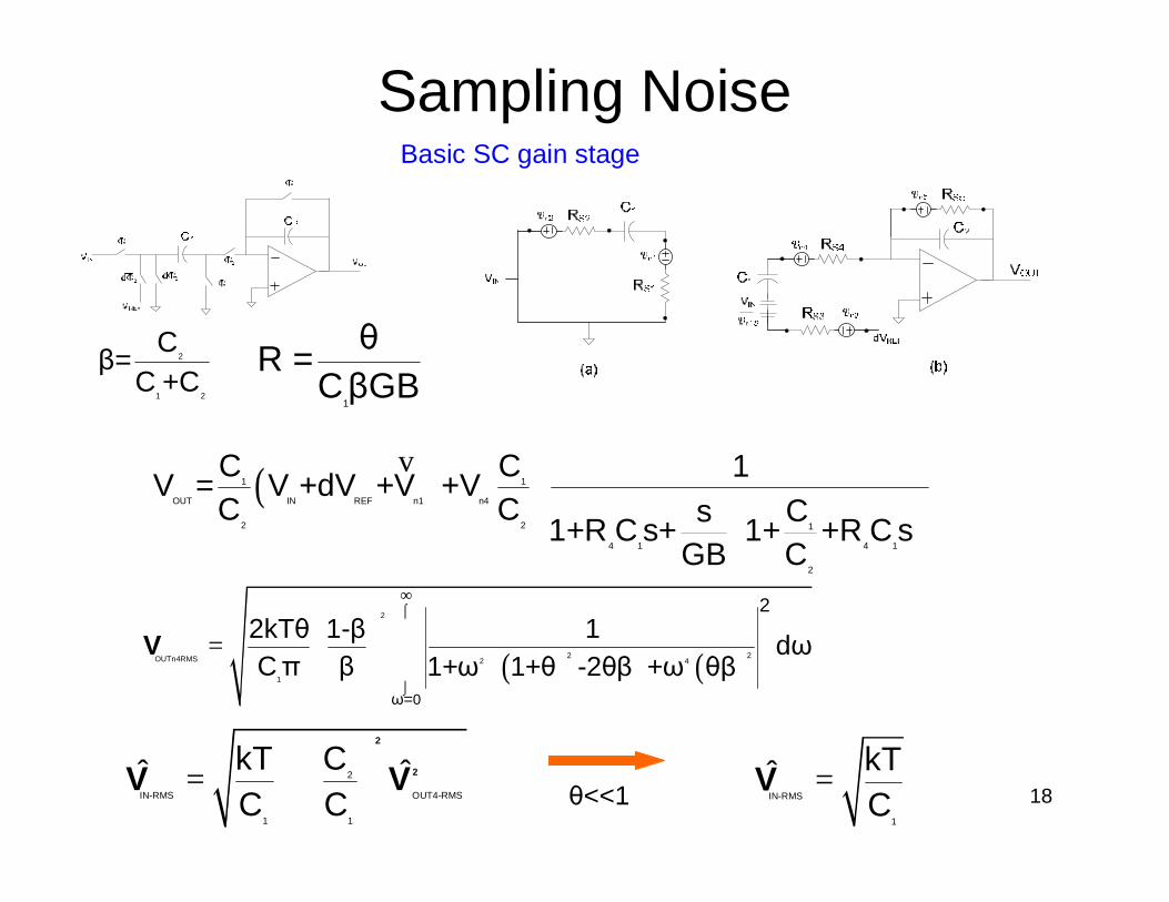
Sampling NoiseBasic SC gain stage
1
FB
2
CA =-C
2
1 2
Cβ=C +C
17
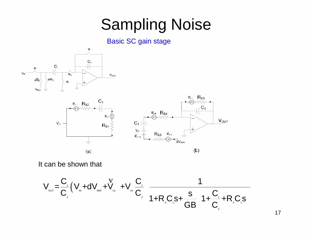
Sampling NoiseBasic SC gain stage
( )1 1
OUT IN REF n1 n4
2 2 1
4 1 4 1
2
C C 1V = V +dV +V +VC C Cs1+R C s+ 1+ +R C s
GB C
v
It can be shown that
18
Sampling NoiseBasic SC gain stage
( )1 1
OUT IN REF n1 n4
2 2 1
4 1 4 1
2
C C 1V = V +dV +V +VC C Cs1+R C s+ 1+ +R C s
GB C
v
2
IN-RMS OUT4-RMS
1 1
CkTˆ ˆC C
= +
2
2V V
( ) ( )
2
2 2OUTn4RMS 2 4
1
0ω=
22kTθ 1-β 1 dωCπ β 1+ω 1+θ -2θβ +ω θβ
⌠⌡
∞
= V
2
1 2
Cβ=C +C
1
θR =CβGB
IN-RMS
1
kTˆC
=Vθ<<1
19
Sampling Noise2
2
1 2
Cβ =C +C
C1
C2
Φ1
Φ1
Φ2VIN VOUT
VREF
dΦ2 dΦ2Φ1
Two popular SC gain stages1
FB
2
CA =1+C
1
FB
2
CA =-C
2
1 2
Cβ=C +C
2
IN-RMS 4-5RMS
1 2 1 2
CkTˆ ˆC +C C C
= + +
2
2V V
( )
22 2
2 24-5RMS 22
4 21
ω=0
θ β 1+θ ω2kT 1+γ dωCπ 1-β β 4θβ βω 2βθ +ω θ+ - +
1-β 1-β 1-β
⌠⌡
∞
=
V
( ) ( )
2
2 2OUTn4RMS 2 4
1
0ω=
22kTθ 1-β 1 dωCπ β 1+ω 1+θ -2θβ +ω θβ
⌠⌡
∞
= V
2
IN-RMS OUT4-RMS
1 1
CkTˆ ˆC C
= +
2
2V V
IN-RMS
1
kTˆC
=Vθ<<1
θ<<1 IN-RMS
1 2
kTˆC +C
=V
20
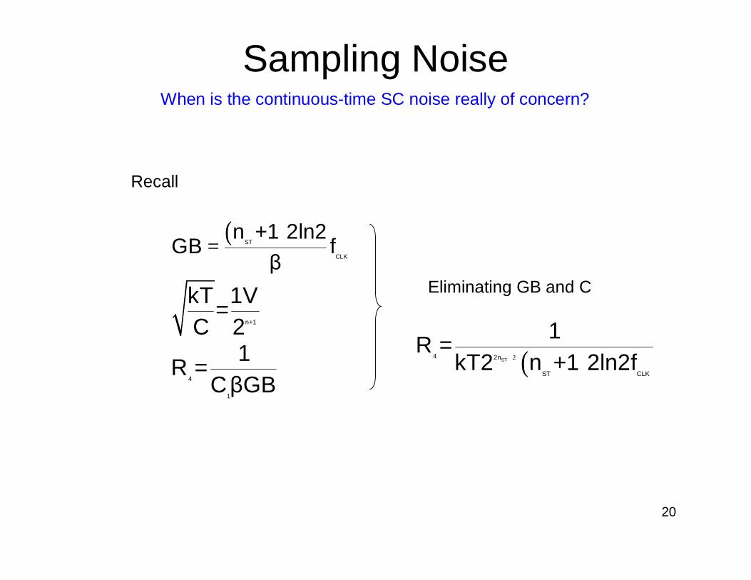
Sampling NoiseWhen is the continuous-time SC noise really of concern?
4
1
1R =CβGB
( )ST
CLK
n +1 2ln2GB f
β=
n+1
kT 1V=C 2
( )2ST4 2n
ST CLK
1R =kT2 n +1 2ln2f+
Eliminating GB and C
Recall
21
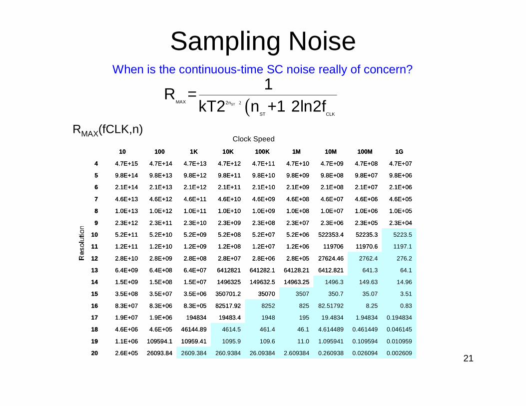
Sampling NoiseWhen is the continuous-time SC noise really of concern?
( )2STMAX 2n
ST CLK
1R =kT2 n +1 2ln2f+
0.0026090.0260940.2609382.60938426.09384260.93842609.38426093.842.6E+0520
0.0109590.1095941.09594111.0109.61095.910959.41109594.11.1E+0619
0.0461450.4614494.61448946.1461.44614.546144.894.6E+054.6E+0618
0.1948341.9483419.4834195194819483.41948341.9E+061.9E+0717
0.838.2582.51792825825282517.928.3E+058.3E+068.3E+0716
3.5135.07350.7350735070350701.23.5E+063.5E+073.5E+0815
14.96149.631496.314963.25149632.514963251.5E+071.5E+081.5E+0914
64.1641.36412.82164128.21641282.164128216.4E+076.4E+086.4E+0913
276.22762.427624.462.8E+052.8E+062.8E+072.8E+082.8E+092.8E+1012
1197.111970.61197061.2E+061.2E+071.2E+081.2E+091.2E+101.2E+1111
5223.552235.3522353.45.2E+065.2E+075.2E+085.2E+095.2E+105.2E+1110
2.3E+042.3E+052.3E+062.3E+072.3E+082.3E+092.3E+102.3E+112.3E+129
1.0E+051.0E+061.0E+071.0E+081.0E+091.0E+101.0E+111.0E+121.0E+138
4.6E+054.6E+064.6E+074.6E+084.6E+094.6E+104.6E+114.6E+124.6E+137
2.1E+062.1E+072.1E+082.1E+092.1E+102.1E+112.1E+122.1E+132.1E+146
9.8E+069.8E+079.8E+089.8E+099.8E+109.8E+119.8E+129.8E+139.8E+145
4.7E+074.7E+084.7E+094.7E+104.7E+114.7E+124.7E+134.7E+144.7E+154
1G100M10M1M100K10K1K10010
Clock SpeedRMAX(fCLK,n)
22
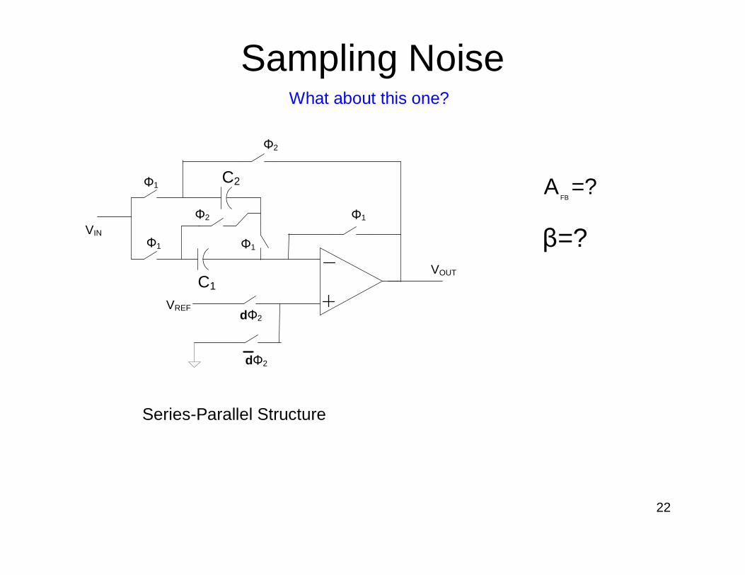
Sampling NoiseWhat about this one?
FBA =?
β=?C1
C2Φ1
Φ1
Φ1
Φ2
VIN
VOUT
VREF dΦ2
dΦ2
Φ1
Φ2
Series-Parallel Structure
23
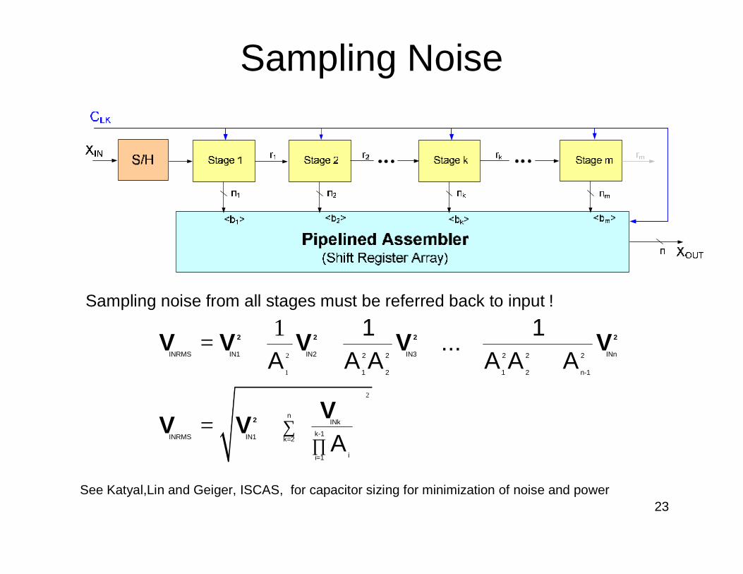
Sampling Noise
Sampling noise from all stages must be referred back to input !
2
1
2
1INRMS IN1 IN2 IN3 INn2 2 2 2 2
1 2 1 2 n-1
nINk
k-1INRMS IN1 k=2
ii=1
1 1...A A A A A A
A∑
∏
= + + + +⋅ ⋅ ⋅
= +
2 2 2 2
2
V V V V V
VV V
See Katyal,Lin and Geiger, ISCAS, for capacitor sizing for minimization of noise and power
24
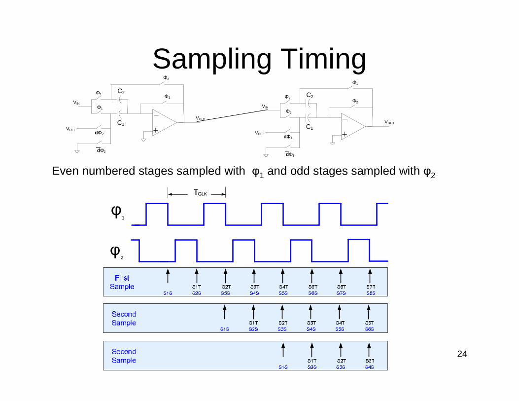
Sampling Timing
C1
C2Φ1
Φ1
Φ1
Φ2
VIN
VOUT
VREF dΦ2
dΦ2
2φ
1φ
C1
C2Φ2
Φ2
Φ1
Φ2VIN
VOUT
VREF dΦ1
dΦ1
Even numbered stages sampled with φ1 and odd stages sampled with φ2
25
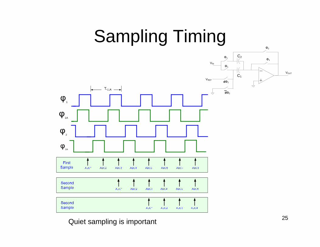
Sampling Timing
C1
C2Φ1
Φ1
Φ1
Φ2
VIN
VOUT
VREF dΦ2
dΦ2
2φ
1φ
1Aφ
2Aφ
Quiet sampling is important
26
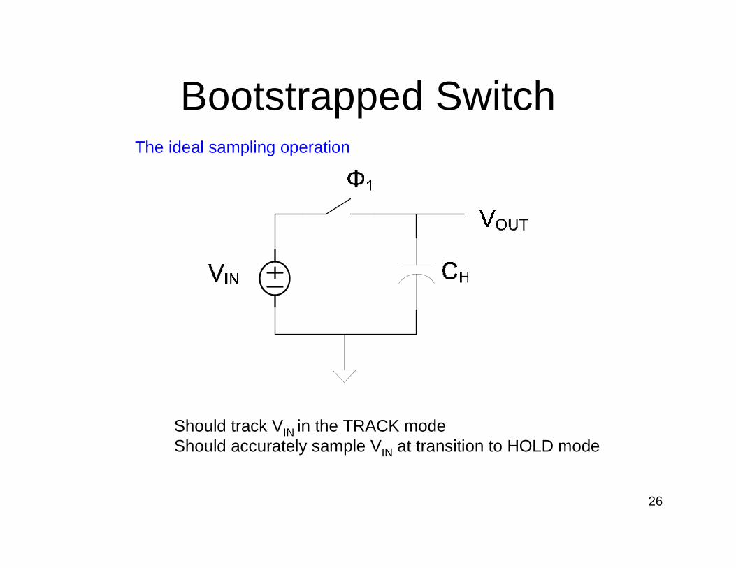
Bootstrapped Switch
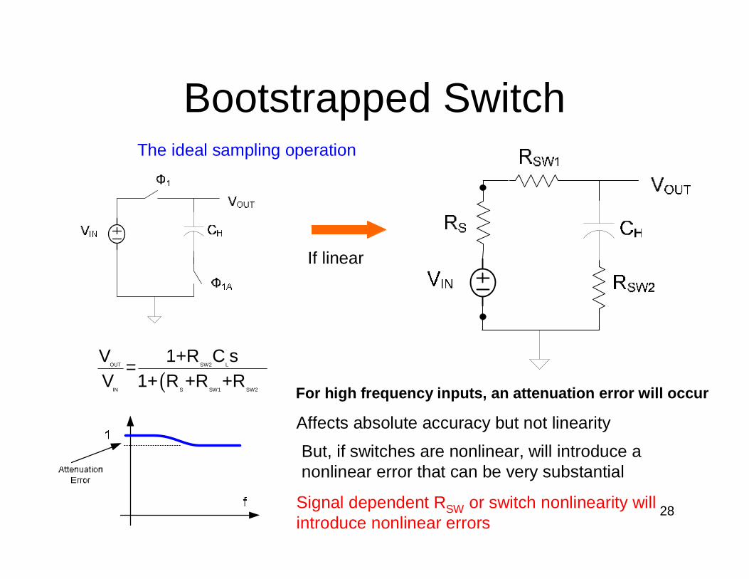
Should track VIN in the TRACK modeShould accurately sample VIN at transition to HOLD mode
The ideal sampling operation
27
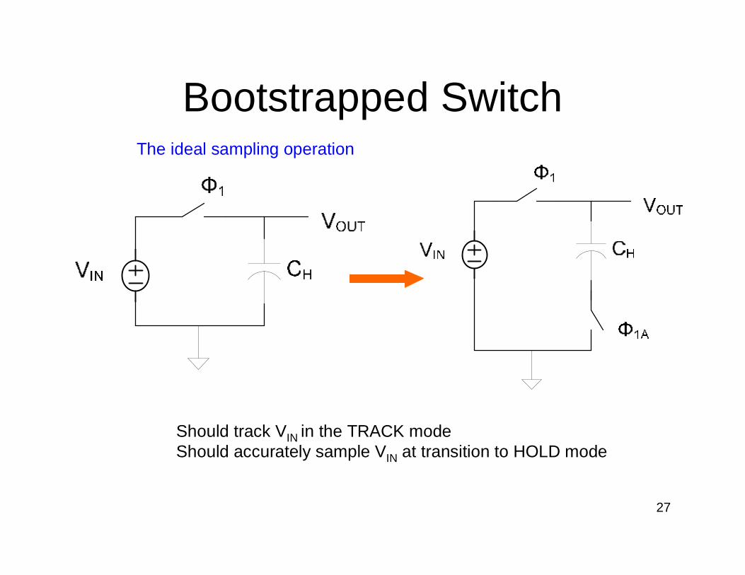
Bootstrapped Switch
Should track VIN in the TRACK modeShould accurately sample VIN at transition to HOLD mode
The ideal sampling operation
28
Bootstrapped SwitchThe ideal sampling operation
( )OUT SW2 L
IN S SW1 SW2
V 1+R C s=V 1+ R +R +R
If linear
For high frequency inputs, an attenuation error will occur
Affects absolute accuracy but not linearity
But, if switches are nonlinear, will introduce a nonlinear error that can be very substantial
Signal dependent RSW or switch nonlinearity will introduce nonlinear errors
29
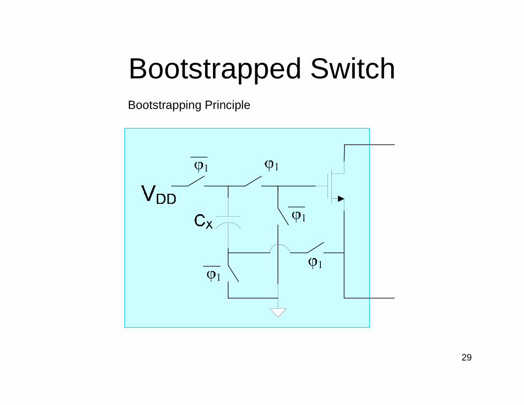
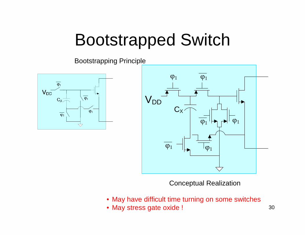
Bootstrapped SwitchBootstrapping Principle
30
Bootstrapped SwitchBootstrapping Principle
Conceptual Realization
• May have difficult time turning on some switches• May stress gate oxide !
VDD
φ1
φ1
φ1
CX
φ1
φ1
φ1
31
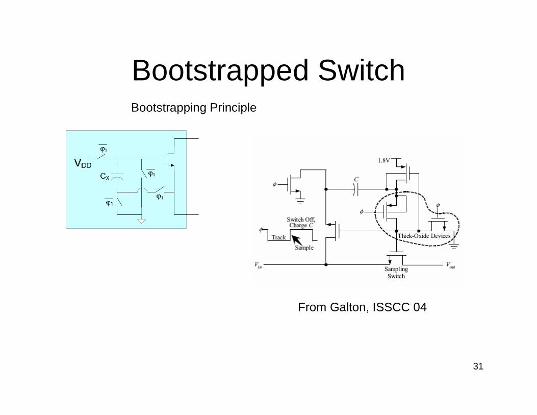
Bootstrapped SwitchBootstrapping Principle
From Galton, ISSCC 04
32
Bootstrapped SwitchBootstrapping Principle
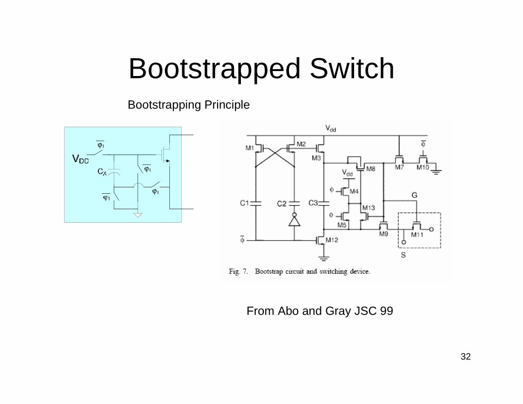
From Abo and Gray JSC 99
33
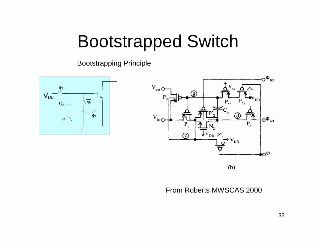
Bootstrapped SwitchBootstrapping Principle
From Roberts MWSCAS 2000
34
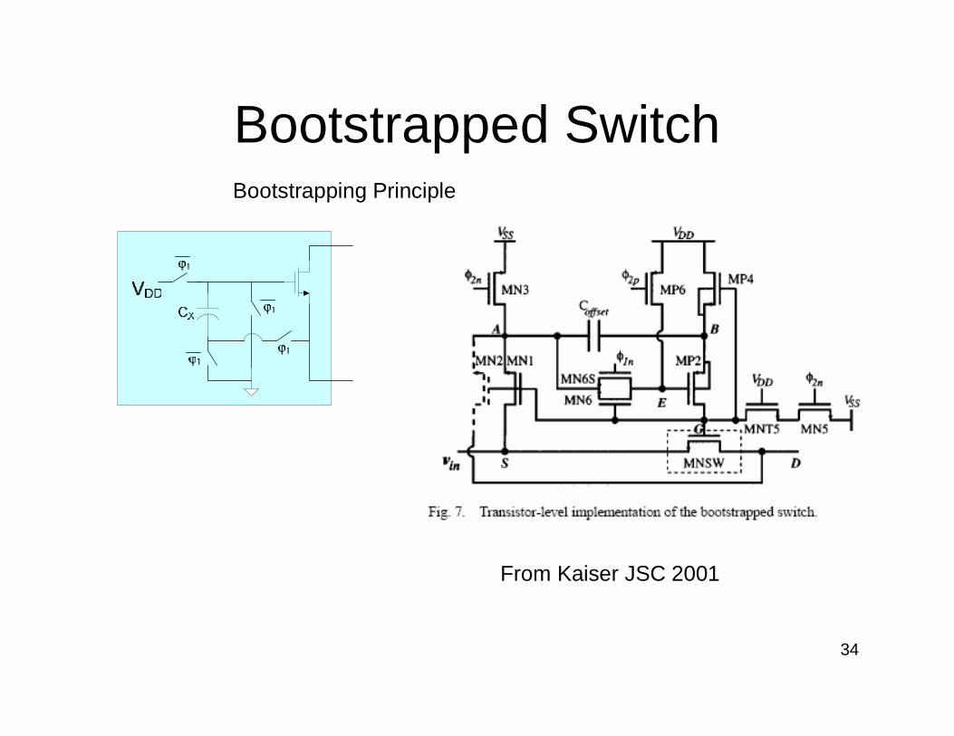
Bootstrapped SwitchBootstrapping Principle
From Kaiser JSC 2001
35
Bootstrapped SwitchBootstrapping Principle
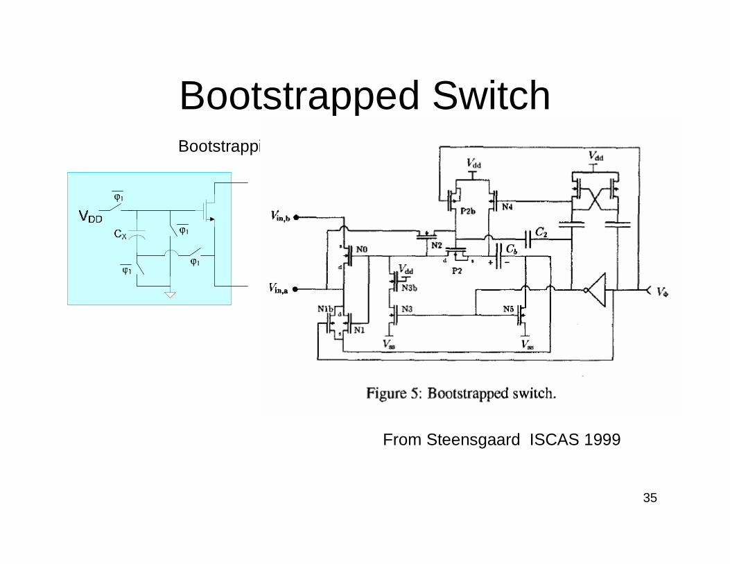
From Steensgaard ISCAS 1999

36
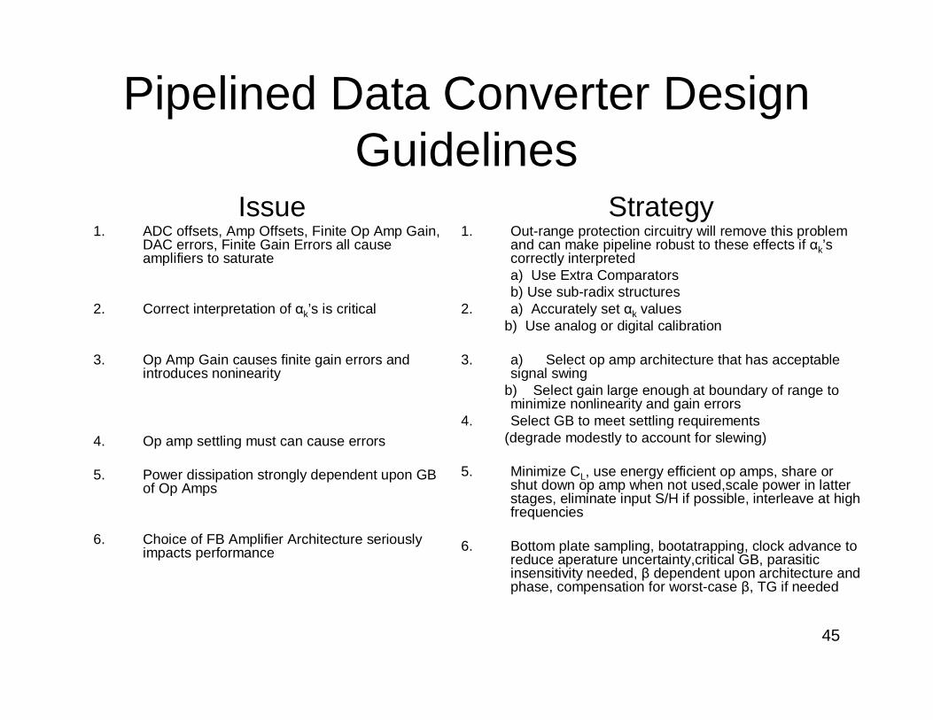
Pipelined Data Converter Design Guidelines
Issue1. ADC offsets, Amp Offsets, Finite Op Amp Gain,
DAC errors, Finite Gain Errors all cause amplifiers to saturate
2. Correct interpretation of αk’s is critical
3. Op Amp Gain causes finite gain errors and introduces noninearity
4. Op amp settling must can cause errors
5. Power dissipation strongly dependent upon GB of Op Amps
6. Choice of FB Amplifier Architecture seriously impacts performance
Strategy1. Out-range protection circuitry will remove this problem
and can make pipeline robust to these effects if αk’scorrectly interpreteda) Use Extra Comparatorsb) Use sub-radix structures
2. a) Accurately set αk valuesb) Use analog or digital calibration
3. a) Select op amp architecture that has acceptable signal swing
b) Select gain large enough at boundary of range to minimize nonlinearity and gain errors
4. Select GB to meet settling requirements(degrade modestly to account for slewing)
5. Minimize CL, use energy efficient op amps, share or shut down op amp when not used,scale power in latter stages, eliminate input S/H if possible, interleave at high frequencies
6. Bottom plate sampling, bootatrapping, clock advance to reduce aperature uncertainty,critical GB, parasitic insensitivity needed, β dependent upon architecture and phase, compensation for worst-case β, TG if needed
37
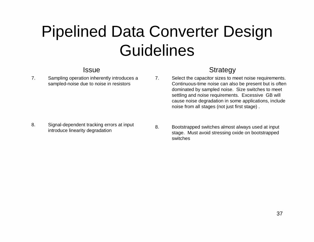
Pipelined Data Converter Design Guidelines
Issue7. Sampling operation inherently introduces a
sampled-noise due to noise in resistors
8. Signal-dependent tracking errors at input introduce linearity degradation
Strategy7. Select the capacitor sizes to meet noise requirements.
Continuous-time noise can also be present but is often dominated by sampled noise. Size switches to meet settling and noise requirements. Excessive GB will cause noise degradation in some applications, include noise from all stages (not just first stage) .
8. Bootstrapped switches almost always used at input stage. Must avoid stressing oxide on bootstrapped switches
38
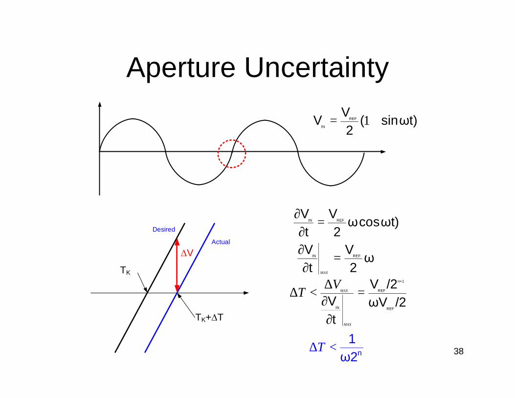
Aperture Uncertainty
TK
TK+∆T
∆VActual
Desired
1REF
IN
VV ( sinωt)2
= +
IN REFV V ωcosωt)t 2
∂=
∂
IN REFV V ωt 2MAX
∂=
∂n+1
REF
IN REF
V /2V ωV /2t
MAX
MAX
VT ∆∆ < =
∂∂
n1
ω2T∆ <
39
Aperture Uncertainty
1REF
IN
VV ( sinωt)2
= +
n1
ω2T∆ <
Example: If fCLK=200MHz, n=14 determine the aperture uncertainty
( )0514
1 4.86E-14 . psec2 2E8 2
Tπ
∆ < = ≅
Aperture uncertainty requirements can be very stringent !
40
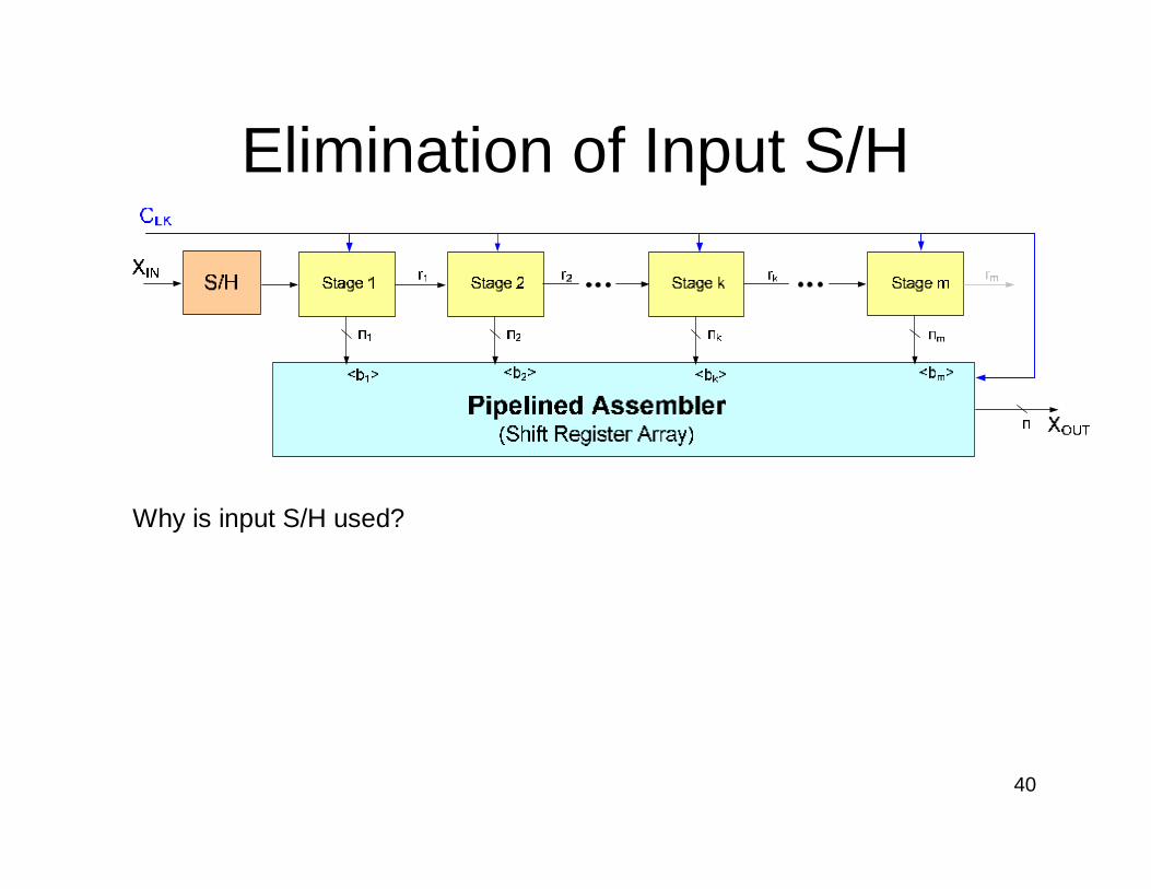
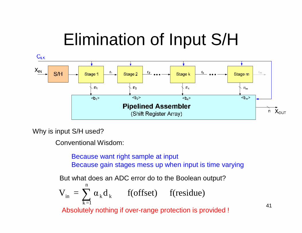
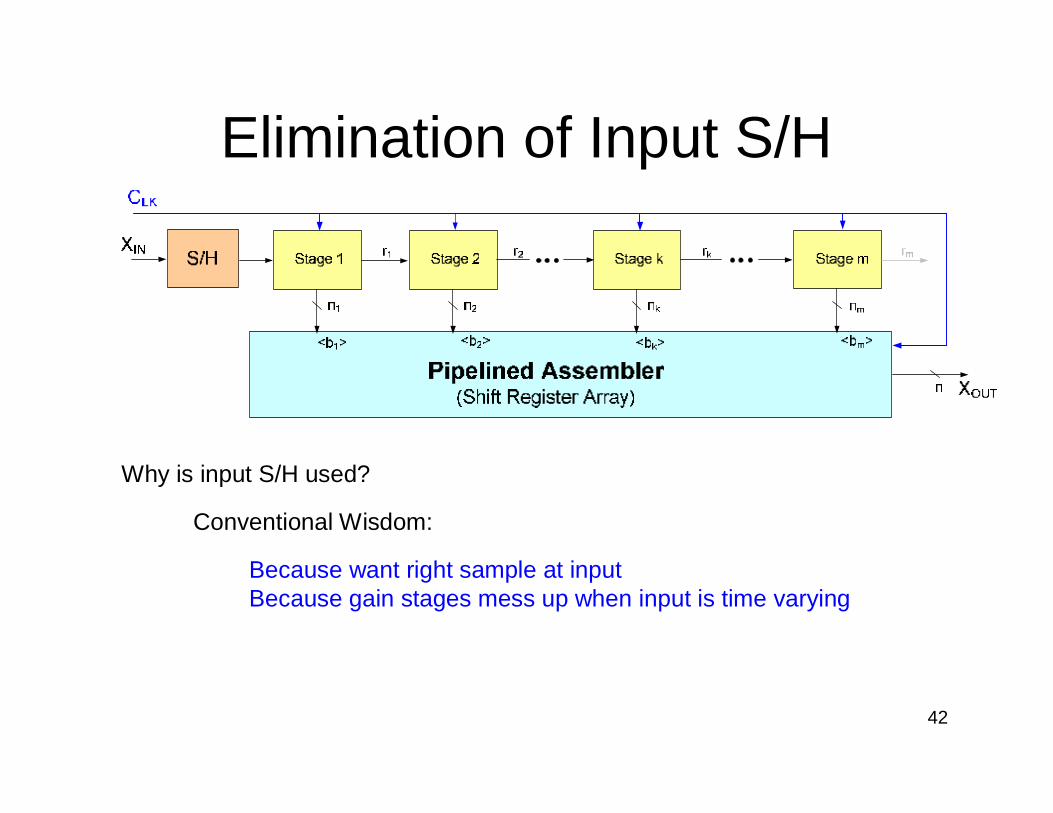
Elimination of Input S/H
Why is input S/H used?
41
Elimination of Input S/H
Why is input S/H used?
Because want right sample at inputBecause gain stages mess up when input is time varying
Conventional Wisdom:
f(residue)f(offset)dαVn
1kkkin ++= ∑
=
But what does an ADC error do to the Boolean output?
Absolutely nothing if over-range protection is provided !
42
Elimination of Input S/H
Why is input S/H used?
Because want right sample at inputBecause gain stages mess up when input is time varying
Conventional Wisdom:
43
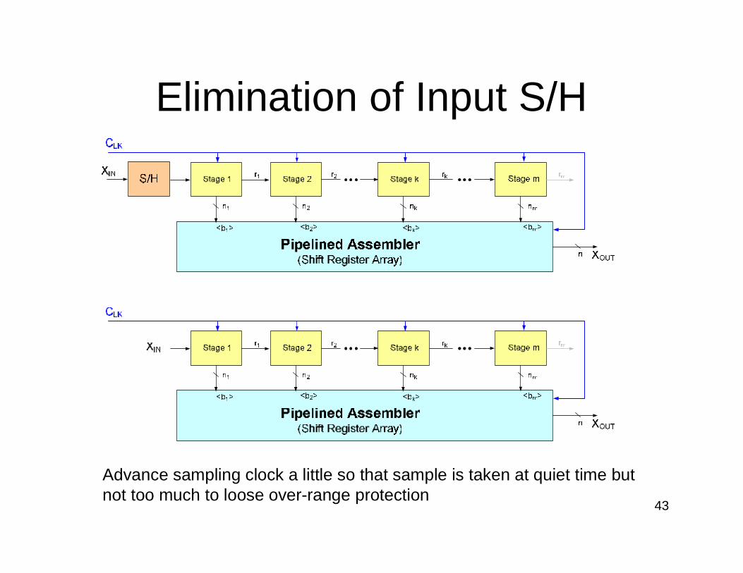
Elimination of Input S/H
Advance sampling clock a little so that sample is taken at quiet time but not too much to loose over-range protection
44
Fully Differential Architectues
• All even-ordered spectral components are eliminated with fully-differential symmetric structures
• Common mode noise is rejected with fully-differential symmetric structures
Second-order spectral component is often most significant contributor to SFDR and THD limitations in single-ended structures
Noise from ADC and other components, coupled through the substrate, often source of considerable noise in an ADC
Almost all implementations of Pipelined ADCs are fully-differential
Straightforward modification of the single-ended concepts discussed here
Authors often present structures in single-ended mode and then just mention that differential structure was used
Modest (but small) increase in area and power for fully differential structures
45
Pipelined Data Converter Design Guidelines
Issue1. ADC offsets, Amp Offsets, Finite Op Amp Gain,
DAC errors, Finite Gain Errors all cause amplifiers to saturate
2. Correct interpretation of αk’s is critical
3. Op Amp Gain causes finite gain errors and introduces noninearity
4. Op amp settling must can cause errors
5. Power dissipation strongly dependent upon GB of Op Amps
6. Choice of FB Amplifier Architecture seriously impacts performance
Strategy1. Out-range protection circuitry will remove this problem
and can make pipeline robust to these effects if αk’scorrectly interpreteda) Use Extra Comparatorsb) Use sub-radix structures
2. a) Accurately set αk valuesb) Use analog or digital calibration
3. a) Select op amp architecture that has acceptable signal swing
b) Select gain large enough at boundary of range to minimize nonlinearity and gain errors
4. Select GB to meet settling requirements(degrade modestly to account for slewing)
5. Minimize CL, use energy efficient op amps, share or shut down op amp when not used,scale power in latter stages, eliminate input S/H if possible, interleave at high frequencies
6. Bottom plate sampling, bootatrapping, clock advance to reduce aperature uncertainty,critical GB, parasitic insensitivity needed, β dependent upon architecture and phase, compensation for worst-case β, TG if needed
46
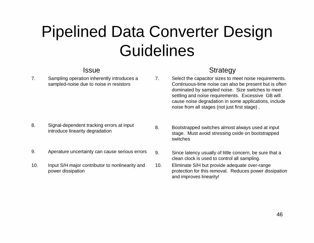
Pipelined Data Converter Design Guidelines
Issue7. Sampling operation inherently introduces a
sampled-noise due to noise in resistors
8. Signal-dependent tracking errors at input introduce linearity degradation
9. Aperature uncertainty can cause serious errors
10. Input S/H major contributor to nonlinearity and power dissipation
Strategy7. Select the capacitor sizes to meet noise requirements.
Continuous-time noise can also be present but is often dominated by sampled noise. Size switches to meet settling and noise requirements. Excessive GB will cause noise degradation in some applications, include noise from all stages (not just first stage) .
8. Bootstrapped switches almost always used at input stage. Must avoid stressing oxide on bootstrapped switches
9. Since latency usually of little concern, be sure that a clean clock is used to control all sampling.
10. Eliminate S/H but provide adequate over-range protection for this removal. Reduces power dissipation and improves linearity!

47
Layout Issues
48
Number of Bits/Stage
49
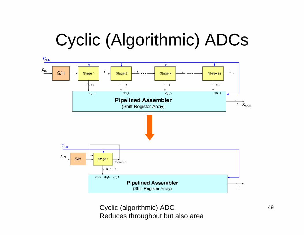
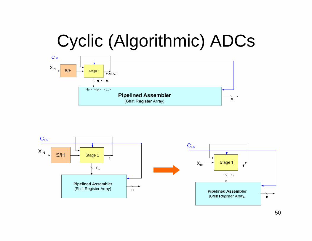
Cyclic (Algorithmic) ADCs
Cyclic (algorithmic) ADCReduces throughput but also area
50
Cyclic (Algorithmic) ADCs
Stage 1
n1
rXIN S/H
nPipelined Assembler (Shift Register Array)
CLK