PIN DIAGRAM -...
53
Transcript of PIN DIAGRAM -...


PIN DIAGRAM
Richa Upadhyay Prabhu
NMIMS’s MPSTME
January 19, 2016
Richa Upadhyay Prabhu (MPSTME) 8080 Microprocessor January 19, 2016 1 / 51
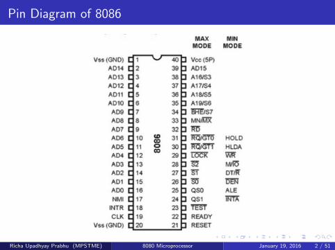
Pin Diagram of 8086
Richa Upadhyay Prabhu (MPSTME) 8080 Microprocessor January 19, 2016 2 / 51

Pin Diagram of 8086
8086 can operate in two modes :
Minimum Mode : unique processor system with a single 8086
Maximum Mode : multiprocessor system with more than one 8086
Richa Upadhyay Prabhu (MPSTME) 8080 Microprocessor January 19, 2016 3 / 51
Richa Upadhyay Prabhu (MPSTME) 8080 Microprocessor January 19, 2016 4 / 51

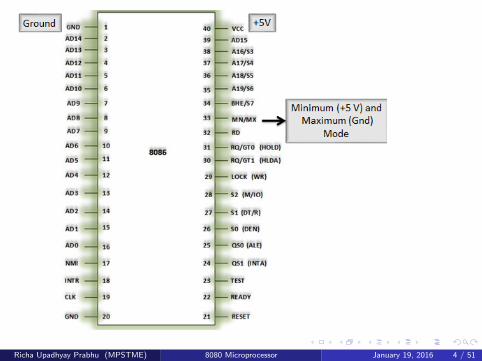
Pin Diagram of 8086
Minimum mode
Pin 33 (MN/MX) connect to +5V
Pin 24-31 are used as memory and I/O control signal
The control signals are generated internally by the 8086/88
Maximum mode
Pin 33 (MN/MX) connect to Ground
Some control signals are generated externally by the 8288 buscontroller chip
Max mode is used when math processor is used.
Richa Upadhyay Prabhu (MPSTME) 8080 Microprocessor January 19, 2016 5 / 51

Richa Upadhyay Prabhu (MPSTME) 8080 Microprocessor January 19, 2016 6 / 51

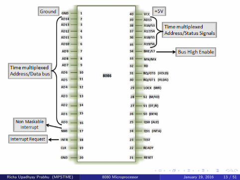
Pin Diagram of 8086
AD15
� AD0 : Address Data Bus
16-bit multiplexed address and data bus
During the 1st clock cycle AD0
� AD15
are the low order 16-Bitaddress
The 8086 has a total of 20 address line ,the upper 4 lines aremultiplexed with the state signal that isA16
/S3
,A17
/S4
,A18
/S5
,A19
/S6
.
During the first clock period the entire 20-bit address is available onthese line
In the next cycle, AD15
� AD0
contain the 16 bit data andS3,S4,S5,S6 become the status line
Richa Upadhyay Prabhu (MPSTME) 8080 Microprocessor January 19, 2016 7 / 51

Pin Diagram of 8086
S3
and S4
are decoded as follows
00 extra segment
01 stack segment
10 code or no segment
11 data segment
After the first clock cycle of an instruction execution, the A17
/S4
andA16
/S3
pins specify which segment register generates the segmentportion of the 8086 address.
Richa Upadhyay Prabhu (MPSTME) 8080 Microprocessor January 19, 2016 8 / 51

Richa Upadhyay Prabhu (MPSTME) 8080 Microprocessor January 19, 2016 9 / 51

BHE/S7
: is used as bus high enable during the 1st clock cycle of aninstruction execution
Used to enable data on the most significant half of data bus
or can say used to distinguish between the low byte and the high byteof the data for the 16-bit external data bus of 8086
BHE is Low during T1 state of read, write and interrupt acknowledgecycles when a byte is to be transferred on the high portion of the bus.
Richa Upadhyay Prabhu (MPSTME) 8080 Microprocessor January 19, 2016 10 / 51

Richa Upadhyay Prabhu (MPSTME) 8080 Microprocessor January 19, 2016 11 / 51
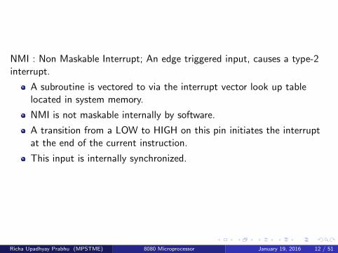
NMI : Non Maskable Interrupt; An edge triggered input, causes a type-2interrupt.
A subroutine is vectored to via the interrupt vector look up tablelocated in system memory.
NMI is not maskable internally by software.
A transition from a LOW to HIGH on this pin initiates the interruptat the end of the current instruction.
This input is internally synchronized.
Richa Upadhyay Prabhu (MPSTME) 8080 Microprocessor January 19, 2016 12 / 51
Richa Upadhyay Prabhu (MPSTME) 8080 Microprocessor January 19, 2016 13 / 51
Pin Diagram of 8086
INTR (Interrupt Request)
An active-high level-triggered input signal to the processor
Sampled in the last clock cycle of each instruction
In IBM PC, this is connected to the 8259 Interrupt controller
Richa Upadhyay Prabhu (MPSTME) 8080 Microprocessor January 19, 2016 14 / 51

Richa Upadhyay Prabhu (MPSTME) 8080 Microprocessor January 19, 2016 15 / 51

Pin Diagram of 8086
RESET : causes the processor to immediately terminate its present activity
Active high signal came from 8284
Force the processor to stop any activities and to discard everything
The signal must be active high for at least four clock cycles,
Data after reset: CS: FFFFH, IP: 0000H, DS ES SS: 0000H Flags:Cleared, Queue: Empty
Richa Upadhyay Prabhu (MPSTME) 8080 Microprocessor January 19, 2016 16 / 51

Richa Upadhyay Prabhu (MPSTME) 8080 Microprocessor January 19, 2016 17 / 51

Generation of Control signals
using RD, WR and IO/M pins
Richa Upadhyay Prabhu (MPSTME) 8080 Microprocessor January 19, 2016 18 / 51

Richa Upadhyay Prabhu (MPSTME) 8080 Microprocessor January 19, 2016 19 / 51

Pin Diagram of 8086
TEST
TEST pin is examined by the ”WAIT” instruction.
If the TEST pin is Low, execution continues. Otherwise the processorwaits in an ”idle” state.
This input is synchronized internally during each clock cycle on theleading edge of CLK.
READY
is the acknowledgement from the addressed memory or I/O devicethat it has completed the data transfer.
The READY signal from memory or I/O is synchronized by the 8284clock generator to form READY.
This signal is active HIGH.
Richa Upadhyay Prabhu (MPSTME) 8080 Microprocessor January 19, 2016 20 / 51

Richa Upadhyay Prabhu (MPSTME) 8080 Microprocessor January 19, 2016 21 / 51

Pin Diagram of 8086
CLOCK (heart beat of CPU)
Clock provides the basic timing for the processor and bus controller.
It is asymmetric with 33 percent duty cycle to provide optimizedinternal timing
Minimum frequency of 5 MHz is required
8284 clock generator chip must be connected to the 8086 clock pin,since it does not have on chip clock generator
The crystal connected to 8284 must have a frequency 3 times the8086 internal frequency
Richa Upadhyay Prabhu (MPSTME) 8080 Microprocessor January 19, 2016 22 / 51

Richa Upadhyay Prabhu (MPSTME) 8080 Microprocessor January 19, 2016 23 / 51

Richa Upadhyay Prabhu (MPSTME) 8080 Microprocessor January 19, 2016 24 / 51

Pin Diagram of 8086
ALE : Address Latch EnableALE is provided by the processor to latch the address into the 8282/8283address latch. It is an active high pulse during T1 of any bus cycle.
DT/ R: DATA Transmit/ReceiveIn minimum mode, 8286/8287 transceiver is used for the data bus. DT/ Ris used to control the direction of data flow through the transceiver.
DEN : Data EnableIt is provided as an output enable for the 8286/8287 in a minimum systemwhich uses the transceiver
Richa Upadhyay Prabhu (MPSTME) 8080 Microprocessor January 19, 2016 25 / 51

Richa Upadhyay Prabhu (MPSTME) 8080 Microprocessor January 19, 2016 26 / 51

Pin Diagram of 8086
HOLD & HLDA (I/O): Hold and Hold Acknowledge
Hold indicates that another master is requesting a local bus ”HOLD”
To be acknowledged, HOLD must be active HIGH.
The processor receiving the ”HOLD ” request will issue HLDA(HIGH) as an acknowledgement in the middle of the T1-clock cycle.
With the issue of HLDA, the processor will float the local bus andcontrol lines
Richa Upadhyay Prabhu (MPSTME) 8080 Microprocessor January 19, 2016 27 / 51

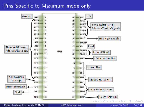
Pins Specific to Maximum mode only
Richa Upadhyay Prabhu (MPSTME) 8080 Microprocessor January 19, 2016 28 / 51
Pin Diagram of 8086
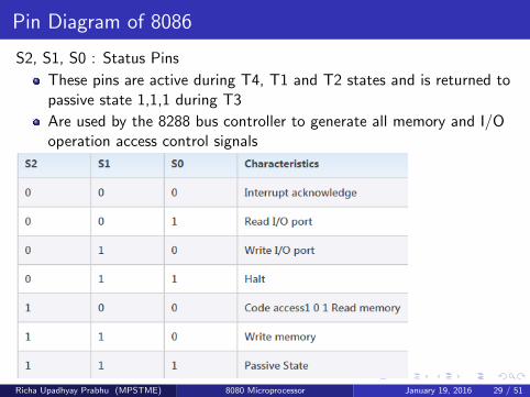
S2, S1, S0 : Status Pins
These pins are active during T4, T1 and T2 states and is returned topassive state 1,1,1 during T3
Are used by the 8288 bus controller to generate all memory and I/Ooperation access control signals
Richa Upadhyay Prabhu (MPSTME) 8080 Microprocessor January 19, 2016 29 / 51

Pins Specific to Maximum mode only
Richa Upadhyay Prabhu (MPSTME) 8080 Microprocessor January 19, 2016 30 / 51

Pin Diagram of 8086
QS0, QS1: Queue Status
Queue Status is valid during the clock cycle after which the queueoperation is performed
QS0, QS1 provide status to allow external tracking of the internal8086 instruction queue
Richa Upadhyay Prabhu (MPSTME) 8080 Microprocessor January 19, 2016 31 / 51

Pins Specific to Maximum mode only
Richa Upadhyay Prabhu (MPSTME) 8080 Microprocessor January 19, 2016 32 / 51

Pin Diagram of 8086
LOCK
It indicates to another system bus master, not to gain control of thesystem bus while LOCK is active Low
The LOCK signal is activated by the ”LOCK” prefix instruction andremains active until the completion of the instruction
This signal is active Low and floats to tri-state OFF during ’holdacknowledge’
Richa Upadhyay Prabhu (MPSTME) 8080 Microprocessor January 19, 2016 33 / 51
Pins Specific to Maximum mode only
Richa Upadhyay Prabhu (MPSTME) 8080 Microprocessor January 19, 2016 34 / 51

Pin Diagram of 8086
RQ/GT0 and RQ/GT1 (I/O): Request/Grant
Are used by other processors in a multi processor organization
Local bus masters of other processors force the processor to releasethe local bus at the end of the processors current bus cycle
Each pin is bi-directional and has an internal pull up resistors. Hencethey may be left un-connected
Richa Upadhyay Prabhu (MPSTME) 8080 Microprocessor January 19, 2016 35 / 51

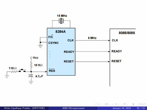
8284 CLOCK GENERATOR
Ancillary component to the 8086/8088 microprocessors
The 8284 provides the following basic functions or signals:Clock generation (CLK)RESET synchronizationREADY synchronizationTTL level peripheral clock (PCLK)
Richa Upadhyay Prabhu (MPSTME) 8080 Microprocessor January 19, 2016 36 / 51

8284 CLOCK GENERATOR
The 8088/8086 require a specific waveform for the system clock
Fast rise and fall times ( ¡10ns )
Logic 0: -0.5 to 0.6 V
Logic 1: 3.9 to 5.0 V
Duty cycle of 33
33% duty cycle
Richa Upadhyay Prabhu (MPSTME) 8080 Microprocessor January 19, 2016 37 / 51

8284 CLOCK GENERATOR
Richa Upadhyay Prabhu (MPSTME) 8080 Microprocessor January 19, 2016 38 / 51

8284 CLOCK GENERATOR
Input Pins
RES (ResetIn): from power supplier
X1 and X2 (Crystal In):the crystal frequency must be3 times the desired frequencyfor the microprocessor
RDY1 and AEN1: providea Ready signal to processor,which will insert a WAIT stateto the CPU read/write cycle
RDY2 and AEN2:For multiprocessor systems
Richa Upadhyay Prabhu (MPSTME) 8080 Microprocessor January 19, 2016 39 / 51

8284 CLOCK GENERATOR
Output Pins
RESET: reset signal to the8086/88, activated by RES
OSC (oscillator):provide to the expansion slot
CLK (clock):1/3 of the crystal input,with a duty cycle of 33%
PCLK: one-half of CLK (1/6of crystal) with duty cycle of50% and is TTL compatible.
READY:connect to READY inputof CPU to insert WAIT state
Richa Upadhyay Prabhu (MPSTME) 8080 Microprocessor January 19, 2016 40 / 51

8284 CLOCK GENERATOR
Output PinsF/C (Frequency/crystalselect): If 1, an externalclock is provided to the EFIinput pin and if 0, an externalcrystal oscillator connected toX1 and X2 provides the clockEFI (External frequencyInput ): Supplies the timingwhenever the F/C is high.CSYNC(Clock Synchronization):Used whenever the EFIinput provides synchronizationin systems with multipleprocessors. If the internalcrystal oscillator is used,this pin must be grounded.Richa Upadhyay Prabhu (MPSTME) 8080 Microprocessor January 19, 2016 41 / 51
Richa Upadhyay Prabhu (MPSTME) 8080 Microprocessor January 19, 2016 42 / 51

8282/8283 LATCH
Richa Upadhyay Prabhu (MPSTME) 8080 Microprocessor January 19, 2016 43 / 51

8282/8283 LATCH
CMOS octal latching bu↵er
provides an eight bit parallel latch/bu↵er in a 20 pin package
Basically de-multiplexing the data and addressing bus
OE (Output Enable) connected to GND, the chip is selected
STB (Strobe) is connected to the pin ALE (Address Latch Enable) ofthe processor and takes over the address data from the multiplexedaddress-/databus
Latches are used to de-multiplex the address/data and address/status lines and
commonly have output bu↵ers for driving external loads.
Richa Upadhyay Prabhu (MPSTME) 8080 Microprocessor January 19, 2016 44 / 51
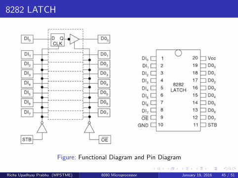
8282 LATCH
Figure: Functional Diagram and Pin Diagram
Richa Upadhyay Prabhu (MPSTME) 8080 Microprocessor January 19, 2016 45 / 51
8286 TRANSCEIVER
Richa Upadhyay Prabhu (MPSTME) 8080 Microprocessor January 19, 2016 46 / 51
8286 TRANSCEIVER
If a system includes several interfaces then to increase currentsourcing/sinking capacities it is necessary to use drivers and receiversfor data bus also
Intel 8286 device is used to implement the transceiver block
Richa Upadhyay Prabhu (MPSTME) 8080 Microprocessor January 19, 2016 47 / 51

Richa Upadhyay Prabhu (MPSTME) 8080 Microprocessor January 19, 2016 48 / 51

8286 TRANSCEIVER
If a system includes several interfaces then to increase currentsourcing/sinking capacities it is necessary to use drivers and receiversfor data bus also
Intel 8286 device is used to implement the transceiver block
It has 16- tri state elements, 8 receivers and 8 drivers
That’s why TWO 8286 are required to service 16 data lines of 8086
DT/R is connected to T input, which controls the direction of dataflow
Richa Upadhyay Prabhu (MPSTME) 8080 Microprocessor January 19, 2016 49 / 51

8286 TRANSCEIVER
DT/R is connected to T input, which controls the direction of dataflow
When this signal is low, receivers are enabled, so that 8086 can readdata from memory and I/O deviceWhen this signal goes high, drivers are enabled allowing 8086 totransfer(or write) data into memory and I/O device
To enable output of transceiver its OE pin should be low, That’s whyit is connected to DEN pin of 8086.
Since DEN signal goes low when CPU is ready to send or receive data
Richa Upadhyay Prabhu (MPSTME) 8080 Microprocessor January 19, 2016 50 / 51
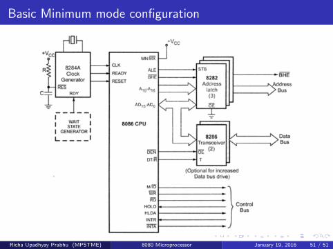
Basic Minimum mode configuration
Richa Upadhyay Prabhu (MPSTME) 8080 Microprocessor January 19, 2016 51 / 51