PIL AMS-APD/12/7659 Dated 27 Dec 2012 - Farnell element14PIL AMS-APD/12/7659 - Dated 27 Dec 2012...
25
PIL AMS-APD/12/7659 Dated 27 Dec 2012 Production line extension within ST Ang Mo Kio (Singapore) for AMS Group products 1/25 PRODUCT INFORMATION LETTER ®
Transcript of PIL AMS-APD/12/7659 Dated 27 Dec 2012 - Farnell element14PIL AMS-APD/12/7659 - Dated 27 Dec 2012...

PIL AMS-APD/12/7659Dated 27 Dec 2012
Production line extension within ST Ang Mo Kio
(Singapore) for AMS Group products
1/25
PRODUCT INFORMATIONLETTER®

PIL AMS-APD/12/7659 - Dated 27 Dec 2012
Sales Type/product family label See here attached
Type of change Waferfab additional location
Reason for change Production capacity increase
Description Progressing on the activities related to JFet diffusion manufacturingprocesses, ST is glad to announce line extension, for AMS productsproduced in JFet process within the same ST plant Ang Mo Kio inSingapore.
Forecasted date of implementation 20-Dec-2012
Forecasted date of samples for customer 20-Dec-2012
Forecasted date for STMicroelectronicschange Qualification Plan results availability 20-Dec-2012
Involved ST facilities ST Ang Mo Kio in Singapore
® 2/25

PIL AMS-APD/12/7659 - Dated 27 Dec 2012
DOCUMENT APPROVAL
Name Function
Camiolo, Jean Marketing Manager
De marco, Alberto Product Manager
Bugnard, Jean-Marc Q.A. Manager
® 3/25

19-12-2012 QF212JV1
Error! Unknown document property name. Page 1/21
PRODUCT/PROCESS CHANGE NOTIFICATION
PIL AMS-APD/12/7659
Analog, MEMS and Sensor Group
Line extension for JFET production in ST Singapore for AMS products

19-12-2012 QF212JV1
Error! Unknown document property name. Page 2/21
WHAT: Progressing on the activities related to bipolar diffusion manufacturing processes, ST is glad to announce line extension, for AMS products produced in Jfet process.
Material
Current process
JFET
Modified process
JFET
Diffusion location ST Singapore ST Singapore
Building AMK6 AMJ9 Facilities No change
Equipments type No Change
Material No change
For the complete list of the part numbers affected by the change, please refer to the attached Products list. WHY: To increase our production capacity for bipolar process in ST Singapore. HOW: The change that covers AMS products is already qualified through attached report. Here below you’ll find the details of qualification plan. Qualification program and results: The qualification program consists mainly of comparative electrical characterization and reliability tests. Please refer to Appendix 1 for all the details. WHEN: Production in ST Singapore AMJ9 for AMS is already started. Marking and traceability: Unless otherwise stated by customer specific requirement, the traceability of the parts assembled with the new material set will be ensured by new internal sales types. The changes here reported will not affect the electrical, dimensional and thermal parameters keeping unchanged all information reported on the relevant datasheets. There is as well no change in the packing process or in the standard delivery quantities.
19-12-2012 QF212JV1
Error! Unknown document property name. Page 3/21
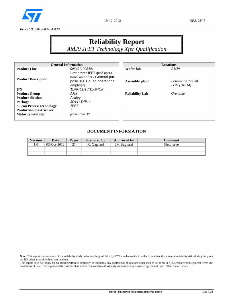
Report ID 2012-W40 AMJ9
Reliability Report AMJ9 JFET Technology Xfer Qualification
General Information Product Line 006401, 008401
Product Description
Low power JFET quad opera-tional amplifier / General pur-pose JFET quad operational amplifiers
P/N TL064CDT / TL084CN Product Group AMS Product division Analog Package SO14 / DIP14 Silicon Process technology JFET Production mask set rev. 1 Maturity level step from 10 to 30
Locations Wafer fab AMJ9 Assembly plant Bouskoura (SO14) LGG (DIP14) Reliability Lab Grenoble
DOCUMENT INFORMATION
Version Date Pages Prepared by Approved by Comment 1.0 03-Oct-2012 21 X. Gagnard JM Bugnard First issue
Note: This report is a summary of the reliability trials performed in good faith by STMicroelectronics in order to evaluate the potential reliability risks during the prod-uct life using a set of defined test methods. This report does not imply for STMicroelectronics expressly or implicitly any contractual obligations other than as set forth in STMicroelectronics general terms and conditions of Sale. This report and its contents shall not be disclosed to a third party without previous written agreement from STMicroelectronics.

19-12-2012 QF212JV1
Error! Unknown document property name. Page 4/21
TABLE OF CONTENTS 1 APPLICABLE AND REFERENCE DOCUMENTS ............................................................................................ 5
2 GLOSSARY ........................................................................................................................................................ 5
3 RELIABILITY EVALUATION OVERVIEW ......................................................................................................... 5
3.1 OBJECTIVES ............................................................................................................................................... 5
3.2 CONCLUSION .............................................................................................................................................. 5
4 DEVICE CHARACTERISTICS ........................................................................................................................... 6
4.1 DEVICE DESCRIPTION .................................................................................................................................. 6
4.2 CONSTRUCTION NOTE ................................................................................................................................. 8
5 TESTS RESULTS SUMMARY ........................................................................................................................... 9
5.1 TEST VEHICLE ............................................................................................................................................. 9
5.2 TEST PLAN AND RESULTS SUMMARY ............................................................................................................. 9
6 ANNEXES ......................................................................................................................................................... 10
6.1 DEVICE DETAILS ........................................................................................................................................ 10
6.2 TESTS DESCRIPTION ................................................................................................................................. 17
6.3 ESD CERTIFICATES ................................................................................................................................... 18
6.4 LU CERTIFICATES ..................................................................................................................................... 20

December 2012 5
1 APPLICABLE AND REFERENCE DOCUMENTS
Document reference Short description AEC-Q100 Stress test qualification for automotive grade integrated circuits AEC-Q101 Stress test qualification for automotive grade discrete semiconductors JESD47 Stress-Test-Driven Qualification of Integrated Circuits
2 GLOSSARY DUT Device Under Test PCB Printed Circuit Board SS Sample Size
3 RELIABILITY EVALUATION OVERVIEW
3.1 Objectives The objective of this qualification is the transfer of the BIPOLAR/JFET technology in 6 inches, from AMK6 to AMJ9. The transfer is based in a copy paste transfer of the equipments and the recipes. In term of building the AMJ9 is located in the AMK5 building, but using the same informatics tracking systems than AMK6, the same facilities, and the same management of documentations & process control. The qualification is using 2 tests vehicles in PRO and 2 tests vehicles in JFET. The qualification of AMJ9 is also based on 0431 product qualified by IPC/APM. This report concerns only the JFET/BIPOLAR technology, the PRO/BIPOLAR being already qualified.
3.2 Conclusion
Qualification Plan requirements have been fulfilled without exception. It is stressed that reliability tests have shown that the devices behave correctly against environmental tests (no failure). Moreover, the stability of electrical parameters during the accelerated tests demonstrates the ruggedness of the products and safe operation, which is consequently expected during their lifetime.

PIL AMS-APD/12/7659
6
4 DEVICE CHARACTERISTICS
4.1 Device description

PIL AMS-APD/12/7659
7

PIL AMS-APD/12/7659
8
4.2 Construction note Site AMJ9 P/N TL064CDT P/N TL084CN
Wafer/Die fab. information Wafer fab manufacturing location AMJ9 Technology JFET Process family JFET421A Die finishing back side Raw silicon Die size 2940 x 1520 µm² 2480 x 1460 µm² Bond pad metallization layers AlSiCu Passivation type PVAPOX/SiN Poly silicon layers NA Wafer Testing (EWS) information Electrical testing manufacturing location Singapore Tester AOT Not yet defined Test program H0064CW.01 Not yet defined Assembly information Assembly site BSK LGG Package description SO14 DIP14 Molding compound EME-G700K GR360A-ST Frame material Cu Cu Die attach process Glue Glue Die attach material 8601S-25 8390S25 Die pad size 132 x 132 µm² 81 x 81 µm² Wire bonding process Wire Wire Wires bonding materials/diameters Cu 1 mil Cu 1 mil Lead finishing process Pre plated Plating Lead finishing/bump solder material NiPdAu Sn Substrate supplier for BGA NA NA Final testing information Testing location BSK LGG Tester ASL1000 ASL1000 Test program T0064AF4 T0084AF5

PIL AMS-APD/12/7659
9
5 TESTS RESULTS SUMMARY
5.1 Test vehicle Lot
# Diffusion
Lot Assy Lot Trace Code Process/ Package Product Line Comments
1 W212NK7 CA1221N140 CZ2250EU SO14 006401 TL064CDT$DFWH 2 W129NTJ 0084QLAMJ9 G4145088 DIP14 008401 TL084CN$LIW 3
Detailed results in below chapter will refer to P/N and Lot #.
5.2 Test plan and results summary P/N TL064CDT (lot 1) & TL084CN (lot 2)
Test PC Std ref. Conditions SS Steps Failure/SS
Note Lot 1 Lot 2 Lot 3
Die Oriented Tests
HTB N JESD22 A-108
Tj = 125°C, BIAS 30V 158 168 H 0/78 0/80 1000 H 0/80
HTSL N JESD22 A-103
Ta = 150°C 78 168 H 1000 H 0/78
Package Oriented Tests
PC JESD22 A-113
Drying 24 H @ 125°C Store 168 H @ Ta=85°C Rh=85% Over Reflow @ Tpeak=260°C 3
times
Final NA
AC Y JESD22 A-102
Pa=2Atm / Ta=121°C 158 96 H 0/158 (1) 168 H
TC Y JESD22 A-104
Ta = -65°C to 150°C 78 100 cy 0/78 1000 cy 0/78
Env Seq Y no Ta = -65°C to 150°C
Then Pa=2Atm / Ta=121°C 78
100 cy 0/78 96h 0/78 (1)
THB Y JESD22 A-101
Ta = 85°C, RH = 85%, BIAS 30V 80 168 H 0/80 1000 H 0/80
Other Tests
ESD N JESD22-
A114/A115 ANSI
HBM 3 In V 900 800 CDM 3 1500V Pass Pass MM 3 In V 200 150
LU N JESD78C Current Inj. Overvoltage
±200mA Pass Pass
Note (1): Still strong difficulties to test DIP after PPT, due to Sn oxidation and mechanism of contact
of DIP socket. After cleaning, test is functional. In case of rejects include a short description of the failure analysis and corrective actions.

PIL AMS-APD/12/7659
10
6 ANNEXES
6.1 Device details
6.1.1 Pin connection
For SO14 package:
For DIP14 package:

PIL AMS-APD/12/7659
11
6.1.2 Block diagram
For TL064CDT product:
For TL084CN product:

PIL AMS-APD/12/7659
12
6.1.3 Bonding diagram
For SO14 package:

PIL AMS-APD/12/7659
13
For DIP14 package:

PIL AMS-APD/12/7659
14
Package outline/Mechanical data
For SO14 package :
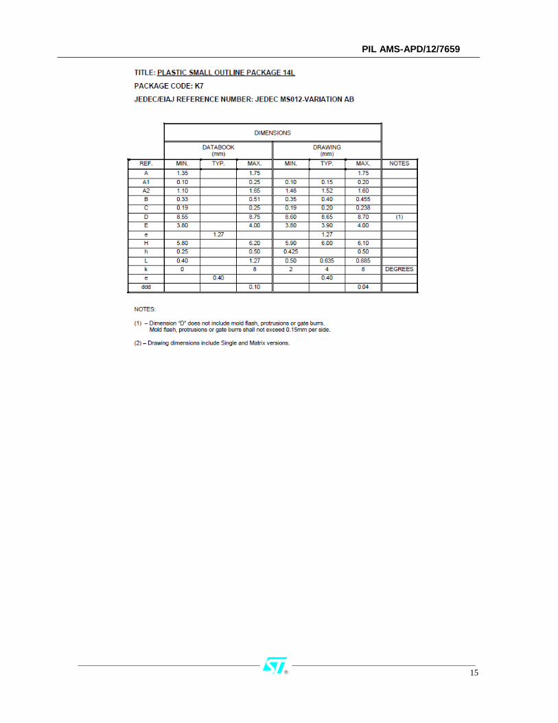
PIL AMS-APD/12/7659
15

PIL AMS-APD/12/7659
16
For DIP14 package:

PIL AMS-APD/12/7659
17
6.2 Tests Description
Test name Description Purpose Die Oriented
HTOL High Temperature
Operating Life
HTB High Temperature
Bias
The device is stressed in static or dynamic configuration, approaching the operative max. absolute ratings in terms of junction temperature and bias condition.
To determine the effects of bias conditions and temperature on solid state devices over time. It simulates the devices’ operating condition in an accelerated way. The typical failure modes are related to, silicon degradation, wire-bonds degradation, oxide faults.
HTSL High Temperature
Storage Life
The device is stored in unbiased condition at the max. temperature allowed by the pack-age materials, sometimes higher than the max. operative temperature.
To investigate the failure mechanisms activated by high temperature, typically wire-bonds sol-der joint ageing, data retention faults, metal stress-voiding.
ELFR Early Life Failure
Rate
The device is stressed in biased conditions at the max junction temperature.
To evaluate the defects inducing failure in ear-ly life.
Package Oriented
PC Preconditioning
The device is submitted to a typical temper-ature profile used for surface mounting de-vices, after a controlled moisture absorption.
As stand-alone test: to investigate the moisture sensitivity level. As preconditioning before other reliability tests: to verify that the surface mounting stress does not impact on the subsequent reliability performance. The typical failure modes are "pop corn" effect and delamination.
AC Auto Clave (Pres-
sure Pot)
The device is stored in saturated steam, at fixed and controlled conditions of pressure and temperature.
To investigate corrosion phenomena affecting die or package materials, related to chemical contamination and package hermeticity.
TC Temperature Cy-
cling
The device is submitted to cycled tempera-ture excursions, between a hot and a cold chamber in air atmosphere.
To investigate failure modes related to the thermo-mechanical stress induced by the dif-ferent thermal expansion of the materials inter-acting in the die-package system. Typical fail-ure modes are linked to metal displacement, dielectric cracking, molding compound delam-ination, wire-bonds failure, die-attach layer degradation.
THB Temperature Humi-
dity Bias
The device is biased in static configuration minimizing its internal power dissipation, and stored at controlled conditions of ambi-ent temperature and relative humidity.
To evaluate the package moisture resistance with electrical field applied, both electrolytic and galvanic corrosion are put in evidence.
Other
ESD Electro Static Dis-
charge
The device is submitted to a high voltage peak on all his pins simulating ESD stress according to different simulation models. CBM: Charged Device Model HBM: Human Body Model MM: Machine Model
To classify the device according to his suscep-tibility to damage or degradation by exposure to electrostatic discharge.
LU Latch-Up
The device is submitted to a direct current forced/sunk into the input/output pins. Re-moving the direct current no change in the supply current must be observed.
To verify the presence of bulk parasitic effect inducing latch-up.

PIL AMS-APD/12/7659
18
6.3 ESD certificates

PIL AMS-APD/12/7659
19

PIL AMS-APD/12/7659
20
6.4 LU certificates
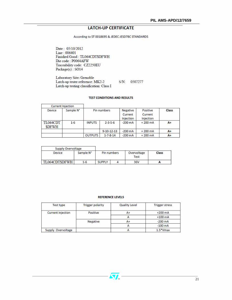
PIL AMS-APD/12/7659
21

PIL AMS-APD/12/7659 - Dated 27 Dec 2012
Please Read Carefully:
Information in this document is provided solely in connection with ST products. STMicroelectronics NV and its subsidiaries(‘‘ST’’) reserve theright to make changes, corrections, modifications or improvements, to this document, and the products and services described herein at anytime, without notice.
All ST products are sold pursuant to ST’s terms and conditions of sale.
Purchasers are solely responsible for the choice, selection and use of the ST products and services described herein, and ST assumes noliability whatsoever relating to the choice, selection or use of the ST products and services described herein.
No license, express or implied, by estoppel or otherwise, to any intellectual property rights is granted under this document. If any part of thisdocument refers to any third party products or services it shall not be deemed a license grant by ST for the use of such third party productsor services, or any intellectual property contained therein or considered as a warranty covering the use in any manner whatsoever of suchthird party products or services or any intellectual property contained therein.
UNLESS OTHERWISE SET FORTH IN ST’S TERMS AND CONDITIONS OF SALE ST DISCLAIMS ANY EXPRESS OR IMPLIEDWARRANTY WITH RESPECT TO THE USE AND / OR SALE OF ST PRODUCTS INCLUDING WITHOUT LIMITATION IMPLIEDWARRANTIES OF MERCHANTABILITY, FITNESS FOR A PARTICULAR PURPOSE ( AND THEIR EQUIVALENTS UNDER THE LAWSOF ANY JURISDICTION ), OR INFRINGEMENT OF ANY PATENT, COPYRIGHT OR OTHER INTELLECTUAL PROPERTY RIGHT.
UNLESS EXPRESSLY APPROVED IN WRITING BY TWO AUTHORIZED ST REPRESENTATIVES, ST PRODUCTS ARE NOTRECOMMENDED, AUTHORIZED OR WARRANTED FOR USE IN MILITARY, AIR CRAFT, SPACE, LIFE SAVING, OR LIFE SUSTAININGAPPLICATIONS, NOR IN PRODUCTS OR SYSTEMS WHERE FAILURE OR MALFUNCTION MAY RESULT IN PERSONAL INJURY,DEATH, OR SEVERE PROPERTY OR ENVIRONMENTAL DAMAGE. ST PRODUCTS WHICH ARE NOT SPECIFIED AS ‘‘AUTOMOTIVEGRADE’’ MAY ONLY BE USED IN AUTOMOTIVE APPLICATIONS AT USER’S OWN RISK.
Resale of ST products with provisions different from the statements and/or technical features set forth in this document shall immediately voidany warranty granted by ST for the ST product or service described herein and shall not create or extend in any manner whatsoever, anyliability of ST.
ST and the ST logo are trademarks or registered trademarks of ST in various countries.
Information in this document supersedes and replaces all information previously supplied.
The ST logo is a registered trademark of STMicroelectronics. All other names are the property of their respective owners
c 2012 STMicroelectronics - All rights reserved.
STMicroelectronics group of companies
Australia - Belgium - Brazil - Canada - China - Czech Republic - Finland - France - Germany - Hong Kong - India - Israel - Italy - Japan -
Malaysia - Malta - Morocco - Philippines - Singapore - Spain - Sweden - Switzerland - United Kingdom - United States of America
www.st.com
® 25/25