
Piezo Film Sensors Technical Manual
73
Images SI Inc. Sensor Products Division Staten Island NY 10312 Tel: 718.966.3694 FAX: &18.966.3695 Internet: www.imagesco.com e-mail: [email protected] Piezo Film Sensors Technical Manual
Transcript of Piezo Film Sensors Technical Manual

Images SI Inc. Sensor Products Division Staten Island NY 10312 Tel: 718.966.3694 FAX: &18.966.3695 Internet: www.imagesco.com e-mail: [email protected]
Piezo Film Sensors Technical Manual
ii
-- TABLE OF CONTENTS – Introduction .............................................................................................................1 Background ..............................................................................................................1 Piezoelectric Film Properties .................................................................................2 Table 1. Typical properties of piezo film...................................................3 Table 2. Comparison of piezoelectric materials........................................4 Operating Properties for a Typical Piezo Film Element ...................................4 Lead Attachment Techniques for Piezo Film Sensors.......................................8 Frequency Response .............................................................................................13 Piezo Film at Low Frequencies ...........................................................................14 Table 3. Capacitance values of common piezo film components .......15 Temperature Effects .............................................................................................25 Piezoelectric Cable and Properties......................................................................26 Table 4. Piezo Cable Typical Properties ..................................................26 Piezoelectric Basics................................................................................................27 Pyroelectric Basics .................................................................................................34 Table 5. Comparison of pyroelectric materials .......................................35 Basic Circuit Concepts..........................................................................................36 Manufacturing........................................................................................................43 Applications............................................................................................................43 Switches ........................................................................................................43 Beam Switch.................................................................................................44 Snap-Action Switches .................................................................................44 Impact Sensors ............................................................................................45 Impact Printers..................................................................................45 Sports Scoring....................................................................................45 Musical Instruments .........................................................................45 Traffic Sensors...................................................................................46 Vibration Sensing ........................................................................................47 Music Pickups....................................................................................47 Machine Monitoring .........................................................................48 Bearing Wear Sensors.......................................................................48 Fan Flow Sensor ...............................................................................48 Vending Sensors................................................................................48 Accelerometers ............................................................................................48 Table 6. Accelerometer Family .......................................................50 Table 7. Accelerometer Applications .............................................51 Ultrasound Applications ............................................................................52 Medical Imaging Ultrasound ...........................................................52 NonDestructive Testing (NDT) .....................................................53 Acoustic Emission ............................................................................53

iii
Fluid Level Sensor ............................................................................53 Air Ranging Ultrasound ...................................................................54 Audio.............................................................................................................55 Speakers..............................................................................................55 Microphones ......................................................................................55 Appendix A – Applications of Piezo Film ..............................................56


Page 1
INTRODUCTION Transducer materials convert one form of energy into another, and are widely used in sensing applications. The tremendous growth in the use of microprocessors has propelled the demand for sensors in diverse applications. Today, PIEZOELECTRIC POLYMER SENSORS are among the fastest growing of the technologies within the $18 billion worldwide sensor market. Like any new technology, there have been an extraordinary number of applications where "PIEZO FILM" has been considered for the sensor solution. In the 20 years since the discovery of piezoelectric polymer, the technology has matured, practical applications have emerged from a long list of possibilities, and the rate of commercialization of the technology is accelerating. These documents provide an overview of piezoelectric polymer technology and nomenclature, its properties, and sensor design considerations. It also explores a range of sensor applications that have been successfully developed in recent years. Solving unique sensor problems is a particular strength of our group of applications engineers. We welcome the opportunity to provide assistance to you during your evaluation of piezo film sensors for your design. BACKGROUND Piezoelectricity, Greek for "pressure" electricity, was discovered by the Curie brothers more than 100 years ago. They found that quartz changed its dimensions when subjected to an electrical field, and conversely, generated electrical charge when mechanically deformed. One of the first practical applications of the technology was made in the 1920's by another Frenchman, Langevin, who developed a quartz transmitter and receiver for underwater sound - the first SONAR. Before World War II, researchers discovered that certain ceramic materials could be made piezoelectric when subjected to a high polarizing voltage, a process analogous to magnetizing a ferrous material. By the 1960's, researchers had discovered a weak piezoelectric effect in whale bone and tendon. This began an intense search for other organic materials that might exhibit piezoelectricity. In 1969, Kawai found very high piezo-activity in the polarized fluoropolymer, polyvinylidene fluoride (PVDF). While other materials, like nylon and PVC exhibit the effect, none are as highly piezoelectric as PVDF and its copolymers. Like some other ferroelectric materials, PVDF is also pyroelectric, producing electrical charge in response to a change in temperature. PVDF strongly absorbs infrared energy in the 7-20:m wavelengths (see Figure 1), covering the same wavelength spectrum as heat from the human body. Accordingly, PVDF makes a useful human motion sensor as well as pyroelectric sensor for more sophisticated applications like vidicon cameras for night
Figure 1. Typical infrared absorption spectrum of PVDF film.

Page 2
vision and laser beam profiling sensors. A dense infrared array has been recently introduced that identifies one’s fingerprint pattern using the pyro effect of piezo polymer. New copolymers of PVDF, developed over the last few years, have expanded the applications of piezoelectric polymer sensors. These copolymers permit use at higher temperatures (135EC) and offer desirable new sensor shapes, like cylinders and hemispheres. Thickness extremes are possible with copolymer that cannot be readily attained with PVDF. These include ultrathin (200 Å) spin-cast coatings that enable new sensor-on-silicon applications, and cylinders with wall thicknesses in excess of 1200:m for sonar. Piezo cable is also produced using copolymer. PIEZOELECTRIC FILM PROPERTIES Piezo film is a flexible, lightweight, tough engineering plastic available in a wide variety of thicknesses and large areas. Its properties as a transducer include: • Wide frequency range—0.001 Hz to 109 Hz. • Vast dynamic range (10-8 to 106 psi or : torr to Mbar). • Low acoustic impedance—close match to water, human tissue and adhesive systems. • High elastic compliance • High voltage output—10 times higher than piezo ceramics for the same force input. • High dielectric strength—withstanding strong fields (75V/:m) where most piezo ceramics
depolarize. • High mechanical strength and impact resistance (109—1010 Pascal modulus). • High stability—resisting moisture (<0.02% moisture absorption), most chemicals, oxidants, and
intense ultraviolet and nuclear radiation. • Can be fabricated into unusual designs. • Can be glued with commercial adhesives. One major advantage of piezo film over piezo ceramic is its low acoustic impedance which is closer to that of water, human tissue and other organic materials. For example, the acoustic impedance (ZO = D L) of piezo film is only 2.6 times that of water, whereas piezo ceramics are typically 11 times greater. A close impedance match permits more efficient transduction of acoustic signals in water and tissue. Piezo film does have some limitations for certain applications. It makes a relatively weak electromechanical transmitter when compared to ceramics, particularly at resonance and in low frequency applications. The copolymer film has maximum operating/storage temperatures as high as 135oC, while PVDF is not recommended for use or storage above 100 EC. Also, if the electrodes on the film are exposed, the sensor can be sensitive to electromagnetic radiation. Good shielding techniques are available for high EMI/RFI environments. Table 1 lists typical properties of piezo film. Table 2 provides a comparison of the piezoelectric properties of PVDF polymer and two popular piezoelectric ceramic materials. Piezo film has low density and excellent sensitivity, and is mechanically tough. The compliance of piezo film is 10 times greater than the compliance of ceramics. When extruded into thin film, piezoelectric polymers can be directly attached to a structure without disturbing its mechanical motion. Piezo film is well suited to strain sensing applications requiring very wide bandwidth and high sensitivity. As an actuator, the polymer's low acoustic impedance permits the efficient transfer of a broadband of energy into air and other gases.

Page 3
Table 1. Typical properties of piezo film
Symbol Parameter PVDF Copolymer Units t Thickness 9, 28, 52, 110 <1 to 1200 :m (micron, 10-6 )
d31 23 11
d33
Piezo Strain Constant
-33 -38
func {{m/m} over {V/m}}~\or~{func {C/m SUP 2} over {N/m SUP
g31 216 162
g33
Piezo Stress constant
-330 -542
{func{V/m} over {N/m SUP 2}}~func \or~{func{m/m} over
k31 12% 20%kt
Electromechanical Coupling Factor 14% 25-29%
C Capacitance 380 for 28:m 68 for 100:m pF/cm2, @ 1KHz
Y Young’s Modulus 2-4 3-5 109 N/m2 1.5 2.3 V0 Speed of
Sound stretch:
thickness: 2.2 2.4 103 m/s
p Pyroelectric Coefficient 30 40 10-6 C/m2 EK
, Permittivity 106-113 65-75 10-12 F/m
,/, 0 Relative Permittivity 12-13 7-8
func { Mass Density 1.78 1.82 103kg/m
rho Volume Resistivity >1013 >1014 Ohm meters
R SUB <3.0 <3.0 Ohms/square for NiAl
R SUB Surface Metallization
Resistivity 0.1 0.1 Ohms/square for Ag Ink
tan *e Loss Tangent 0.02 0.015 @ 1KHz
Yield Strength 45-55 20-30 106 N/m2 (stretch axis)
Temperature Range -40 to 80...100 -40 to 115...145 func{DEG C} Water Absorption <0.02 <0.02 % H2O
Maximum Operating Voltage 750 (30) 750 (30) V/mil(V/:m), DC, @ 25EC
Breakdown Voltage 2000 (80) 2000 (80) V/mil(V/:m), DC, @ 25EC

Page 4
Table 2. Comparison of piezoelectric materials
Property Units PVDF Film PZT BaTi03 Density 103kg/m3 1.78 7.5 5.7 Relative Permittivity ,/, 0 12 1,200 1,700 d31 Constant (10-12)C/N 23 110 78 g31 Constant (10-3)Vm/N 216 10 5 k31 Constant % at 1 KHz 12 30 21 Acoustic Impedance (106)kg/m2-sec. 2.7 30 30
OPERATING PROPERTIES FOR A TYPICAL PIEZO FILM ELEMENT The DT1 element is a standard piezo film configuration consisting of a 12x30 mm active area printed with silver ink electrodes on both surfaces of a 15x40 mm die-cut piezo polymer substrate. 1. Electro-Mechanical Conversion (1 direction) 23 x 10-12m/V, 700 x 10-6N/V (3 direction) -33 x 10-12m/V 2. Mechano-Electrical Conversion (1 direction) 12 x 10-3V per microstrain, 400 x 10-3V/:m, 14.4V/N (3 direction) 13 x 10-3V/N 3. Pyro-Electrical Conversion 8V/ o K (@ 25 o C) 4. Capacitance
1.36 x 10⁻⁹F; Dissipation Factor of 0.018 @ 10 KHz; Impedance of 12 KS @ 10 KHz 5. Maximum Operating Voltage DC: 280 V (yields 7 :m displacement in 1 direction) AC: 840 V (yields 21 :m displacement in 1 direction) 6. Maximum Applied Force (at break, 1 direction)
6-9 kgF (yields voltage output of 830 to 1275 V) Electrical to Mechanical Conversion Large displacements of forces are not generally available from piezo film. This becomes apparent when designing loudspeaker elements for instance, as low frequency performance (below 500Hz) tends to be limited. Even a large sheet of film is unable to create high amplitude pressure pulses as low audio frequencies. This does not apply, however, to low to high frequency ultrasonic frequencies, as seen in current designs for ultrasound air ranging transducers (40-50 KHz) and in medical ultrasonic imaging applications. In enclosed air cavities (headset speakers, hearing aids), the low frequency response of piezo film is excellent. For air ranging ultrasound, the piezo film element height controls vertical beam angle and the curvature and width of the transducer controls

Page 5
horizontal beam pattern. Piezo film air ranging transducers can provide up to 360 o field of view, ranging object from a few centimeters to several meters with high resolution. Bimorph configurations (like a bimetal strip) allow the small differential displacement of two reverse-connected elements to be translated into substantial flexural motion. Small fans or optical deflectors can thus be created. Such devices consume very little real power (being capacitive in nature). Large devices may be difficult to drive due to high capacitance, especially when transformers are used to step up the drive voltage. Good amplifier design is important. Nevertheless, conventional fan and blower technologies generate higher flow rates and back pressures than piezo bimorphs. Although the forces involved are small, the film can be used to excite other mechanical structures over a very wide frequency range. If a second element of film is used to receive the induced vibration, the system can possess a very high dynamic range, even though the overall "insertion loss" due to the film is about -66 dB typically for a structure at resonance. If sufficient gain is applied between these elements, the structure will self-oscillate at its natural frequency. For these resonant mechanical systems, high voltage drive is not required. The amplifier circuit may function adequately from a normal dual rail op-amp supply, or even from a single 9 volt battery. For analysis purposes, even lower applied voltages, e.g., the noise source of a spectrum analyzer at 70 mVrms, are sufficient to insert the mechanical energy into a structure when piezo film is also used to monitor the result. Mechanical to Electrical Conversion The sensitivity of piezo film as a receiver of mechanical work input is awesome. In its simplest mode the film behaves like a dynamic strain gage except that it requires no external power source and generates signals greater than those from conventional foil strain gages after amplification. Frequency response is thus free from any limitations imposed by the need for high gains and will extend up to the wavelength limit of the given transducer. The extreme sensitivity is largely due to the format of the piezo film material. The low thickness of the film makes, in turn, a very small cross-sectional area and thus relatively small longitudinal forces create very large stresses within the material. It is easy to exploit this aspect to enhance the sensitivity parallel to the machine axis. If a laminated element of film (for example an LDT1-028K) is placed between two layers of compliant material then any compressive forces are converted into much larger longitudinal extensive forces. In fact, this effect tends to predominate in most circumstances since most substances are compliant to some extent and the ratio of effective sensitivity in the 1 (length) vs 3 (thickness) directions is typically 1000:1. Piezo film transducers may often cover a much larger area than normal strain gages so any direct comparisons should be performed in a uniform strain field for meaningful results. Obviously "point"-type transducers could be used where required although the capacitance of a very small area will require consideration. The low frequency limit of operation will be defined by the greatest resistive load achievable, or by the largest capacitance load that still allows the signal to be easily detected. Operation down to fractions of Hz can be achieved using either conventional charge amplifiers or, since signal levels are relatively high, simple high impedance FET buffer circuits.
1. DT1 Element in [mm]
Page 6
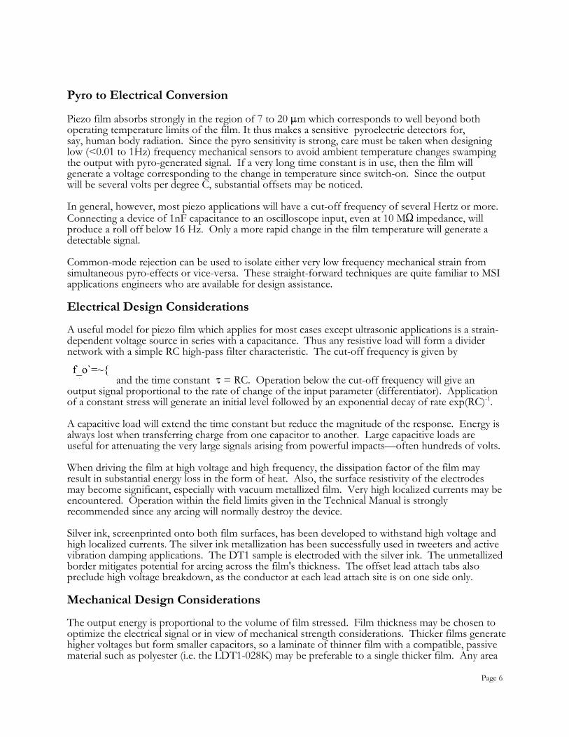
Pyro to Electrical Conversion Piezo film absorbs strongly in the region of 7 to 20 :m which corresponds to well beyond both operating temperature limits of the film. It thus makes a sensitive pyroelectric detectors for, say, human body radiation. Since the pyro sensitivity is strong, care must be taken when designing low (<0.01 to 1Hz) frequency mechanical sensors to avoid ambient temperature changes swamping the output with pyro-generated signal. If a very long time constant is in use, then the film will generate a voltage corresponding to the change in temperature since switch-on. Since the output will be several volts per degree C, substantial offsets may be noticed. In general, however, most piezo applications will have a cut-off frequency of several Hertz or more. Connecting a device of 1nF capacitance to an oscilloscope input, even at 10 MS impedance, will produce a roll off below 16 Hz. Only a more rapid change in the film temperature will generate a detectable signal. Common-mode rejection can be used to isolate either very low frequency mechanical strain from simultaneous pyro-effects or vice-versa. These straight-forward techniques are quite familiar to MSI applications engineers who are available for design assistance. Electrical Design Considerations A useful model for piezo film which applies for most cases except ultrasonic applications is a strain-dependent voltage source in series with a capacitance. Thus any resistive load will form a divider network with a simple RC high-pass filter characteristic. The cut-off frequency is given by
and the time constant J = RC. Operation below the cut-off frequency will give an output signal proportional to the rate of change of the input parameter (differentiator). Application of a constant stress will generate an initial level followed by an exponential decay of rate exp(RC)-1. A capacitive load will extend the time constant but reduce the magnitude of the response. Energy is always lost when transferring charge from one capacitor to another. Large capacitive loads are useful for attenuating the very large signals arising from powerful impacts—often hundreds of volts. When driving the film at high voltage and high frequency, the dissipation factor of the film may result in substantial energy loss in the form of heat. Also, the surface resistivity of the electrodes may become significant, especially with vacuum metallized film. Very high localized currents may be encountered. Operation within the field limits given in the Technical Manual is strongly recommended since any arcing will normally destroy the device. Silver ink, screenprinted onto both film surfaces, has been developed to withstand high voltage and high localized currents. The silver ink metallization has been successfully used in tweeters and active vibration damping applications. The DT1 sample is electroded with the silver ink. The unmetallized border mitigates potential for arcing across the film's thickness. The offset lead attach tabs also preclude high voltage breakdown, as the conductor at each lead attach site is on one side only. Mechanical Design Considerations The output energy is proportional to the volume of film stressed. Film thickness may be chosen to optimize the electrical signal or in view of mechanical strength considerations. Thicker films generate higher voltages but form smaller capacitors, so a laminate of thinner film with a compatible, passive material such as polyester (i.e. the LDT1-028K) may be preferable to a single thicker film. Any area
f_o`=~{1}

Page 7
of film that is not undergoing stress will act as a capacitive load on the "active" area and should be minimized if required. Most metallizations are subject to corrosion, especially when handled. Thin conformal coatings or laminates are frequently applied to maintain surface quality. Acrylics adhesives, synthetic rubber resins, epoxies and cyano-acrylates are all frequently employed in lamination and assembly. Some designs may use external metallic or conductive substrates as the electrodes, in which case unmetallized film may be used to good advantage. The external metal surface can be in direct contact with the unmetallized film to collect the charge, or, capacitive coupling through thin adhesive tapes or epoxy layers can be employed for ac applications. Patterning of the electrodes is especially useful for defining specific active areas on a continuous sheet and also to allow die-cutting of elements with a clear border around the cut area. Displacement (offset) of upper and lower electrode tabs at the connection point is good practice to prevent unpredictable piezo behavior in this area caused by the influence of the wire terminations. This also allows low cost penetrative lead-attach methods to be used (crimps or eyelets). Joint Electrical and Mechanical Design Considerations The capacitive nature of piezo film devices implies that they are susceptible to Electro Magnetic Interference (EMI). This becomes increasingly more important as the output signal level drops. EMI can be ignored where the output is high or when the film is being driven in a non-critical environment. A.C. mains interference may become a problem with unshielded devices. Another potential problem exists when one electrode element is being driven and an another is receiving the vibration signal. Care must be taken to avoid "crosstalk". Use of ready-made shielded elements (SDT1-028K) supplied with coaxial cable eliminates these problems, but simple measures may be taken with any device to avoid interference. Unwanted frequencies may be filtered out electronically. If the sensor is to be mounted on a conductive substrate, then this may form one half of a grounded envelope, with the outer electrode forming the other half. Lightweight shielded cable is readily available and is an alternative to twisted pair wires. Attention should be paid to the point of connection itself as this is also an area of EMI vulnerability. Durable lead attachment techniques have been fully developed by MSI, and most products are supplied with leads preattached. As indicated, some form of coaxial cable is often employed and must be interfaced to a very thin flexible material. Reinforcement at the lead attach site may be required, which can introduce some acoustic effects into the transducer if the interconnection site is free to vibrate. Thin copper foil backed with a conductive adhesive can provide excellent but non-permanent connections to the film. An area of 1 cm² will give a contact resistance of a few mS s. Crimp-through connectors as used for flexible circuits are routinely used with offset electrode patterns, but thin films require some physical reinforcement for good results. Polyester reinforcement at the lead attach site is a common method to ruggedize the interconnection. The stiffener may lie between the crimp and the electrode with only minor degradation of contact resistance. Typical values are 150-500 mS. Miniature rivets, eyelets and even nuts and bolts, with washers, all combine great strength with good contact resistance at typically less than 100 mS. These techniques may be used to connect to cables using solder tags, or direct onto printed circuit boards.

Page 8
Clamping methods, either direct to the conductive traces on the PCB or using conductive rubber, ZEBRA® connectors, lugs and washers have all been used with success. Direct connection using silver-loaded (conductive) epoxy also works well, but requires curing time, often at elevated temperature, for best results. As indicated earlier, other materials may form the electrodes themselves, such as PCB traces or conductive rubber. Capacitive coupling through thin adhesive layers is practical under some a.c. circumstances, allowing some unusual transducer designs with apparently no lead attachment at all! ZEBRA is a registered trademark of Fujipoly.
ACTIVE PIEZO FILM AREA(TOP & BOTTOM ELECTRODES OVERLAP)
TOP ELECTRODEACTIVE PIEZO FILM AREA
TOP ELECTRODE
BOTTOM ELECTRODE
BOTTOM ELECTRODE
A A
CROSS SECTION A-A
AA
CROSS SECTION A-A
B
BCROSS SECTION B-B
DT PATTERN
KEYHOLE PATTERN

Page 9
LEAD ATTACHMENT TECHNIQUES FOR PIEZO FILM SENSORS Introduction How to make reliable interconnection to piezo film is one of the most frequently asked customer questions. With this in mind, MSI has paid great attention to the development of techniques to simplify interconnection to piezo film elements. Today, most of the sensor elements supplied to customers from our Division have leads already attached. The aim of this article is to examine and discuss available interconnection options. Some of the most convenient interconnection techniques require that MSI apply patterned electrodes on one or both surfaces of the piezo film—this can always be done to customers' requirements during manufacture— alternatively, a simple method achieving the same goal is presented at the end of the text. In general, patterned electrodes are achieved during piezo film manufacturing by screen printing conductive inks, metal masking during sputtered electrode deposition, or chemically etching patterns by photolithographic techniques. The Targets Considered here are the design objectives desired for the lead-attach method. Not all objectives can be achieved with any one technique. Designers should identify the most important objectives and select among the interconnection options accordingly. ! High conductivity/low resistance — surprisingly, high conductivity interconnection is not a
particularly important parameter for most piezoelectric applications. Piezo transducers are frequently used in high-impedance circuits where inclusion of a few ohms does not usually affect performance. More important, however, is consistence—the resistance should not fluctuate during use since this will introduce a source of electrical noise.
! Low mass — this is especially important when the piezo film is not to be clamped to a mechanical support structure. The acoustic effect created by the mechanical vibration of the mass of the interconnection on an otherwise flexible structure can be dramatic.
! Low profile — many piezo film applications arise by virtue of the low thicknesses of piezo film. Interrupting this with bulk terminations is often prohibited. Contact vibration sensors can show distinct resonances if film is not bonded flush to the contact surface to include the interconnection.
! Flexibility — here again is a property that must often match that of the film itself. Some degree of flexibility is a distinct advantage in many applications.
! Low area — useful piezo devices can be quite literally be employed as "point" receivers. Small piezo-active areas (where the top and bottom conductors fully overlap) can be configured with displaced or off-set lead-attach tabs. The top and bottom tabs are off-set with respect to each other (when viewed through the film thickness). This allows a precisely defined active area
Figure 4. Typical piezo film patterns
PIEZO FILM
P.C.B.
P.C.B. TRACE
TOP ELECTRODE
WASHER
BOLT
BOTTOM ELECTRODE
P.C.B.
PLATED THROUGH HOLE
TOP ELECTRODE
P.C.B. TRACE
DT PATTERN BOLTED TO P.C.B

Page 10
(overlapped electrodes) with non-piezo conductors (off-set tabs) leading to remote bonding sites, a technique most frequently employed for "small" devices.
! Mechanical Strength — very often the greatest strain experienced by a polymer transducer is around the connection, whether by accident (tripping over the cable) or by design. In general, those methods which involve the interconnection penetrating through the film at the off-set tab locations with crimps, eyelets or rivets yield the best ultimate strain resistance. Often the lead attach area is reinforced with polyester to improve the strength of the penetrative interconnection.
! Long-term Stability — including all the usual environmental parameters. Most interconnections have unlimited life (crimps, eyelets, conductive rubber connectors). Others have a more limited shelf life (conductive tapes)
! Speed and Ease of application — of particular importance when high volume production is planned. Many interconnection techniques are supported by semi-automatic equipment for volume production (crimps, eyelets) while others are labor intensive (conductive adhesives).
! Electrical strength — an issue associated mainly with electrically driven (high voltage) elements such as loudspeakers and actuators.
The Design Considerations Two major issues control the selection of lead-attach methods: ! Is anchorage of the film allowed at the site of lead-attach? This can be a major advantage, for
example, direct connection or capacitive coupling to the conductive traces of a printed-circuit board.
! Is special patterning of the film available, which would allow penetrative techniques? (with MSI Sensors custom patterning service, the answer is almost always "yes.") Simple experimental methods allow the same result.
This concludes the "questions" section—now, hopefully, are the "answers." The Methods Penetrative - Here the techniques involve piercing the film (and possibly additional reinforcing laminates to give sufficient thickness and strength), and thus the film should be patterned with a displaced or off-set lead-out arrangement to prevent shorting of upper and lower electrodes by the inserted connector. ! Rivets or eyelets can be
affixed to the off-set conductive traces on the piezo film. Included between the eyelet or rivet can be a ring tongue lug terminal with wire attached. The eyelet or rivet mechanically presses the conductive ring against the off-set patterned electrode to make reliable interconnection.
!
Figure 4.
Figure 6.

Page 11
To affix the piezo film directly to a PCB, small "POP" or "blind" rivets or eyelets can be used in conjunction with patterned film electrodes and the conductive tracks on the PCB to allow a single operation to form the interconnection. During screen printing of conductive ink electrodes, a small “plated through hole” can be formed in one of the off-set tabs, thereby bringing both conductors to the same side of the piezo film. This greatly facilitates riveting the film electrode tabs to the corresponding PCB traces. If the “plated through hole” technique is not used, then the top film electrode can be electrically connected by the rivet to a conductive trace on the underside of the PCB. The bottom film electrode is electrically connected to a corresponding trace on the top of the PCB and held in intimate contact by the pressure exerted by the rivet. ! Nuts and bolts - Wires terminated with washers, ring-tongue lugs, solder-tags, etc. can easily
be incorporated with small nuts and bolts. ! Crimp Connectors — generally, crimps designed for flexible circuit technology work well
with piezo film elements. Crimps can have solder tabs for affixing wires, or the crimp ends can be inserted into corresponding holes in a PCB and soldered to the underside of the PCB (maximum of a few second soldering time so as not to overheat the film). Like the eyelets mentioned above, crimps are normally designed to work with a specified thickness of "substrate," so film may require "padding" on one side (i.e., polyester reinforcement) to accommodate the crimp connectors. Additionally, a complete multi-way connector may be crimped to a more complex device, giving straight plug-in compatibility with other connectors.
Figure 5.
TOP ELECTRODE
BOTTOM ELECTRODE
A A
CROSS SECTION A-A
PLATED THROUGH HOLE
P.C.B
TRACE ON P.C.B
A
A
PIEZO FILMOR FLEX CIRCUIT
PLATED THROUGH HOLE
Page 12
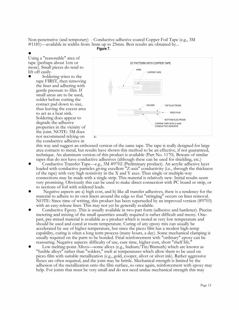
Non-penetrative (and temporary) - Conductive-adhesive coated Copper Foil Tape (e.g., 3M #1181)—available in widths from 3mm up to 25mm. Best results are obtained by... ! Using a "reasonable" area of tape (perhaps about 1cm or more). Small pieces do tend to lift off easily. ! Soldering wires to the
tape FIRST, then removing the liner and adhering with gentle pressure to film. If small areas are to be used, solder before cutting the contact pad down to size, thus leaving the excess area to act as a heat sink. Soldering does appear to degrade the adhesive properties in the vicinity of the joint. NOTE: 3M does not recommend relying on the conductive adhesive in this way and suggest an embossed version of the same tape. The tape is really designed for large area contacts to metal, but results have shown this method to be an effective, if not guaranteed, technique. An aluminum version of this product is available (Part No. 1170). Beware of similar tapes that do not have conductive adhesives (although these can be used for shielding, etc.)
! Conductive Transfer Tape—e.g., 3M #9702 (Preliminary product). An acrylic adhesive layer loaded with conductive particles giving excellent "Z-axis" conductivity (i.e., through the thickness of the tape) with very high resistivity in the X and Y axes. Thus single or multiple-way connections may be made with a single strip. This material is relatively new. Initial results seem very promising. Obviously this can be used to make direct connection with PC board or strip, or to sections of foil with soldered leads.
! Negative aspects are a) high cost, and b) like all transfer adhesives, there is a tendency for the material to adhere to its own liners around the edge so that "stringing" occurs on liner removal. NOTE: Since time of writing, this product has been superseded by an improved version (#9703) with an easy-release liner. This may not yet be generally available.
! Conductive Epoxy. This is usually available in two-part form (adhesive and hardener). Precise metering and mixing of the small quantities usually required is rather difficult and messy. One-part, pre-mixed material is available as a product which is stored at very low temperature and should be used and cured at room temperature. Curing of any epoxy mix can usually be accelerated by use of higher temperature, but since the piezo film has a modest high-temp capability, curing is often a long term process (many hours, a day). Some mechanical clamping is usually required on the parts to be bonded. Final reinforcement with "ordinary" epoxy can be reassuring. Negative aspects: difficulty of use, cure time, higher cost, short "shelf life."
! Low melting-point Alloys—some alloys (e.g., Indium/Tin/Bismuth) which are known as "fusible alloys" rather than "solders," melt at temperatures which allow them to be used on piezo film with suitable metallization (e.g., gold, cooper, silver or silver ink). Rather aggressive fluxes are often required, and the joint may be brittle. Mechanical strength is limited by the adhesion of the metallization onto the film surface, so once again, reinforcement with epoxy may help. For joints that must be very small and do not need undue mechanical strength this may
Figure 7.
2.
COPPER TAPE
PIEZO FILM
SOLDER
WIRE
TOP ELECTRODE
BOTTOM ELECTRODE
COPPER TAPE WITH Z-AXISCONDUCTIVE ADHESIVE
DT PATTERN WITH COPPER TAPE
Page 13
prove a valuable technique. Negative aspects: only certain metallizations are appropriate, sample quantities hard to come by. Mechanical strength limited [Indium Corp.]
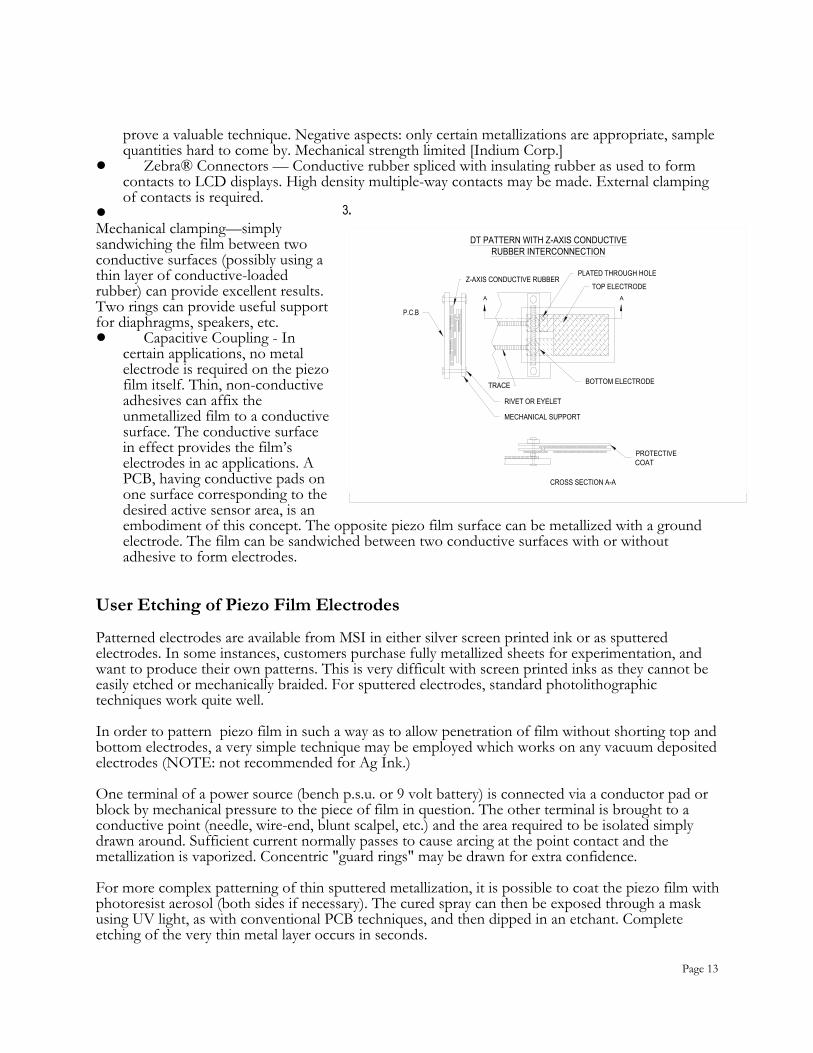
! Zebra® Connectors — Conductive rubber spliced with insulating rubber as used to form contacts to LCD displays. High density multiple-way contacts may be made. External clamping of contacts is required.
! Mechanical clamping—simply sandwiching the film between two conductive surfaces (possibly using a thin layer of conductive-loaded rubber) can provide excellent results. Two rings can provide useful support for diaphragms, speakers, etc. ! Capacitive Coupling - In
certain applications, no metal electrode is required on the piezo film itself. Thin, non-conductive adhesives can affix the unmetallized film to a conductive surface. The conductive surface in effect provides the film’s electrodes in ac applications. A PCB, having conductive pads on one surface corresponding to the desired active sensor area, is an embodiment of this concept. The opposite piezo film surface can be metallized with a ground electrode. The film can be sandwiched between two conductive surfaces with or without adhesive to form electrodes.
User Etching of Piezo Film Electrodes Patterned electrodes are available from MSI in either silver screen printed ink or as sputtered electrodes. In some instances, customers purchase fully metallized sheets for experimentation, and want to produce their own patterns. This is very difficult with screen printed inks as they cannot be easily etched or mechanically braided. For sputtered electrodes, standard photolithographic techniques work quite well. In order to pattern piezo film in such a way as to allow penetration of film without shorting top and bottom electrodes, a very simple technique may be employed which works on any vacuum deposited electrodes (NOTE: not recommended for Ag Ink.) One terminal of a power source (bench p.s.u. or 9 volt battery) is connected via a conductor pad or block by mechanical pressure to the piece of film in question. The other terminal is brought to a conductive point (needle, wire-end, blunt scalpel, etc.) and the area required to be isolated simply drawn around. Sufficient current normally passes to cause arcing at the point contact and the metallization is vaporized. Concentric "guard rings" may be drawn for extra confidence. For more complex patterning of thin sputtered metallization, it is possible to coat the piezo film with photoresist aerosol (both sides if necessary). The cured spray can then be exposed through a mask using UV light, as with conventional PCB techniques, and then dipped in an etchant. Complete etching of the very thin metal layer occurs in seconds.
3.
TOP ELECTRODE
BOTTOM ELECTRODE
A A
CROSS SECTION A-A
PLATED THROUGH HOLE
P.C.B
TRACE
PROTECTIVECOAT
RIVET OR EYELET
MECHANICAL SUPPORT
Z-AXIS CONDUCTIVE RUBBER
DT PATTERN WITH Z-AXIS CONDUCTIVERUBBER INTERCONNECTION

Page 14
Copper/Nickel metallizations etch very well with standard PCB etchant (ferric chloride). Other metals require special etchants for good results (Aquaregia for gold). Remember that the metallization layer may only be a few hundred atoms thick (300-700 Å), and therefore fine traces are very vulnerable to scratching or cracking.

Page 15
High Voltage Techniques The use of piezo film as a vibration exciter requires separate consideration. Since the impedance of a capacitive transducer decreases with frequency and approaches infinity for low frequencies, very high voltages (a few hundred volts typically) may be required to drive, for example, full audio-range loudspeakers. Frequently, transformers are used to step up moderate voltages to supply the required drive signal. Under these circumstances, extreme stresses may be placed upon the connections. Consider first applying a voltage step of 30V to a capacitor of 100nF with an overall circuit resistance of 2 ohms. The initial current pulse peaks at 15 amps (assuming the supply is capable of supplying this). Such a current "spike" may well show up defects in connectors. Consider next a transformer which steps 12V signals up to 240V. A DC current in the primary of 200 :A (corresponding to an applied voltage of 0.5 volts), when broken, may cause a voltage surge of 830 volts across the secondary circuit, well in the excess of the expected X 20 magnification factor. Even with heavy capacitive loading, high voltages may be seen. Worse still, if the secondary circuit is broken, current pulses exceeding 60A with durations of only tens of nanoseconds may arise. Such phenomena should not trouble well-formed connections. But if a lead-attach method has been used which has any trapped air, the effect of the reduced dielectric constant may be to promote breakdown. Such events may be catastrophic, as the familiar crackling sound and lively blue sparks will testify. Solutions are: 1. Silver ink electrodes are a must - the thin sputtered electrodes cannot withstand the high voltages 2. Large area contacts to reduce stress. We paint silver ink around eyelets/rivets to provide extra conduction paths to the film electrode. 3. (Possibly) a semi-resistive contact pad to reduce current surges—equivalent to including a series resistance in the circuit. Practical values up to about 1 k will produce only a fractional loss in output and will reduce the magnitude of current spikes. FREQUENCY RESPONSE Unlike piezo ceramic transducers, piezo film transducers offer wide dynamic range and are also broadband. These wide band characteristics (near dc to 2GHz) and low Q are partly attributable to the polymers' softness. As audio transmitters, a curved piezo film element, clamped at each end, vibrates in the length (d31) mode, as shown in Figure 10. Piezo film is a very high fidelity tweeter, also used in novelty speakers for toys, inflatables and apparel. The d31 configuration (Figure 10) is also used for air ultrasound ranging applications up to frequencies of about 50 KHz. When used as a high ultrasonic transmitter (generally >500KHz), piezo film is normally operated in the thickness (d33) mode. Maximum transmission occurs at thickness resonance. The basic half-
wavelength resonance of 28:m piezo film is about 40 MHz:
Figure 10. Clamped film in d31 mode produces sound
f_r~=~{v} over {2t}~=~{2.2`x`10^3`m/sec} over {2`x`28`x`10^{-6}m}

Page 16
Resonance values thus depend on film thickness. They range from low MHz for thick films (1,000 ) to >100MHz for very thin films. Figure 11 shows the effect that frequency has on permittivity and dissipation factor at room temperature. As a result of its very low permittivity g (1 percent that of piezo ceramics), the film exhibits g-constants (voltage output coefficients) that are significantly greater than piezo ceramics (g = d/g). PIEZO FILM AT LOW FREQUENCIES Introduction The behavior of a piezo film component at low frequencies is fairly straightforward to describe in electrical terms, yet is quite frequently misunderstood. Since any practical application of the technology will most likely involve some consideration of this topic, it is the intent of this article to examine the subject at some length. The treatment is made as non-mathematical as possible, with verbal descriptions and real-world examples being used to illustrate the concepts. Some familiarity with the use of FFT techniques to transform between time-domain and frequency-domain descriptions is assumed, but not essential. Connecting Up In most instances, the first evaluation of piezo film begins with connecting a piezo component to an oscilloscope via a probe ("scope probe"). Under normal electronics circumstances, a scope probe can be considered to be an "infinite impedance" - so high, that its effect on the circuit under test can be neglected. Not so with piezo film - in many cases, a scope probe can act almost like a short-circuit. Typical probes, when plugged in to an oscilloscope, have an effective resistance of 1MS (one million ohms). Others may be fixed at 10MS, while many are conveniently switchable between "x1" ( 1MS) and "x10" (10MS). Note that the physical element comprising the 1MS resistance is usually built into the oscilloscope input stage, rather than being a discrete component within the probe itself. A "x1" probe is thus basically a length of shielded cable with suitable contacts attached to each end.
Figure 11. Dielectric permittivity and dissipation factor vs. frequency
�
/ �o tan e
Frequency (Hz)
Page 17
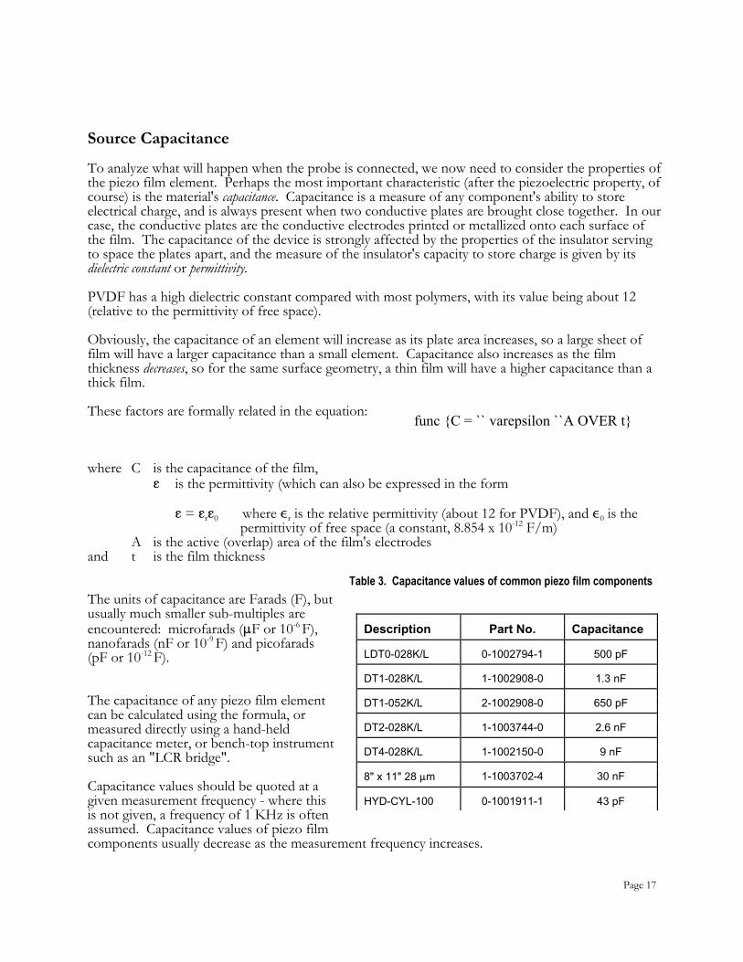
Source Capacitance To analyze what will happen when the probe is connected, we now need to consider the properties of the piezo film element. Perhaps the most important characteristic (after the piezoelectric property, of course) is the material's capacitance. Capacitance is a measure of any component's ability to store electrical charge, and is always present when two conductive plates are brought close together. In our case, the conductive plates are the conductive electrodes printed or metallized onto each surface of the film. The capacitance of the device is strongly affected by the properties of the insulator serving to space the plates apart, and the measure of the insulator's capacity to store charge is given by its dielectric constant or permittivity. PVDF has a high dielectric constant compared with most polymers, with its value being about 12 (relative to the permittivity of free space). Obviously, the capacitance of an element will increase as its plate area increases, so a large sheet of film will have a larger capacitance than a small element. Capacitance also increases as the film thickness decreases, so for the same surface geometry, a thin film will have a higher capacitance than a thick film. These factors are formally related in the equation: where C is the capacitance of the film,
g is the permittivity (which can also be expressed in the form
g = grg0 where ,r is the relative permittivity (about 12 for PVDF), and ,0 is the permittivity of free space (a constant, 8.854 x 10⁻¹² F/m)
A is the active (overlap) area of the film's electrodes and t is the film thickness The units of capacitance are Farads (F), but usually much smaller sub-multiples are encountered: microfarads (:F or 10-6 F), nanofarads (nF or 10-9 F) and picofarads (pF or 10-12 F). The capacitance of any piezo film element can be calculated using the formula, or measured directly using a hand-held capacitance meter, or bench-top instrument such as an "LCR bridge". Capacitance values should be quoted at a given measurement frequency - where this is not given, a frequency of 1 KHz is often assumed. Capacitance values of piezo film components usually decrease as the measurement frequency increases.
Table 3. Capacitance values of common piezo film components
func {C = `` varepsilon ``A OVER t}
Description Part No. Capacitance
LDT0-028K/L 0-1002794-1 500 pF
DT1-028K/L 1-1002908-0 1.3 nF
DT1-052K/L 2-1002908-0 650 pF
DT2-028K/L 1-1003744-0 2.6 nF
DT4-028K/L 1-1002150-0 9 nF
8" x 11" 28 :m 1-1003702-4 30 nF
HYD-CYL-100 0-1001911-1 43 pF

Page 18
Equivalent Circuit of Piezo Film We are now ready to draw out an electrical equivalent of the piezo film element. There are two equally valid "models" - one is a voltage source in series with a capacitance, the other a charge generator in parallel with a capacitance - but the latter is uncommon in electrical circuit analysis and we will concentrate on the voltage source (see Figure 12). The dashed line represents the "contents" of the piezo film component. The voltage source VS is the piezoelectric generator itself, and this source is directly proportional to the applied stimulus (pressure, strain, etc). It is not the purpose of this article to elaborate further on the calculations involved, but it is important to realize that this voltage will absolutely follow the applied stimulus - it is a "perfect" source. Note, however, that the node marked "X" can never be accessed! The film's capacitance C0 will always be present and connected when we monitor the "output" of the film at the electrodes. Adding in a resistive load Now we can add in the effect of connecting up to the oscilloscope. The oscilloscope and its probe are modeled simply as a pure resistance, although in reality there will be a very small capacitance associated with the probe and the cable (usually in the region of 30 to 50 pF). This can be neglected if the film capacitance is significantly higher in value. The voltage measured across the load resistor RL will not necessarily be the same voltage developed by the "perfect" source (VS). To see why, it is helpful to redraw this circuit in another way. Potential Divider With the circuit shown in Figure 13 redrawn as in Figure 14, it is easier to see why the full source voltage does not always appear across the resistive load. A potential divider is formed by the series connection of the capacitance and the resistance. Since the capacitance has an impedance which varies with frequency, the share of the full source voltage which appears across RL also varies with frequency. The proportion (VL) of VS which appears across RL is given by: where
Figure 12. Piezo film element as a simple voltage generator
Figure 13. Adding the oscilloscope as resistive load
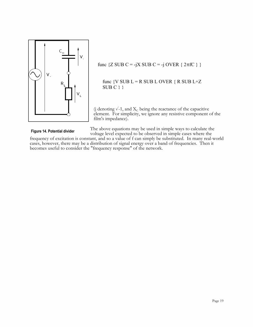
Page 19
(j denoting %-1, and XC being the reactance of the capacitive element. For simplicity, we ignore any resistive component of the film's impedance).
The above equations may be used in simple ways to calculate the voltage level expected to be observed in simple cases where the
frequency of excitation is constant, and so a value of f can simply be substituted. In many real-world cases, however, there may be a distribution of signal energy over a band of frequencies. Then it becomes useful to consider the "frequency response" of the network.
Figure 14. Potential divider
func {V SUB L = R SUB L OVER { R SUB L+Z SUB C } }
func {Z SUB C = -jX SUB C = -j OVER { 2BfC } }

Page 20
Frequency Response This is illustrated in the following example graphs. First, a lin/lin plot is shown (Figure 15, linear y-scale or amplitude, plotted against linear x-scale or frequency) with the corresponding phase plot (Figure 16) also shown in lin/lin form. Following these is a log/log plot (Figure 17), which will be dealt with in a little greater detail. Note that the phase curve indicates that at very low frequencies, the observed voltage will show significant phase deviation from the source (limiting at -90o or -B/2 radians at "dc" or zero Hz). The significance of this effect is great if the piezo film element is to be used as part of a control loop.
Figure 15. Magnitude response of R-C filter
Fi gu re
16 . P ha se
re sp on se
of
R- C filt
er
Figure 17. Magnitude response shown as log/log plot
+20 dB/decade
0.707
f(c)
(-3 dB)
(0 dB) Absolutely proportional-->
Propo
rtion
al to
rate
of c
hang
e

Page 21
Analysis of the log/log R-C frequency response curve Some key features: # the overall characteristic of this network is known as a high-pass filter # the frequency at which the magnitude falls to 0.707 or -3 dB is known as the "cut-off" or
"corner" frequency of the high-pass filter # this frequency can be calculated as f(c) = 1/(2BRC), when both the resistance R and capacitance
C are known # at frequencies well below the cut-off frequency, the plot has the form of a straight line with
gradient +20 dB/decade (in other words, doubling the frequency will double the signal amplitude) - this characteristic is identical with that of a differentiator network, and gives an output which is proportional to the rate of change of the input quantity
# at frequencies well above the cut-off frequency, the plot is level at "unity gain" and the output is
directly proportional to the input quantity # the filter characteristic can be approximated by these two intersecting straight lines, but the
magnitude actually follows an asymptotic curve, with magnitude -3 dB at the cut-off frequency where the straight lines cross
# the filter characteristic can then be applied to the frequency-domain description of any practical
signal by multiplying the filter transfer characteristic with the spectrum of the input signal, and deriving a response curve (output) which can in turn be transformed back into a time-domain signal.
Some practical examples of the effect of this filter characteristic will be shown next. For each signal, the time-domain description of the "perfect source" (e.g. the waveform which would be seen on an oscilloscope if the filter characteristic was absent) is given first, followed by its spectrum (obtained by use of the FFT [Fast Fourier Transform] algorithm supplied in the analysis software), then the filter characteristic (identical for all examples, but shown to emphasize the effect), then the resulting output signal spectrum obtained by multiplying the complex input spectrum by the complex filter characteristic, and finally the corresponding time-domain description obtained by inverse FFT, which shows the waveform an engineer would expect to observe in reality. Note: in Figures 15, 16 and 17 the R-C values used to generate the curve were R = 1MS
and C = 4.5 nF. In the following plots, the value of C was reduced to 1.5 nF. These values were chosen somewhat arbitrarily to demonstrate the principle, and so the scaling on the curves has not been annotated. But the time waveforms can be read in x units of seconds, and the frequency curves with x units of Hz. The cut-off frequency for R = 1MS and C = 1.5 nF is approximately 106 Hz.

Page 22
Key to following figures Figure 18 shows a relatively high-frequency sine wave passing through the network. In the
input spectrum, the signal is represented by a single spectral line at the appropriate frequency. This frequency is just below the filter "cut-off", and so is only slightly attenuated by the network. The resulting output wave is diminished in amplitude, and slightly shifted in phase.
Figure 19 shows the same process applied to a slower sine wave. In this case, the attenuation is
much greater, and the phase shift more significant. This situation occurs when trying to monitor steady vibration at "too low" a frequency using a piezo sensor. The phase behavior may be significant if a control loop is to be implemented.
Figure 20 shows a harmonic series, with a number of discrete spectral lines all lying below the
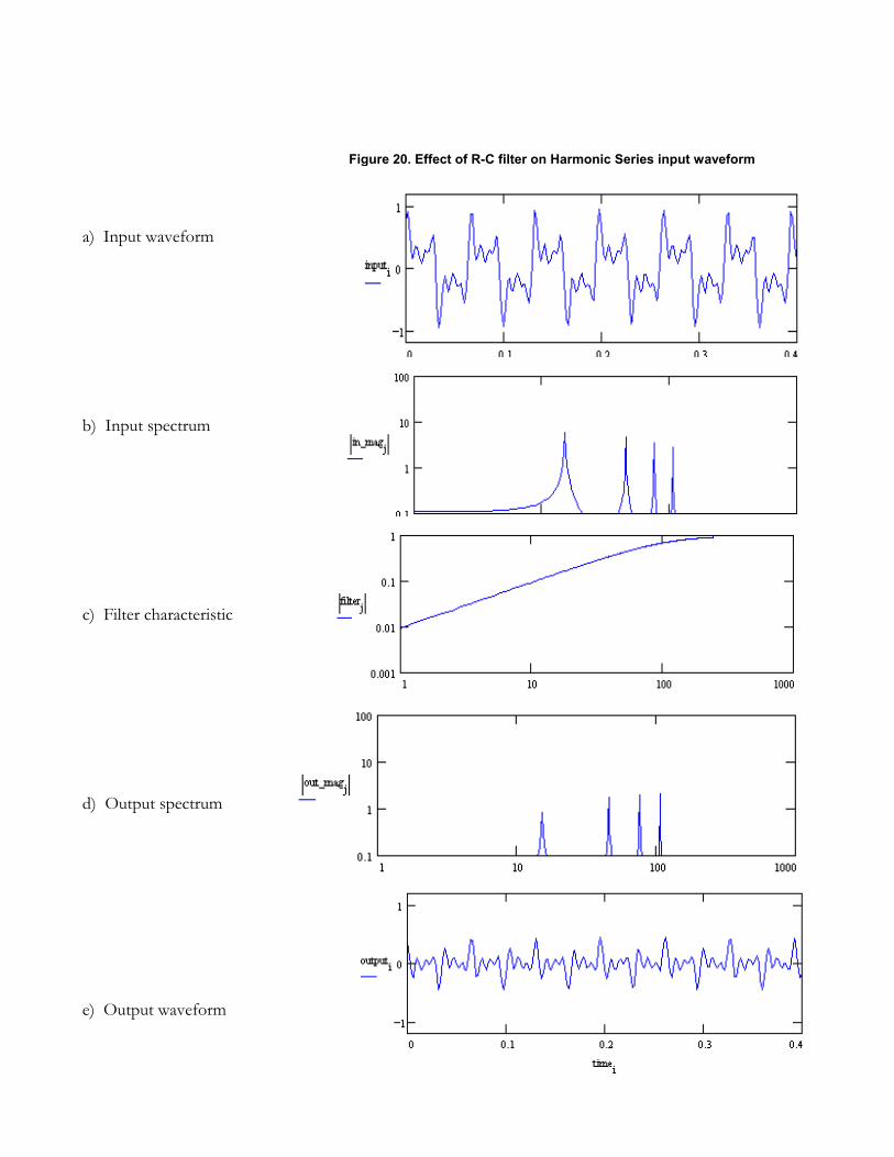
cut-off frequency. Each is attenuated to a different extent, and so the "balance" of harmonics in the output signal is altered.
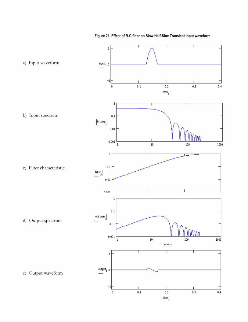
Figure 21 shows a slow half-sine input pulse (typical of many mechanical impact signals).
Although the high-frequency content is largely unaltered, the output waveform appears heavily "distorted" and clearly shows both positive and negative excursions, whereas the input waveform is unipolar.
Figure 22 shows a sawtooth waveform with slowly rising "leading edge" followed by a "snap"
descent back to zero. Many piezo switches detect this form of mechanical event. In the output waveform, the "leading edge" has almost disappeared, but the "snap" gives almost full amplitude. Note the polarity of the output pulse relative to the input waveform.

Page 23
a) Input waveform b) Input spectrum c) Filter characteristic d) Output spectrum e) Output waveform
Figure 18. Effect of R-C filter on High Frequency Sine Wave input waveform

Page 24
a) Input waveform b) Input spectrum c) Filter characteristic d) Output spectrum e) Output waveform
Figure 19. Effect of R-C filter on Low Frequency Sine Wave input waveform
Page 25
a) Input waveform b) Input spectrum c) Filter characteristic d) Output spectrum e) Output waveform
Figure 20. Effect of R-C filter on Harmonic Series input waveform
Page 26
a) Input waveform b) Input spectrum c) Filter characteristic d) Output spectrum e) Output waveform
Figure 21. Effect of R-C filter on Slow Half-Sine Transient input waveform

Page 27
a) Input waveform b) Input spectrum c) Filter characteristic d) Output spectrum e) Output waveform
Figure 22. Effect of R-C filter on Slow Sawtooth Transient input waveform

Page 28
TEMPERATURE EFFECTS Many of the properties of piezo film change with excitation frequency and temperature. These properties are reversible and repeatable with either frequency or temperature cycling. In addition, Figure 23 shows the permanent decay of the piezoelectric strain constant d33 for PVDF, annealed at 70oC, after long term exposure to elevated temperatures. Having reached a stabilizing temperature, the material properties then remain constant with time. Piezo film can be annealed to specific operating (or maximum storage) temperatures to achieve long-term stability for high temperature applications. Figure 24 shows the reversible temperature effects on d33 and g31 coefficients for PVDF. In Figures 25a and 25b, the effect of temperature on the dielectric constant (,/,O ) and dissipation factor (tan *e) are shown for copolymer films. Piezo films have been shown to offer excellent transducer properties at very low (cryogenic)
temperatures.
Figure 23. Thermal stability of d33 constant - 70EC annealed PVDF
Figure 24. Temperature coefficient for d33 and g31 constants - PVDF
Figure 25a. Dielectric loss tangent vs. temperature COPOLYMER
Figure 25b. Dielectric constant vs. temperature COPOLYMER

Page 29
PIEZOELECTRIC CABLE AND PROPERTIES One of the most recent developments in piezo polymer technology is piezo cable. The cable has the appearance of standard coaxial cable, but is constructed with a piezoelectric polymer insulator between the copper braid outer shield and the inner conductor (Figure 26). Protected by a rugged polyethylene jacket, the cable is used in buried or fence security systems, traffic sensors including vehicle classification and weight-in-motion systems, and taxiway sensors for aircraft identification, safety and security applications. Other applications include sensors for anti-tampering, door edge safety monitoring, floor mats, touch pads and panels, and patient mattress monitors. The new cables feature the same piezoelectric properties that are characteristic of piezo film sensors. The electrical output is proportional to the stress imparted to the cable. The long, thin piezoelectric insulating layer provides a relatively low output impedance (600 pF/m), unusual for a piezoelectric device. The dynamic range of the cable is substantial (>200 dB), sensing distant, small amplitude vibrations caused by rain or hail, yet responding linearly to the impacts of heavy trucks. The cables have withstood pressures of 100 MPa. The typical operating temperature range is -40 to +125EC. Table 4 lists typical properties for piezo cable. Table 4. Piezo Cable Typical Properties
Parameter Units Value
Capacitance @ 1KHz Tensile Strength Young's Modulus Density Acoustic Impedance Relative Permittivity tan *e Hydrostatic Piezo Coefficient Longitudinal Piezo Coefficient Hydrostatic Piezo Coefficient Electromechanical Coupling Energy Output Voltage Output
pF/m MPa GPa kg/m3 MRayl @1KHz @1KHz pC/N Vm/N Vm/N % mJ/Strain (%) kV/Strain (%)
600 60 2.3 1890 4.0 9 0.017 15 250 x 10-3 150 x 10-3 20 10 5
Figure 26. Piezo cable construction

Page 30
Cable Typical Properties The output sensitivity of piezo cable in response to increasing impact load is shown in Figure 27a. The linearity in output for increasing force as shown in Figure 27b is typical of all piezo cable gages.
PIEZOELECTRIC BASICS
Mechanical to Electrical Like water from a sponge, piezoelectric materials generate charge when squeezed. The amplitude and frequency of the signal is directly proportional to the mechanical deformation of the piezoelectric material. The resulting deformation causes a change in the surface charge density of the material so that a voltage appears between the electroded surfaces. When the force is reversed, the output voltage is of opposite polarity. A reciprocating force thus results in an alternating output voltage. Piezo film, like all piezoelectric materials, is a dynamic material that develops an electrical charge proportional to a change in mechanical stress. Piezoelectric materials are not suitable static measurements (true dc) due to their internal resistance. The electrical charges developed by piezo film decay with a time constant that is determined by the dielectric constant and the internal resistance of the film, as well as the input impedance of the interface electronics to which the film is connected. Practically speaking, the lowest frequency measurable with piezo film is in the order of 0.001Hz. There are methods to achieve true dc response, but these require using the piezo film as both an actuator and sensor, monitoring change in the actuation resulting from the dc event. The fundamental piezoelectric coefficients for charge or voltage predict, for small stress (or strain) levels, the charge density (charge per unit area) or voltage field (voltage per unit thickness) developed by the piezo polymer. Charge Mode:
Figure 27a. Sensitivity vs. load
Figure 27b. Piezo cable linearity
Sensitivity vs Load
Cha
rge/
Forc
eQ
/F (p
C/N
)
Peak Charge vs Stress
Cha
rge
Out
put (
nC)

Page 31
Under conditions approaching a short circuit, the generated charge density is given by: D = Q/A = d3nXn (n = 1, 2, or 3) The mechanical axis (n) of the applied stress (or strain), by convention, is: 1 = length (or stretch) direction 2 = width (or transverse) direction 3 = thickness direction where D = charge density developed Q = charge developed A = conductive electrode area d3n = appropriate piezoelectric coefficient for the axis of applied stress or strain n = axis of applied stress or strain Xn = stress applied in the relevant direction It is important to note that the d3n coefficient is commonly expressed in pico-Coulombs per Newton (pC/N), but the more correct form would be (pC/m2)/(N/m2) since the areas (m2) upon which the stresses or strains apply are very often different and cannot be "canceled". Voltage Mode: The open-circuit output voltage is given by: Vo = g3nXnt (n = 1, 2, or 3, as above) where g = appropriate piezoelectric coefficient for the axis of applied stress or strain Xn = applied stress in the relevant direction t = the film thickness Piezo Coefficients: The most widely used piezo coefficients, d3n and g3n, charge and voltage respectively, possess two subscripts. The first refers to the electrical axis, while the second subscript refers to the mechanical axis. Because piezo film is thin, the electrodes are only applied to the top and bottom film surfaces. Accordingly, the electrical axis is always "3", as the charge or voltage is always transferred through the thickness (n = 3) of the film. The mechanical axis can be either 1, 2, or 3, since the stress can be applied to any of these axes, as shown in Figure 28. Typically, piezo film is used in the mechanical 1 direction for low frequency sensing and actuation (< 100KHz) and in the mechanical 3 direction for high ultrasound sensing and actuation (> 100KHz).
Figure 28. Numerical classification of axes

Page 32
Directionality: Piezoelectric materials are anisotropic. This means that their electrical and mechanical responses differ depending upon the axis of applied electrical field or axis of mechanical stress or strain. Calculations involving piezo activity must account for this directionality. EXAMPLE 1:
A 1.45 psi load (10,000 N/m2) is applied to a piezo film switch of 2.54 cm length, 2.54 cm width and 110:m in film thickness. The switch element is rigidly backed, so the force acts to compress
the film's thickness (therefore g33 mode). In this example the load acts on the length by width area of the piezo film. The open circuit voltage developed across the thickness of the piezo film is:
where: V/m is Volts out per meter of piezo film thickness N/m2 is stress applied to the relevant film area. The conversion from psi to
N/m2 is approximately 7,000. EXAMPLE 2:
The same piezo film element as in EXAMPLE 1 is subjected to a force (10,000 N/m2 x 0.0254m2 = 6.45 Newtons), but in this example, the film switch is configured as a membrane having a
compliant backing. Now, the force acts on the thickness cross-sectional area (wt). The piezo film is being stretched by the load, so it is acting in the g31 mode.
The sharp increase in output voltage results because the force is applied to the much smaller cross-sectional area of the film. The small area results in a correspondingly higher stress.
func {horz 1000 LINESPACE 125 STACKALIGN {V_o`=&`-g_33`Xt # g_33`=&`-339`x`10^{-3}`{V/m} over {N/m^2}}}
func {horz 1000 LINESPACE 125 STACKALIGN {V_o`=&`-` left (-339`x`10^{-3} `{{V/m} over {N/m^2}} right )`(-10,000`N/m^2)(110`x`10^{-6}m) # VERT 3 V_o`=&`-0.373`\volts}}
func {horz 1000 linespace 125 stackalign {V_o`=&`-(`3g_31`left ( {F} over {wt}right )`(t)`=`-(g_31) left({F} over {w} right) # g_31`=&`216`x`10^{-3} {V/m} over {N/m^2} # V_o`=&`- left(216`x`10^{-3}{V/m} over {N/m^2} right )left ({6.45`N} over {2.54`x`10^{-2}m} right )# V o`=&`-54.9`\volts} }

Page 33
Dynamic Range Piezo film has a vast dynamic range. The sensor has been used to detect the impact of high speed particles in space having a mass of 10-12 grams, and at the other extreme, measures shock waves at 300,000 atmospheres produced during weapons testing. A recent study was conducted to determine the maximum output energy of a 52:m thick film, having an area of 155.5 mm x 18.5 mm. The film was subjected to approximately 350 MPa (in the stretch or "n = 1" direction) without failure. The charge generated was found to be very linear, with the following measurements made at maximum applied stress: Maximum Charge Observed: 20:C, giving 6.95 mC/m2 Maximum Voltage Observed: 1600 V, giving 30.8 x 10⁶ V/m Maximum Energy Converted: 30.9 mJ, giving 207 kJ/m3 Later experiments showed that about 10% of the above energy levels can be sustained for long periods of time without measurable damage to the piezo film element. Electrical to Mechanical When a voltage is applied to a sheet of piezo film, it causes the film to change dimensions due to the attraction or repulsion of internal dipoles to the applied field.. With one voltage polarity is applied, the piezo film becomes thinner, longer and wider. The opposite polarity causes the film to contract in length and width and become thicker. An ac voltage causes the film to "vibrate". The amount of deformation is given by the piezoelectric "d3n" constant: for length change where = change in film length in meters l = original film length in meters d31 = piezoelectric coefficient for length ("n=1" direction) change in meters per volt V = applied voltage across the thickness (t)
for width change where d32 = piezoelectric coefficient for width ("n=2" direction) change
for thickness change where
d33 = piezoelectric coefficient for thickness ("n=3" direction) change
f {
func { )w~
func { )t =

Page 34
EXAMPLE 3:
A piezo film of 3 cm length (l), 2 cm width (w) and 9:m thickness (t) is subjected to an applied voltage of V=200 volts in the 3 (thickness) direction. The amount of strain S resulting from this electrical input is d times the applied field.
In the l direction:
In the t direction: Actuators Generally, piezo film actuator designs depend on the application requirements such as operating speed, displacement, generated force, and available electrical power. Piezo film technology offers various design options to meet such application requirements. Those design options include: ! Customized electrode patterns on one or
both sides of the piezo film sheet. ! Multilaminate structures or bimorphs. ! Fold-over or scrolled multilayer
structures. ! Extruded piezo tubes and piezo cables. ! Cast piezo polymer on various substrates ! Molded 3-D structures. Each design option mentioned above has advantages and disadvantages. For example, scrolled multilayer actuators can generate a higher force but may sacrifice some displacement.
Figure 29. Piezo film bimorph
func {horz 1000 linespace 150 stackalign {S_1``=&``{DELTA`l`} over {l}``=``d_31`(V/t)~~ \where~d_31``=``23`x`10^{-12}`{m/m} over {V/m} # Horz 1 DELTA`l``=&``d_31(V/t)``l``=``\ left (23`x`10^{-12}`{m/m} over {V/m} right) {(200`V`)`(`3`x`10^{-2}`m)} over {(`9`x`10^{-6}`m`)} # Horz 1 DELTA`l``=&``1.53`x`10^{-5}`m~~\or~~15.3 ~mu m}}
func {horz 1000 DELTA`t``=``td_33(V/t)``l``=``d_33 V = left(-33`x`10^{-12}{m/m} over {V/m} right ) `left ( 200`V`right ) `=` 6.6`x`10^{-9}m ~\or~66D }
l t
w
x

Page 35
Bimorph Like a bimetal strip, two sheets of piezo film of opposite polarities, adhered together form a bending element, or "bimorph" (Figure 29). An applied voltage causes one film to lengthen, while the other contracts, causing the unit to bend. An applied voltage of opposite polarity bends the bimorph in the opposite direction. The bimorph configuration converts small length changes into sizable tip deflections, but producing low force. Thicker films and multilayers improve the force developed by the bimorph, but sacrifice displacement unless the unit can be operated at higher fields. The amount of tip deflection and the force developed are given by:
meters and
Newtons where )x = displacement at dc F = generated force d31 = piezoelectric coefficient in the "1" direction l,t,w = length, thickness, and width of piezo film V = applied voltage (Volts) Y = Young's modulus of piezo film (2x10⁹N/m2) By applying an ac voltage, the bimorph can act as a fan, similar to an insect wing. Although the piezo film bimorph does exhibit a dc response, maximum tip deflections are obtained when the unit is operated at resonance, determined by the length and thickness of the bimorph beam. EXAMPLE 4:
100 volts are applied across a 2 cm long cantilever bimorph comprised of two strips of 9 PVDF. The resultant tip displacement is:
As shown in the equations, more displacement can be obtained from a longer bimorph. Larger forces can be obtained from a wider bimorph. The ratio of displacement at a resonance frequency and dc is defined by Q which indicates a mechanical gain. A typical Q value for a piezo film bimorph is 20 to 25.
Figure 30. Lead attachment methods for a bimorph
func {horz 500 )x =
func {horz 500 F =
ffunc {horz 1000 linespace 150 stackalign {DELTA x``=&``{3/4Vd_31`l^2} over {t^2} # horz 1 DELTA x``=&``{{3/4(100`V) left(23`x`10^{-12}`{{m/m} over {V/m}} right)`(2`x`10^{-2}``m)^2} over {(9`x`10^{-6}``m)^2}} # horz 1 DELTA x``=&``8.52 mm}}
SERIES
PARALLEL
VOLTAGESOURCE
VOLTAGESOURCE

Page 36
For example, a 5 mm long 70:m thick bimorph with 120 volts dc creates a displacement of 57:m. With the same bimorph, however, displacement can be 1.4 mm at the resonant frequency of 580 Hz. For applications that require a higher force, such as cooling fans, multilayer construction can be considered. The resulting output force is proportionally increased by the number of layers. In terms of electrical connections to the bimorph, there are two basic methods as shown in Figure 30 — parallel and series connections. In order to generate the same amount of displacement, the parallel connection requires a lower voltage than the series connection. Series connections, on the other hand, draw less current than parallel connections. For both parallel and series connections, the total electrical power to the actuator is identical. However, it is obvious that the lead attachment of the series connection is much simpler than that of the parallel connection for manufacturing purposes. Typical applications of the bimorph bender are cooling fans, toys, and decoratives. Scrolled Actuator
The generated force and displacement of a scrolled piezoelectric cylinder in Figure 31 are expressed as follows: Meters
Volts/meters
Newtons where
x = displacement at dc (meter) F = generated force (Newton) f = resonance frequency l,t = Length, thickness of piezo film (meters) Me = externally loaded mass (kilograms) Mp = piezo actuator mass (kilograms) A = cross sectional area (m2) Y = Young's modulus (N/m2) E = electrical field (volt/meter) As shown in the equations, a scrolled actuator can generate more force and can respond with a higher resonant frequency by increasing the cross sectional area. A longer actuator generates more displacement but reduces the response speed. Note that the actuator output, with Me = 0, will be maximized when the length l is adjusted to satisfy the resonant condition. As an example, the performance of a 12 mm diameter, 25 mm long scrolled actuator can be maximized at 32 KHz operation. Folded Actuator
Figure 31. Scrolled piezo film actuator
func {horz 200 x``=``d_{31}El}
ffunc {horz 200 F``=``Yd_31EA}
func {horz 200 f``=``(1/2 pi) SQRT {Y`A/l`(M_e`+`0.405`M_p)}}
DISPLACEMENT (X)FORCE (F)
CROSS SECTIOAREA (A)
VOLTAGESOURCE
STR
ETC
H D
IRE
CTI
ON

Page 37
Another design option for a high speed, high force actuator is to fold over a long sheet of piezo film as shown in Figure 32. This design effectively creates a parallel wired stack of piezo film discs. The center hole is used to secure the actuator to a base. Design equations of the scrolled actuator also can be applied to this type of actuator. In the previous equations, d31 should be replaced with d33 (-33x10-12 C/m2) for a folded actuator. An example of specifications for the folded actuator is shown below: Displacement: 1 :m/1 mm length Generated force: 15 kg/10 mm dia. Frequency: dc - 100 kHz Drive voltage: 800 volts

Page 38
Compared to mechanical or piezo ceramic actuators, multilayer piezo film actuators have fewer ringing problems due to their lower Q. Applications of multilayer actuators are micropositioners for industrial equipment, acoustic wave generators and ink jet printers. Ultrasonic Actuators Ultrasonic actuators, as discussed in this section, exclude very high frequency (> 1 MHz) transmitter applications. The use of piezo film in these very high frequency applications, like medical ultrasound imaging and nondestructive testing, use thickness mode operation, d33.This section deals with low frequency ultrasound (20-100 KHz) where the piezo film can be used in the length change (d31) mode. The advantage of piezo film in low frequency ultrasound can be found from the flexibility of the material. Piezo film can be easily curved or formed to make circular transducers as shown in Figure 33. The beam pattern is determined by the number of half circular elements and their diameter. The operating frequency is determined by the diameter of the half circular elements. Note that the difference between Figures 33(a) and 33(b) is their number of active elements and diameters. To widen the beam coverage, the number of active elements should be reduced. With a cylindrical transducer, a 360o beam pattern is obtained. In ultrasound applications, a narrow beam with minimum side lobes is required for remote distance measurements. On the other hand, a wide beam, as wide as 180o or more, is required for applications like automobile rear bumper proximity sensing. Figure 33 shows design configurations for both narrow beam and wide beam ultrasound transducers.The applications for piezo film in through-air ultrasonic actuators include distance ranging for air pen, air mouse, white board digitizer, collision avoidance, physical security systems, air flow velocity (doppler) sensors, and inter-object communications. Similar constructions can be produced for underwater or fluid sensing, including flow sensors, level sensors, and communications. PYROELECTRIC BASICS Piezoelectric polymers, such as PVDF and its copolymers of VF2/VF3, are also pyroelectric. Pyroelectric sensor materials are normally dielectric materials with a temperature-dependent dipole moment. As these materials absorb thermal energy, they expand or contract, thereby inducing secondary piezoelectric signals. As piezo film is heated, the dipoles within the film exhibit random motion by thermal agitation. This causes a reduction in the average polarization of the film, generating a charge build up on the film surfaces. The output current is proportional to the rate of temperature change ()T). The amount of electrical charge
Figure 32. Folded piezo film actuator
Figure 33. Piezo film ultrasound transducers
PIEZO FILMELECTRODE
FOLD LINE
PIEZO FILM PATTERN
DISPLACEMENT (X)FORCE (F)
MOUNTING HOLE
FOLDED PIEZO FILM STACK
THICK METALELECTRODES
Piezo Film
Piezo Film
Plastic Base
Plastic Base
Beam Pattern
Beam Pattern
(b) Wide Beam Transducer
(a) Narrow Beam Transducer

Page 39
produced per degree of temperature increase (or decrease) is described by the pyroelectric charge coefficient, D. The charge and voltage produced in a given film of area A permittivity ,, and thickness t is given by: EXAMPLE 5:
A piezo film pyroelectric detector having a film thickness (t) of 9:m, a permittivity (,) of 106x10-
12 C/Vm and a pyroelectric coefficient (p) of 30x10-6 C/(m2oK), undergoes a temperature increase
()T) of 1oK due to incident IR radiation. The output voltage is given by: The pyroelectric voltage coefficient of piezo film is about an order of magnitude larger than those of Lead Zirconate Titanate (PZT) and Barium Titanate (BaTiO3). Table 5 compares the pyroelectric properties of these materials, but a far lower figure of merit due to the low capacitance of PVDF. Table 5. Comparison of pyroelectric materials
Material TGS LiTaO3 BaTiO3 PZT PbTiO3 PVDF VF2VF3
func { 350 200 400 420 230 30 50
, `/` , 30 45 1000 1600 200 10.7 8.0
" .16 1.31 1.00 .44 .67 .06 .06 L 225 646 564 374 461 138 138 Pv 1.32 .50 .05 .03 .10 .47 .71 Ml .53 .16 .02 .01 .03 .20 .31
Pyroelectric Charge Coefficient (DQ):Coul/[m2•EK] Dielectric Constant func {(,/, o), where~ , o =Thermal Diffusivity (")m2/sec •10-6 Thermal Diffusion Depth @ 1Hz (L):m Pyroelectric Voltage Coefficient (PV)DQ/,, V/[:m•EK] Figure of Merit (Ml)DQ/[CV •,], V •mm2/J
func {linespace 150 stackalign {Q``=&``p DELTA`TA # V``=&``pt DELTA`T/,}}
func {horz 1000 linespace 150 stackalign {V``=&``{(30`x`10^{-6}`C/m^2` DEG K)(9`x`10^{-6}m)(1 DEG K)} over {(106`x`10^{-12}`C/Vm)} # horz 1 V``=&``2.55~\volts }}
Page 40
Piezo film advantages including: — moisture insensitivity (<.02% H2O absorption) — low thermal conductivity — low dielectric constant — chemical inertness — large detector sizes The pyroelectric response of piezo film can also become a noise source for piezo sensor applications at low frequencies. In piezoelectric applications where low frequency strain sensing is desired, there are several convenient methods to “common-mode reject” the pyroelectric response. Examples include: ! Two equal sized electrode patterns on one piezo film element; one electrode oriented parallel
to the d31 and the other electrode pattern is perpendicular to the d31 direction. Both develop equal signals in response to pyro, but the electrode area parallel to the d31 develops about 10X the perpendicular electrode pattern. Subtracting the signals yields a pure piezo response.
! Two equal sized piezo film elements, laminated in a stacking configuration; one film has d31 parallel to strain surface, the other has d31 perpendicular to strain surface. As above, signals are subtracted to isolate the piezo response from pyro.
! Several other common mode rejection techniques can be described by MSI’s applications engineers.
For higher frequencies, where the rate of temperature change seen by the piezo film element is slower than the strain event to be measured, frequency filters readily sort out the unwanted pyro signal. BASIC CIRCUIT CONCEPTS A properly designed interface circuit plays a key role in the optimization of piezo film sensors. The applications of piezo film span from toys to military sensors and interfacing to electronics is highly application dependent. In many cases, piezo film can be directly connected to electronic circuits without special interface considerations. However, for those cases where an interface circuit is required, the following 3 steps are recommended: 1. Consider the frequency range and signal amplitude requirements over the desired dynamic
range. 2. Choose a proper load resistance to assure the
low end operating frequency and to minimize signal loss due to the loading effect.
3. Select a buffer circuit if the signal level is small. If a high value load resistance is needed (such as 22MS or higher value), a low leakage high impedance buffer amplifier is recommended. JFET's or CMOS operational amplifiers are commercially available for a buffer.
Simplified Equivalent Circuits
Figure 34. Equivalent circuit of piezo film
Page 41
The first step in an interface circuit design is to understand the piezo film characteristics as part of an electrical equivalent circuit. Figure 34 shows a simplified equivalent circuit of piezo film. It consists of a series capacitance with a voltage source. The series capacitance Cf represents piezo film capacitance which is proportional to the film permittivity and area and inversely proportional to film thickness. The voltage source amplitude is equal to the open circuit voltage of piezo film and varies from microvolts to 100's of volts, depending on the excitation magnitude. This simplified equivalent circuit is suitable for most applications but is of limited value at very high frequencies such as that used in ultrasound transducers. Figure 35 shows an equivalent circuit as a charge generator. This equivalent circuit has film capacitance Cf, and internal film resistance Rf. The induced charge Q is linearly proportional to the applied force as described earlier. The capacitance Cf is proportional to the surface area of film and is inversely proportional to the film thickness. In low frequency applications, the internal film resistance Rf is very high and can be ignored. The open circuit output voltage can be found from the film capacitance; i.e., V=Q/Cf. Input Resistance The most critical part of an interface circuit is the input resistance. The input resistance affects low frequency measurement capability as well as signal amplitude. This is called the "loading effect". Piezo film capacitance can be regarded as an equivalent source impedance. It is important to note that this source
impedance increases with decreasing film capacitance and decreasing frequency of operation. This source impedance combined with the input resistance produces a voltage divider. As the ratio of input resistance to source impedance is decreased, the overall output voltage is reduced.
Therefore, choosing a proper input resistance for the electronic interface is critical in minimizing the loading effect.
Figure 35. Equivalent circuit for piezo film
Figure 36. Equivalent circuit of piezo film with input resistance of electronic interface
Figure 37. Time response of piezo film
Page 42
Time Constant In addition to input resistance, the input capacitance of an interface circuit can also affect the output. Figure 36 shows the equivalent circuit of film with input resistance Ri and input capacitance Ci. A typical time domain response of piezo film is shown in Figure 37 . The charge developed on the film due to an applied force decays with a time constant which is defined by Ri(Cf + Ci). This time constant represents the time required for a signal to decay to 70.7% (-3dB) of its original amplitude. The smaller the time constant, the quicker the signal decays. Because of this finite time constant, piezo film is suitable for dynamic measurements rather than static measurement (0.001 Hz minimum). If a long time constant is desired, a high input resistance and film capacitance can be used. It should be understood, however, that a high input resistance can also produce higher noise, requiring compensation through shielding, etc. Frequency Response

Page 43
Another important aspect of the time constant can be seen in the frequency response of the equivalent circuit. The circuit exhibits an RC high-pass filter characteristic as shown in Figure 38. In this figure, the vertical axis implies the ratio of observable output signal to the developed signal (open circuit voltage of the piezo film). Zero dB implies no loss of signal. The cutoff frequency (3 dB down) is inversely proportional to the time constant. When a piezo film sensor is operated below this cut-off frequency, the output signal is significantly reduced. For a low frequency measurement, an input resistance needs to be high enough so that the cut-off frequency is well below the desired operating frequency. This consequence can be verified from consideration of the time constant as well as the loading effect.
Figure 38. High pass filter characteristic of piezo film

Page 44
As an example, the frequency response of a shielded piezo film sensor (model SDT1) is shown in Figure 39. In this example, the SDT is interfaced with a circuit which contains a 10MS load resistor and an FET. The capacitance of the piezo film is 2.4 nF. With 10MS load resistance, the time constant becomes 24 msec and thus, the cut-off frequency is 6.6 Hz. For comparison, the cut-off frequency can be reduced to 0.66 Hz if a 100MS resistor is used instead of the 10MS resistor. This sensor component can be used for any application operating above the cut-off frequency determined by the resistance value. In applications where the electronic circuit cannot be placed near the sensor, a buffer circuit is recommended close to the sensor. The buffer circuit converts the high output impedance of the piezo film element into a low output impedance and thus minimizes the signal loss and noise through the cable. For large size (i.e., high capacitance) piezo film sensors a buffer may not be required, even with small signals and long cables. When a high piezo film output impedance is required, a low-leakage, high impedance buffer is necessary. For example, infrared motion sensor and accelerometer applications require up to 50GS of input resistance to obtain a very low frequency response. For such cases, the input impedance of the buffer must be much higher than the output resistance of the piezo film in order to maintain the low frequency response. In addition, minimum leakage current of the buffer is critical in order to maximize the measurement accuracy. Some examples of low leakage buffer electronics include: JFET - 4117 (Siliconix, Sprague); Operational amplifiers — LMC660, LF353 (National Semiconductor), OP80 (PMI), and 2201 (Texas Instruments). Figure 40 shows unity gain buffer circuit examples for general applications. Operational amplifiers offer a great deal of versatility as both buffers and amplifiers. They can be used as either charge-mode or voltage-mode amplifiers. Figure 41 shows basic charge and voltage amplifier configurations. The voltage output of the charge
Figure 39. Frequency response of SDT1
Figure 40. Unity gain buffer for piezo film sensors
Figure 41. Typical amplifiers for piezo film sensors

Page 45
amplifier is determined by Q/Cf. Q is the charge developed on the piezo film and Cf is the feedback capacitance of the charge amplifier. The output voltage of the charge amplifier depends on the feedback capacitance, not the input capacitance. This indicates that the output voltage of a charge amplifier is independent of the cable capacitance. The major advantage of a charge amplifier can be realized when a long cable is used between a piezo film sensor and electronics. In addition, it also minimizes charge leakage through the stray capacitance around the sensor. Otherwise, simple voltage amplifiers are sufficient for most applications. Included in Figure 41 is a typical non-inverting voltage amplifier. The advantage of a voltage amplifier can be seen when ambient temperature is considered. The voltage sensitivity (g-constant) variation over temperature is smaller than the charge sensitivity (d-constant) variation. Consequently, voltage amplifiers with piezo film exhibit less temperature dependence. In Figure 41, the time constants for the charge amplifier and voltage amplifier are determined by RCf and RC respectively. As a design example, a traffic sensor interface is described. Because of its flexibility, piezo cable is an ideal sensor material for traffic measurement applications. MSI’s BL traffic sensor is constructed with a piezo cable sheathed in a compressed brass tube, with a variety of signal cable lengths tailored to the installation requirements. The BL is available in sensing lengths of more than 3 meters. In this specific example, the BL sensor is 2 meters long. This electrically shielded sensor has 100 feet of coax cable. The electrical specifications of this sensor include: Capacitance = 9.5 nF (including piezo cable and signal cable capacitances)
Output = 500mV (for a wheel load of 800 pounds at 55mph and 70°F) Signal : Noise = 10:1
The basic requirements of an interface circuit are: Low end frequency = 1.6 Hz Circuit output = Digital pulse count An interface circuit to meet these requirements is shown in Figure 42. This circuit works as a comparator. A 10MS input resistance is chosen in order to reduce the cut-off frequency to about 1 Hz. The actual cut-off frequency with this resistor can be calculated as 1.6 Hz. A 10MS potentiometer is used to adjust the threshold voltage, V and the diode is included to protect the electronics from high voltage damage. Typical piezo film and interface circuit output signals from a passenger car at 55 mph are shown in Figure 42.

Page 46
Figure 42. An interface circuit of a traffic sensor

Page 47
Signal Conditioning Because piezo film is both piezoelectric and pyroelectric, some provision must be made to eliminate—or at least reduce—the effect of unwanted signals. The primary principles of signal conditioning include: • Filtering—Electrical filters designed to give the desired band-pass and band-rejection characteristics. • Averaging—If the desired signal exhibits periodicity, while the undesired signal is random, signal averaging can increase the signal-to-noise ratio. • Common Mode Rejection—By wiring two equal areas of a piezo film electrode out-of-phase, unwanted common-mode signals can be made to cancel. Basic Switch Circuitry A variety of circuits are available to electronically interface with piezo film including field effect transistors (FETs), operational amplifiers (Op Amps), and low-current digital logic (CMOS). FETs lend themselves to applications of small size since they are readily available in surface mount technology. Important characteristics to consider when using FETs are switching frequency, piezo film capacitance, leakage current of the FET in the off-state, input bias resistance, and shielding from electromagnetic interference (EMI). Figures 43 and 44 show typical FET circuit configurations for a piezo film switch. Figure 43, the common drain or source follower, applies well in applications where simple buffering is important. Here, the circuit voltage gain is approximately one. The common source circuit in Figure 44 is suitable for low frequency applications where voltage gain is required. The gain is determined by resistances RD and RS. As the gain increases, frequency bandwidth decreases by a factor of one decade per 20 dB of gain. Operational amplifiers offer a great deal of versatility for piezo film switch applications. Adaptation to a particular application is often as simple as making a few wiring changes. Important op amp circuit characteristics include input bias resistance, film switch capacitance, and EMI shielding. The op amp circuit of Figure 45, a charge amplifier, suits applications where a detected vibration actuates the switch. It also works well in small signal applications. A charge amplifier eliminates the effects of the time constants of both the piezo film and
Figure 43. High frequency, low gain FET circuit interface
Figure 44. Low frequency, high gain FET circuit interface
Figure 45. Op Amp Interface circuit acting as a charge amplifier
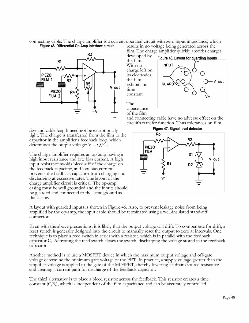
Page 48
connecting cable. The charge amplifier is a current operated circuit with zero input impedance, which results in no voltage being generated across the film. The charge amplifier quickly absorbs charges developed by the film. With no charge left on its electrodes, the film exhibits no time constant. The capacitance of the film and connecting cable have no adverse effect on the circuit's transfer function. Thus tolerances on film
size and cable length need not be exceptionally tight. The charge is transferred from the film to the capacitor in the amplifier's feedback loop, which determines the output voltage: V = Q/Cf. The charge amplifier requires an op amp having a high input resistance and low bias current. A high input resistance avoids bleed-off of the charge on the feedback capacitor, and low bias current prevents the feedback capacitor from charging and discharging at excessive rates. The layout of the charge amplifier circuit is critical. The op-amp casing must be well grounded and the inputs should be guarded and connected to the same ground as the casing. A layout with guarded inputs is shown in Figure 46. Also, to prevent leakage noise from being amplified by the op-amp, the input cable should be terminated using a well-insulated stand-off connector. Even with the above precautions, it is likely that the output voltage will drift. To compensate for drift, a reset switch is generally designed into the circuit to manually reset the output to zero at intervals. One technique is to place a reed switch in series with a resistor, which is in parallel with the feedback capacitor Cf. Activating the reed switch closes the switch, discharging the voltage stored in the feedback capacitor. Another method is to use a MOSFET device in which the maximum output voltage and off-gate voltage determine the minimum gate voltage of the FET. In practice, a supply voltage greater than the amplifier voltage is applied to the gate of the MOSFET, thereby lowering its drain/source resistance and creating a current path for discharge of the feedback capacitor. The third alternative is to place a bleed resistor across the feedback. This resistor creates a time constant (CfRf), which is independent of the film capacitance and can be accurately controlled.
Figure 46. Layout for guarding inputs
Figure 47. Signal level detector
Figure 48. Differential Op Amp interface circuit
Page 49
The signal level detector of Figure 47 fits applications where large signal-to-noise ratios are desirable. This circuit is perfect for detecting an impact among low-level vibrations. For situations where signal to noise ratios are low and where impacts or pressures must be discerned from background vibration, the differential amplifier circuit of Figure 48 is appropriate. This circuit consists of two sensors driving a differential amplifier.

Page 50
This configuration uses a common-mode rejection concept. The two switches are mechanically coupled to cancel unwanted vibrations that stimulate both. An input or pressure on one switch but not the other, will produce an output. CMOS logic offers a low-cost way to interface with piezo film. As mentioned earlier, low-power circuits implemented with CMOS technology are ideally suited to piezo film switches. CMOS applications for piezo film are generally for low frequency operation. Other characteristics to consider include device input leakage current and input impedance, input bias resistance, and the effect of EMI. A CMOS circuit can be used, for example, in applications to sense a single impact or a single pressure. The D-Flip Flop in Figure 49 indicates the presence of either the impact or pressure to set off an audible alarm. The circuit in Figure 50, senses multiple impacts or pressures for counting applications. Many different CMOS circuit configurations are possible to interface with piezo film. Common to all of them is an input bias resistor in parallel with the piezo film, and an input resistor in series with the film. The bias resistor handles leakage current and the series resistor limits current to protect against electrostatic discharge. Cables In applications where it is not possible to place the amplification circuit in close proximity to the piezo film transducer, considerable care must be exercised in selecting the connecting cable that carries the high-impedance signal. Shielded coaxial cable, while used for noise reduction, can add problems associated with cable leakage and added capacitance. In most cases the cable's primary insulation should consist of highly resistant, non-polar plastics such as high-purity polyethylene or Teflon® (PTFE). It is equally important to make the cable as vibration-free as possible since cable movements generate noise that interferes with signal transmission.
Figure 49. CMOS circuit for detecting a single impact
Figure 50. CMOS interface circuit for counting applications

Page 51
MANUFACTURING Rolls of piezo film are produced in a clean room environment The process begins with the melt extrusion of PVDF resin pellets into sheet form, followed by a stretching step that reduces the sheet to about one-fifth its extruded thickness. Stretching at temperatures well below the melting point of the polymer causes chain packing of the molecules into parallel crystal planes, called “beta phase”. To obtain high levels of piezoelectric activity, the beta phase polymer is then exposed to very high electric fields to align the crystallites relative to the poling field. Copolymers of PVDF are polarizable without stretching. Evaporatively deposited metals are typically 500 to 1000 Å in thickness, and almost any metal can be deposited. Popular metals are nickel, aluminum, copper, gold and alloys . Electrode patterns are made by sputtering through masks or by chemical etching continuous metallizations using photoresists. Resolution to 25:m line widths has been achieved. Screen printed electrodes of conductive silver ink are much thicker, about 5-10 :m, and can be applied in complex patterns to form multiple sensors on a single sheet. Foils are adhered with thin adhesive layers and capacitively coupled to the piezo film. Each electrode alternative has advantages and disadvantages. Generally, sputtered metals are for very high resolution arrays, pyroelectric applications requiring a low thermal mass, or for inertness, as with invasive medical applications. Fully metallized sheets can by carefully cut with a razor blade without shorting across the film thickness. Screened inks are very robust and compliant, withstand very high strains (>10%), can operate at high voltages without breakdown, and are easy to pattern on a continuous basis. However, unmetallized borders are required for cutting elements out of a sheet of screen printed electrodes, since there is a high likelihood of shorting across the films thickness with the thick inks. Foils may mechanically restrict the piezo film from responding to externally applied stresses and strains in the plane of the film, but foils are useful in pure "thickness mode" operation. After metallization, a wide variety of possible processing steps are followed to produce a packaged sensor. Generally, the piezo film is laminated in a protective carrier film, die cut to size, and packaged with lead wires or crimp connectors and, often, signal conditioning electronics. The wide range of packaged sensors, from a few square millimeters (including an ASIC chip) as a shipping damage sensor, to multiple square meter sensors for sports scoring targets suggests the versatility of this technology. APPLICATIONS The sensor applications described below represent a good cross-section of the products now using piezo film sensors. Switches The reliability of contact switches is reduced due to contaminates like moisture and dust which foul the contact points. Piezo film offers exceptional reliability as it is a monolithic structure, not susceptible to this and other conventional switch failure modes. One of the most challenging of all switch applications is found in pinball machines.
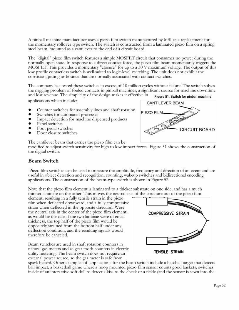
Page 52
A pinball machine manufacturer uses a piezo film switch manufactured by MSI as a replacement for the momentary rollover type switch. The switch is constructed from a laminated piezo film on a spring steel beam, mounted as a cantilever to the end of a circuit board. The "digital" piezo film switch features a simple MOSFET circuit that consumes no power during the normally-open state. In response to a direct contact force, the piezo film beam momentarily triggers the MOSFET. This provides a momentary "closure" for up to a 50 V maximum voltage. The output of this low profile contactless switch is well suited to logic-level switching. The unit does not exhibit the corrosion, pitting or bounce that are normally associated with contact switches. The company has tested these switches in excess of 10 million cycles without failure. The switch solves the nagging problem of fouled contacts in pinball machines, a significant source for machine downtime and lost revenue. The simplicity of the design makes it effective in applications which include: ! Counter switches for assembly lines and shaft rotation ! Switches for automated processes ! Impact detection for machine dispensed products ! Panel switches ! Foot pedal switches ! Door closure switches The cantilever beam that carries the piezo film can be modified to adjust switch sensitivity for high to low impact forces. Figure 51 shows the construction of the digital switch. Beam Switch Piezo film switches can be used to measure the amplitude, frequency and direction of an event and are useful in object detection and recognition, counting, wakeup switches and bidirectional encoding applications. The construction of the beam-type switch is shown in Figure 52. Note that the piezo film element is laminated to a thicker substrate on one side, and has a much thinner laminate on the other. This moves the neutral axis of the structure out of the piezo film element, resulting in a fully tensile strain in the piezo film when deflected downward, and a fully compressive strain when deflected in the opposite direction. Were the neutral axis in the center of the piezo film element, as would be the case if the two laminae were of equal thickness, the top half of the piezo film would be oppositely strained from the bottom half under any deflection condition, and the resulting signals would therefore be canceled. Beam switches are used in shaft rotation counters in natural gas meters and as gear tooth counters in electric utility metering. The beam switch does not require an external power source, so the gas meter is safe from spark hazard. Other examples of applications for the beam switch include a baseball target that detects ball impact, a basketball game where a hoop mounted piezo film sensor counts good baskets, switches inside of an interactive soft doll to detect a kiss to the cheek or a tickle (and the sensor is sewn into the
Figure 51. Switch for pinball machine
Figure 52. Beam switch
CANTILEVER BEAM
PIEZO FILM
CIRCUIT BOARD

Page 53
fabric of the doll), coin sensors for vending and slot machines and as digital potentiometer for high reliability. Snap-Action Switches Piezoelectric materials do not have a true dc response. Very slow events, 0.0001 Hz, for example, are not normally possible to detect with piezoelectric film. In switch applications where dc response is required, piezo film in combination with a snap dome provides a high voltage pulse. When the snap device actuates, the film is rapidly strained, typically generating a 10 volt pulse into a one megohm circuit as shown in Figure 53. This concept is especially well suited for wakeup switches, where an electronic device can be dormant for long periods without power consumption until the snap action device is actuated. The piezoelectric pulse turns on the electronics. Battery operated parking meters, where battery life is very critical, are an example of a piezo snap action switch application. A thermal snap action device also employs this principle. Impact Sensors Impact Printers High speed impact printers require very accurate print head timing. Impact must occur the instant that a high speed revolving steel band, embossed with print characters, is properly positioned in front of the print hammer. Any advance or delay in energizing the print hammer will result in an offset print of the desired character. Piezo film sensor strips, built into the printer platen, monitor the impact timing and force of the bank of print heads, and transmit the information to the controller. Automatic adjustment is made in the actuator timing to accommodate any minor change in print head timing. The very high speed of the embossed steel ribbon, about 300 inches per second, requires a very fast switch response. Alternative impact switches are quickly destroyed by the large impact forces of the print head. Piezo film switches have been in use in this application for more than five years without failure. Sports Scoring Piezo film sensors can be used to measure impact time, location (accuracy) and force. These parameters are desirable in several sports scoring applications. The energy of a 90 mph pitch has instantaneous power of about 50,000 watts! The great challenge in this application is target ruggedness without the introduction of severe bounceback into the design. A second sports scoring application is electronic dartboards, where piezo film monitors the many impact zones in the game. Scoring is electronically recorded. Musical Instruments
Figure 53. Snap-action switch

Page 54
The popularity of electronics for musical instruments presents a special problem in drums and pianos. The very high dynamic range and frequency response requirements for drum triggers and piano keyboards are met by piezo film impact elements. Laminates of piezo film are incorporated in foot pedal switches for bass drums, and triggers for snares and tom-toms. Piezo film impact switches are force sensitive, faithfully duplicating the effort of the drummer or pianist. In electronic pianos, the piezo film switches respond with a dynamic range and time constant that is remarkably similar to a piano key stroke. The U.S. Government is actively studying "smart highways" as an alternative to major new highway construction. The idea is that existing highways can accommodate greater vehicle densities if electronically managed. In addition to conventional traffic monitoring for highway studies and enforcement, the Intelligent Vehicle/Highway System (IVHS) programs create the need for new classes of "smart highway" high speed sensors to count and classify vehicles, provide lane control, and to monitor weight and speed. IVHS also requires "smart car" sensors, and advanced vehicle surveillance, communications, and software. Futuristic programs like the IVHS, and more contemporary projects like the Strategic Highway Research Program (SHRP), require traffic data collection to provide the necessary information required by the Federal Highway Administration on highway structures. Recent advancements in signal processing open the door to greatly improved real-time vehicle data analysis, provided that inexpensive reliable sensor technologies are developed. Pneumatic road tubing has long been the workhorse of traffic data collection. Road tubes provide a pneumatic pulse to a piezoelectric membrane, which triggers nearby electronics when an axle is detected. The evaluation of alternative sensor technologies has shown piezo cable provides the necessary sensitivity, linearity, noise immunity and environmental stability for high traffic interstate vehicle
Figure 54. Permanent In-The-Road Traffic Sensor
Figure 55. Permanent, In-The-Road Traffic Sensor

Page 55
classification and weight-in-motion systems. Piezo cable BL sensors are used for traffic data collection from Saskatchewan to Florida. Piezo cable traffic sensor constructions are shown in Figures 54 and 55. There are two basic categories of traffic sensor ... permanent and temporary. Generally, permanent sensors are mounted in the road with the top of the sensor flush to the highway surface, while temporary units are adhesively applied to the road surface for shorter monitoring periods. Permanent sensors, used for toll booths and interstate highway data collection, are flush mounted to a road surface and must withstand the rigors of years of high density traffic, snow plows, salt, sand, water and dragging mufflers. Traffic sensors can monitor vehicle speed, count axles, weigh vehicles, provide direction, and vehicle classification. Recently, these sensors have also proven valuable on airport taxiways. From the output, one can discern the ground speed of an aircraft (time lag between two sensors), its direction, weight (fueled), number of axles, and the span of the aircraft (determined from the speed and the known fixed distance between sensors). This information can be used to classify the aircraft and provides taxiway traffic control and safety information at airports. VIBRATION SENSING One of the first applications for piezo film was as an acoustic pickup for a violin. Later, piezo film was introduced for a line of acoustic guitars as a saddle-mounted bridge pickup, mounted in the bridge. The very high fidelity of the pickup led the way to a family of vibration sensing and accelerometer applications. Music Pickups Piezo film is used today in several guitar pickup designs; one is a thick film, compressive (under the saddle) design; another is a low cost accelerometer, while another is an after market pickup design that is taped to the instrument. Because of the low Q of the material, these transducers do not have the self-resonance of hard ceramic pickups. Shielding can be achieved by a foldover design as shown in Figure 57. The hot side is the slightly narrower electrode on the inside of the fold. The foldover technique provides a more sensitive pickup than alternative shielding methods because the shield is formed by piezoelectric material. Conventional shielding laminates can be easily fabricated by a multilayer laminate of piezo film, adhesive and shielding foil.
Figure 57. Shielding piezo film

Page 56
Machine Monitoring The fidelity of a shielded piezo film sensor in musical instruments led to the development of vibration sensors for machines. In its simplest mode, piezo film vibration sensors behave essentially like dynamic strain gages. The film does not require an external power source, yet typically generates signals greater than strain gages after amplification. A typical piezo film sensor produces four orders of magnitude higher voltage signal than a foil-type strain gage, and two orders higher than semiconductor types. The frequency response of the piezo film strain gage is also superior. The extreme sensitivity is due to the form of the piezo film material. The low thickness of the film results in a very small cross sectional area. Thus very small longitudinal forces create very large stresses within the material. Piezo film sensors can be affixed to a vibrating surface and monitor the amplitude and frequency of the vibrating structure. The sensors can cover larger areas than normal strain gages so any direct comparisons should be performed in uniform strain fields for meaningful results. Obviously, point-type transducers may be used where required, although the low capacitance of the small sensor area will require additional consideration. Operation down to fractions of Hz can be achieved by either conventional charge amplifiers or, since signal levels are relatively high, simple high impedance FET buffer circuits. Bearing Wear Sensors

Page 57
A shielded piezo film sensor has been used to monitor bearings for wear and evidence of spall. The sensors are permanently affixed to the outer surface of the bearing race with epoxy. The low mass and thin profile allow its use as a built-in nondestructive testing sensor, rather than the time consuming use of accelerometers for periodic fault-condition checks. Fan Flow Sensor A laminated beam type sensor is used in ducted airflow as a centrifugal fan failure sensor. The presence of air flow is detected by the vibrations in the sensor caused by the turbulence of air flow at about 100 Hz. The absence of this signal is used for trigger electronics. The sensor and switching electronics are based around a TL084 quad bi- FET op amp, with typical input signals of 80 mV. Sensor reliability is the key feature. Since the sensor is subjected to virtually no operating stresses, it has an indefinite working life. Vending Sensors Shielded dynamic strain gages of piezo film are affixed to the underside of a vending product delivery tray to verify that product was properly vended. The absence of the impact induced vibration triggers an "Out of Order" warning. In a second application, slot machine coin counting is provided by a piezo film element. The sensors confirm delivery of coins won, discouraging gamblers from falsely claiming equipment defects. A ticket dispensing machine counts tickets delivered with a piezo beam design. Coin sensors also trigger or wake-up vending machines and coin changer electronics to verify coin authenticity. ACCELEROMETERS A logical outgrowth of the many vibration sensor applications of MSI’s piezoelectric technology are accelerometers. These accelerometer designs are based on more traditional piezoelectric ceramic, as well as piezoelectric polymer materials. The choice of base materials allows the product to be tailored for specific applications. Table 6 lists the key specifications for the MSI Accelerometer product family. Like more conventional sensors, these accelerometers are configured as either compression-design type or beam-design type. Compression-design accelerometers typically have higher resonant frequencies providing wide useful frequency ranges. Consequently, they
also tend to have lower sensitivities. An internal view of MSI’s ACH-01-XX compression-design accelerometer is shown in Figure 59. Beam-design accelerometers, on the other hand, tend to have lower resonant frequencies and useful frequency ranges but higher sensitivities. Beam-design accelerometers also have another very interesting feature: They can be oriented to sense acceleration in multiple-axes with one monolithic sensing element using MSI’s patented “Origami” beam technology (“Origami” is the Japanese
Figure 59. ACH-01-XX internal view
Figure 60. ACH-04-08-05 internal view

Page 58
word for the art of paper folding). An internal view of the ACH-04-08-05 three axis beam-design accelerometer, with its origami sensing element, is shown in Figure 60. To reduce system costs as well as simplify use, all of MSI’s accelerometers include some type of integral electronic sensor interface. The ACH-01 family of accelerometers and the ACH-04-08-05 multiple-axis accelerometer both use simple JFET impedance buffers. With these sensors, JFET biasing and signal processing is implemented external to the device. The ACH-01 family of products is typically used in applications which require broad frequency capability, high sensitivity, low noise, and low cost. Such applications include: speaker feedback and control systems, automotive anti-theft systems, acoustic pick-ups, machine-health and pump and centrifuge monitoring systems, and medical body motion monitoring. The ACH-04-08 product family, because of the products wide capabilities, is used in a very broad range of applications such as computer hard-disk-drive shock sensing, speaker feedback and control systems, appliance fault monitoring, virtual reality systems, automotive systems, medical body motion monitoring, shipment damage and material-handling monitoring systems, GPS systems, vibration switches and earthquake shut-off switches. OEM applications that require acceleration or vibration measurements in more than one axis are perfect for the ACH-04-08. MSI is constantly developing and upgrading its accelerometer product line. Please contact MSI for further details on these products or on customizing one of our other products. Table 6. Accelerometer Family
Production Qualified Accelerometers ACH-01-XX ACH-04-08-05
Key Features
-Wide Frequency Range -Wide Dynamic Range -High Sensitivity -Low Noise -Very High Resonance -JFET Buffer IC
-Low Frequency Operation -3 Simultaneous Analog Outputs
X-Axis --- X Y-Axis --- X
Sensitive Axes
Z-Axis X X Sensitivity 9mV/g 1.8 mV/g
Frequency Range ("3 dB) 2.0 Hz-20 KHz 0.3 Hz to 5 KHz
Dynamic Range "150 g "250 g Resolution (@ 100 Hz) func {20 :`g / SQRT func {200` :`g / SQRT
Resonant Frequency >35 KHz 9.2 KHz Resonant Q (Hz/Hz) 30 10
Transverse Sensitivity 2% 10% Linearity 0.1% 0.1%

Page 59
Operating Temperature -40 oC to +85 oC -40 oC to +85 oC Storage Temperature -40 oC to +85 oC -40 oC to +105 oC
Maximum Shock 1000 g 1000 g Supply Voltage 3 V to 40 V 3 V to 40 V
Supply Current Func {45` :``A} T i l func {80` :``A}T i lWeight 8 grams (ACH-01-03) 0.35 grams
Size (mm) 13 x 19 x 6 11 x 10 x 1.8 Mounting Method Adhesive Hand Solder to PCB

Page 60
Table 7. Accelerometer Applications
ACCELEROMETER PRODUCTS Industry Application ACH-01-XX ACH-04-08-05
Anti-Tamper Sensors X X Surveillance X Aerospace & Defense Electronics Modal Analysis X X Vehicle Motion Sensing X X Automotive Antitheft X X Disc Drive Shock Sensor X Computer Mouse Sensor X Signature Verification Writing Analysis Pen X
Computers & Peripherals
Virtual Reality Sensor X Out-of-Balance Sensor X X Household Appliances Vibration Switch X X Speaker Feedback X Acoustic Pick-ups X Consumer Electronics Security X X Machine Health Monitor X X Bearing Monitor X X Impact Detection X X GPS Wake-up Switch X Out of Balance Indicator X X Vending Verification Sensor X X
Industrial
Vibration Switch X X Active Vibration Damping X X Vibration Switches X X Instruments & Measuring Equipment Predictive Maintenance X X
Medical Motion Sensor X X Earthquake Shut-Off X Power & Utilities Machine Monitoring X X GPS Systems X Telecommunications Vibration Switches X X Shipment Monitoring X X Transport & Material Handling Railroad Systems X X

Page 61
ULTRASOUND APPLICATIONS The wide frequency response and physical attributes of its polymeric construction makes piezo film a material of choice in certain medical probes and in nondestructive testing applications. Additionally, the film sensors are found in applications in ultrasonic based sensing devices, like air-ranging ultrasound for distance measurement, in fluid level sensors, and in-flow measurement instruments using doppler shift of sound velocity perturbations which are proportional to fluid flow. Medical Imaging Ultrasound Piezoelectric ceramic materials are used in medical imaging transducers because of their high sensitivity and broad bandwidth. The d33 constant, strain developed for an applied voltage, is about an order of magnitude higher for piezo ceramics than for piezo polymer. A disadvantage of piezo ceramic is its high acoustic impedance, about 30 MRayls (1 MRayl = 106 kg/m2s) in contrast to about 1.5 MRayls for body tissue. This impedance mismatch can be compensated by quarter wavelength matching layers, but these can degrade the ultrasonic pulse due to adhesive layers and construction methods. The acoustic impedance of piezo film is about 4 MRayls, a much better match. Additionally, in higher frequency applications requiring very thin piezo elements, ceramics are too fragile, and cannot be shaped to desired geometries. Invasive imaging requires lower powered devices than external probes. Resolution of the image is considerably improved at the higher frequencies of invasive catheters. A medical imaging company has developed an invasive imaging probe with piezo film for a therapeutic laser prostate catheter (Figure 61 ). The piezo film sensor is about 30 microns thick, and is located near the catheter tip. The unit operates at frequencies of 7 MHz and higher. Steered in-vivo phased-array images using piezo polymer film have been produced for the first time by researchers at Duke University. A 32 element array of 11 mm x .56 mm elements was fabricated and tested with a well matched circuit designed to optimize the transducer. The result was 28 dB lower sensitivity than PZT transducers at 2.5 MHz operating frequency. However, the piezo film array had improved axial resolution, better angular response (6 dB pulse-echo response at 30 degrees), and a low interelement cross-coupling of -35 dB. It is exceptionally difficult to diamond blade saw PZT ceramic into these small elements; while, for piezo film, complex patterns are readily etched into the surface gold electrode. PZT must be diced due to the severe interelement coupling problem. Duke University researchers plan to improve the polymer probe by expanding the number of array elements to 128. Very high resolution arrays have been traditionally formed by etching an electrode pattern on the surface of a piezo film. Newer techniques include deposition of the copolymer directly onto silicon wafers. The wafers are etched to minimize interelement coupling, then the copolymer is applied by spin-
Figure 61. Invasive imaging probe
PIEZO FILMTRANSDUCER
LASERPORT
SHAFT

Page 62
coating, followed by poling. Then a top ground electrode is applied and inter-connections made. This advance results in a very high resolution imaging. Capacitively coupling copolymer film to a dense array of conductive traces on a PCB has achieved remarkable performance as a Tx/Rx array.

Page 63
NonDestructive Testing (NDT) Advanced composite materials are very desirable as structural members. Light weight, high strength, corrosion resistance, and non-magnetic are among the advantages for these materials. The need for very routine nondestructive testing of such structures to prevent catastrophic failure due to delamination, is one of technology's greatest concerns. Flexible sheets of piezoelectric polymer transducer arrays, acoustically well matched to the composites, are desirable for use for non-destructive testing. One example is as an NDT array for testing rocket motor housings prior to launch. These arrays can be applied to the surfaces of composite fuel housings, and each element sequentially activated to provide a pulse-echo response. An array element size of about 0.5 to 1 square inch is sufficient for this application, as well as most large area NDT. Center frequencies of 3-10 MHz and -6 dB fractional bandwidths exceeding 100% are typical with such transducer arrays. Systems and Instrumentation, Ltd. personnel use piezo film for NDT of aerospace engine parts. NDT transducers capable of detecting flaws down to 1/64th inch are now required. Further, the frequency response range of these new materials are broader than the bandwidth of conventional transducers. S&I, Ltd. find that a single broadband transducer covers the bandwidth of interest. Their transducers are also used in near-surface NDT applications, where high resolution and short pulse duration are required. Defects of 0.8 mm in size, lying within 1 mm of the surface, have been detected with the S&I probes. Critical points or inaccessible test areas within a composite structure, like support strut mounts, where delamination or other damage is especially likely, can have custom fabricated NDT arrays permanently affixed for in-service testing and monitoring. It is possible to achieve uniformity of "1 dB between the elements of a multi-element transducer array. Special shaped transducers, providing special focal characteristics, have also been built with these polymer transducers. Acoustic Emission Acoustic emission of materials including fiber-reinforced composites, aluminum, steel and glass can be performed with contact microphones of piezo film, or, as with NDT, by large area arrays. These arrays can continuously monitor structures for 0.1 - 1.0 MHz acoustic emission, the precursor to structural failure. Piezo film, being broad band, responds well at these frequencies. This capability is especially necessary for critical application like tank rail cars carrying toxic products, underground fuel storage tanks, nuclear plants, etc. Fluid Level Sensor There are a variety of fluid level sensing transducer technologies available to the designer. A float arm, attached to a sliding potentiometric device is still widely used in automobiles. Ultrasonic pulse-echo devices that measure the distance from a fixed transducer to the fluid surface from above through air, or from below through the fluid, are popular. Newer capacitance types, where the fluid becomes the dielectric, are also used. Each of these technologies represent tradeoffs in system cost, performance and reliability. A new ultrasound level sensor, in development by MSI, holds promise as a digital, solid state ultrasonic level sensor. The novel construction is a level sensor with ultrasonic through-transmission with multiple transmitters and a single, common receiver. The sensor is fabricated by attaching an unmetallized strip of piezo film to a printed circuit board containing electrode patterns, conductors, and interconnections to circuitry on the opposite side of the board. The electrode patterns are capacitively coupled to the piezo film layer,

Page 64
becoming the multiple transmitter elements. A second conductor bar, parallel to the patterned elements becomes the common receiver. The presence of fluid couples the transmit signal to the receiver to a much greater extent (60dB) than when the ultrasound energy is coupled by the air above the fluid. The excitation signal for the transmitter is a 1.1 MHz sine wave tone burst with an amplitude of 20 volts peak to peak. The required circuitry consists of a high frequency oscillator and clock, an array of analog switches, a single receiver amplifier with input gate, and a threshold detector. These electronics can be reduced to the chip level, and are incorporated on the backside of the circuit board. Resolution of the level sensor is determined by the resolution of the patterned transmit electrodes on the circuit board. Parallel elements of 2 mm width and 0.5 mm spacing between elements is a representative capability. The ground electrode for the transmitters is a fully gold metallized surface on the fluid side of the piezo film transmitter array. The receiver is formed by the same piece of piezo film, capacitively coupled to the signal electrode which is a separate conductor trace on the printed circuit board (PCB). Again, the ground is the backside electrode on the film. The new level sensor has several unique advantages. The spacing between transmitter elements need not be uniform For tanks that do not have a uniform volume throughout the tank height, a simple PCB layout can linearize the nonlinear tank volume by setting the transmitter element spacing accordingly. The output of the device is digital—no expensive A/D conversion is required. The level sensor is small in width, less than 1 inch, so it can be inserted into a small diameter tube. The tube confines the motion of the fluid, reducing large swings in fluid height readings caused by motion, as with an automobile fuel tank during cornering. Reliability is greatly improved. The level sensor is self diagnostic to the extent that the transmitter/receiver pair must be operational to deliver a meaningful signal. The absence of the signal indicates a fault condition. For a detailed discussion on Ultrasonic Ink Level Sensing, see Appendix C. Air Ranging Ultrasound
Figure 62. Air ranging ultrasound transducers

Page 65
Ultrasonic devices used in pulse-echo modes are used in robotics, vehicle safety and control system, object recognition systems and other remote distance measurement devices. The sensors provide high resolution in the targeted direction, and can be used to measure the elapsed time from transmit to receive to determine the distance to an object. Unlike piezo ceramic and electrostatic devices, piezo film can deliver a very short pulse (due to its low Q), allowing the same device to be used as both transmitter and receiver, even in the near field of the transducer. Multiple piezo film elements can be easily fabricated, as shown in Figure 62. The geometries of these cylindrically shaped elements (length, radius of curvature, number of elements) can be designed to control the directivity pattern and acoustic properties. Transducers with operating frequencies from 40-200 KHz have been made. Average values
of transducer sensitivity are 0.1-1 mV/Pa in the receive mode (noise was < 1:V) and 15-75 mPa/Vcm2 in the transmit mode for 1 m of distance. The minimum distances measured in pulse-echo mode was 30 mm. Distances to 15 meters have been measured with a main beam width of less than 10 degrees, and maximum side lobe amplitudes that are 12 dB down at 60 KHz. Examples of directivity patterns for single and multiple element transducers are shown in Figure 63. Multiple elements can also be used for scanning of objects without physically moving the transducer. Each element within the transducer can be activated sequentially, as with ultrasonic arrays. AUDIO Speakers One of the earliest applications for piezo film was in stereo tweeters (Figure 64) and headset speakers developed by Pioneer Electronics. There is strong renewed interest in these applications as a result of the improvements in the reliability of the electrodes and lead attachment and packaging techniques. Gallo Acoustics has developed a high fidelity omnidirectional tweeter using a cylinder of 52 um thick piezo film. The tweeter rolls off at frequencies below 2 KHz, and features: • 330 degrees of horizontal dispersion at high
frequencies, which is as much as ten times the dispersion of conventional tweeters,
• very wide dynamic range, • linear frequency response, • very fast impulse response, faithfully reproducing the highest frequencies.
Figure 63. Air-ranging directivity patterns
Figure 64. Audio speaker
MULTIPLE ELEMENT TRANSDUCER
BEAM PATTERN FOR
BEAM PATTERN FORSINGLE ELEMENT TRANSDUCER
SOUND ABSORBER (FELT)
BASE PLATE
PIEZO FILM
POLYURETHANEBACKING
SUSPENSION BOARD
SOUND ABSORBER (GLASS

Page 66
Novelty audio speakers have also been developed. These devices make use of the thin, light weight, conformal nature of the piezo film. Examples include speakers for inflatables (like balloons and air inflatable toys), speakers in apparel (including headgear) and paper thin speakers for magazine advertising, greeting cards and posters. Microphones A diaphragm of piezo film, affixed in a retaining ring or mounted over a hole in a plate, makes an excellent microphone. Vacuum formed domes on a support can be introduced into the design to take the membrane slightly out of its neutral axis with a foam backing, a small post, bar or structure to give the film membrane a slight radius of curvature. A self-supporting, cylindrically curved film also achieves the mechanical bias. A typical radius of curvature for piezo film microphones which optimizes sensitivity and electroacoustic efficiency is Ro = 25 mm, similar to that of an electrostatic microphone construction. Sennheiser reports a frequency response for a typical foam backed piezo film microphone of 25 mm diameter, having Ro = 25 mm. The free field sensitivity of the device measured at 1 KHz, for sound pressure incident on the membrane perpendicularly, was -58 dB re 1 V/Pa. Harmonic distortion approaches 1% only at sound pressure levels exceeding 122 dB, and are not significantly higher for the range of higher frequencies. Microphones built with piezo film are low cost, but more importantly, are inherently immune to moisture, unlike electrostatic types. Electrostatics dominate the market due to the low cost that has been achieved through very high volume manufacturing. Nonetheless, piezo film microphones are finding application in designs where environmental stability is critical. Waterproof microphones are being supplied for divers, withstanding total immersion in salt water without damage. Appendix A – Applications of Piezo Film
APPLICATIONS OF PIEZO FILM

Page 67
COMPUTER INPUT/OUTPUT Keypad arrays Digitizer Air Mouse Joystick Pen (Signature verification; Handwriting Recognition) Printers Impact Flight Time
Ink Drop Generation and Detection
Toner and Ink Jet Level Toner Activation Business Equipment Antitamper for ATM Machine Coin Counters Copiers Switches Paper Path Switches Toner Level and Activation Disc Drives Shock Sensing Accelerometers INDUSTRIAL Switches Solid State Momentary Snap Action Cantilever Beam Keypad Vandal-Proof Intrinsically Safe CMOS Wake-up Low-Deflection Singing Switch (a.c. switch) Coin Counter Acoustic Switch Shaft Rotation Counter Robotics Tactile Sensor Micropositioner Safety Mats & Switches Bumper Impact
Physical Security & Energy Management Glass Break Detectors
Floor/Mat Sensor Penetration Detection Contact Microphone
Piezo Cable Perimeter Protection Pyrometer/Flame Sensor Flow/Level Vortex Fluidic Oscillator Air Flow Doppler Ultrasound Solid State Fluid Level Laminar/Turbulent Boundary Layer Fan Failure INSTRUMENTATION Machine Health Monitor Accelerometers Contact Microphones Hi-Strain Dynamic Strain Gages Weather Sensors Rain Intensity Hail Detection Wind Velocity Active Vibration Damping Strain Gages Sensor Arrays Actuator Arrays Non Destructive Engineering
Flexible Contact NDT Probes NDT Arrays Acoustic Emission Sensors Air Ranging Ultrasound Safety Distance Adaptive Optics Fiber Optic Shutters/Modulators Deformable Mirrors Laser Scanners Oil Exploration Hydrophones Seismic Geophones

Page 68
MEDICAL Diagnostics Apnea Monitor Ambulatory/Gait Monitors Blood Pressure Cuff Pulse Counter Stethoscope Sleep Disorder Monitors Respiratory Air Flow Isokinetics Patient Bed Monitor Ultrasound Near Field Imaging Prostate Transdermal Transluminal Coronary Arterial Breast Lithotripter Hydrophone Calibration Probes Handicapped Aides Switches Braille Reader Hearing Aid Speech Intensification Implantables Pacemaker Activity Monitor Implantable Switch Vascular Graft Monitor Micropower Source Instrumentation Intravenous Drop Counter IV Air Bubble Detection Laser Switch/Modulator AUTOMOTIVE Accelerometers Occupancy Seat Sensor Switches
Passenger Compartment Switches Horn Switch Control Panel Fuel Level, Tire Rotation, Security Keyless Entry Motion (Theft) Sensor
CONSUMER Musical Instruments Piano Keys Pick-up Drum Trigger Sports Equipment
Target Location Reaction Time Foul Line Force (Karate, Impact) Sweet Spot Toys/Games Switches Proximity (Air Ranging Ultrasound, Pyro) Novelty Speakers (Microphones) Target Scoring Audio Tweeter Balloon Speakers
Novelty Speakers (Visor, Poster) Microphone Speaker distortion Feedback Accelerometer Appliance Washer Imbalance Vacuum Soil Sensing Dishwasher Spray Arm Level Sensing Switches MILITARY/GOVERNMENT Hydrophones Towed Cable Array Hull Mounted Arrays Sonobuoys Active Noise Suppression Ballistics Safety and Arming Fuses Shock Wave Gages Seismic Accelerometers Physical Security Perimeter Security Cable (Buried or Fence) Seismic/Geophones Covert Microphones Traffic Sensors Vehicle Classification Weight-In-Motion Speed, Red Light Enforcement Lane Designation Toll Booth

Page 69


![[DESIGN] Piezo-Piezo to Pie](https://static.fdocuments.in/doc/165x107/5571f8bb49795991698df909/design-piezo-piezo-to-pie.jpg)


