PIC32MX FRM Section 35. Ethernet Controller Manuals/PIC32MX Family... · Section 35. Ethernet...
108
© 2009 Microchip Technology Inc. Preliminary DS61155A-page 35-1 Ethernet Controller 35 Section 35. Ethernet Controller HIGHLIGHTS This section of the manual contains the following major topics: 35.1 Introduction .................................................................................................................. 35-2 35.2 Ethernet Controller Overview....................................................................................... 35-3 35.3 Status and Control Registers ....................................................................................... 35-4 35.4 Operation ................................................................................................................... 35-59 35.5 Ethernet Interrupts ..................................................................................................... 35-97 35.6 Operation in Power-Saving and Debug Modes........................................................ 35-102 35.7 Effects of Various Resets ......................................................................................... 35-105 35.8 I/O Pin Control ......................................................................................................... 35-106 35.9 Related Application Notes........................................................................................ 35-107 35.10 Revision History ....................................................................................................... 35-108
Transcript of PIC32MX FRM Section 35. Ethernet Controller Manuals/PIC32MX Family... · Section 35. Ethernet...
Section 35. Ethernet Controller
Ethernet C
ontroller
35
HIGHLIGHTSThis section of the manual contains the following major topics:
35.1 Introduction .................................................................................................................. 35-235.2 Ethernet Controller Overview....................................................................................... 35-335.3 Status and Control Registers ....................................................................................... 35-435.4 Operation ................................................................................................................... 35-5935.5 Ethernet Interrupts ..................................................................................................... 35-9735.6 Operation in Power-Saving and Debug Modes........................................................ 35-10235.7 Effects of Various Resets ......................................................................................... 35-10535.8 I/O Pin Control ......................................................................................................... 35-10635.9 Related Application Notes........................................................................................ 35-10735.10 Revision History ....................................................................................................... 35-108
© 2009 Microchip Technology Inc. Preliminary DS61155A-page 35-1

PIC32MX Family Reference Manual
35.1 INTRODUCTIONThe Ethernet Controller is a bus master module that interfaces with an off-chip PHY in order toimplement a complete Ethernet node in a system.
Following are some of the key features of this module:
• Supports 10/100 Mbps data transfer rates• Supports Full-Duplex and Half-Duplex operation• Supports Reduced Media Independent Interface (RMII) and Media Independent Interface
(MII) PHY interface• Supports MII Management (MIIM) PHY Management interface• Supports both manual and automatic flow control• Supports Auto-MDIX and enabled PHYs• RAM descriptor based DMA operation for both receive and transmit path• Fully configurable interrupts• Configurable receive packet filtering
- CRC Check- 64-byte Pattern Match- Broadcast, Multicast and Unicast packets- Magic Packet™- 64-bit Hash Table- Runt Packet
• Supports Packet Payload Checksum calculation• Supports various hardware statistics counters
DS61155A-page 35-2 Preliminary © 2009 Microchip Technology Inc.

Section 35. Ethernet ControllerEthernet
Controller
35
35.2 ETHERNET CONTROLLER OVERVIEWThe Ethernet Controller provides the modules needed to implement a 10/100 Mbps Ethernetnode using an external PHY chip. In order to offload the CPU from moving packet data to andfrom the module, internal descriptor-based DMA engines are included in the controller.
The Ethernet Controller consists of the following modules:
• Media Access Control (MAC) block: Responsible for implementing the MAC functions of the Ethernet specification.
• Flow Control (FC) block: Responsible for control of the transmission of PAUSE frames. Reception of PAUSE frames is handled within the MAC.
• RX Filter (RXF) block: This module performs filtering on every receive packet to determine whether each packet should be accepted or rejected.
• TX DMA/TX BM Engine: The TX DMA and TX Buffer Management engines perform data transfers from the memory (using descriptor tables) to the MAC Transmit Interface.
• RX DMA/RX BM Engine: The RX DMA and RX Buffer Management engines transfer receive packets from the MAC to the memory (using descriptor tables).
Figure 35-1 shows a block diagram of the Ethernet Controller.
Figure 35-1: Ethernet Controller Block Diagram
Note: For detailed explanations of Ethernet operation, refer to AN1120 “Ethernet Theoryof Operation”, which is available from the Microchip web site (www.microchip.com),and the IEEE 802.3 specification (www.ieee.org).
TX Bus Master
System
BU
S
RX Bus Master
TX DMA
TX Flow Control
Host IF
RX DMA
RX Filter
Checksum
MAC ExternalPHY
MII/RMIIIF
MIIMIF
MAC Controland
ConfigurationRegisters
TX Function
RX Function
DMA Control
Registers
Fast PeripheralB
US
Ethernet Controller
RX Flow Control
Ethernet DMA
RX BM
TX BMTX
FIFO
RX
FI
FO
© 2009 Microchip Technology Inc. Preliminary DS61155A-page 35-3

PIC32MX Family Reference Manual
35.3 STATUS AND CONTROL REGISTERSThe Ethernet Controller module consists of the following Special Function Registers (SFRs):
Controller and DMA Engine Configuration/Status Registers:• ETHCON1: Ethernet Controller Control 1 Register• ETHCON2: Ethernet Controller Control 2 Register• ETHTXST: Ethernet Controller TX Packet Descriptor Start Address Register• ETHRXST: Ethernet Controller RX Packet Descriptor Start Address Register• ETHIEN: Ethernet Controller Interrupt Enable Register• ETHIRQ: Ethernet Controller Interrupt Request Register• ETHSTAT: Ethernet Controller Status Register
RX Filtering Configuration Registers:• ETHRXFC: Ethernet Controller Receive Filter Configuration Register• ETHHT0: Ethernet Controller Hash Table 0 Register• ETHHT1: Ethernet Controller Hash Table 1 Register• ETHPMM0: Ethernet Controller Pattern Match Mask 0 Register• ETHPMM1: Ethernet Controller Pattern Match Mask 1 Register• ETHPMCS: Ethernet Controller Pattern Match Checksum Register• ETHPMO: Ethernet Controller Pattern Match Offset Register
Flow Control Configuring Register:• ETHRXWM: Ethernet Controller Receive Watermarks Register
Ethernet Statistics Registers:• ETHRXOVFLOW : Ethernet Controller Receive Overflow Statistics Register• ETHFRMTXOK : Ethernet Controller Frames Transmitted OK Statistics Register• ETHSCOLFRM : Ethernet Controller Single Collision Frames Statistics Register• ETHMCOLFRM : Ethernet Controller Multiple Collision Frames Statistics Register• ETHFRMRXOK : Ethernet Controller Frames Received OK Statistics Register• ETHFCSERR: Ethernet Controller Frame Check Sequence Error Statistics Register• ETHALGNERR: Ethernet Controller Alignment Errors Statistics Register
MAC Configuration Registers:• EMACxCFG1: Ethernet Controller MAC Configuration 1 Register• EMACxCFG2: Ethernet Controller MAC Configuration 2 Register• EMACxIPGT: Ethernet Controller MAC Back-to-Back Interpacket Gap Register• EMACxIPGR: Ethernet Controller MAC Non-Back-to-Back Interpacket Gap Register• EMACxCLRT: Ethernet Controller MAC Collision Window/Retry Limit Register• EMACxMAXF: Ethernet Controller MAC Maximum Frame Length Register• EMACxSUPP: Ethernet Controller MAC PHY Support Register• EMACxTEST: Ethernet Controller MAC Test Register• EMACxSA0: Ethernet Controller MAC Station Address 0 Register• EMACxSA1: Ethernet Controller MAC Station Address 1 Register• EMACxSA2: Ethernet Controller MAC Station Address 2 Register
DS61155A-page 35-4 Preliminary © 2009 Microchip Technology Inc.

Section 35. Ethernet ControllerEthernet
Controller
35
MII Management Registers:• EMACxMCFG: Ethernet Controller MAC MII Management Configuration Register• EMACxMCMD: Ethernet Controller MAC MII Management Command Register• EMACxMADR: Ethernet Controller MAC MII Management Address Register• EMACxMWTD: Ethernet Controller MAC MII Management Write Data Register• EMACxMRDD: Ethernet Controller MAC MII Management Read Data Register• EMACxMIND: Ethernet Controller MAC MII Management Indicators Register
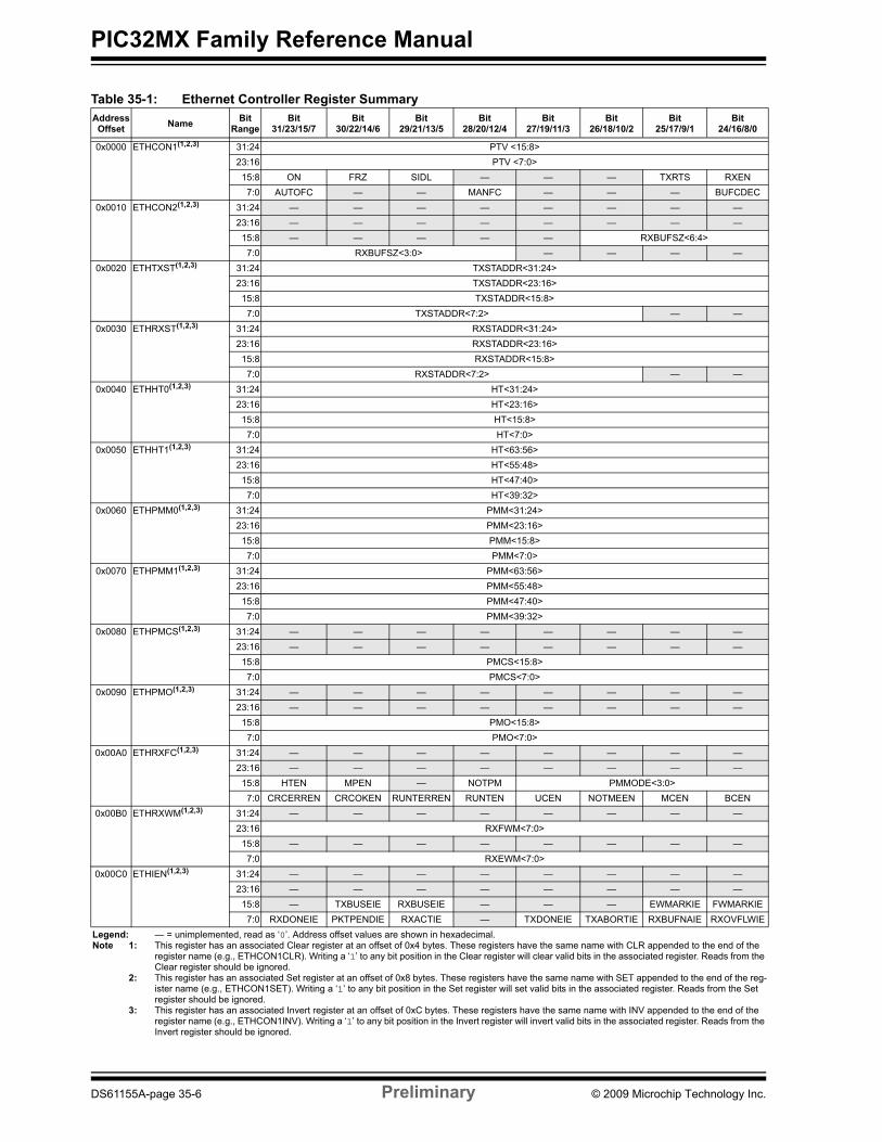
Table 35-1 provides a brief summary of the Ethernet Controller registers. Correspondingregisters appear after the summary, followed by a detailed description of each register.
© 2009 Microchip Technology Inc. Preliminary DS61155A-page 35-5
PIC32MX Family Reference Manual
Table 35-1: Ethernet Controller Register SummaryAddressOffset Name Bit
RangeBit
31/23/15/7Bit
30/22/14/6Bit
29/21/13/5Bit
28/20/12/4Bit
27/19/11/3Bit
26/18/10/2Bit
25/17/9/1Bit
24/16/8/0
0x0000 ETHCON1(1,2,3) 31:24 PTV <15:8>23:16 PTV <7:0>
15:8 ON FRZ SIDL — — — TXRTS RXEN7:0 AUTOFC — — MANFC — — — BUFCDEC
0x0010 ETHCON2(1,2,3) 31:24 — — — — — — — —23:16 — — — — — — — —
15:8 — — — — — RXBUFSZ<6:4>7:0 RXBUFSZ<3:0> — — — —
0x0020 ETHTXST(1,2,3) 31:24 TXSTADDR<31:24>23:16 TXSTADDR<23:16>
15:8 TXSTADDR<15:8>7:0 TXSTADDR<7:2> — —
0x0030 ETHRXST(1,2,3) 31:24 RXSTADDR<31:24>23:16 RXSTADDR<23:16>
15:8 RXSTADDR<15:8>7:0 RXSTADDR<7:2> — —
0x0040 ETHHT0(1,2,3) 31:24 HT<31:24>23:16 HT<23:16>
15:8 HT<15:8>7:0 HT<7:0>
0x0050 ETHHT1(1,2,3) 31:24 HT<63:56>23:16 HT<55:48>
15:8 HT<47:40>7:0 HT<39:32>
0x0060 ETHPMM0(1,2,3) 31:24 PMM<31:24>23:16 PMM<23:16>
15:8 PMM<15:8>7:0 PMM<7:0>
0x0070 ETHPMM1(1,2,3) 31:24 PMM<63:56>23:16 PMM<55:48>
15:8 PMM<47:40>7:0 PMM<39:32>
0x0080 ETHPMCS(1,2,3) 31:24 — — — — — — — —23:16 — — — — — — — —
15:8 PMCS<15:8>7:0 PMCS<7:0>
0x0090 ETHPMO(1,2,3) 31:24 — — — — — — — —23:16 — — — — — — — —
15:8 PMO<15:8>7:0 PMO<7:0>
0x00A0 ETHRXFC(1,2,3) 31:24 — — — — — — — —23:16 — — — — — — — —
15:8 HTEN MPEN — NOTPM PMMODE<3:0>7:0 CRCERREN CRCOKEN RUNTERREN RUNTEN UCEN NOTMEEN MCEN BCEN
0x00B0 ETHRXWM(1,2,3) 31:24 — — — — — — — —23:16 RXFWM<7:0>
15:8 — — — — — — — —7:0 RXEWM<7:0>
0x00C0 ETHIEN(1,2,3) 31:24 — — — — — — — —23:16 — — — — — — — —
15:8 — TXBUSEIE RXBUSEIE — — — EWMARKIE FWMARKIE7:0 RXDONEIE PKTPENDIE RXACTIE — TXDONEIE TXABORTIE RXBUFNAIE RXOVFLWIE
Legend: — = unimplemented, read as ‘0’. Address offset values are shown in hexadecimal.Note 1: This register has an associated Clear register at an offset of 0x4 bytes. These registers have the same name with CLR appended to the end of the
register name (e.g., ETHCON1CLR). Writing a ‘1’ to any bit position in the Clear register will clear valid bits in the associated register. Reads from the Clear register should be ignored.
2: This register has an associated Set register at an offset of 0x8 bytes. These registers have the same name with SET appended to the end of the reg-ister name (e.g., ETHCON1SET). Writing a ‘1’ to any bit position in the Set register will set valid bits in the associated register. Reads from the Set register should be ignored.
3: This register has an associated Invert register at an offset of 0xC bytes. These registers have the same name with INV appended to the end of the register name (e.g., ETHCON1INV). Writing a ‘1’ to any bit position in the Invert register will invert valid bits in the associated register. Reads from the Invert register should be ignored.
DS61155A-page 35-6 Preliminary © 2009 Microchip Technology Inc.

Section 35. Ethernet ControllerEthernet
Controller
35
0x00D0 ETHIRQ(1,2,3) 31:24 — — — — — — — —23:16 — — — — — — — —
15:8 — TXBUSE RXBUSE — — — EWMARK FWMARK7:0 RXDONE PKTPEND RXACT — TXDONE TXABORT RXBUFNA RXOVFLW
0x00E0 ETHSTAT 31:24 — — — — — — — —23:16 BUFCNT<7:0>
15:8 — — — — — — — —7:0 ETHBUSY TXBUSY RXBUSY — — — — —
0x0100 ETHRXOVFLOW(1,2,3) 31:24 — — — — — — — —23:16 — — — — — — — —
15:8 RXOVFLWCNT<15:8>7:0 RXOVFLWCNT<7:0>
0x0110 ETHFRMTXOK(1,2,3) 31:24 — — — — — — — —23:16 — — — — — — — —
15:8 FRMTXOKCNT<15:8>7:0 FRMTXOKCNT<7:0>
0x0120 ETHSCOLFRM(1,2,3) 31:24 — — — — — — — —23:16 — — — — — — — —
15:8 SCOLFRMCNT<15:8>7:0 SCOLFRMCNT<7:0>
0x0130 ETHMCOLFRM(1,2,3) 31:24 — — — — — — — —23:16 — — — — — — — —
15:8 MCOLFRMCNT<15:8>7:0 MCOLFRMCNT<7:0>
0x0140 ETHFRMRXOK(1,2,3) 31:24 — — — — — — — —23:16 — — — — — — — —
15:8 FRMRXOKCNT<15:8>7:0 FRMRXOKCNT<7:0>
0x0150 ETHFCSERR(1,2,3) 31:24 — — — — — — — —23:16 — — — — — — — —
15:8 FCSERRCNT<15:8>7:0 FCSERRCNT<7:0>
0x0160 ETHALGNERR(1,2,3) 31:24 — — — — — — — —23:16 — — — — — — — —
15:8 ALGNERRCNT<15:8>7:0 ALGNERRCNT<7:0>
0x0200 EMACxCFG1(1,2,3) 31:24 — — — — — — — —23:16 — — — — — — — —
15:8 SOFTRESET SIMRESET — — RESETRMCS RESETRFUN RESETTMCS RESETTFUN7:0 — — — LOOPBACK TXPAUSE RXPAUSE PASSALL RXENABLE
0x0210 EMACxCFG2(1,2,3) 31:24 — — — — — — — —23:16 — — — — — — — —
15:8 — EXCESSDFR BPNOBKOFF NOBKOFF — — LONGPRE PUREPRE7:0 AUTOPAD VLANPAD PADENABLE CRCENABLE DELAYCRC HUGEFRM LENGTHCK FULLDPLX
0x0220 EMACxIPGT (1,2,3) 31:24 — — — — — — — —23:16 — — — — — — — —
15:8 — — — — — — — —7:0 — B2BIPKTGP<6:0>
0x0230 EMACxIPGR(1,2,3) 31:24 — — — — — — — —23:16 — — — — — — — —
15:8 — NB2BIPKTGP1<6:0>7:0 — NB2BIPKTGP2<6:0>
Table 35-1: Ethernet Controller Register Summary (Continued)AddressOffset Name Bit
RangeBit
31/23/15/7Bit
30/22/14/6Bit
29/21/13/5Bit
28/20/12/4Bit
27/19/11/3Bit
26/18/10/2Bit
25/17/9/1Bit
24/16/8/0
Legend: — = unimplemented, read as ‘0’. Address offset values are shown in hexadecimal.Note 1: This register has an associated Clear register at an offset of 0x4 bytes. These registers have the same name with CLR appended to the end of the
register name (e.g., ETHCON1CLR). Writing a ‘1’ to any bit position in the Clear register will clear valid bits in the associated register. Reads from the Clear register should be ignored.
2: This register has an associated Set register at an offset of 0x8 bytes. These registers have the same name with SET appended to the end of the reg-ister name (e.g., ETHCON1SET). Writing a ‘1’ to any bit position in the Set register will set valid bits in the associated register. Reads from the Set register should be ignored.
3: This register has an associated Invert register at an offset of 0xC bytes. These registers have the same name with INV appended to the end of the register name (e.g., ETHCON1INV). Writing a ‘1’ to any bit position in the Invert register will invert valid bits in the associated register. Reads from the Invert register should be ignored.
© 2009 Microchip Technology Inc. Preliminary DS61155A-page 35-7

PIC32MX Family Reference Manual
0x0240 EMACxCLRT(1,2,3) 31:24 — — — — — — — —23:16 — — — — — — — —
15:8 — — CWINDOW<5:0>7:0 — — — — RETX<3:0>
0x0250 EMACxMAXF(1,2,3) 31:24 — — — — — — — —23:16 — — — — — — — —
15:8 MACMAXF<15:8>7:0 MACMAXF<7:0>
0x0260 EMACxSUPP(1,2,3) 31:24 — — — — — — — —23:16 — — — — — — — —
15:8 — — — — RESETRMII — — SPEEDRMII7:0 — — — — — — — —
0x0270 EMACxTEST(1,2,3) 31:24 — — — — — — — —23:16 — — — — — — — —
15:8 — — — — — — — —7:0 — — — — — TESTBP TESTPAUSE SHRTQNTA
0x0280 EMACxMCFG(1,2,3) 31:24 — — — — — — — —23:16 — — — — — — — —
15:8 RESETMGMT — — — — — — —7:0 — — CLKSEL<3:0> NOPRE SCANINC
0x0290 EMACxMCMD(1,2,3) 31:24 — — — — — — — —23:16 — — — — — — — —
15:8 — — — — — — — —7:0 — — — — — — SCAN READ
0x02A0 EMACxMADR(1,2,3) 31:24 — — — — — — — —23:16 — — — — — — — —
15:8 — — — PHYADDR<4:0>7:0 — — — REGADDR<4:0>
0x02B0 EMACxMWTD(1,2,3) 31:24 — — — — — — — —23:16 — — — — — — — —
15:8 MWTD<15:8>7:0 MWTD<7:0>
0x02C0 EMACxMRDD(1,2,3) 31:24 — — — — — — — —23:16 — — — — — — — —
15:8 MRDD<15:8>7:0 MRDD<7:0>
0x02D0 EMACxMIND(1,2,3) 31:24 — — — — — — — —23:16 — — — — — — — —
15:8 — — — — — — — —7:0 — — — — LINKFAIL NOTVALID SCAN MIIMBUSY
0x0300 EMACxSA0(1,2,3) 31:24 — — — — — — — —23:16 — — — — — — — —
15:8 STNADDR6<7:0>7:0 STNADDR5<7:0>
0x0310 EMACxSA1(1,2,3) 31:24 — — — — — — — —23:16 — — — — — — — —
15:8 STNADDR4<7:0>7:0 STNADDR3<7:0>
0x0320 EMACxSA2(1,2,3) 31:24 — — — — — — — —23:16 — — — — — — — —
15:8 STNADDR2<7:0>7:0 STNADDR1<7:0>
Table 35-1: Ethernet Controller Register Summary (Continued)AddressOffset Name Bit
RangeBit
31/23/15/7Bit
30/22/14/6Bit
29/21/13/5Bit
28/20/12/4Bit
27/19/11/3Bit
26/18/10/2Bit
25/17/9/1Bit
24/16/8/0
Legend: — = unimplemented, read as ‘0’. Address offset values are shown in hexadecimal.Note 1: This register has an associated Clear register at an offset of 0x4 bytes. These registers have the same name with CLR appended to the end of the
register name (e.g., ETHCON1CLR). Writing a ‘1’ to any bit position in the Clear register will clear valid bits in the associated register. Reads from the Clear register should be ignored.
2: This register has an associated Set register at an offset of 0x8 bytes. These registers have the same name with SET appended to the end of the reg-ister name (e.g., ETHCON1SET). Writing a ‘1’ to any bit position in the Set register will set valid bits in the associated register. Reads from the Set register should be ignored.
3: This register has an associated Invert register at an offset of 0xC bytes. These registers have the same name with INV appended to the end of the register name (e.g., ETHCON1INV). Writing a ‘1’ to any bit position in the Invert register will invert valid bits in the associated register. Reads from the Invert register should be ignored.
DS61155A-page 35-8 Preliminary © 2009 Microchip Technology Inc.

Section 35. Ethernet ControllerEthernet
Controller
35
Register 35-1: ETHCON1: Ethernet Controller Control 1 Register(1,2,3) R/W-0 R/W-0 R/W-0 R/W-0 R/W-0 R/W-0 R/W-0 R/W-0
PTV<15:8>bit 31 bit 24
R/W-0 R/W-0 R/W-0 R/W-0 R/W-0 R/W-0 R/W-0 R/W-0PTV<7:0>
bit 23 bit 16
R/W-0 R/W-0 R/W-0 r-x r-x r-x R/W-0 R/W-0ON FRZ SIDL — — — TXRTS RXEN(4)
bit 15 bit 8
R/W-0 r-x r-x R/W-0 r-x r-x r-x R/W-0AUTOFC — — MANFC — — — BUFCDEC
bit 7 bit 0
Legend:R = Readable bit W = Writable bit P = Programmable bit r = Reserved bitU = Unimplemented bit -n = Bit Value at POR: (‘0’, ‘1’, x = Unknown)
bit 31-16 PTV<15:0>: PAUSE Timer Value bitsPAUSE Timer Value used for Flow Control. This register should only be written when RXEN (ETHCON1<8>) is not set.
These bits are used for Flow Control operations only.bit 15 ON: Ethernet ON bit
1 = Ethernet module is enabled0 = Ethernet module is disabled
bit 14 FRZ: Ethernet Freeze bit1 = Ethernet module is frozen during Debug mode0 = Ethernet module continues to run during Debug mode
bit 13 SIDL: Ethernet Stop in Idle Mode bit1 = Ethernet module transfers are frozen during Idle0 = Ethernet module transfers continue during Idle
bit 12-10 Reserved: Maintain as ‘0’; ignore read
Note 1: This register has an associated Clear register (ETHCON1CLR) at an offset of 0x4 bytes. Writing a ‘1’ toany bit position in the Clear register will clear valid bits in the associated register. Reads from the Clearregister should be ignored.
2: This register has an associated Set register (ETHCON1SET) at an offset of 0x8 bytes. Writing a ‘1’ to anybit position in the Set register will set valid bits in the associated register. Reads from the Set registershould be ignored.
3: This register has an associated Invert register (ETHCON1INV) at an offset of 0xC bytes. Writing a ‘1’ toany bit position in the Invert register will invert valid bits in the associated register. Reads from the Invertregister should be ignored.
4: It is not recommended to clear the RXEN bit and then make changes to any RX related field/register. TheEthernet Controller must be reinitialized (ON cleared to ‘0’), and then the RX changes applied.
© 2009 Microchip Technology Inc. Preliminary DS61155A-page 35-9

PIC32MX Family Reference Manual
bit 9 TXRTS: Transmit Request to Send bit1 = Activate the transmit logic and send the packet(s) defined in the TX EDT0 = Stop transmit (when cleared by software) or transmit done (when cleared by hardware)
After the bit is written with a ‘1’, it will clear to a ‘0’ whenever the transmit logic has finished transmittingthe requested packets in the Ethernet Descriptor Table (EDT). If a ‘0’ is written by the CPU, the transmitlogic finishes the current packet’s transmission and then stops any further.
This bit affects TX operations only.bit 8 RXEN: Receive Enable bit(4)
1 = Enable RX logic, packets are received and stored in the RX buffer as controlled by the filter configuration
0 = Disable RX logic, no packets are received in the RX buffer
This bit affects RX operations only.bit 7 AUTOFC: Automatic Flow Control bit
1 = Automatic flow control enabled0 = Automatic flow control disabled
Setting this bit will enable automatic flow control. If set, the full and empty watermarks are used toautomatically enable and disable the flow control, respectively. When the number of received buffersBUFCNT (ETHSTAT<16:23>) rises to the full watermark, flow control is automatically enabled. Whenthe BUFCNT falls to the empty watermark, flow control is automatically disabled.
This bit is used for flow control operations only and affects both TX and RX operations.bit 6-5 Reserved: Maintain as ‘0’; ignore readbit 4 MANFC: Manual Flow Control bit
1 = Manual Flow Control enabled0 = Manual Flow Control disabled
Setting this bit will enable manual flow control. If set, the flow control logic will send a PAUSE frameusing the PAUSE timer value in the PTV register. It will then resend a PAUSE frame every 128 *PTV<15:0>/2 TX clock cycles until the bit is cleared.
Note that for 10 Mbps operation, TX clock runs at 2.5 MHz. For 100 Mbps operation, TX clock runs at25 MHz.
When this bit is cleared, the Flow Control logic will automatically send a PAUSE frame with a 0x0000PAUSE timer value to disable flow control.
This bit is used for flow control operations only and affects both TX and RX operations.bit 3-1 Reserved: Maintain as ‘0’; ignore readbit 0 BUFCDEC: Descriptor Buffer Count Decrement bit
The BUFCDEC bit is a write-1 bit that reads out ‘0’. When written with ‘1’, BUFCNT, the DescriptorBuffer Counter, will decrement by one. If the BUFCNT counter is incremented by the RX logic at thesame time that this bit is written, the BUFCNT value will remain unchanged. Writing ‘0’ will have noeffect.
This bit is used for RX operations only.
Register 35-1: ETHCON1: Ethernet Controller Control 1 Register(1,2,3) (Continued)
Note 1: This register has an associated Clear register (ETHCON1CLR) at an offset of 0x4 bytes. Writing a ‘1’ toany bit position in the Clear register will clear valid bits in the associated register. Reads from the Clearregister should be ignored.
2: This register has an associated Set register (ETHCON1SET) at an offset of 0x8 bytes. Writing a ‘1’ to anybit position in the Set register will set valid bits in the associated register. Reads from the Set registershould be ignored.
3: This register has an associated Invert register (ETHCON1INV) at an offset of 0xC bytes. Writing a ‘1’ toany bit position in the Invert register will invert valid bits in the associated register. Reads from the Invertregister should be ignored.
4: It is not recommended to clear the RXEN bit and then make changes to any RX related field/register. TheEthernet Controller must be reinitialized (ON cleared to ‘0’), and then the RX changes applied.
DS61155A-page 35-10 Preliminary © 2009 Microchip Technology Inc.
Section 35. Ethernet ControllerEthernet
Controller
35
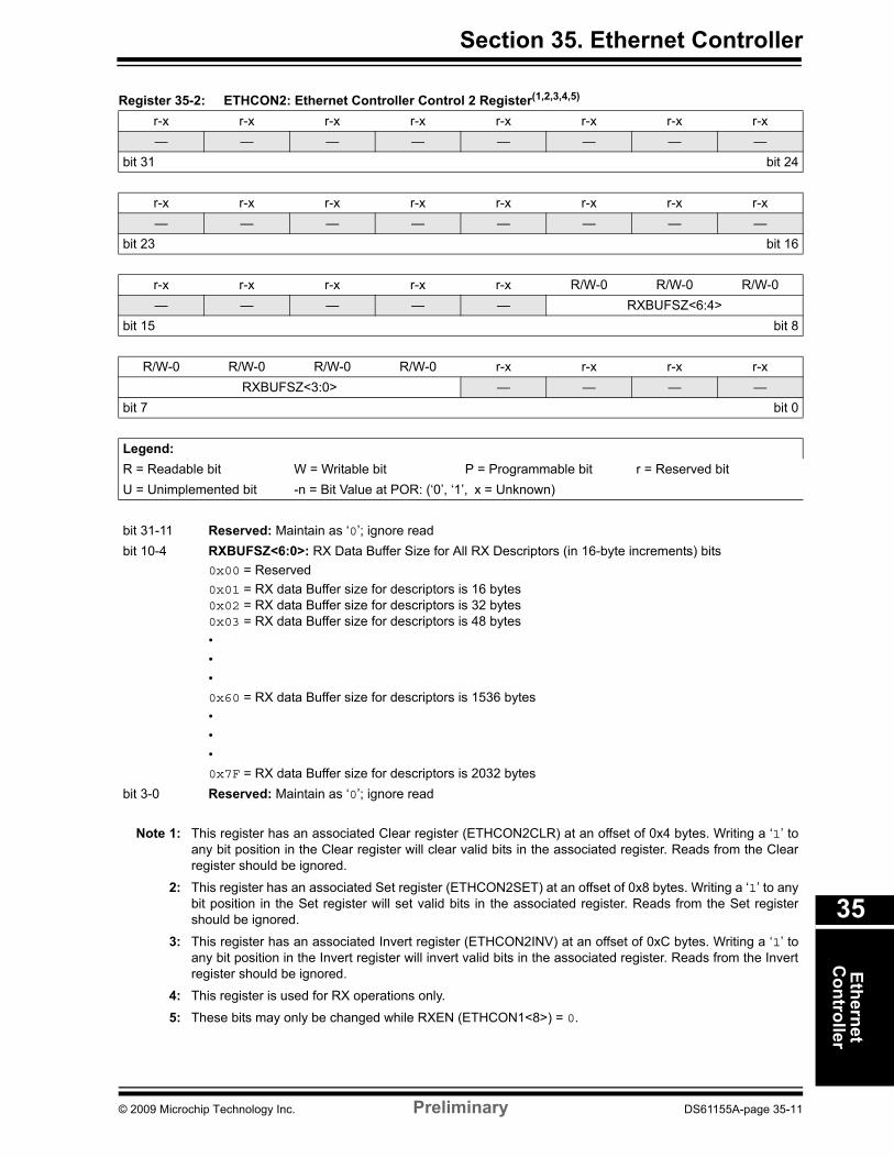
Register 35-2: ETHCON2: Ethernet Controller Control 2 Register(1,2,3,4,5)
r-x r-x r-x r-x r-x r-x r-x r-x— — — — — — — —
bit 31 bit 24
r-x r-x r-x r-x r-x r-x r-x r-x— — — — — — — —
bit 23 bit 16
r-x r-x r-x r-x r-x R/W-0 R/W-0 R/W-0— — — — — RXBUFSZ<6:4>
bit 15 bit 8
R/W-0 R/W-0 R/W-0 R/W-0 r-x r-x r-x r-xRXBUFSZ<3:0> — — — —
bit 7 bit 0
Legend:R = Readable bit W = Writable bit P = Programmable bit r = Reserved bitU = Unimplemented bit -n = Bit Value at POR: (‘0’, ‘1’, x = Unknown)
bit 31-11 Reserved: Maintain as ‘0’; ignore readbit 10-4 RXBUFSZ<6:0>: RX Data Buffer Size for All RX Descriptors (in 16-byte increments) bits
0x00 = Reserved0x01 = RX data Buffer size for descriptors is 16 bytes0x02 = RX data Buffer size for descriptors is 32 bytes0x03 = RX data Buffer size for descriptors is 48 bytes•••0x60 = RX data Buffer size for descriptors is 1536 bytes•••0x7F = RX data Buffer size for descriptors is 2032 bytes
bit 3-0 Reserved: Maintain as ‘0’; ignore read
Note 1: This register has an associated Clear register (ETHCON2CLR) at an offset of 0x4 bytes. Writing a ‘1’ toany bit position in the Clear register will clear valid bits in the associated register. Reads from the Clearregister should be ignored.
2: This register has an associated Set register (ETHCON2SET) at an offset of 0x8 bytes. Writing a ‘1’ to anybit position in the Set register will set valid bits in the associated register. Reads from the Set registershould be ignored.
3: This register has an associated Invert register (ETHCON2INV) at an offset of 0xC bytes. Writing a ‘1’ toany bit position in the Invert register will invert valid bits in the associated register. Reads from the Invertregister should be ignored.
4: This register is used for RX operations only.
5: These bits may only be changed while RXEN (ETHCON1<8>) = 0.
© 2009 Microchip Technology Inc. Preliminary DS61155A-page 35-11

PIC32MX Family Reference Manual
Register 35-3: ETHTXST: Ethernet Controller TX Packet Descriptor Start Address Register(1,2,3,4,5)
R/W-0 R/W-0 R/W-0 R/W-0 R/W-0 R/W-0 R/W-0 R/W-0TXSTADDR<31:24>
bit 31 bit 24
R/W-0 R/W-0 R/W-0 R/W-0 R/W-0 R/W-0 R/W-0 R/W-0TXSTADDR<23:16>
bit 23 bit 16
R/W-0 R/W-0 R/W-0 R/W-0 R/W-0 R/W-0 R/W-0 R/W-0TXSTADDR<15:8>
bit 15 bit 8
R/W-0 R/W-0 R/W-0 R/W-0 R/W-0 R/W-0 r-0 r-0TXSTADDR<7:2> — —
bit 7 bit 0
Legend:R = Readable bit W = Writable bit P = Programmable bit r = Reserved bitU = Unimplemented bit -n = Bit Value at POR: (‘0’, ‘1’, x = Unknown)
bit 31-2 TXSTADDR<31:2>: Starting Address of First Transmit Descriptor bitsThis register should not be written while any transmit, receive or DMA operations are in progress.This address must be 4-byte aligned (i.e., bits 1-0 must be ‘00’).
bit 1-0 Reserved: Maintain as ‘0’; ignore read
Note 1: This register has an associated Clear register (ETHTXSTCLR) at an offset of 0x4 bytes. Writing a ‘1’ toany bit position in the Clear register will clear valid bits in the associated register. Reads from the Clearregister should be ignored.
2: This register has an associated Set register (ETHTXSTSET) at an offset of 0x8 bytes. Writing a ‘1’ to anybit position in the Set register will set valid bits in the associated register. Reads from the Set registershould be ignored.
3: This register has an associated Invert register (ETHTXSTINV) at an offset of 0xC bytes. Writing a ‘1’ toany bit position in the Invert register will invert valid bits in the associated register. Reads from the Invertregister should be ignored.
4: This register is used for TX operations only.
5: This register will be updated by hardware with the last descriptor used by the last successfully transmittedpacket.
DS61155A-page 35-12 Preliminary © 2009 Microchip Technology Inc.

Section 35. Ethernet ControllerEthernet
Controller
35
Register 35-4: ETHRXST: Ethernet Controller RX Packet Descriptor Start Address Register(1,2,3,4,5)
R/W-0 R/W-0 R/W-0 R/W-0 R/W-0 R/W-0 R/W-0 R/W-0RXSTADDR<31:24>
bit 31 bit 24
R/W-0 R/W-0 R/W-0 R/W-0 R/W-0 R/W-0 R/W-0 R/W-0RXSTADDR<23:16>
bit 23 bit 16
R/W-0 R/W-0 R/W-0 R/W-0 R/W-0 R/W-0 R/W-0 R/W-0RXSTADDR<15:8>
bit 15 bit 8
R/W-0 R/W-0 R/W-0 R/W-0 R/W-0 R/W-0 r-0 r-0RXSTADDR<7:2> — —
bit 7 bit 0
Legend:R = Readable bit W = Writable bit P = Programmable bit r = Reserved bitU = Unimplemented bit -n = Bit Value at POR: (‘0’, ‘1’, x = Unknown)
bit 31-2 RXSTADDR<31:2>: Starting Address of First Receive Descriptor bitsThis register should not be written while any transmit, receive or DMA operations are in progress.This address must be 4-byte aligned (i.e., bits 1-0 must be ‘00’).
bit 1-0 Reserved: Maintain as ‘0’; ignore read
Note 1: This register has an associated Clear register (ETHRXSTCLR) at an offset of 0x4 bytes. Writing a ‘1’ toany bit position in the Clear register will clear valid bits in the associated register. Reads from the Clearregister should be ignored.
2: This register has an associated Set register (ETHRXSTSET) at an offset of 0x8 bytes. Writing a ‘1’ to anybit position in the Set register will set valid bits in the associated register. Reads from the Set registershould be ignored.
3: This register has an associated Invert register (ETHRXSTINV) at an offset of 0xC bytes. Writing a ‘1’ toany bit position in the Invert register will invert valid bits in the associated register. Reads from the Invertregister should be ignored.
4: This register is used for RX operations only.
5: This register will be updated by hardware with the last descriptor used by the last successfully transmittedpacket.
© 2009 Microchip Technology Inc. Preliminary DS61155A-page 35-13

PIC32MX Family Reference Manual
Register 35-5: ETHHT0: Ethernet Controller Hash Table 0 Register(1,2,3,4,5)
R/W-0 R/W-0 R/W-0 R/W-0 R/W-0 R/W-0 R/W-0 R/W-0HT<31:24>
bit 31 bit 24
R/W-0 R/W-0 R/W-0 R/W-0 R/W-0 R/W-0 R/W-0 R/W-0HT<23:16>
bit 23 bit 16
R/W-0 R/W-0 R/W-0 R/W-0 R/W-0 R/W-0 R/W-0 R/W-0HT<15:8>
bit 15 bit 8
R/W-0 R/W-0 R/W-0 R/W-0 R/W-0 R/W-0 R/W-0 R/W-0HT<7:0>
bit 7 bit 0
Legend:R = Readable bit W = Writable bit P = Programmable bit r = Reserved bitU = Unimplemented bit -n = Bit Value at POR: (‘0’, ‘1’, x = Unknown)
bit 31-0 HT<31:0>: Hash Table Bytes 0-3 bits
Note 1: This register has an associated Clear register (ETHTXSTCLR) at an offset of 0x4 bytes. Writing a ‘1’ toany bit position in the Clear register will clear valid bits in the associated register. Reads from the Clearregister should be ignored.
2: This register has an associated Set register (ETHTXSTSET) at an offset of 0x8 bytes. Writing a ‘1’ to anybit position in the Set register will set valid bits in the associated register. Reads from the Set registershould be ignored.
3: This register has an associated Invert register (ETHTXSTINV) at an offset of 0xC bytes. Writing a ‘1’ toany bit position in the Invert register will invert valid bits in the associated register. Reads from the Invertregister should be ignored.
4: This register is used for RX operations only.
5: These bits may only be changed while RXEN (ETHCON1<8>) = 0 or HTEN (ETHRXFC<15>) = 0.
DS61155A-page 35-14 Preliminary © 2009 Microchip Technology Inc.

Section 35. Ethernet ControllerEthernet
Controller
35
Register 35-6: ETHHT1: Ethernet Controller Hash Table 1 Register(1,2,3,4,5)
R/W-0 R/W-0 R/W-0 R/W-0 R/W-0 R/W-0 R/W-0 R/W-0HT<63:56>
bit 31 bit 24
R/W-0 R/W-0 R/W-0 R/W-0 R/W-0 R/W-0 R/W-0 R/W-0HT<55:48>
bit 23 bit 16
R/W-0 R/W-0 R/W-0 R/W-0 R/W-0 R/W-0 R/W-0 R/W-0HT<47:40>
bit 15 bit 8
R/W-0 R/W-0 R/W-0 R/W-0 R/W-0 R/W-0 R/W-0 R/W-0HT<39:32>
bit 7 bit 0
Legend:R = Readable bit W = Writable bit P = Programmable bit r = Reserved bitU = Unimplemented bit -n = Bit Value at POR: (‘0’, ‘1’, x = Unknown)
bit 31-0 HT<63:32>: Hash Table Bytes 4-7 bits
Note 1: This register has an associated Clear register (ETHHT1CLR) at an offset of 0x4 bytes. Writing a ‘1’ to anybit position in the Clear register will clear valid bits in the associated register. Reads from the Clear registershould be ignored.
2: This register has an associated Set register (ETHHT1SET) at an offset of 0x8 bytes. Writing a ‘1’ to anybit position in the Set register will set valid bits in the associated register. Reads from the Set registershould be ignored.
3: This register has an associated Invert register (ETHHT1INV) at an offset of 0xC bytes. Writing a ‘1’ to anybit position in the Invert register will invert valid bits in the associated register. Reads from the Invert reg-ister should be ignored.
4: This register is used for RX operations only.
5: These bits may only be changed while RXEN (ETHCON1<8>) = 0 or HTEN (ETHRXFC<15>) = 0.
© 2009 Microchip Technology Inc. Preliminary DS61155A-page 35-15

PIC32MX Family Reference Manual
Register 35-7: ETHPMM0: Ethernet Controller Pattern Match Mask 0 Register(1,2,3,4,5)
R/W-0 R/W-0 R/W-0 R/W-0 R/W-0 R/W-0 R/W-0 R/W-0PMM<31:24>
bit 31 bit 24
R/W-0 R/W-0 R/W-0 R/W-0 R/W-0 R/W-0 R/W-0 R/W-0PMM<23:16>
bit 23 bit 16
R/W-0 R/W-0 R/W-0 R/W-0 R/W-0 R/W-0 R/W-0 R/W-0PMM<15:8>
bit 15 bit 8
R/W-0 R/W-0 R/W-0 R/W-0 R/W-0 R/W-0 R/W-0 R/W-0PMM<7:0>
bit 7 bit 0
Legend:R = Readable bit W = Writable bit P = Programmable bit r = Reserved bitU = Unimplemented bit -n = Bit Value at POR: (‘0’, ‘1’, x = Unknown)
bit 31-24 PMM<31:24>: Pattern Match Mask 3 bitsbit 23-16 PMM<23:16>: Pattern Match Mask 2 bitsbit 15-8 PMM<15:8>: Pattern Match Mask 1 bitsbit 7-0 PMM<7:0>: Pattern Match Mask 0 bits
Note 1: This register has an associated Clear register (ETHPMM0CLR) at an offset of 0x4 bytes. Writing a ‘1’ toany bit position in the Clear register will clear valid bits in the associated register. Reads from the Clearregister should be ignored.
2: This register has an associated Set register (ETHPMM0SET) at an offset of 0x8 bytes. Writing a ‘1’ to anybit position in the Set register will set valid bits in the associated register. Reads from the Set registershould be ignored.
3: This register has an associated Invert register (ETHPMM0INV) at an offset of 0xC bytes. Writing a ‘1’ toany bit position in the Invert register will invert valid bits in the associated register. Reads from the Invertregister should be ignored.
4: This register is used for RX operations only.
5: These bits may only be changed while RXEN (ETHCON1<8>) = 0 or PMMODE (ETHRXFC<11:8>) = 0.
DS61155A-page 35-16 Preliminary © 2009 Microchip Technology Inc.

Section 35. Ethernet ControllerEthernet
Controller
35
Register 35-8: ETHPMM1: Ethernet Controller Pattern Match Mask 1 Register(1,2,3,4,5)
R/W-0 R/W-0 R/W-0 R/W-0 R/W-0 R/W-0 R/W-0 R/W-0PMM<63:56>
bit 31 bit 24
R/W-0 R/W-0 R/W-0 R/W-0 R/W-0 R/W-0 R/W-0 R/W-0PMM<55:48>
bit 23 bit 16
R/W-0 R/W-0 R/W-0 R/W-0 R/W-0 R/W-0 R/W-0 R/W-0PMM<47:40>
bit 15 bit 8
R/W-0 R/W-0 R/W-0 R/W-0 R/W-0 R/W-0 R/W-0 R/W-0PMM<39:32>
bit 7 bit 0
Legend:R = Readable bit W = Writable bit P = Programmable bit r = Reserved bitU = Unimplemented bit -n = Bit Value at POR: (‘0’, ‘1’, x = Unknown)
bit 31-24 PMM<63:56>: Pattern Match Mask 7 bitsbit 23-16 PMM<55:48>: Pattern Match Mask 6 bitsbit 15-8 PMM<47:40>: Pattern Match Mask 5 bitsbit 7-0 PMM<39:32>: Pattern Match Mask 4 bits
Note 1: This register has an associated Clear register (ETHPMM1CLR) at an offset of 0x4 bytes. Writing a ‘1’ toany bit position in the Clear register will clear valid bits in the associated register. Reads from the Clearregister should be ignored.
2: This register has an associated Set register (ETHPMM1SET) at an offset of 0x8 bytes. Writing a ‘1’ to anybit position in the Set register will set valid bits in the associated register. Reads from the Set registershould be ignored.
3: This register has an associated Invert register (ETHPMM1INV) at an offset of 0xC bytes. Writing a ‘1’ toany bit position in the Invert register will invert valid bits in the associated register. Reads from the Invertregister should be ignored.
4: This register is used for RX operations only.
5: These bits may only be changed while RXEN (ETHCON1<8>) = 0 or PMMODE (ETHRXFC<11:8>) = 0.
© 2009 Microchip Technology Inc. Preliminary DS61155A-page 35-17

PIC32MX Family Reference Manual
Register 35-9: ETHPMCS: Ethernet Controller Pattern Match Checksum Register(1,2,3,4,5)
r-x r-x r-x r-x r-x r-x r-x r-x— — — — — — — —
bit 31 bit 24
r-x r-x r-x r-x r-x r-x r-x r-x— — — — — — — —
bit 23 bit 16
R/W-0 R/W-0 R/W-0 R/W-0 R/W-0 R/W-0 R/W-0 R/W-0PMCS<15:8>
bit 15 bit 8
R/W-0 R/W-0 R/W-0 R/W-0 R/W-0 R/W-0 R/W-0 R/W-0PMCS<7:0>
bit 7 bit 0
Legend:R = Readable bit W = Writable bit P = Programmable bit r = Reserved bitU = Unimplemented bit -n = Bit Value at POR: (‘0’, ‘1’, x = Unknown)
bit 31-16 Reserved: Maintain as ‘0’; ignore readbit 15-8 PMCS<15:8>: Pattern Match Checksum 1 bitsbit 7-0 PMCS<7:0>: Pattern Match Checksum 0 bits
Note 1: This register has an associated Clear register (ETHPMCSCLR) at an offset of 0x4 bytes. Writing a ‘1’ toany bit position in the Clear register will clear valid bits in the associated register. Reads from the Clearregister should be ignored.
2: This register has an associated Set register (ETHPMCSSET) at an offset of 0x8 bytes. Writing a ‘1’ to anybit position in the Set register will set valid bits in the associated register. Reads from the Set registershould be ignored.
3: This register has an associated Invert register (ETHPMCSINV) at an offset of 0xC bytes. Writing a ‘1’ toany bit position in the Invert register will invert valid bits in the associated register. Reads from the Invertregister should be ignored.
4: This register is used for RX operations only.
5: These bits may only be changed while RXEN (ETHCON1<8>) = 0 or PMMODE (ETHRXFC<11:8>) = 0.
DS61155A-page 35-18 Preliminary © 2009 Microchip Technology Inc.
Section 35. Ethernet ControllerEthernet
Controller
35
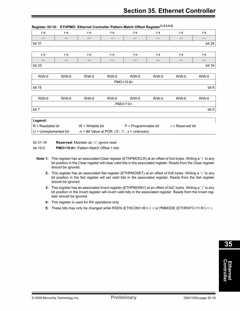
Register 35-10: ETHPMO: Ethernet Controller Pattern Match Offset Register(1,2,3,4,5)
r-x r-x r-x r-x r-x r-x r-x r-x— — — — — — — —
bit 31 bit 24
r-x r-x r-x r-x r-x r-x r-x r-x— — — — — — — —
bit 23 bit 16
R/W-0 R/W-0 R/W-0 R/W-0 R/W-0 R/W-0 R/W-0 R/W-0PMO<15:8>
bit 15 bit 8
R/W-0 R/W-0 R/W-0 R/W-0 R/W-0 R/W-0 R/W-0 R/W-0PMO<7:0>
bit 7 bit 0
Legend:R = Readable bit W = Writable bit P = Programmable bit r = Reserved bitU = Unimplemented bit -n = Bit Value at POR: (‘0’, ‘1’, x = Unknown)
bit 31-16 Reserved: Maintain as ‘0’; ignore readbit 15-0 PMO<15:0>: Pattern Match Offset 1 bits
Note 1: This register has an associated Clear register (ETHPMOCLR) at an offset of 0x4 bytes. Writing a ‘1’ to anybit position in the Clear register will clear valid bits in the associated register. Reads from the Clear registershould be ignored.
2: This register has an associated Set register (ETHPMOSET) at an offset of 0x8 bytes. Writing a ‘1’ to anybit position in the Set register will set valid bits in the associated register. Reads from the Set registershould be ignored.
3: This register has an associated Invert register (ETHPMOINV) at an offset of 0xC bytes. Writing a ‘1’ to anybit position in the Invert register will invert valid bits in the associated register. Reads from the Invert reg-ister should be ignored.
4: This register is used for RX operations only.
5: These bits may only be changed while RXEN (ETHCON1<8>) = 0 or PMMODE (ETHRXFC<11:8>) = 0.
© 2009 Microchip Technology Inc. Preliminary DS61155A-page 35-19
PIC32MX Family Reference Manual
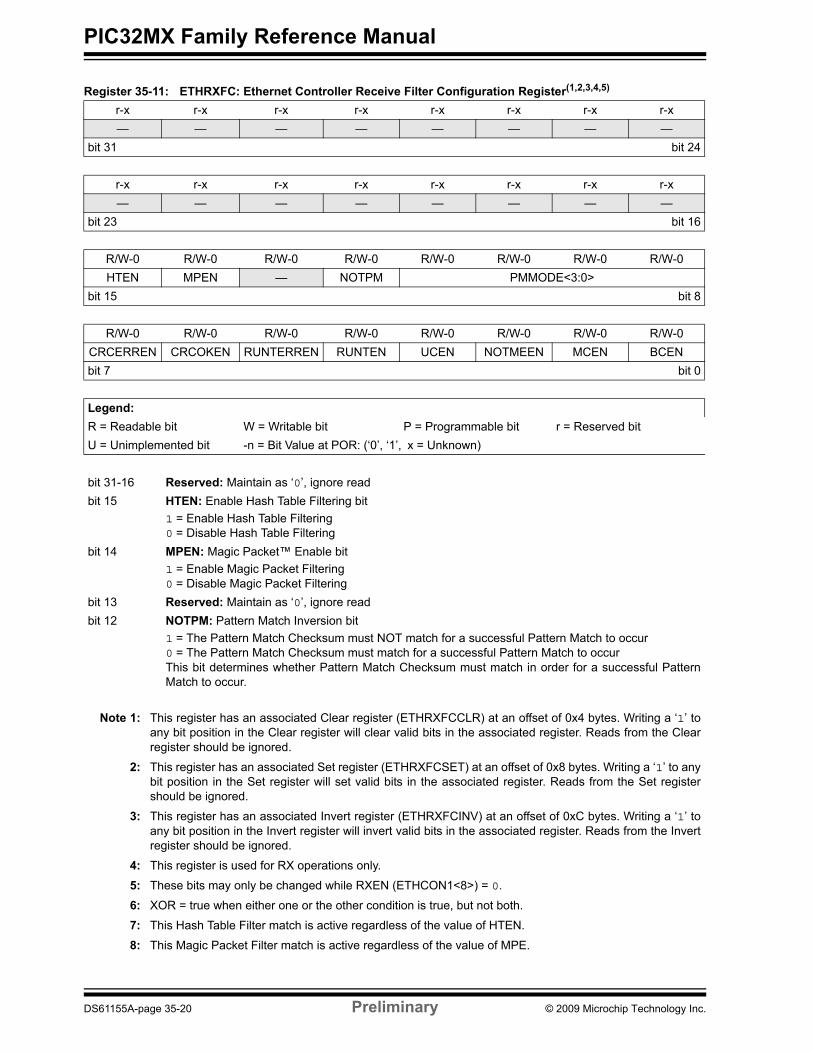
Register 35-11: ETHRXFC: Ethernet Controller Receive Filter Configuration Register(1,2,3,4,5)
r-x r-x r-x r-x r-x r-x r-x r-x— — — — — — — —
bit 31 bit 24
r-x r-x r-x r-x r-x r-x r-x r-x— — — — — — — —
bit 23 bit 16
R/W-0 R/W-0 R/W-0 R/W-0 R/W-0 R/W-0 R/W-0 R/W-0HTEN MPEN — NOTPM PMMODE<3:0>
bit 15 bit 8
R/W-0 R/W-0 R/W-0 R/W-0 R/W-0 R/W-0 R/W-0 R/W-0CRCERREN CRCOKEN RUNTERREN RUNTEN UCEN NOTMEEN MCEN BCENbit 7 bit 0
Legend:R = Readable bit W = Writable bit P = Programmable bit r = Reserved bitU = Unimplemented bit -n = Bit Value at POR: (‘0’, ‘1’, x = Unknown)
bit 31-16 Reserved: Maintain as ‘0’, ignore readbit 15 HTEN: Enable Hash Table Filtering bit
1 = Enable Hash Table Filtering0 = Disable Hash Table Filtering
bit 14 MPEN: Magic Packet™ Enable bit1 = Enable Magic Packet Filtering0 = Disable Magic Packet Filtering
bit 13 Reserved: Maintain as ‘0’, ignore readbit 12 NOTPM: Pattern Match Inversion bit
1 = The Pattern Match Checksum must NOT match for a successful Pattern Match to occur0 = The Pattern Match Checksum must match for a successful Pattern Match to occurThis bit determines whether Pattern Match Checksum must match in order for a successful PatternMatch to occur.
Note 1: This register has an associated Clear register (ETHRXFCCLR) at an offset of 0x4 bytes. Writing a ‘1’ toany bit position in the Clear register will clear valid bits in the associated register. Reads from the Clearregister should be ignored.
2: This register has an associated Set register (ETHRXFCSET) at an offset of 0x8 bytes. Writing a ‘1’ to anybit position in the Set register will set valid bits in the associated register. Reads from the Set registershould be ignored.
3: This register has an associated Invert register (ETHRXFCINV) at an offset of 0xC bytes. Writing a ‘1’ toany bit position in the Invert register will invert valid bits in the associated register. Reads from the Invertregister should be ignored.
4: This register is used for RX operations only.
5: These bits may only be changed while RXEN (ETHCON1<8>) = 0.
6: XOR = true when either one or the other condition is true, but not both.
7: This Hash Table Filter match is active regardless of the value of HTEN.
8: This Magic Packet Filter match is active regardless of the value of MPE.
DS61155A-page 35-20 Preliminary © 2009 Microchip Technology Inc.

Section 35. Ethernet ControllerEthernet
Controller
35
bit 11-8 PMMODE<3:0>: Pattern Match Mode bits0000 = Pattern Match is disabled; pattern match is always unsuccessful0001 = Pattern match is successful if (NOTPM = 1 XOR Pattern Match Checksum matches)(6)
0010 = Pattern match is successful if (NOTPM = 1 XOR Pattern Match Checksum matches) AND(Destination Address = Station Address)(6)
0011 = Pattern match is successful if (NOTPM = 1 XOR Pattern Match Checksum matches) AND(Destination Address = Station Address)(6)
0100 = Pattern match is successful if (NOTPM = 1 XOR Pattern Match Checksum matches) AND(Destination Address = Unicast Address)(6)
0101 = Pattern match is successful if (NOTPM = 1 XOR Pattern Match Checksum matches) AND(Destination Address = Unicast Address)(6)
0110 = Pattern match is successful if (NOTPM = 1 XOR Pattern Match Checksum matches) AND(Destination Address = Broadcast Address)(6)
0111 = Pattern match is successful if (NOTPM = 1 XOR Pattern Match Checksum matches) AND(Destination Address = Broadcast Address)(6)
1000 = Pattern match is successful if (NOTPM = 1 XOR Pattern Match Checksum matches) AND(Hash Table Filter match)(6,7)
1001 = Pattern match is successful if (NOTPM = 1 XOR Pattern Match Checksum matches) AND(Packet = Magic Packet)(6,8)
bit 7 CRCERREN: CRC Error Collection Enable bit1 = The received packet CRC must be invalid for the packet to be accepted0 = Disable CRC Error Collection filteringThis bit allows the user to collect all packets that have an invalid CRC.
bit 6 CRCOKEN: CRC OK Enable bit1 = The received packet CRC must be valid for the packet to be accepted0 = Disable CRC filteringThis bit allows the user to reject all packets that have an invalid CRC.
bit 5 RUNTERREN: Runt Error Collection Enable bit1 = The received packet must be a runt packet for the packet to be accepted0 = Disable Runt Error Collection filtering
This bit allows the user to collect all packets that are runt packets. For this filter, a runt packet is definedas any packet with a size of less than 64 bytes (when CRCOKEN = 0) or any packet with a size of lessthan 64 bytes that has a valid CRC (when CRCOKEN = 1).
bit 4 RUNTEN: Runt Enable bit1 = The received packet must NOT be a runt packet for the packet to be accepted0 = Disable Runt filtering
This bit allows the user to reject all runt packets. For this filter, a runt packet is defined as any packetwith a size of less than 64 bytes.
Register 35-11: ETHRXFC: Ethernet Controller Receive Filter Configuration Register(1,2,3,4,5) (Continued)
Note 1: This register has an associated Clear register (ETHRXFCCLR) at an offset of 0x4 bytes. Writing a ‘1’ toany bit position in the Clear register will clear valid bits in the associated register. Reads from the Clearregister should be ignored.
2: This register has an associated Set register (ETHRXFCSET) at an offset of 0x8 bytes. Writing a ‘1’ to anybit position in the Set register will set valid bits in the associated register. Reads from the Set registershould be ignored.
3: This register has an associated Invert register (ETHRXFCINV) at an offset of 0xC bytes. Writing a ‘1’ toany bit position in the Invert register will invert valid bits in the associated register. Reads from the Invertregister should be ignored.
4: This register is used for RX operations only.
5: These bits may only be changed while RXEN (ETHCON1<8>) = 0.
6: XOR = true when either one or the other condition is true, but not both.
7: This Hash Table Filter match is active regardless of the value of HTEN.
8: This Magic Packet Filter match is active regardless of the value of MPE.
© 2009 Microchip Technology Inc. Preliminary DS61155A-page 35-21
PIC32MX Family Reference Manual
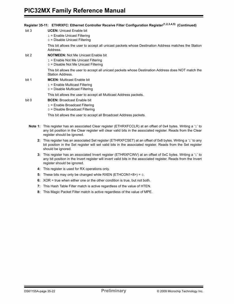
bit 3 UCEN: Unicast Enable bit1 = Enable Unicast Filtering0 = Disable Unicast Filtering
This bit allows the user to accept all unicast packets whose Destination Address matches the StationAddress.
bit 2 NOTMEEN: Not Me Unicast Enable bit1 = Enable Not Me Unicast Filtering0 = Disable Not Me Unicast Filtering
This bit allows the user to accept all unicast packets whose Destination Address does NOT match theStation Address.
bit 1 MCEN: Multicast Enable bit1 = Enable Multicast Filtering0 = Disable Multicast Filtering
This bit allows the user to accept all Multicast Address packets.bit 0 BCEN: Broadcast Enable bit
1 = Enable Broadcast Filtering0 = Disable Broadcast Filtering
This bit allows the user to accept all Broadcast Address packets.
Register 35-11: ETHRXFC: Ethernet Controller Receive Filter Configuration Register(1,2,3,4,5) (Continued)
Note 1: This register has an associated Clear register (ETHRXFCCLR) at an offset of 0x4 bytes. Writing a ‘1’ toany bit position in the Clear register will clear valid bits in the associated register. Reads from the Clearregister should be ignored.
2: This register has an associated Set register (ETHRXFCSET) at an offset of 0x8 bytes. Writing a ‘1’ to anybit position in the Set register will set valid bits in the associated register. Reads from the Set registershould be ignored.
3: This register has an associated Invert register (ETHRXFCINV) at an offset of 0xC bytes. Writing a ‘1’ toany bit position in the Invert register will invert valid bits in the associated register. Reads from the Invertregister should be ignored.
4: This register is used for RX operations only.
5: These bits may only be changed while RXEN (ETHCON1<8>) = 0.
6: XOR = true when either one or the other condition is true, but not both.
7: This Hash Table Filter match is active regardless of the value of HTEN.
8: This Magic Packet Filter match is active regardless of the value of MPE.
DS61155A-page 35-22 Preliminary © 2009 Microchip Technology Inc.
Section 35. Ethernet ControllerEthernet
Controller
35
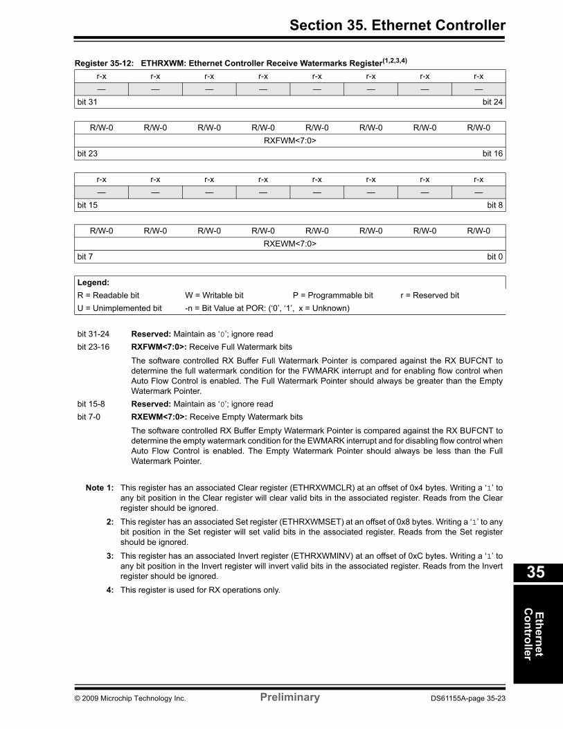
Register 35-12: ETHRXWM: Ethernet Controller Receive Watermarks Register(1,2,3,4)
r-x r-x r-x r-x r-x r-x r-x r-x— — — — — — — —
bit 31 bit 24
R/W-0 R/W-0 R/W-0 R/W-0 R/W-0 R/W-0 R/W-0 R/W-0RXFWM<7:0>
bit 23 bit 16
r-x r-x r-x r-x r-x r-x r-x r-x— — — — — — — —
bit 15 bit 8
R/W-0 R/W-0 R/W-0 R/W-0 R/W-0 R/W-0 R/W-0 R/W-0RXEWM<7:0>
bit 7 bit 0
Legend:R = Readable bit W = Writable bit P = Programmable bit r = Reserved bitU = Unimplemented bit -n = Bit Value at POR: (‘0’, ‘1’, x = Unknown)
bit 31-24 Reserved: Maintain as ‘0’; ignore readbit 23-16 RXFWM<7:0>: Receive Full Watermark bits
The software controlled RX Buffer Full Watermark Pointer is compared against the RX BUFCNT todetermine the full watermark condition for the FWMARK interrupt and for enabling flow control whenAuto Flow Control is enabled. The Full Watermark Pointer should always be greater than the EmptyWatermark Pointer.
bit 15-8 Reserved: Maintain as ‘0’; ignore readbit 7-0 RXEWM<7:0>: Receive Empty Watermark bits
The software controlled RX Buffer Empty Watermark Pointer is compared against the RX BUFCNT todetermine the empty watermark condition for the EWMARK interrupt and for disabling flow control whenAuto Flow Control is enabled. The Empty Watermark Pointer should always be less than the FullWatermark Pointer.
Note 1: This register has an associated Clear register (ETHRXWMCLR) at an offset of 0x4 bytes. Writing a ‘1’ toany bit position in the Clear register will clear valid bits in the associated register. Reads from the Clearregister should be ignored.
2: This register has an associated Set register (ETHRXWMSET) at an offset of 0x8 bytes. Writing a ‘1’ to anybit position in the Set register will set valid bits in the associated register. Reads from the Set registershould be ignored.
3: This register has an associated Invert register (ETHRXWMINV) at an offset of 0xC bytes. Writing a ‘1’ toany bit position in the Invert register will invert valid bits in the associated register. Reads from the Invertregister should be ignored.
4: This register is used for RX operations only.
© 2009 Microchip Technology Inc. Preliminary DS61155A-page 35-23

PIC32MX Family Reference Manual
Register 35-13: ETHIEN: Ethernet Controller Interrupt Enable Register(1,2,3,4,5)
r-x r-x r-x r-x r-x r-x r-x r-x— — — — — — — —
bit 31 bit 24
r-x r-x r-x r-x r-x r-x r-x r-x— — — — — — — —
bit 23 bit 16
r-x R/W-0 R/W-0 r-x r-x r-x R/W-0 R/W-0— TXBUSEIE(4) RXBUSEIE(5) — — — EWMARKIE(5) FWMARKIE(5)
bit 15 bit 8
R/W-0 R/W-0 R/W-0 r-x R/W-0 R/W-0 R/W-0 R/W-0RXDONEIE(5) PKTPENDIE(5) RXACTIE(5) — TXDONEIE(4) TXABORTIE(4) RXBUFNAIE(5) RXOVFLWIE(5)
bit 7 bit 0
Legend:R = Readable bit W = Writable bit P = Programmable bit r = Reserved bitU = Unimplemented bit -n = Bit Value at POR: (‘0’, ‘1’, x = Unknown)
bit 31-15 Reserved: Maintain as ‘0’; ignore readbit 14 TXBUSEIE: Transmit BVCI Bus Error Interrupt Enable bit(4)
1 = Enable TXBUS Error Interrupt0 = Disable TXBUS Error Interrupt
bit 13 RXBUSEIE: Receive BVCI Bus Error Interrupt Enable bit(5)
1 = Enable RXBUS Error Interrupt0 = Disable RXBUS Error Interrupt
bit 12-10 Reserved: Maintain as ‘0’; ignore readbit 9 EWMARKIE: Empty Watermark Interrupt Enable bit(5)
1 = Enable EWMARK Interrupt0 = Disable EWMARK Interrupt
bit 8 FWMARKIE: Full Watermark Interrupt Enable bit(5)
1 = Enable FWMARK Interrupt0 = Disable FWMARK Interrupt
bit 7 RXDONEIE: Receiver Done Interrupt Enable bit(5)
1 = Enable RXDONE Interrupt0 = Disable RXDONE Interrupt
Note 1: This register has an associated Clear register (ETHIENCLR) at an offset of 0x4 bytes. Writing a ‘1’ to anybit position in the Clear register will clear valid bits in the associated register. Reads from the Clear registershould be ignored.
2: This register has an associated Set register (ETHIENSET) at an offset of 0x8 bytes. Writing a ‘1’ to any bitposition in the Set register will set valid bits in the associated register. Reads from the Set register shouldbe ignored.
3: This register has an associated Invert register (ETHIENINV) at an offset of 0xC bytes. Writing a ‘1’ to anybit position in the Invert register will invert valid bits in the associated register. Reads from the Invert registershould be ignored.
4: These bits are used for TX operations only.
5: These bits are used for RX operations only.
DS61155A-page 35-24 Preliminary © 2009 Microchip Technology Inc.

Section 35. Ethernet ControllerEthernet
Controller
35
bit 6 PKTPENDIE: Packet Pending Interrupt Enable bit(5)
1 = Enable PKTPEND Interrupt0 = Disable PKTPEND Interrupt
bit 5 RXACTIE: RX Activity Interrupt Enable bit(2)
1 = Enable RXACT Interrupt0 = Disable RXACT Interrupt
bit 4 Reserved: Maintain as ‘0’; ignore readbit 3 TXDONEIE: Transmitter Done Interrupt Enable bit(4)
1 = Enable TXDONE Interrupt0 = Disable TXDONE Interrupt
bit 2 TXABORTIE: Transmitter Abort Interrupt Enable bit(4)
1 = Enable TXABORT Interrupt0 = Disable TXABORT Interrupt
bit 1 RXBUFNAIE: Receive Buffer Not Available Interrupt Enable bit(5)
1 = Enable RXBUFNA Interrupt0 = Disable RXBUFNA Interrupt
bit 0 RXOVFLWIE: Receive FIFO Overflow Interrupt Enable bit(5)
1 = Enable RXOVFLW Interrupt0 = Disable RXOVFLW Interrupt
Register 35-13: ETHIEN: Ethernet Controller Interrupt Enable Register(1,2,3,4,5) (Continued)
Note 1: This register has an associated Clear register (ETHIENCLR) at an offset of 0x4 bytes. Writing a ‘1’ to anybit position in the Clear register will clear valid bits in the associated register. Reads from the Clear registershould be ignored.
2: This register has an associated Set register (ETHIENSET) at an offset of 0x8 bytes. Writing a ‘1’ to any bitposition in the Set register will set valid bits in the associated register. Reads from the Set register shouldbe ignored.
3: This register has an associated Invert register (ETHIENINV) at an offset of 0xC bytes. Writing a ‘1’ to anybit position in the Invert register will invert valid bits in the associated register. Reads from the Invert registershould be ignored.
4: These bits are used for TX operations only.
5: These bits are used for RX operations only.
© 2009 Microchip Technology Inc. Preliminary DS61155A-page 35-25
PIC32MX Family Reference Manual
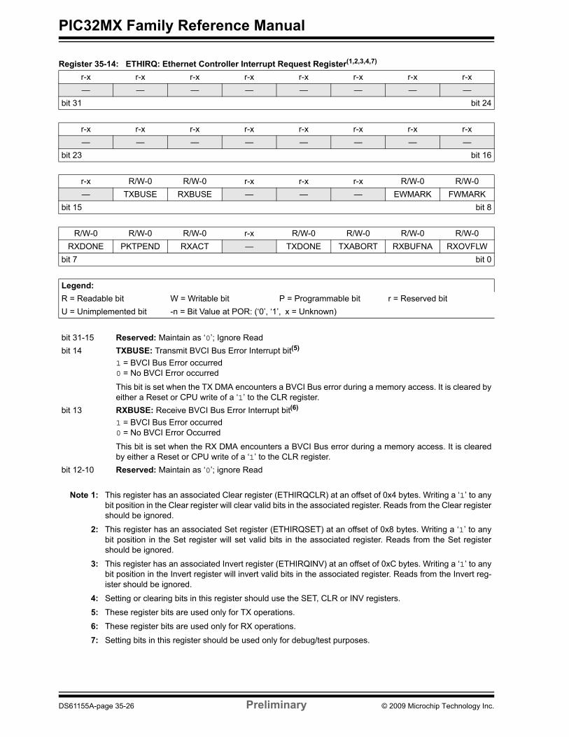
Register 35-14: ETHIRQ: Ethernet Controller Interrupt Request Register(1,2,3,4,7)
r-x r-x r-x r-x r-x r-x r-x r-x— — — — — — — —
bit 31 bit 24
r-x r-x r-x r-x r-x r-x r-x r-x— — — — — — — —
bit 23 bit 16
r-x R/W-0 R/W-0 r-x r-x r-x R/W-0 R/W-0— TXBUSE RXBUSE — — — EWMARK FWMARK
bit 15 bit 8
R/W-0 R/W-0 R/W-0 r-x R/W-0 R/W-0 R/W-0 R/W-0RXDONE PKTPEND RXACT — TXDONE TXABORT RXBUFNA RXOVFLW
bit 7 bit 0
Legend:R = Readable bit W = Writable bit P = Programmable bit r = Reserved bitU = Unimplemented bit -n = Bit Value at POR: (‘0’, ‘1’, x = Unknown)
bit 31-15 Reserved: Maintain as ‘0’; Ignore Readbit 14 TXBUSE: Transmit BVCI Bus Error Interrupt bit(5)
1 = BVCI Bus Error occurred0 = No BVCI Error occurred
This bit is set when the TX DMA encounters a BVCI Bus error during a memory access. It is cleared byeither a Reset or CPU write of a ‘1’ to the CLR register.
bit 13 RXBUSE: Receive BVCI Bus Error Interrupt bit(6)
1 = BVCI Bus Error occurred0 = No BVCI Error Occurred
This bit is set when the RX DMA encounters a BVCI Bus error during a memory access. It is clearedby either a Reset or CPU write of a ‘1’ to the CLR register.
bit 12-10 Reserved: Maintain as ‘0’; ignore Read
Note 1: This register has an associated Clear register (ETHIRQCLR) at an offset of 0x4 bytes. Writing a ‘1’ to anybit position in the Clear register will clear valid bits in the associated register. Reads from the Clear registershould be ignored.
2: This register has an associated Set register (ETHIRQSET) at an offset of 0x8 bytes. Writing a ‘1’ to anybit position in the Set register will set valid bits in the associated register. Reads from the Set registershould be ignored.
3: This register has an associated Invert register (ETHIRQINV) at an offset of 0xC bytes. Writing a ‘1’ to anybit position in the Invert register will invert valid bits in the associated register. Reads from the Invert reg-ister should be ignored.
4: Setting or clearing bits in this register should use the SET, CLR or INV registers.
5: These register bits are used only for TX operations.
6: These register bits are used only for RX operations.
7: Setting bits in this register should be used only for debug/test purposes.
DS61155A-page 35-26 Preliminary © 2009 Microchip Technology Inc.

Section 35. Ethernet ControllerEthernet
Controller
35
bit 9 EWMARK: Empty Watermark Interrupt bit(6)
1 = Empty Watermark pointer reached0 = No interrupt pending
This bit is set when the RX Descriptor Buffer Count is less than or equal to the value in the RXEWM(ETHRXWM<0:7>) value. It is cleared by BUFCNT (ETHSTAT<16:23>) being incremented byhardware. Writing a ‘0’ or a ‘1’ has no effect.
bit 8 FWMARK: Full Watermark Interrupt bit(6)
1 = Full Watermark pointer reached0 = No interrupt pending
This bit is set when the RX Descriptor Buffer Count is greater than or equal to the value in the RXFWM(ETHRXWM<16:23>) field. It is cleared by writing the BUFCDEC (ETHCON1<0>) bit to decrement theBUFCNT counter. Writing a ‘0’ or a ‘1’ has no effect.
bit 7 RXDONE: Receive Done Interrupt bit(6)
1 = RX packet was successfully received0 = No interrupt pending
This bit is set whenever an RX packet is successfully received. It is cleared by either a Reset or CPUwrite of a ‘1’ to the CLR register.
bit 6 PKTPEND: Packet Pending Interrupt bit(6)
1 = Received packet pending in memory0 = No receive packet is pending in memory
This bit is set when the BUFCNT counter has a value other than ‘0’. It is cleared by either a Reset orby writing the BUFCDEC bit to decrement the BUFCNT counter. Writing a ‘0’ or a ‘1’ has no effect.
bit 5 RXACT: Receive Activity Interrupt bit(6)
1 = RX packet data was successfully received0 = No interrupt pending
This bit is set whenever RX packet data is stored in the RXBM FIFO. It is cleared by either a Reset orCPU write of a ‘1’ to the CLR register.
bit 4 Reserved: Maintain as ‘0’; Ignore Readbit 3 TXDONE: Transmit Done Interrupt bit(5)
1 = TX packet successfully sent0 = No interrupt pending
This bit is set when the currently transmitted TX packet completes transmission, and the TransmitStatus Vector is loaded into the first descriptor used for the packet. It is cleared by either a Reset orCPU write of a ‘1’ to the CLR register.
Register 35-14: ETHIRQ: Ethernet Controller Interrupt Request Register(1,2,3,4,7) (Continued)
Note 1: This register has an associated Clear register (ETHIRQCLR) at an offset of 0x4 bytes. Writing a ‘1’ to anybit position in the Clear register will clear valid bits in the associated register. Reads from the Clear registershould be ignored.
2: This register has an associated Set register (ETHIRQSET) at an offset of 0x8 bytes. Writing a ‘1’ to anybit position in the Set register will set valid bits in the associated register. Reads from the Set registershould be ignored.
3: This register has an associated Invert register (ETHIRQINV) at an offset of 0xC bytes. Writing a ‘1’ to anybit position in the Invert register will invert valid bits in the associated register. Reads from the Invert reg-ister should be ignored.
4: Setting or clearing bits in this register should use the SET, CLR or INV registers.
5: These register bits are used only for TX operations.
6: These register bits are used only for RX operations.
7: Setting bits in this register should be used only for debug/test purposes.
© 2009 Microchip Technology Inc. Preliminary DS61155A-page 35-27
PIC32MX Family Reference Manual
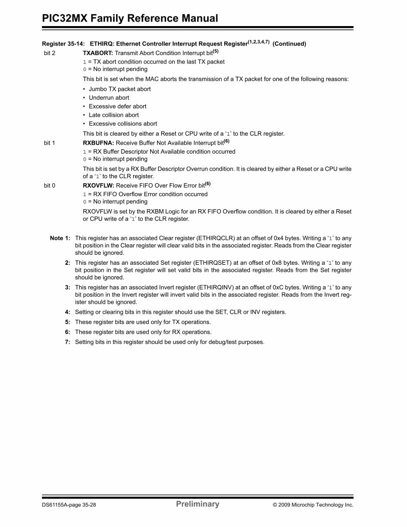
bit 2 TXABORT: Transmit Abort Condition Interrupt bit(5)
1 = TX abort condition occurred on the last TX packet0 = No interrupt pending
This bit is set when the MAC aborts the transmission of a TX packet for one of the following reasons:
• Jumbo TX packet abort• Underrun abort• Excessive defer abort• Late collision abort• Excessive collisions abort
This bit is cleared by either a Reset or CPU write of a ‘1’ to the CLR register.bit 1 RXBUFNA: Receive Buffer Not Available Interrupt bit(6)
1 = RX Buffer Descriptor Not Available condition occurred0 = No interrupt pending
This bit is set by a RX Buffer Descriptor Overrun condition. It is cleared by either a Reset or a CPU writeof a ‘1’ to the CLR register.
bit 0 RXOVFLW: Receive FIFO Over Flow Error bit(6)
1 = RX FIFO Overflow Error condition occurred0 = No interrupt pending
RXOVFLW is set by the RXBM Logic for an RX FIFO Overflow condition. It is cleared by either a Resetor CPU write of a ‘1’ to the CLR register.
Register 35-14: ETHIRQ: Ethernet Controller Interrupt Request Register(1,2,3,4,7) (Continued)
Note 1: This register has an associated Clear register (ETHIRQCLR) at an offset of 0x4 bytes. Writing a ‘1’ to anybit position in the Clear register will clear valid bits in the associated register. Reads from the Clear registershould be ignored.
2: This register has an associated Set register (ETHIRQSET) at an offset of 0x8 bytes. Writing a ‘1’ to anybit position in the Set register will set valid bits in the associated register. Reads from the Set registershould be ignored.
3: This register has an associated Invert register (ETHIRQINV) at an offset of 0xC bytes. Writing a ‘1’ to anybit position in the Invert register will invert valid bits in the associated register. Reads from the Invert reg-ister should be ignored.
4: Setting or clearing bits in this register should use the SET, CLR or INV registers.
5: These register bits are used only for TX operations.
6: These register bits are used only for RX operations.
7: Setting bits in this register should be used only for debug/test purposes.
DS61155A-page 35-28 Preliminary © 2009 Microchip Technology Inc.

Section 35. Ethernet ControllerEthernet
Controller
35
Register 35-15: ETHSTAT: Ethernet Controller Status Register r-x r-x r-x r-x r-x r-x r-x r-x— — — — — — — —
bit 31 bit 24
R/W-0 R/W-0 R/W-0 R/W-0 R/W-0 R/W-0 R/W-0 R/W-0BUFCNT<7:0>(1)
bit 23 bit 16
r-x r-x r-x r-x r-x r-x r-x r-x— — — — — — — —
bit 15 bit 8
R/W-0 R/W-0 R/W-0 r-x r-x r-x r-x r-xETHBUSY(5) TXBUSY(2,6) RXBUSY(3,6) — — — — —bit 7 bit 0
Legend:R = Readable bit W = Writable bit P = Programmable bit r = Reserved bitU = Unimplemented bit -n = Bit Value at POR: (‘0’, ‘1’, x = Unknown)
bit 31-24 Reserved: Maintain as ‘0’; ignore readbit 23-16 BUFCNT<7:0>: Packet Buffer Count bits(1)
Number of packet buffers received in memory. Once a packet has been successfully received, thisregister is incremented by hardware based on the number of descriptors used by the packet. Softwaredecrements the counter (by writing to the BUFCDEC (ETHCON1<0>) bit for each descriptor used) aftera packet has been read out of the buffer. The register does not roll over (0xFF to 0x00) when hardwaretries to increment the register and the register is already at 0xFF. Conversely, the register does not rollunder (0x00 to 0xFF) when software tries to decrement the register and the register is already at0x0000. When software attempts to decrement the counter at the same time that the hardware attemptsto increment the counter, the counter value will remain unchanged.
When this register value reaches 0xFF, the RX logic will halt (ONLY if Auto Flow Control is enabled)awaiting software to write the BUFCDEC bit in order to decrement the register below 0xFF.
If Auto Flow Control is disabled, the RXDMA will continue processing and the BUFCNT will saturate ata value of 0xFF.
When this register is non-zero, the PKTPEND status bit will be set and an interrupt may be generated,depending on the value of the ETHIEN<PKTPENDIE> register bit.
When the ETHRXST register is written, the BUFCNT counter is automatically cleared to 0x00.
Note: BUFCNT will NOT be cleared when ON is set to ‘0’. This enables software to continue toutilize and decrement this count.
bit 15-8 Reserved: Maintain as ‘0’; ignore read
Note 1: These bits are used for RX operations only.
2: This bit is only affected by TX operations.
3: This bit is only affected by RX operations.
4: This bit is affected by TX and RX operations.
5: This bit will be set when ON (ETHCON1<15>) = 1.
6: This bit will be cleared when ON (ETHCON1<15>) = 0.
© 2009 Microchip Technology Inc. Preliminary DS61155A-page 35-29

PIC32MX Family Reference Manual
bit 7 ETHBUSY: Ethernet Module busy bit(5)
1 = Ethernet logic has been turned on (ON (ETHCON1<15>) = 1) or is completing a transaction0 = Ethernet logic is idle
This bit indicates that the module has been turned on or is completing a transaction after being turnedoff.
bit 6 TXBUSY: Transmit Busy bit(2,6)
1 = TX logic is receiving data0 = TX logic is idle
This bit indicates that a packet is currently being transmitted. A change in this status bit is notnecessarily reflected by the TXDONE interrupt, as TX packets may be aborted or rejected by the MAC.
bit 5 RXBUSY: Receive Busy bit(3,6)
1 = RX logic is receiving data0 = RX logic is idle
This bit indicates that a packet is currently being received. A change in this status bit is not necessarilyreflected by the RXDONE interrupt, as RX packets may be aborted or rejected by the RX filter.
bit 4-0 Reserved: Maintain as ‘0’; ignore read
Register 35-15: ETHSTAT: Ethernet Controller Status Register (Continued)
Note 1: These bits are used for RX operations only.
2: This bit is only affected by TX operations.
3: This bit is only affected by RX operations.
4: This bit is affected by TX and RX operations.
5: This bit will be set when ON (ETHCON1<15>) = 1.
6: This bit will be cleared when ON (ETHCON1<15>) = 0.
DS61155A-page 35-30 Preliminary © 2009 Microchip Technology Inc.

Section 35. Ethernet ControllerEthernet
Controller
35
Register 35-16: ETHRXOVFLOW : Ethernet Controller Receive Overflow Statistics Register(1,2,3,4,5,6)
r-x r-x r-x r-x r-x r-x r-x r-x— — — — — — — —
bit 31 bit 24
r-x r-x r-x r-x r-x r-x r-x r-x— — — — — — — —
bit 23 bit 16
R/W-0 R/W-0 R/W-0 R/W-0 R/W-0 R/W-0 R/W-0 R/W-0RXOVFLWCNT<15:8>
bit 15 bit 8
R/W-0 R/W-0 R/W-0 R/W-0 R/W-0 R/W-0 R/W-0 R/W-0RXOVFLWCNT<7:0>
bit 7 bit 0
Legend:R = Readable bit W = Writable bit P = Programmable bit r = Reserved bitU = Unimplemented bit -n = Bit Value at POR: (‘0’, ‘1’, x = Unknown)
bit 31-16 Reserved: Maintain as ‘0’; ignore readbit 15-0 RXOVFLWCNT<15:0>: Dropped Receive Frames Count bits
Increment counter for frames accepted by the RX filter and subsequently dropped due to internalreceive error (RXFIFO overrun). This event also sets the RXOVFLW (ETHIRQ<0>) interrupt flag.
Note 1: This register has an associated Clear register (ETHRXOVFLOWCLR) at an offset of 0x4 bytes. Writing a‘1’ to any bit position in the Clear register will clear valid bits in the associated register. Reads from theClear register should be ignored.
2: This register has an associated Set register (ETHRXOVFLOWSET) at an offset of 0x8 bytes. Writing a ‘1’to any bit position in the Set register will set valid bits in the associated register. Reads from the Set registershould be ignored.
3: This register has an associated Invert register (ETHRXOVFLOWINV) at an offset of 0xC bytes. Writing a‘1’ to any bit position in the Invert register will invert valid bits in the associated register. Reads from theInvert register should be ignored.
4: This register is used for RX operations only.
5: This register is automatically cleared by hardware after a read operation, unless the byte enables for bytes0/1 are ‘0’.
6: Setting the bits in this register should be only used for debug/test purposes.
© 2009 Microchip Technology Inc. Preliminary DS61155A-page 35-31

PIC32MX Family Reference Manual
Register 35-17: ETHFRMTXOK : Ethernet Controller Frames Transmitted OK Statistics Register(1,2,3,4,5,6)
r-x r-x r-x r-x r-x r-x r-x r-x— — — — — — — —
bit 31 bit 24
r-x r-x r-x r-x r-x r-x r-x r-x— — — — — — — —
bit 23 bit 16
R/W-0 R/W-0 R/W-0 R/W-0 R/W-0 R/W-0 R/W-0 R/W-0FRMTXOKCNT<15:8>
bit 15 bit 8
R/W-0 R/W-0 R/W-0 R/W-0 R/W-0 R/W-0 R/W-0 R/W-0FRMTXOKCNT<7:0>
bit 7 bit 0
Legend:R = Readable bit W = Writable bit P = Programmable bit r = Reserved bitU = Unimplemented bit -n = Bit Value at POR: (‘0’, ‘1’, x = Unknown)
bit 31-16 Reserved: Maintain as ‘0’; ignore readbit 15-0 FRMTXOKCNT<15:0>: Frame Transmitted OK Count bits
Increment counter for frames successfully transmitted.
Note 1: This register has an associated Clear register (ETHFRMTXOKCLR) at an offset of 0x4 bytes. Writing a ‘1’to any bit position in the Clear register will clear valid bits in the associated register. Reads from the Clearregister should be ignored.
2: This register has an associated Set register (ETHFRMTXOKSET) at an offset of 0x8 bytes. Writing a ‘1’to any bit position in the Set register will set valid bits in the associated register. Reads from the Set registershould be ignored.
3: This register has an associated Invert register (ETHFRMTXOKINV) at an offset of 0xC bytes. Writing a ‘1’to any bit position in the Invert register will invert valid bits in the associated register. Reads from the Invertregister should be ignored.
4: This register is used for TX operations only.
5: This register is automatically cleared by hardware after a read operation, unless the byte enables for bytes0/1 are ‘0’.
6: Setting the bits in this register should be only used for debug/test purposes.
DS61155A-page 35-32 Preliminary © 2009 Microchip Technology Inc.

Section 35. Ethernet ControllerEthernet
Controller
35
Register 35-18: ETHSCOLFRM : Ethernet Controller Single Collision Frames Statistics Register(1,2,3,4,5,6)
r-x r-x r-x r-x r-x r-x r-x r-x— — — — — — — —
bit 31 bit 24
r-x r-x r-x r-x r-x r-x r-x r-x— — — — — — — —
bit 23 bit 16
R/W-0 R/W-0 R/W-0 R/W-0 R/W-0 R/W-0 R/W-0 R/W-0SCOLFRMCNT<15:8>
bit 15 bit 8
R/W-0 R/W-0 R/W-0 R/W-0 R/W-0 R/W-0 R/W-0 R/W-0SCOLFRMCNT<7:0>
bit 7 bit 0
Legend:R = Readable bit W = Writable bit P = Programmable bit r = Reserved bitU = Unimplemented bit -n = Bit Value at POR: (‘0’, ‘1’, x = Unknown)
bit 31-16 Reserved: Maintain as ‘0’; ignore readbit 15-0 SCOLFRMCNT<15:0>: Single Collision Frame Count bits
Increment count for frames that were successfully transmitted on the second try.
Note 1: This register has an associated Clear register (ETHSCOLFRMCLR) at an offset of 0x4 bytes. Writing a ‘1’to any bit position in the Clear register will clear valid bits in the associated register. Reads from the Clearregister should be ignored.
2: This register has an associated Set register (ETHSCOLFRMSET) at an offset of 0x8 bytes. Writing a ‘1’to any bit position in the Set register will set valid bits in the associated register. Reads from the Set registershould be ignored.
3: This register has an associated Invert register (ETHSCOLFRMINV) at an offset of 0xC bytes. Writing a ‘1’to any bit position in the Invert register will invert valid bits in the associated register. Reads from the Invertregister should be ignored.
4: This register is used for TX operations only.
5: This register is automatically cleared by hardware after a read operation, unless the byte enables for bytes0/1 are ‘0’.
6: Setting the bits in this register should be only used for debug/test purposes.
© 2009 Microchip Technology Inc. Preliminary DS61155A-page 35-33
PIC32MX Family Reference Manual
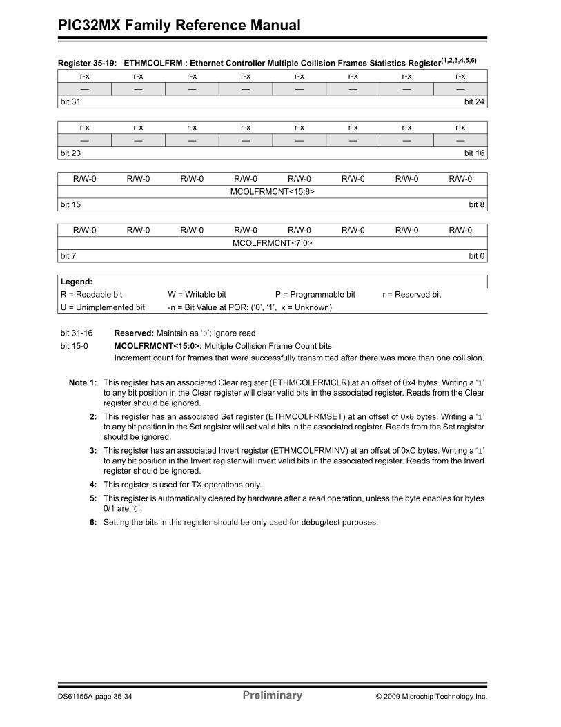
Register 35-19: ETHMCOLFRM : Ethernet Controller Multiple Collision Frames Statistics Register(1,2,3,4,5,6)
r-x r-x r-x r-x r-x r-x r-x r-x— — — — — — — —
bit 31 bit 24
r-x r-x r-x r-x r-x r-x r-x r-x— — — — — — — —
bit 23 bit 16
R/W-0 R/W-0 R/W-0 R/W-0 R/W-0 R/W-0 R/W-0 R/W-0MCOLFRMCNT<15:8>
bit 15 bit 8
R/W-0 R/W-0 R/W-0 R/W-0 R/W-0 R/W-0 R/W-0 R/W-0MCOLFRMCNT<7:0>
bit 7 bit 0
Legend:R = Readable bit W = Writable bit P = Programmable bit r = Reserved bitU = Unimplemented bit -n = Bit Value at POR: (‘0’, ‘1’, x = Unknown)
bit 31-16 Reserved: Maintain as ‘0’; ignore readbit 15-0 MCOLFRMCNT<15:0>: Multiple Collision Frame Count bits
Increment count for frames that were successfully transmitted after there was more than one collision.
Note 1: This register has an associated Clear register (ETHMCOLFRMCLR) at an offset of 0x4 bytes. Writing a ‘1’to any bit position in the Clear register will clear valid bits in the associated register. Reads from the Clearregister should be ignored.
2: This register has an associated Set register (ETHMCOLFRMSET) at an offset of 0x8 bytes. Writing a ‘1’to any bit position in the Set register will set valid bits in the associated register. Reads from the Set registershould be ignored.
3: This register has an associated Invert register (ETHMCOLFRMINV) at an offset of 0xC bytes. Writing a ‘1’to any bit position in the Invert register will invert valid bits in the associated register. Reads from the Invertregister should be ignored.
4: This register is used for TX operations only.
5: This register is automatically cleared by hardware after a read operation, unless the byte enables for bytes0/1 are ‘0’.
6: Setting the bits in this register should be only used for debug/test purposes.
DS61155A-page 35-34 Preliminary © 2009 Microchip Technology Inc.

Section 35. Ethernet ControllerEthernet
Controller
35
Register 35-20: ETHFRMRXOK : Ethernet Controller Frames Received OK Statistics Register(1,2,3,4,5,6)
r-x r-x r-x r-x r-x r-x r-x r-x— — — — — — — —
bit 31 bit 24
r-x r-x r-x r-x r-x r-x r-x r-x— — — — — — — —
bit 23 bit 16
R/W-0 R/W-0 R/W-0 R/W-0 R/W-0 R/W-0 R/W-0 R/W-0FRMRXOKCNT<15:8>
bit 15 bit 8
R/W-0 R/W-0 R/W-0 R/W-0 R/W-0 R/W-0 R/W-0 R/W-0FRMRXOKCNT<7:0>
bit 7 bit 0
Legend:R = Readable bit W = Writable bit P = Programmable bit r = Reserved bitU = Unimplemented bit -n = Bit Value at POR: (‘0’, ‘1’, x = Unknown)
bit 31-16 Reserved: Maintain as ‘0’; ignore readbit 15-0 FRMRXOKCNT<15:0>: Frames Received OK Count bits
Increment count for frames received successfully by the RX Filter. This count will not be incremented ifthere is a Frame Check Sequence (FCS) or Alignment error.
Note 1: This register has an associated Clear register (ETHFRMRXOKCLR) at an offset of 0x4 bytes. Writing a ‘1’to any bit position in the Clear register will clear valid bits in the associated register. Reads from the Clearregister should be ignored.
2: This register has an associated Set register (ETHFRMRXOKSET) at an offset of 0x8 bytes. Writing a ‘1’to any bit position in the Set register will set valid bits in the associated register. Reads from the Set registershould be ignored.
3: This register has an associated Invert register (ETHFRMRXOKINV) at an offset of 0xC bytes. Writing a ‘1’to any bit position in the Invert register will invert valid bits in the associated register. Reads from the Invertregister should be ignored.
4: This register is used for RX operations only.
5: This register is automatically cleared by hardware after a read operation, unless the byte enables for bytes0/1 are ‘0’.
6: Setting the bits in this register should be only used for debug/test purposes.
© 2009 Microchip Technology Inc. Preliminary DS61155A-page 35-35
PIC32MX Family Reference Manual
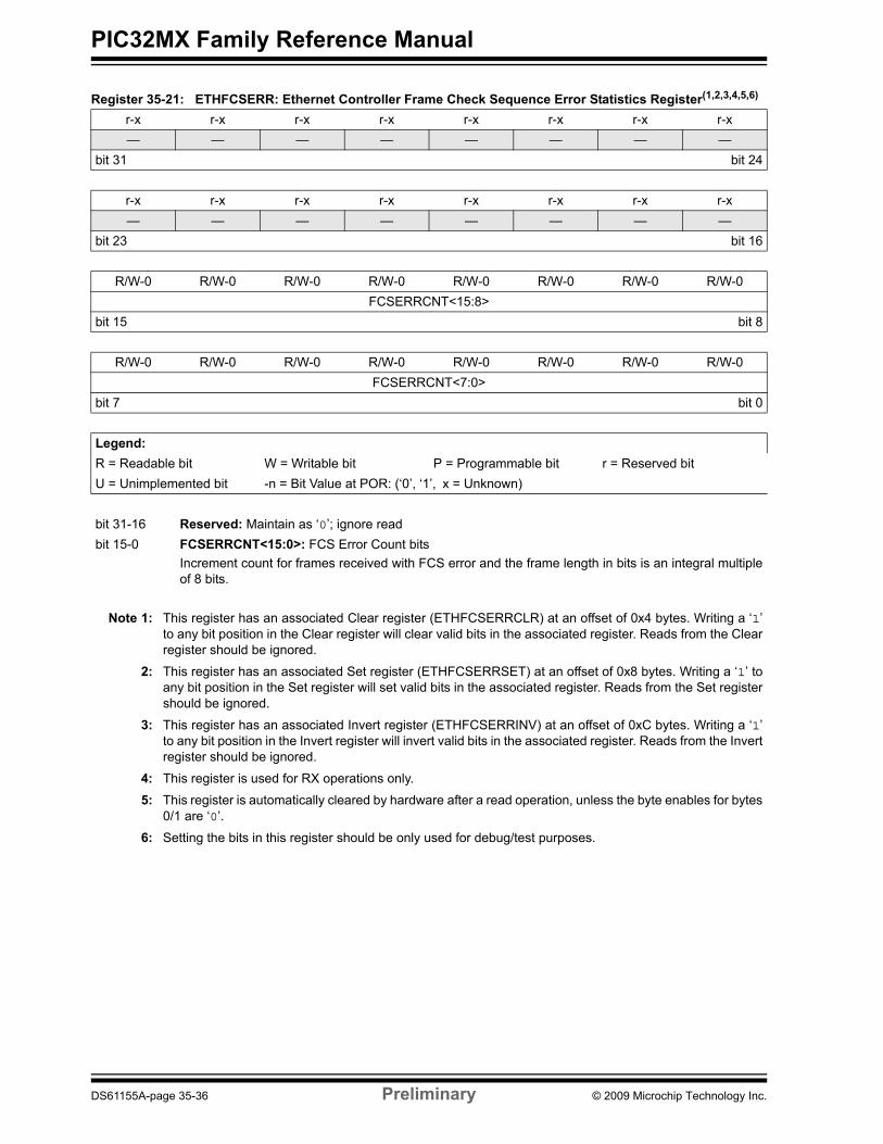
Register 35-21: ETHFCSERR: Ethernet Controller Frame Check Sequence Error Statistics Register(1,2,3,4,5,6)
r-x r-x r-x r-x r-x r-x r-x r-x— — — — — — — —
bit 31 bit 24
r-x r-x r-x r-x r-x r-x r-x r-x— — — — — — — —
bit 23 bit 16
R/W-0 R/W-0 R/W-0 R/W-0 R/W-0 R/W-0 R/W-0 R/W-0FCSERRCNT<15:8>
bit 15 bit 8
R/W-0 R/W-0 R/W-0 R/W-0 R/W-0 R/W-0 R/W-0 R/W-0FCSERRCNT<7:0>
bit 7 bit 0
Legend:R = Readable bit W = Writable bit P = Programmable bit r = Reserved bitU = Unimplemented bit -n = Bit Value at POR: (‘0’, ‘1’, x = Unknown)
bit 31-16 Reserved: Maintain as ‘0’; ignore readbit 15-0 FCSERRCNT<15:0>: FCS Error Count bits
Increment count for frames received with FCS error and the frame length in bits is an integral multipleof 8 bits.
Note 1: This register has an associated Clear register (ETHFCSERRCLR) at an offset of 0x4 bytes. Writing a ‘1’to any bit position in the Clear register will clear valid bits in the associated register. Reads from the Clearregister should be ignored.
2: This register has an associated Set register (ETHFCSERRSET) at an offset of 0x8 bytes. Writing a ‘1’ toany bit position in the Set register will set valid bits in the associated register. Reads from the Set registershould be ignored.
3: This register has an associated Invert register (ETHFCSERRINV) at an offset of 0xC bytes. Writing a ‘1’to any bit position in the Invert register will invert valid bits in the associated register. Reads from the Invertregister should be ignored.
4: This register is used for RX operations only.
5: This register is automatically cleared by hardware after a read operation, unless the byte enables for bytes0/1 are ‘0’.
6: Setting the bits in this register should be only used for debug/test purposes.
DS61155A-page 35-36 Preliminary © 2009 Microchip Technology Inc.

Section 35. Ethernet ControllerEthernet
Controller
35
Register 35-22: ETHALGNERR: Ethernet Controller Alignment Errors Statistics Register(1,2,3,4,5,6)
r-x r-x r-x r-x r-x r-x r-x r-x— — — — — — — —
bit 31 bit 24
r-x r-x r-x r-x r-x r-x r-x r-x— — — — — — — —
bit 23 bit 16
R/W-0 R/W-0 R/W-0 R/W-0 R/W-0 R/W-0 R/W-0 R/W-0ALGNERRCNT<15:8>
bit 15 bit 8
R/W-0 R/W-0 R/W-0 R/W-0 R/W-0 R/W-0 R/W-0 R/W-0ALGNERRCNT<7:0>
bit 7 bit 0
Legend:R = Readable bit W = Writable bit P = Programmable bit r = Reserved bitU = Unimplemented bit -n = Bit Value at POR: (‘0’, ‘1’, x = Unknown)
bit 31-16 Reserved: Maintain as ‘0’; ignore readbit 15-0 ALGNERRCNT<15:0>: Alignment Error Count bits
Increment count for frames with alignment errors. Note that an alignment error is a frame that has anFCS error and the frame length in bits is not an integral multiple of 8 bits (a.k.a., dribble nibble)
Note 1: This register has an associated Clear register (ETHALGNERRCLR) at an offset of 0x4 bytes. Writing a ‘1’to any bit position in the Clear register will clear valid bits in the associated register. Reads from the Clearregister should be ignored.
2: This register has an associated Set register (ETHALGNERRSET) at an offset of 0x8 bytes. Writing a ‘1’ toany bit position in the Set register will set valid bits in the associated register. Reads from the Set registershould be ignored.
3: This register has an associated Invert register (ETHALGNERRINV) at an offset of 0xC bytes. Writing a ‘1’to any bit position in the Invert register will invert valid bits in the associated register. Reads from the Invertregister should be ignored.
4: This register is used for RX operations only.
5: This register is automatically cleared by hardware after a read operation, unless the byte enables for bytes0/1 are ‘0’.
6: Setting the bits in this register should be only used for debug/test purposes.
© 2009 Microchip Technology Inc. Preliminary DS61155A-page 35-37

PIC32MX Family Reference Manual
Register 35-23: EMACxCFG1: Ethernet Controller MAC Configuration 1 Register(1,2,3,4)
r-x r-x r-x r-x r-x r-x r-x r-x— — — — — — — —
bit 31 bit 24
r-x r-x r-x r-x r-x r-x r-x r-x— — — — — — — —
bit 23 bit 16
R/W-1 R/W-0 r-x r-x R/W-0 R/W-0 R/W-0 R/W-0SOFTRESET SIMRESET — — RESETRMCS RESETRFUN RESETTMCS RESETTFUNbit 15 bit 8
r-x r-x r-x R/W-0 R/W-1 R/W-1 R/W-0 R/W-1— — — LOOPBACK TXPAUSE RXPAUSE PASSALL RXENABLE
bit 7 bit 0
Legend:R = Readable bit W = Writable bit P = Programmable bit r = Reserved bitU = Unimplemented bit -n = Bit Value at POR: (‘0’, ‘1’, x = Unknown)
bit 31-16 Reserved: Maintain as ‘0’; ignore readbit 15 SOFTRESET: Soft Reset bit
Setting this bit will put the MACMII in reset. Its default value is ‘1’.bit 14 SIMRESET: Simulation Reset bit
Setting this bit will cause a reset to the random number generator within the Transmit Function.bit 13-12 Reserved: Maintain as ‘0’; ignore readbit 11 RESETRMCS: Reset MCS/RX bit
Setting this bit will put the MAC Control Sub-layer/Receive domain logic in reset.bit 10 RESETRFUN: Reset RX Function bit
Setting this bit will put the MAC Receive function logic in reset.bit 9 RESETTMCS: Reset MCS/TX bit
Setting this bit will put the MAC Control Sub-layer/TX domain logic in reset.bit 8 RESETTFUN: Reset TX Function bit
Setting this bit will put the MAC Transmit function logic in reset.bit 7-5 Reserved: Maintain as ‘0’; ignore read
Note 1: This register has an associated Clear register (EMACxCFG1CLR) at an offset of 0x4 bytes. Writing a ‘1’to any bit position in the Clear register will clear valid bits in the associated register. Reads from the Clearregister should be ignored.
2: This register has an associated Set register (EMACxCFG1SET) at an offset of 0x8 bytes. Writing a ‘1’ toany bit position in the Set register will set valid bits in the associated register. Reads from the Set registershould be ignored.
3: This register has an associated Invert register (EMACxCFG1INV) at an offset of 0xC bytes. Writing a ‘1’to any bit position in the Invert register will invert valid bits in the associated register. Reads from the Invertregister should be ignored.
4: Both 16- and 32-bit accesses are allowed to these registers (including the Set, Clear and Invert registers).8-bit accesses are not allowed and are ignored by the hardware.
DS61155A-page 35-38 Preliminary © 2009 Microchip Technology Inc.

Section 35. Ethernet ControllerEthernet
Controller
35
bit 4 LOOPBACK: MAC Loopback mode bit1 = MAC Transmit interface is loop backed to the MAC Receive interface0 = MAC normal operation
bit 3 TXPAUSE: MAC TX Flow Control bit1 = PAUSE Flow Control frames are allowed to be transmitted0 = PAUSE Flow Control frames are blocked
bit 2 RXPAUSE: MAC RX Flow Control bit1 = The MAC acts upon received PAUSE Flow Control frames0 = Received PAUSE Flow Control frames are ignored
bit 1 PASSALL: MAC Pass all Receive Frames bit1 = The MAC will accept all frames regardless of type (normal vs. Control)0 = The received Control frames are ignored
bit 0 RXENABLE: MAC Receive Enable bit1 = Enable the MAC receiving of frames0 = Disable the MAC receiving of frames
Register 35-23: EMACxCFG1: Ethernet Controller MAC Configuration 1 Register(1,2,3,4) (Continued)
Note 1: This register has an associated Clear register (EMACxCFG1CLR) at an offset of 0x4 bytes. Writing a ‘1’to any bit position in the Clear register will clear valid bits in the associated register. Reads from the Clearregister should be ignored.
2: This register has an associated Set register (EMACxCFG1SET) at an offset of 0x8 bytes. Writing a ‘1’ toany bit position in the Set register will set valid bits in the associated register. Reads from the Set registershould be ignored.
3: This register has an associated Invert register (EMACxCFG1INV) at an offset of 0xC bytes. Writing a ‘1’to any bit position in the Invert register will invert valid bits in the associated register. Reads from the Invertregister should be ignored.
4: Both 16- and 32-bit accesses are allowed to these registers (including the Set, Clear and Invert registers).8-bit accesses are not allowed and are ignored by the hardware.
© 2009 Microchip Technology Inc. Preliminary DS61155A-page 35-39
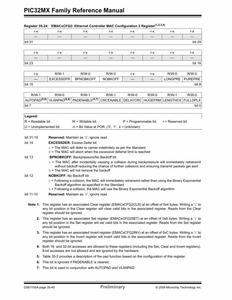
PIC32MX Family Reference Manual
Register 35-24: EMACxCFG2: Ethernet Controller MAC Configuration 2 Register(1,2,3,4)
r-x r-x r-x r-x r-x r-x r-x r-x— — — — — — — —
bit 31 bit 24
r-x r-x r-x r-x r-x r-x r-x r-x— — — — — — — —
bit 23 bit 16
r-x R/W-1 R/W-0 R/W-0 r-x r-x R/W-0 R/W-0— EXCESSDFR BPNOBKOFF NOBKOFF — — LONGPRE PUREPRE
bit 15 bit 8
R/W-1 R/W-0 R/W-1 R/W-1 R/W-0 R/W-0 R/W-1 R/W-0AUTOPAD(5,6) VLANPAD(5,6) PADENABLE(5,7) CRCENABLE DELAYCRC HUGEFRM LENGTHCK FULLDPLXbit 7 bit 0
Legend:R = Readable bit W = Writable bit P = Programmable bit r = Reserved bitU = Unimplemented bit -n = Bit Value at POR: (‘0’, ‘1’, x = Unknown)
bit 31-15 Reserved: Maintain as ‘0’; ignore readbit 14 EXCESSDER: Excess Defer bit
1 = The MAC will defer to carrier indefinitely as per the Standard0 = The MAC will abort when the excessive deferral limit is reached
bit 13 BPNOBKOFF: Backpressure/No Backoff bit1 = The MAC after incidentally causing a collision during backpressure will immediately retransmit
without backoff reducing the chance of further collisions and ensuring transmit packets get sent0 = The MAC will not remove the backoff
bit 12 NOBKOFF: No Backoff bit1 = Following a collision, the MAC will immediately retransmit rather than using the Binary Exponential
Backoff algorithm as specified in the Standard0 = Following a collision, the MAC will use the Binary Exponential Backoff algorithm
bit 11-10 Reserved: Maintain as ‘0’; ignore read
Note 1: This register has an associated Clear register (EMACxCFG2CLR) at an offset of 0x4 bytes. Writing a ‘1’ toany bit position in the Clear register will clear valid bits in the associated register. Reads from the Clearregister should be ignored.
2: This register has an associated Set register (EMACxCFG2SET) at an offset of 0x8 bytes. Writing a ‘1’ toany bit position in the Set register will set valid bits in the associated register. Reads from the Set registershould be ignored.
3: This register has an associated Invert register (EMACxCFG2INV) at an offset of 0xC bytes. Writing a ‘1’ toany bit position in the Invert register will invert valid bits in the associated register. Reads from the Invertregister should be ignored.
4: Both 16- and 32-bit accesses are allowed to these registers (including the Set, Clear and Invert registers).8-bit accesses are not allowed and are ignored by the hardware.
5: Table 35-2 provides a description of the pad function based on the configuration of this register.
6: This bit is ignored if PADENABLE is cleared.
7: This bit is used in conjunction with AUTOPAD and VLANPAD.
DS61155A-page 35-40 Preliminary © 2009 Microchip Technology Inc.
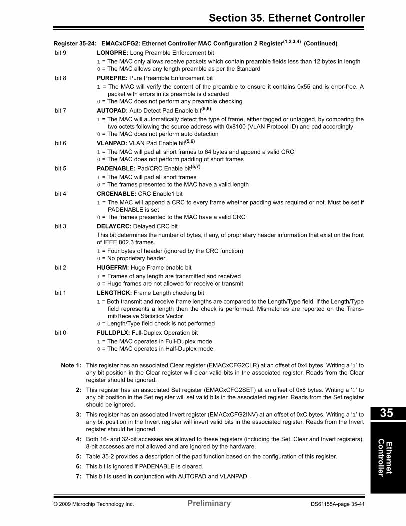
Section 35. Ethernet ControllerEthernet
Controller
35
bit 9 LONGPRE: Long Preamble Enforcement bit1 = The MAC only allows receive packets which contain preamble fields less than 12 bytes in length0 = The MAC allows any length preamble as per the Standard
bit 8 PUREPRE: Pure Preamble Enforcement bit1 = The MAC will verify the content of the preamble to ensure it contains 0x55 and is error-free. A
packet with errors in its preamble is discarded0 = The MAC does not perform any preamble checking
bit 7 AUTOPAD: Auto Detect Pad Enable bit(5,6)
1 = The MAC will automatically detect the type of frame, either tagged or untagged, by comparing thetwo octets following the source address with 0x8100 (VLAN Protocol ID) and pad accordingly
0 = The MAC does not perform auto detectionbit 6 VLANPAD: VLAN Pad Enable bit(5,6)
1 = The MAC will pad all short frames to 64 bytes and append a valid CRC0 = The MAC does not perform padding of short frames
bit 5 PADENABLE: Pad/CRC Enable bit(5,7)
1 = The MAC will pad all short frames0 = The frames presented to the MAC have a valid length
bit 4 CRCENABLE: CRC Enable1 bit1 = The MAC will append a CRC to every frame whether padding was required or not. Must be set if
PADENABLE is set0 = The frames presented to the MAC have a valid CRC
bit 3 DELAYCRC: Delayed CRC bitThis bit determines the number of bytes, if any, of proprietary header information that exist on the frontof IEEE 802.3 frames.1 = Four bytes of header (ignored by the CRC function)0 = No proprietary header
bit 2 HUGEFRM: Huge Frame enable bit1 = Frames of any length are transmitted and received0 = Huge frames are not allowed for receive or transmit
bit 1 LENGTHCK: Frame Length checking bit1 = Both transmit and receive frame lengths are compared to the Length/Type field. If the Length/Type
field represents a length then the check is performed. Mismatches are reported on the Trans-mit/Receive Statistics Vector
0 = Length/Type field check is not performedbit 0 FULLDPLX: Full-Duplex Operation bit
1 = The MAC operates in Full-Duplex mode0 = The MAC operates in Half-Duplex mode
Register 35-24: EMACxCFG2: Ethernet Controller MAC Configuration 2 Register(1,2,3,4) (Continued)
Note 1: This register has an associated Clear register (EMACxCFG2CLR) at an offset of 0x4 bytes. Writing a ‘1’ toany bit position in the Clear register will clear valid bits in the associated register. Reads from the Clearregister should be ignored.
2: This register has an associated Set register (EMACxCFG2SET) at an offset of 0x8 bytes. Writing a ‘1’ toany bit position in the Set register will set valid bits in the associated register. Reads from the Set registershould be ignored.
3: This register has an associated Invert register (EMACxCFG2INV) at an offset of 0xC bytes. Writing a ‘1’ toany bit position in the Invert register will invert valid bits in the associated register. Reads from the Invertregister should be ignored.
4: Both 16- and 32-bit accesses are allowed to these registers (including the Set, Clear and Invert registers).8-bit accesses are not allowed and are ignored by the hardware.
5: Table 35-2 provides a description of the pad function based on the configuration of this register.
6: This bit is ignored if PADENABLE is cleared.
7: This bit is used in conjunction with AUTOPAD and VLANPAD.
© 2009 Microchip Technology Inc. Preliminary DS61155A-page 35-41
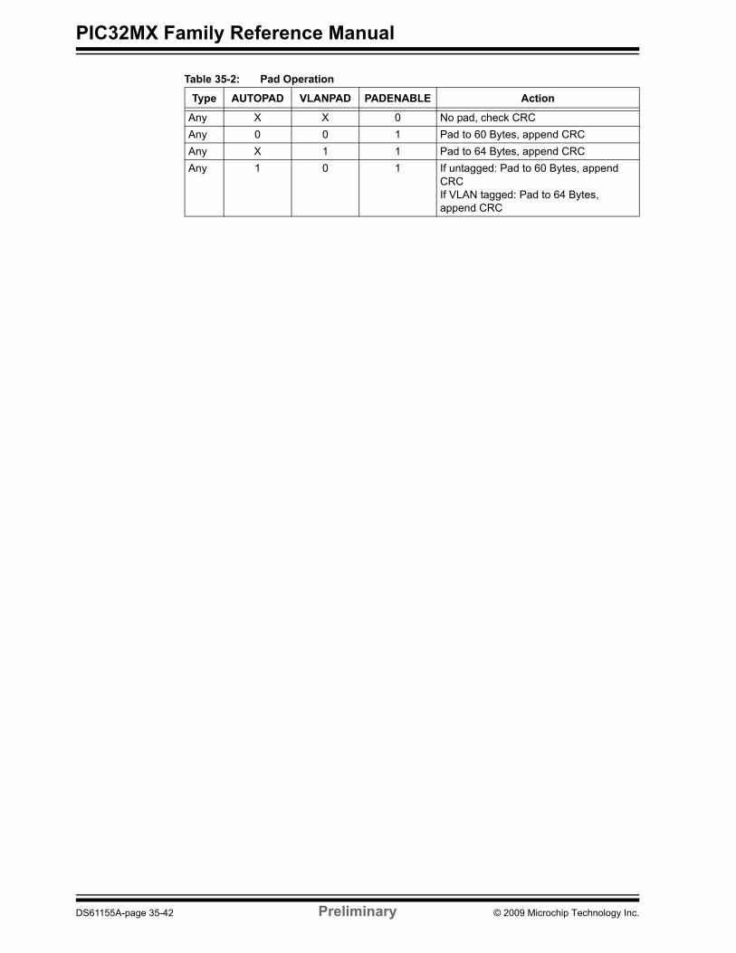
PIC32MX Family Reference Manual
Table 35-2: Pad Operation
Type AUTOPAD VLANPAD PADENABLE Action
Any X X 0 No pad, check CRCAny 0 0 1 Pad to 60 Bytes, append CRCAny X 1 1 Pad to 64 Bytes, append CRCAny 1 0 1 If untagged: Pad to 60 Bytes, append
CRCIf VLAN tagged: Pad to 64 Bytes, append CRC
DS61155A-page 35-42 Preliminary © 2009 Microchip Technology Inc.

Section 35. Ethernet ControllerEthernet
Controller
35
Register 35-25: EMACxIPGT: Ethernet Controller MAC Back-to-Back Interpacket Gap Register(1,2,3,4)
r-x r-x r-x r-x r-x r-x r-x r-x— — — — — — — —
bit 31 bit 24
r-x r-x r-x r-x r-x r-x r-x r-x— — — — — — — —
bit 23 bit 16
r-x r-x r-x r-x r-x r-x r-x r-x— — — — — — — —
bit 15 bit 8
r-x R/W-0 R/W-0 R/W-1 R/W-0 R/W-0 R/W-1 R/W-0— B2BIPKTGP<6:0>
bit 7 bit 0
Legend:R = Readable bit W = Writable bit P = Programmable bit r = Reserved bitU = Unimplemented bit -n = Bit Value at POR: (‘0’, ‘1’, x = Unknown)
bit 31-7 Reserved: Maintain as ‘0’; ignore readbit 6-0 B2BIPKTGP<6:0>: Back-to-Back Interpacket Gap bits
This is a programmable field representing the nibble time offset of the minimum possible periodbetween the end of any transmitted packet, to the beginning of the next. In Full-Duplex mode, the reg-ister value should be the desired period in nibble times minus 3. In Half-Duplex mode, the register valueshould be the desired period in nibble times minus 6. In Full-Duplex the recommended setting is 0x15(21d), which represents the minimum IPG of 0.96 µs (in 100 Mbps) or 9.6 µs (in 10 Mbps). InHalf-Duplex mode, the recommended setting is 0x12 (18d), which also represents the minimum IPG of0.96 µs (in 100 Mbps) or 9.6 µs (in 10 Mbps).
Note 1: This register has an associated Clear register (EMACxIPGTCLR) at an offset of 0x4 bytes. Writing a ‘1’ toany bit position in the Clear register will clear valid bits in the associated register. Reads from the Clearregister should be ignored.
2: This register has an associated Set register (EMACxIPGTSET) at an offset of 0x8 bytes. Writing a ‘1’ toany bit position in the Set register will set valid bits in the associated register. Reads from the Set registershould be ignored.
3: This register has an associated Invert register (EMACxIPGTINV) at an offset of 0xC bytes. Writing a ‘1’ toany bit position in the Invert register will invert valid bits in the associated register. Reads from the Invertregister should be ignored.
4: Both 16- and 32-bit accesses are allowed to these registers (including the Set, Clear and Invert registers).8-bit accesses are not allowed and are ignored by the hardware.
© 2009 Microchip Technology Inc. Preliminary DS61155A-page 35-43

PIC32MX Family Reference Manual
Register 35-26: EMACxIPGR: Ethernet Controller MAC Non-Back-to-Back Interpacket Gap Register(1,2,3,4)
r-x r-x r-x r-x r-x r-x r-x r-x— — — — — — — —
bit 31 bit 24
r-x r-x r-x r-x r-x r-x r-x r-x— — — — — — — —
bit 23 bit 16
r-x R/W-0 R/W-0 R/W-0 R/W-1 R/W-1 R/W-0 R/W-0— NB2BIPKTGP1<6:0>
bit 15 bit 8
r-x R/W-0 R/W-0 R/W-1 R/W-0 R/W-0 R/W-1 R/W-0— NB2BIPKTGP2<6:0>
bit 7 bit 0
Legend:R = Readable bit W = Writable bit P = Programmable bit r = Reserved bitU = Unimplemented bit -n = Bit Value at POR: (‘0’, ‘1’, x = Unknown)
bit 31-15 Reserved: Maintain as ‘0’; ignore readbit 14-8 NB2BIPKTGP1<6:0>: Non-Back-to-Back Interpacket Gap Part 1 bits
This is a programmable field representing the optional carrierSense window referenced in IEEE802.3/4.2.3.2.1 ‘Carrier Deference’. If carrier is detected during the timing of IPGR1, the MAC defers tocarrier. If, however, carrier becomes after IPGR1, the MAC continues timing IPGR2 and transmits,knowingly causing a collision, thus ensuring fair access to medium. Its range of values is 0x0 to IPGR2.Its recommend value is 0xC (12d).
bit 7 Reserved: Maintain as ‘0’; ignore readbit 6-0 NB2BIPKTGP2<6:0>: Non-Back-to-Back Interpacket Gap Part 2 bits
This is a programmable field representing the non-back-to-back Inter-Packet-Gap. Its recommendedvalue is 0x12 (18d), which represents the minimum IPG of 0.96 µs (in 100 Mbps) or 9.6 µs (in 10 Mbps).
Note 1: This register has an associated Clear register (EMACxIPGRCLR) at an offset of 0x4 bytes. Writing a ‘1’ toany bit position in the Clear register will clear valid bits in the associated register. Reads from the Clearregister should be ignored.
2: This register has an associated Set register (EMACxIPGRSET) at an offset of 0x8 bytes. Writing a ‘1’ toany bit position in the Set register will set valid bits in the associated register. Reads from the Set registershould be ignored.
3: This register has an associated Invert register (EMACxIPGRINV) at an offset of 0xC bytes. Writing a ‘1’ toany bit position in the Invert register will invert valid bits in the associated register. Reads from the Invertregister should be ignored.
4: Both 16- and 32-bit accesses are allowed to these registers (including the Set, Clear and Invert registers).8-bit accesses are not allowed and are ignored by the hardware.
DS61155A-page 35-44 Preliminary © 2009 Microchip Technology Inc.

Section 35. Ethernet ControllerEthernet
Controller
35
Register 35-27: EMACxCLRT: Ethernet Controller MAC Collision Window/Retry Limit Register(1,2,3,4)
r-x r-x r-x r-x r-x r-x r-x r-x— — — — — — — —
bit 31 bit 24
r-x r-x r-x r-x r-x r-x r-x r-x— — — — — — — —
bit 23 bit 16
r-x r-x R/W-1 R/W-1 R/W-0 R/W-1 R/W-1 R/W-1— — CWINDOW<5:0>
bit 15 bit 8
r-x r-x r-x r-x R/W-1 R/W-1 R/W-1 R/W-1— — — — RETX<3:0>
bit 7 bit 0
Legend:R = Readable bit W = Writable bit P = Programmable bit r = Reserved bitU = Unimplemented bit -n = Bit Value at POR: (‘0’, ‘1’, x = Unknown)
bit 31-14 Reserved: Maintain as ‘0’; ignore readbit 13-8 CWINDOW<5:0>: Collision Window bits
This is a programmable field representing the slot time or collision window during which collisions occurin properly configured networks. Since the collision window starts at the beginning of transmission, thepreamble and SFD is included. Its default of 0x37 (55d) corresponds to the count of frame bytes at theend of the window.
bit 7-4 Reserved: Maintain as ‘0’; ignore readbit 3-0 RETX<3:0>: Retransmission Maximum bits
This is a programmable field specifying the number of retransmission attempts following a collisionbefore aborting the packet due to excessive collisions. The Standard specifies the maximum number ofattempts (attemptLimit) to be 0xF (15d). Its default is ‘0xF’.
Note 1: This register has an associated Clear register (EMACxCLRTCLR) at an offset of 0x4 bytes. Writing a ‘1’to any bit position in the Clear register will clear valid bits in the associated register. Reads from the Clearregister should be ignored.
2: This register has an associated Set register (EMACxCLRTSET) at an offset of 0x8 bytes. Writing a ‘1’ toany bit position in the Set register will set valid bits in the associated register. Reads from the Set registershould be ignored.
3: This register has an associated Invert register (EMACxCLRTINV) at an offset of 0xC bytes. Writing a ‘1’to any bit position in the Invert register will invert valid bits in the associated register. Reads from the Invertregister should be ignored.
4: Both 16- and 32-bit accesses are allowed to these registers (including the Set, Clear and Invert registers).8-bit accesses are not allowed and are ignored by the hardware.
© 2009 Microchip Technology Inc. Preliminary DS61155A-page 35-45

PIC32MX Family Reference Manual
Register 35-28: EMACxMAXF: Ethernet Controller MAC Maximum Frame Length Register(1,2,3,4)
r-x r-x r-x r-x r-x r-x r-x r-x— — — — — — — —
bit 31 bit 24
r-x r-x r-x r-x r-x r-x r-x r-x— — — — — — — —
bit 23 bit 16
R/W-0 R/W-0 R/W-0 R/W-0 R/W-0 R/W-1 R/W-0 R/W-1MACMAXF<15:8>(5)
bit 15 bit 8
R/W-1 R/W-1 R/W-1 R/W-0 R/W-1 R/W-1 R/W-1 R/W-0MACMAXF<7:0>(5)
bit 7 bit 0
Legend:R = Readable bit W = Writable bit P = Programmable bit r = Reserved bitU = Unimplemented bit -n = Bit Value at POR: (‘0’, ‘1’, x = Unknown)
bit 31-16 Reserved: Maintain as ‘0’; ignore readbit 15-0 MACMAXF<15:0>: Maximum Frame Length bits(5)
This field resets to 0x05EE, which represents a maximum receive frame of 1518 octets. An untaggedmaximum size Ethernet frame is 1518 octets. A tagged frame adds four octets for a total of 1522 octets.If a shorter/longer maximum length restriction is desired, program this 16-bit field.
Note 1: This register has an associated Clear register (EMACxMAXFCLR) at an offset of 0x4 bytes. Writing a ‘1’to any bit position in the Clear register will clear valid bits in the associated register. Reads from the Clearregister should be ignored.
2: This register has an associated Set register (EMACxMAXFSET) at an offset of 0x8 bytes. Writing a ‘1’ toany bit position in the Set register will set valid bits in the associated register. Reads from the Set registershould be ignored.
3: This register has an associated Invert register (EMACxMAXFINV) at an offset of 0xC bytes. Writing a ‘1’to any bit position in the Invert register will invert valid bits in the associated register. Reads from the Invertregister should be ignored.
4: Both 16- and 32-bit accesses are allowed to these registers (including the Set, Clear and Invert registers).8-bit accesses are not allowed and are ignored by the hardware.
5: If a proprietary header is allowed, this field should be adjusted accordingly. For example, if 4-byte headersare prepended to frames, MACMAXF could be set to 1527 octets. This would allow the maximum VLANtagged frame plus the 4-byte header.
DS61155A-page 35-46 Preliminary © 2009 Microchip Technology Inc.
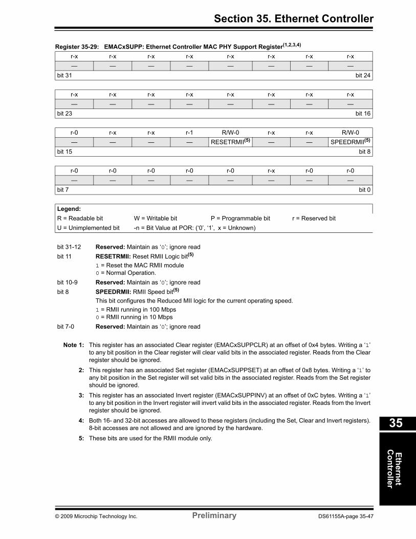
Section 35. Ethernet ControllerEthernet
Controller
35
Register 35-29: EMACxSUPP: Ethernet Controller MAC PHY Support Register(1,2,3,4)
r-x r-x r-x r-x r-x r-x r-x r-x— — — — — — — —
bit 31 bit 24
r-x r-x r-x r-x r-x r-x r-x r-x— — — — — — — —
bit 23 bit 16
r-0 r-x r-x r-1 R/W-0 r-x r-x R/W-0— — — — RESETRMII(5) — — SPEEDRMII(5)
bit 15 bit 8
r-0 r-0 r-0 r-0 r-0 r-x r-0 r-0— — — — — — — —
bit 7 bit 0
Legend:R = Readable bit W = Writable bit P = Programmable bit r = Reserved bitU = Unimplemented bit -n = Bit Value at POR: (‘0’, ‘1’, x = Unknown)
bit 31-12 Reserved: Maintain as ‘0’; ignore readbit 11 RESETRMII: Reset RMII Logic bit(5)
1 = Reset the MAC RMII module0 = Normal Operation.
bit 10-9 Reserved: Maintain as ‘0’; ignore readbit 8 SPEEDRMII: RMII Speed bit(5)
This bit configures the Reduced MII logic for the current operating speed.1 = RMII running in 100 Mbps0 = RMII running in 10 Mbps
bit 7-0 Reserved: Maintain as ‘0’; ignore read
Note 1: This register has an associated Clear register (EMACxSUPPCLR) at an offset of 0x4 bytes. Writing a ‘1’to any bit position in the Clear register will clear valid bits in the associated register. Reads from the Clearregister should be ignored.
2: This register has an associated Set register (EMACxSUPPSET) at an offset of 0x8 bytes. Writing a ‘1’ toany bit position in the Set register will set valid bits in the associated register. Reads from the Set registershould be ignored.
3: This register has an associated Invert register (EMACxSUPPINV) at an offset of 0xC bytes. Writing a ‘1’to any bit position in the Invert register will invert valid bits in the associated register. Reads from the Invertregister should be ignored.
4: Both 16- and 32-bit accesses are allowed to these registers (including the Set, Clear and Invert registers).8-bit accesses are not allowed and are ignored by the hardware.
5: These bits are used for the RMII module only.
© 2009 Microchip Technology Inc. Preliminary DS61155A-page 35-47
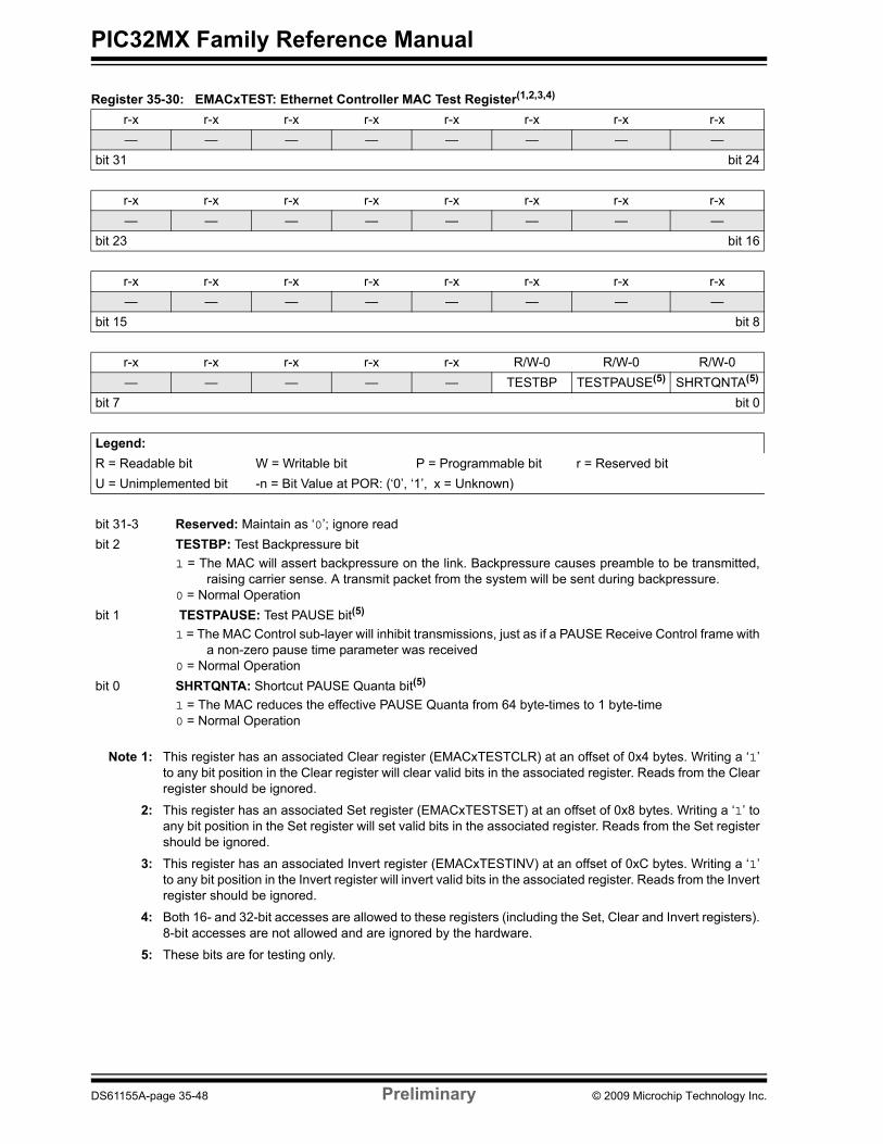
PIC32MX Family Reference Manual
Register 35-30: EMACxTEST: Ethernet Controller MAC Test Register(1,2,3,4)
r-x r-x r-x r-x r-x r-x r-x r-x— — — — — — — —
bit 31 bit 24
r-x r-x r-x r-x r-x r-x r-x r-x— — — — — — — —
bit 23 bit 16
r-x r-x r-x r-x r-x r-x r-x r-x— — — — — — — —
bit 15 bit 8
r-x r-x r-x r-x r-x R/W-0 R/W-0 R/W-0— — — — — TESTBP TESTPAUSE(5) SHRTQNTA(5)
bit 7 bit 0
Legend:R = Readable bit W = Writable bit P = Programmable bit r = Reserved bitU = Unimplemented bit -n = Bit Value at POR: (‘0’, ‘1’, x = Unknown)
bit 31-3 Reserved: Maintain as ‘0’; ignore readbit 2 TESTBP: Test Backpressure bit
1 = The MAC will assert backpressure on the link. Backpressure causes preamble to be transmitted,raising carrier sense. A transmit packet from the system will be sent during backpressure.
0 = Normal Operationbit 1 TESTPAUSE: Test PAUSE bit(5)
1 = The MAC Control sub-layer will inhibit transmissions, just as if a PAUSE Receive Control frame witha non-zero pause time parameter was received
0 = Normal Operationbit 0 SHRTQNTA: Shortcut PAUSE Quanta bit(5)
1 = The MAC reduces the effective PAUSE Quanta from 64 byte-times to 1 byte-time0 = Normal Operation
Note 1: This register has an associated Clear register (EMACxTESTCLR) at an offset of 0x4 bytes. Writing a ‘1’to any bit position in the Clear register will clear valid bits in the associated register. Reads from the Clearregister should be ignored.
2: This register has an associated Set register (EMACxTESTSET) at an offset of 0x8 bytes. Writing a ‘1’ toany bit position in the Set register will set valid bits in the associated register. Reads from the Set registershould be ignored.
3: This register has an associated Invert register (EMACxTESTINV) at an offset of 0xC bytes. Writing a ‘1’to any bit position in the Invert register will invert valid bits in the associated register. Reads from the Invertregister should be ignored.
4: Both 16- and 32-bit accesses are allowed to these registers (including the Set, Clear and Invert registers).8-bit accesses are not allowed and are ignored by the hardware.
5: These bits are for testing only.
DS61155A-page 35-48 Preliminary © 2009 Microchip Technology Inc.

Section 35. Ethernet ControllerEthernet
Controller
35
Register 35-31: EMACxMCFG: Ethernet Controller MAC MII Management Configuration Register(1,2,3,4)
r-x r-x r-x r-x r-x r-x r-x r-x— — — — — — — —
bit 31 bit 24
r-x r-x r-x r-x r-x r-x r-x r-x— — — — — — — —
bit 23 bit 16
R/W-0 r-x r-x r-x r-x r-x r-x r-xRESETMGMT — — — — — — —bit 15 bit 8
r-x r-x R/W-1 R/W-0 R/W-0 R/W-0 R/W-0 R/W-0— — CLKSEL<3:0>(5) NOPRE SCANINC
bit 7 bit 0
Legend:R = Readable bit W = Writable bit P = Programmable bit r = Reserved bitU = Unimplemented bit -n = Bit Value at POR: (‘0’, ‘1’, x = Unknown)
bit 31-16 Reserved: Maintain as ‘0’; ignore readbit 15 RESETMGMT: Test Reset MII Management bit
1 = Reset the MII Management module0 = Normal Operation
bit 14-6 Reserved: Maintain as ‘0’; ignore readbit 5-2 CLKSEL<3:0>: MII Management Clock Select 1 bits(5)
This field is used by the clock divide logic in creating the MII Management Clock (MDC), which IEEE802.3u defines to be no faster than 2.5 MHz. Some PHYs support clock rates up to 12.5 MHz.
bit 1 NOPRE: Suppress Preamble bit1 = The MII Management will perform read/write cycles without the 32-bit preamble field. Some PHYs
support suppressed preamble0 = Normal read/write cycles are performed
bit 0 SCANINC: Scan Increment bit1 = The MII Management module will perform read cycles across a range of PHYs. The read cycles
will start from address 1 through the value set in EMACxMADR<PHYADDR>0 = Continuous reads of the same PHY
Note 1: This register has an associated Clear register (EMACxMCFGCLR) at an offset of 0x4 bytes. Writing a ‘1’to any bit position in the Clear register will clear valid bits in the associated register. Reads from the Clearregister should be ignored.
2: This register has an associated Set register (EMACxMCFGSET) at an offset of 0x8 bytes. Writing a ‘1’ toany bit position in the Set register will set valid bits in the associated register. Reads from the Set registershould be ignored.
3: This register has an associated Invert register (EMACxMCFGINV) at an offset of 0xC bytes. Writing a ‘1’to any bit position in the Invert register will invert valid bits in the associated register. Reads from the Invertregister should be ignored.
4: Both 16- and 32-bit accesses are allowed to these registers (including the Set, Clear and Invert registers).8-bit accesses are not allowed and are ignored by the hardware.
5: Table 35-3 provides a description of the clock divider encoding.
© 2009 Microchip Technology Inc. Preliminary DS61155A-page 35-49

PIC32MX Family Reference Manual
Table 35-3: MIIM Clock Selection
MIIM Clock Select EMACxMCFG<5:2>
SCLK divided by 4 000x
SCLK divided by 6 0010
SCLK divided by 8 0011
SCLK divided by 10 0100
SCLK divided by 14 0101
SCLK divided by 20 0110
SCLK divided by 28 0111
SCLK divided by 40 1000
Undefined Any other combination
DS61155A-page 35-50 Preliminary © 2009 Microchip Technology Inc.

Section 35. Ethernet ControllerEthernet
Controller
35
Register 35-32: EMACxMCMD: Ethernet Controller MAC MII Management Command Register(1,2,3,4)
r-x r-x r-x r-x r-x r-x r-x r-x— — — — — — — —
bit 31 bit 24
r-x r-x r-x r-x r-x r-x r-x r-x— — — — — — — —
bit 23 bit 16
r-x r-x r-x r-x r-x r-x r-x r-x— — — — — — — —
bit 15 bit 8
r-x r-x r-x r-x r-x r-x R/W-0 R/W-0— — — — — — SCAN READ
bit 7 bit 0
Legend:R = Readable bit W = Writable bit P = Programmable bit r = Reserved bitU = Unimplemented bit -n = Bit Value at POR: (‘0’, ‘1’, x = Unknown)
bit 31-2 Reserved: Maintain as ‘0’; ignore readbit 1 SCAN: MII Management Scan Mode bit
1 = The MII Management module will perform read cycles continuously (for example, useful for moni-toring the Link Fail)
0 = Normal Operationbit 0 READ: MII Management Read Command bit
1 = The MII Management module will perform a single read cycle. The read data is returned in theEMACxMRDD register
0 = The MII Management module will perform a write cycle. The write data is taken from the EMACx-MWTD register
Note 1: This register has an associated Clear register (EMACxMCMDCLR) at an offset of 0x4 bytes. Writing a ‘1’to any bit position in the Clear register will clear valid bits in the associated register. Reads from the Clearregister should be ignored.
2: This register has an associated Set register (EMACxMCMDSET) at an offset of 0x8 bytes. Writing a ‘1’ toany bit position in the Set register will set valid bits in the associated register. Reads from the Set registershould be ignored.
3: This register has an associated Invert register (EMACxMCMDINV) at an offset of 0xC bytes. Writing a ‘1’to any bit position in the Invert register will invert valid bits in the associated register. Reads from the Invertregister should be ignored.
4: Both 16- and 32-bit accesses are allowed to these registers (including the Set, Clear and Invert registers).8-bit accesses are not allowed and are ignored by the hardware.
© 2009 Microchip Technology Inc. Preliminary DS61155A-page 35-51

PIC32MX Family Reference Manual
Register 35-33: EMACxMADR: Ethernet Controller MAC MII Management Address Register(1,2,3,4)
r-x r-x r-x r-x r-x r-x r-x r-x— — — — — — — —
bit 31 bit 24
r-x r-x r-x r-x r-x r-x r-x r-x— — — — — — — —
bit 23 bit 16
r-x r-x r-x R/W-0 R/W-0 R/W-0 R/W-0 R/W-1— — — PHYADDR<4:0>
bit 15 bit 8
r-x r-x r-x R/W-0 R/W-0 R/W-0 R/W-0 R/W-0— — — REGADDR<4:0>
bit 7 bit 0
Legend:R = Readable bit W = Writable bit P = Programmable bit r = Reserved bitU = Unimplemented bit -n = Bit Value at POR: (‘0’, ‘1’, x = Unknown)
bit 31-13 Reserved: Maintain as ’0’; ignore readbit 12-8 PHYADDR<4:0>: MII Management PHY Address bits
This field represents the 5-bit PHY Address field of Management cycles. Up to 31 PHYs can beaddressed (0 is reserved).
bit 7-5 Reserved: Maintain as ’0’; ignore readbit 4-0 REGADDR<4:0>: MII Management Register Address bits
This field represents the 5-bit Register Address field of Management cycles. Up to 32 registers can beaccessed.
Note 1: This register has an associated Clear register (EMACxMADRCLR) at an offset of 0x4 bytes. Writing a ‘1’to any bit position in the Clear register will clear valid bits in the associated register. Reads from the Clearregister should be ignored.
2: This register has an associated Set register (EMACxMADRSET) at an offset of 0x8 bytes. Writing a ‘1’ toany bit position in the Set register will set valid bits in the associated register. Reads from the Set registershould be ignored.
3: This register has an associated Invert register (EMACxMADRINV) at an offset of 0xC bytes. Writing a ‘1’to any bit position in the Invert register will invert valid bits in the associated register. Reads from the Invertregister should be ignored.
4: Both 16- and 32-bit accesses are allowed to these registers (including the Set, Clear and Invert registers).8-bit accesses are not allowed and are ignored by the hardware.
DS61155A-page 35-52 Preliminary © 2009 Microchip Technology Inc.

Section 35. Ethernet ControllerEthernet
Controller
35
Register 35-34: EMACxMWTD: Ethernet Controller MAC MII Management Write Data Register(1,2,3,4)
r-x r-x r-x r-x r-x r-x r-x r-x— — — — — — — —
bit 31 bit 24
r-x r-x r-x r-x r-x r-x r-x r-x— — — — — — — —
bit 23 bit 16
R/W-0 R/W-0 R/W-0 R/W-0 R/W-0 R/W-0 R/W-0 R/W-0MWTD<15:8>
bit 15 bit 8
R/W-0 R/W-0 R/W-0 R/W-0 R/W-0 R/W-0 R/W-0 R/W-0MWTD<7:0>
bit 7 bit 0
Legend:R = Readable bit W = Writable bit P = Programmable bit r = Reserved bitU = Unimplemented bit -n = Bit Value at POR: (‘0’, ‘1’, x = Unknown)
bit 31-16 Reserved: Maintain as ‘0’; ignore readbit 15-0 MWTD<15:0>: MII Management Write Data bits
When written, a MII Management write cycle is performed using the 16-bit data and the pre-configuredPHY and Register addresses from the EMACxMADR register.
Note 1: This register has an associated Clear register (EMACxMWTDCLR) at an offset of 0x4 bytes. Writing a ‘1’to any bit position in the Clear register will clear valid bits in the associated register. Reads from the Clearregister should be ignored.
2: This register has an associated Set register (EMACxMWTDSET) at an offset of 0x8 bytes. Writing a ‘1’ toany bit position in the Set register will set valid bits in the associated register. Reads from the Set registershould be ignored.
3: This register has an associated Invert register (EMACxMWTDINV) at an offset of 0xC bytes. Writing a ‘1’to any bit position in the Invert register will invert valid bits in the associated register. Reads from the Invertregister should be ignored.
4: Both 16- and 32-bit accesses are allowed to these registers (including the Set, Clear and Invert registers).8-bit accesses are not allowed and are ignored by the hardware.
© 2009 Microchip Technology Inc. Preliminary DS61155A-page 35-53
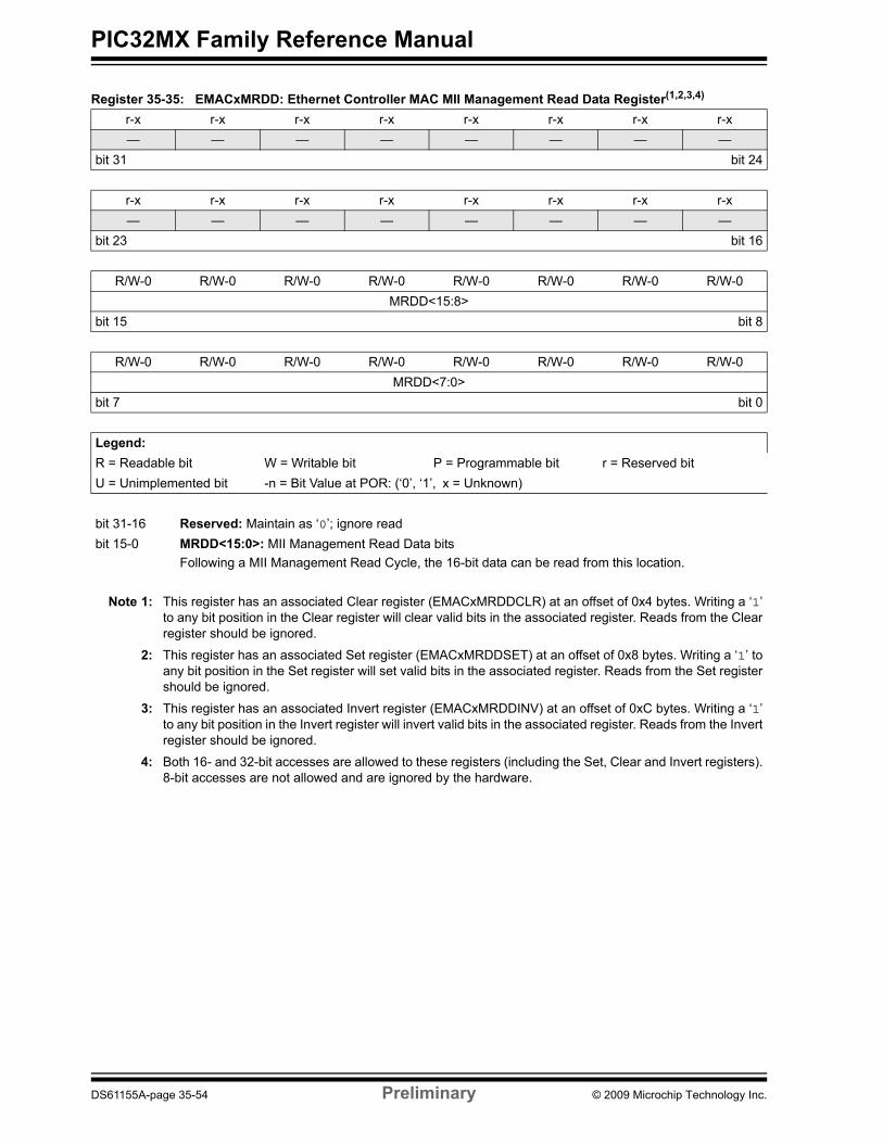
PIC32MX Family Reference Manual
Register 35-35: EMACxMRDD: Ethernet Controller MAC MII Management Read Data Register(1,2,3,4)
r-x r-x r-x r-x r-x r-x r-x r-x— — — — — — — —
bit 31 bit 24
r-x r-x r-x r-x r-x r-x r-x r-x— — — — — — — —
bit 23 bit 16
R/W-0 R/W-0 R/W-0 R/W-0 R/W-0 R/W-0 R/W-0 R/W-0MRDD<15:8>
bit 15 bit 8
R/W-0 R/W-0 R/W-0 R/W-0 R/W-0 R/W-0 R/W-0 R/W-0MRDD<7:0>
bit 7 bit 0
Legend:R = Readable bit W = Writable bit P = Programmable bit r = Reserved bitU = Unimplemented bit -n = Bit Value at POR: (‘0’, ‘1’, x = Unknown)
bit 31-16 Reserved: Maintain as ‘0’; ignore readbit 15-0 MRDD<15:0>: MII Management Read Data bits
Following a MII Management Read Cycle, the 16-bit data can be read from this location.
Note 1: This register has an associated Clear register (EMACxMRDDCLR) at an offset of 0x4 bytes. Writing a ‘1’to any bit position in the Clear register will clear valid bits in the associated register. Reads from the Clearregister should be ignored.
2: This register has an associated Set register (EMACxMRDDSET) at an offset of 0x8 bytes. Writing a ‘1’ toany bit position in the Set register will set valid bits in the associated register. Reads from the Set registershould be ignored.
3: This register has an associated Invert register (EMACxMRDDINV) at an offset of 0xC bytes. Writing a ‘1’to any bit position in the Invert register will invert valid bits in the associated register. Reads from the Invertregister should be ignored.
4: Both 16- and 32-bit accesses are allowed to these registers (including the Set, Clear and Invert registers).8-bit accesses are not allowed and are ignored by the hardware.
DS61155A-page 35-54 Preliminary © 2009 Microchip Technology Inc.

Section 35. Ethernet ControllerEthernet
Controller
35
Register 35-36: EMACxMIND: Ethernet Controller MAC MII Management Indicators Register(1,2,3,4)
r-x r-x r-x r-x r-x r-x r-x r-x— — — — — — — —
bit 31 bit 24
r-x r-x r-x r-x r-x r-x r-x r-x— — — — — — — —
bit 23 bit 16
r-x r-x r-x r-x r-x r-x r-x r-x— — — — — — — —
bit 15 bit 8
r-x r-x r-x r-x R/W-0 R/W-0 R/W-0 R/W-0— — — — LINKFAIL NOTVALID SCAN MIIMBUSY
bit 7 bit 0
Legend:R = Readable bit W = Writable bit P = Programmable bit r = Reserved bitU = Unimplemented bit -n = Bit Value at POR: (‘0’, ‘1’, x = Unknown)
bit 31-4 Reserved: Maintain as ‘0’; ignore readbit 3 LINKFAIL: Link Fail bit
When ‘1’ is returned - indicates link fail has occurred. This bit reflects the value last read from the PHYstatus register.
bit 2 NOTVALID: MII Management Read Data Not Valid bitWhen ‘1’ is returned - indicates an MII management read cycle has not completed and the Read Datais not yet valid.
bit 1 SCAN: MII Management Scanning bitWhen ‘1’ is returned - indicates a scan operation (continuous MII Management Read cycles) is inprogress.
bit 0 MIIMBUSY: MII Management Busy bitWhen ‘1’ is returned - indicates MII Management module is currently performing an MII ManagementRead or Write cycle.
Note 1: This register has an associated Clear register (EMACxMINDCLR) at an offset of 0x4 bytes. Writing a ‘1’to any bit position in the Clear register will clear valid bits in the associated register. Reads from the Clearregister should be ignored.
2: This register has an associated Set register (EMACxMINDSET) at an offset of 0x8 bytes. Writing a ‘1’ toany bit position in the Set register will set valid bits in the associated register. Reads from the Set registershould be ignored.
3: This register has an associated Invert register (EMACxMINDINV) at an offset of 0xC bytes. Writing a ‘1’ toany bit position in the Invert register will invert valid bits in the associated register. Reads from the Invertregister should be ignored.
4: Both 16- and 32-bit accesses are allowed to these registers (including the Set, Clear and Invert registers).8-bit accesses are not allowed and are ignored by the hardware.
© 2009 Microchip Technology Inc. Preliminary DS61155A-page 35-55

PIC32MX Family Reference Manual
Register 35-37: EMACxSA0: Ethernet Controller MAC Station Address 0 Register(1,2,3,4,5)
r-x r-x r-x r-x r-x r-x r-x r-x— — — — — — — —
bit 31 bit 24
r-x r-x r-x r-x r-x r-x r-x r-x— — — — — — — —
bit 23 bit 16
R/W-P R/W-P R/W-P R/W-P R/W-P R/W-P R/W-P R/W-PSTNADDR6<7:0>
bit 15 bit 8
R/W-P R/W-P R/W-P R/W-P R/W-P R/W-P R/W-P R/W-PSTNADDR5<7:0>
bit 7 bit 0
Legend:R = Readable bit W = Writable bit P = Programmable bit r = Reserved bitU = Unimplemented bit -n = Bit Value at POR: (‘0’, ‘1’, x = Unknown)
bit 31-16 Reserved: Maintain as ‘0’; ignore readbit 15-8 STNADDR6<7:0>: Station Address Octet 6 bits
This field holds the sixth transmitted octet of the station address.bit 7-0 STNADDR5<7:0>: Station Address Octet 5 bits
This field holds the fifth transmitted octet of the station address.
Note 1: This register has an associated Clear register (EMACxSA0CLR) at an offset of 0x4 bytes. Writing a ‘1’ toany bit position in the Clear register will clear valid bits in the associated register. Reads from the Clearregister should be ignored.
2: This register has an associated Set register (EMACxSA0SET) at an offset of 0x8 bytes. Writing a ‘1’ to anybit position in the Set register will set valid bits in the associated register. Reads from the Set registershould be ignored.
3: This register has an associated Invert register (EMACxSA0INV) at an offset of 0xC bytes. Writing a ‘1’ toany bit position in the Invert register will invert valid bits in the associated register. Reads from the Invertregister should be ignored.
4: Both 16- and 32-bit accesses are allowed to these registers (including the Set, Clear and Invert registers).8-bit accesses are not allowed and are ignored by the hardware.
5: This register is loaded at reset from the factory preprogrammed station address.
DS61155A-page 35-56 Preliminary © 2009 Microchip Technology Inc.

Section 35. Ethernet ControllerEthernet
Controller
35
Register 35-38: EMACxSA1: Ethernet Controller MAC Station Address 1 Register(1,2,3,4,5)
r-x r-x r-x r-x r-x r-x r-x r-x— — — — — — — —
bit 31 bit 24
r-x r-x r-x r-x r-x r-x r-x r-x— — — — — — — —
bit 23 bit 16
R/W-P R/W-P R/W-P R/W-P R/W-P R/W-P R/W-P R/W-PSTNADDR4<7:0>
bit 15 bit 8
R/W-P R/W-P R/W-P R/W-P R/W-P R/W-P R/W-P R/W-PSTNADDR3<7:0>
bit 7 bit 0
Legend:R = Readable bit W = Writable bit P = Programmable bit r = Reserved bitU = Unimplemented bit -n = Bit Value at POR: (‘0’, ‘1’, x = Unknown)
bit 31-16 Reserved: Maintain as ‘0’; ignore readbit 15-8 STNADDR4<7:0>: Station Address Octet 4 bits
This field holds the fourth transmitted octet of the station address.bit 7-0 STNADDR3<7:0>: Station Address Octet 3 bits
This field holds the third transmitted octet of the station address.
Note 1: This register has an associated Clear register (EMACxSA1CLR) at an offset of 0x4 bytes. Writing a ‘1’ toany bit position in the Clear register will clear valid bits in the associated register. Reads from the Clearregister should be ignored.
2: This register has an associated Set register (EMACxSA1SET) at an offset of 0x8 bytes. Writing a ‘1’ to anybit position in the Set register will set valid bits in the associated register. Reads from the Set registershould be ignored.
3: This register has an associated Invert register (EMACxSA1INV) at an offset of 0xC bytes. Writing a ‘1’ toany bit position in the Invert register will invert valid bits in the associated register. Reads from the Invertregister should be ignored.
4: Both 16- and 32-bit accesses are allowed to these registers (including the Set, Clear and Invert registers).8-bit accesses are not allowed and are ignored by the hardware.
5: This register is loaded at reset from the factory preprogrammed station address.
© 2009 Microchip Technology Inc. Preliminary DS61155A-page 35-57

PIC32MX Family Reference Manual
Register 35-39: EMACxSA2: Ethernet Controller MAC Station Address 2 Register(1,2,3,4,5)
r-x r-x r-x r-x r-x r-x r-x r-x— — — — — — — —
bit 31 bit 24
r-x r-x r-x r-x r-x r-x r-x r-x— — — — — — — —
bit 23 bit 16
R/W-P R/W-P R/W-P R/W-P R/W-P R/W-P R/W-P R/W-PSTNADDR2<7:0>
bit 15 bit 8
R/W-P R/W-P R/W-P R/W-P R/W-P R/W-P R/W-P R/W-PSTNADDR1<7:0>
bit 7 bit 0
Legend:R = Readable bit W = Writable bit P = Programmable bit r = Reserved bitU = Unimplemented bit -n = Bit Value at POR: (‘0’, ‘1’, x = Unknown)
bit 31-16 Reserved: Maintain as ‘0’; ignore readbit 15-8 STNADDR2<7:0>: Station Address Octet 2 bits
This field holds the second transmitted octet of the station address.bit 7-0 STNADDR1<7:0>: Station Address Octet 1 bits
This field holds the most significant (first transmitted) octet of the station address.
Note 1: This register has an associated Clear register (EMACxSA2CLR) at an offset of 0x4 bytes. Writing a ‘1’ toany bit position in the Clear register will clear valid bits in the associated register. Reads from the Clearregister should be ignored.
2: This register has an associated Set register (EMACxSA2SET) at an offset of 0x8 bytes. Writing a ‘1’ to anybit position in the Set register will set valid bits in the associated register. Reads from the Set registershould be ignored.
3: This register has an associated Invert register (EMACxSA2INV) at an offset of 0xC bytes. Writing a ‘1’ toany bit position in the Invert register will invert valid bits in the associated register. Reads from the Invertregister should be ignored.
4: Both 16- and 32-bit accesses are allowed to these registers (including the Set, Clear and Invert registers).8-bit accesses are not allowed and are ignored by the hardware.
5: This register is loaded at reset from the factory preprogrammed station address.
DS61155A-page 35-58 Preliminary © 2009 Microchip Technology Inc.

Section 35. Ethernet ControllerEthernet
Controller
35
35.4 OPERATIONThe Ethernet Controller provides the system modules needed to implement a 10/100 MbpsEthernet node using an external PHY chip. In order to offload the CPU from moving packet datato and from the module, two internal descriptor-based DMA engines are included in the controller.
The Ethernet Controller consists of the following sub-modules:
• 10/100 Megabit Media Access Controller (MAC): Implements the Media Access Control (MAC) sub-layer of the Data Link Layer and performs the CSMA/CD function contained in the ISO/IEC 8802-3 and the IEEE 802.3 specifications. It includes:- Media Independent Interface to connect to an external PHY- Reduced Media Independent Interface to connect to an external PHY- MII Management block that provides control/status connection to the external MII PHY- Performs the receive path flow control functions contained in IEEE 802.3 Annex 31B- Implements the MAC Transmit and MAC Receive interfaces that connect with the TX
and RX DMA engines• Flow Control (FC): Responsible for control of the transmission of PAUSE frames as defined
in IEEE 802.3 Annex 31B.• RX Filter (RXF): This block performs multiple filters on every receive packet to determine
whether each packet should be accepted or rejected.• TX DMA/TXBM Engine: The TX DMA engine and TX Buffer Management engine perform
data transfers from the packet buffers to the MAC Transmit Interface and also transfers the Transmit Status Vector (TSV) from the MAC to the packet buffers once the transmission is done. It operates using the TX Descriptor tables.
• RX DMA/RXBM Engine: The RX DMA engine and RX Buffer Management engine transfer receive packets and the Receive Status Vector (RSV) from the MAC to the packet buffers using the RX Descriptor tables.
35.4.1 Ethernet Frame OverviewIEEE 802.3-compliant Ethernet frames (packets) are between 64 and 1518 bytes long (Preambleand Start -of-Frame Delimiter not included). Frames containing less than 64 bytes are known as“runt” frames, while frames containing more than 1518 bytes are known as “huge” frames.
An Ethernet frame is made up of the following fields:
• Start-of-Stream/Preamble• Start-of-Frame Delimiter (SFD)• Destination MAC address (DA)• Source MAC address (SA)• Type/Length field• Data Payload• Optional Padding field• Frame Check Sequence (FCS)
Traffic on the actual physical cable is depicted in Figure 35-2. Please refer to the IEEE 802.3specification for detailed information about the Ethernet protocol.
35.4.1.1 START-OF-STREAM/PREAMBLE AND START-OF-FRAME DELIMITER
When transmitted on the Ethernet medium, The Start-of-Stream/Preamble and the SFD fields areappended to the beginning of an Ethernet frame automatically by the MAC.
When receiving, these fields are automatically stripped from the received frames so that thesefields are not written into the RX data buffers.
The software does not need to process/generate these fields.
35.4.1.2 DESTINATION MAC ADDRESS
A MAC address is a 6-octet number representing the physical address of the node(s) on anEthernet network. The destination address contains the MAC address of the device for which theframe is intended. There are different types of addresses in the Ethernet space. For example:
© 2009 Microchip Technology Inc. Preliminary DS61155A-page 35-59

PIC32MX Family Reference Manual
• Unicast Address: Designated for usage by the addressed node only. A Unicast address is an address where the Least Significant bit in the first byte of the address is zero (i.e., the first byte of the address is even). For example, “00 04 a3 00 00 01” is a Unicast address but “01 04 a3 00 00 01” is not.
• Multicast Address: Designated for use by a selected group of Ethernet nodes. A Multicast address is an address where the Least Significant bit in the first byte of this address is set (i.e., the byte is odd). For example, “01 04 a3 00 00 01” is a Multicast address. Note that the Multicast address, “FF-FF-FF-FF-FF-FF”, is reserved (Broadcast address) and is directed to all nodes on the network.
The Ethernet Controller incorporates a Receive Filter module that can be configured to accept ordiscard Unicast, Multicast and/or Broadcast frames. For details about the receive filters, refer toSection 35.4.8 “Receive Filtering Overview”.
35.4.1.3 SOURCE MAC ADDRESS
The source address is the 6-byte field MAC address of the node that transmitted the Ethernetframe. Every Ethernet device must have a globally unique MAC address. Each PIC32MXincluding an Ethernet Controller has a unique address, which is loaded into the MAC registerson power-up. This value can be used as is, or the registers may be reconfigured with a differentaddress at run time.
35.4.1.4 TYPE/LENGTH
This is a 2-byte field indicating the protocol to which the frame belongs. Applications usingstandards such as Internet Protocol (IP) or Address Resolution Protocol (ARP) should use thetype code specified in the appropriate standards document. Alternately, this field can be used asa length field when implementing proprietary networks. Typically, any value of 1500 (0x05DC) orsmaller is considered to be a length field and specifies the amount of non-padding data, whichfollows in the data field.
35.4.1.5 DATA
The data field typically consists of between 0 and 1500 bytes of payload data for each frame.PIC32MX devices are capable of transmitting and receiving frames larger than this when theHUGEFRM (EMACxCFG2<2>) bit is set. However, these larger frames that do not meet theIEEE 802.3 specifications will likely be dropped by most Ethernet nodes.
35.4.1.6 PADDING
The padding field is a variable length field appended to meet IEEE 802.3 specificationrequirements when transmitting small data payloads. The minimum payload for an Ethernetframe 46 bytes. Smaller frames must be padded to fill this space. For transmitted frames, thesoftware can instruct the Ethernet Controller to automatically generate the needed padding byusing the PADENABLE, VLANPAD and AUTOPAD bits (EMACxCFG2<5:7>). However, if theauto-padding is not enabled and the application does not provide appropriate padding, thePIC32MX device will not prevent the transmission of these “runt” frames. When receiving frames,PIC32MX devices accept and write all padding to the receive buffer. Frames shorter than therequired 64 bytes can optionally be filtered by the Runt Error Reject filter, described in Section35.4.8.4 “Runt Rejection Filter ”.
DS61155A-page 35-60 Preliminary © 2009 Microchip Technology Inc.
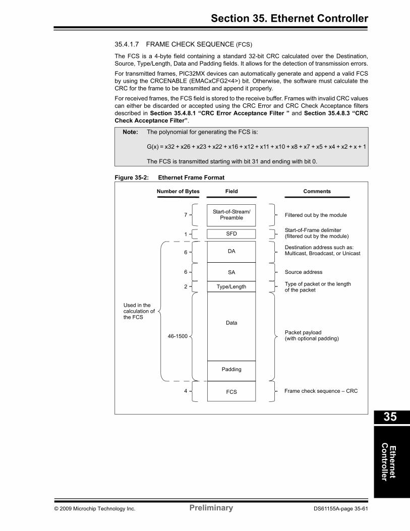
Section 35. Ethernet ControllerEthernet
Controller
35
35.4.1.7 FRAME CHECK SEQUENCE (FCS)
The FCS is a 4-byte field containing a standard 32-bit CRC calculated over the Destination,Source, Type/Length, Data and Padding fields. It allows for the detection of transmission errors.
For transmitted frames, PIC32MX devices can automatically generate and append a valid FCSby using the CRCENABLE (EMACxCFG2<4>) bit. Otherwise, the software must calculate theCRC for the frame to be transmitted and append it properly.
For received frames, the FCS field is stored to the receive buffer. Frames with invalid CRC valuescan either be discarded or accepted using the CRC Error and CRC Check Acceptance filtersdescribed in Section 35.4.8.1 “CRC Error Acceptance Filter ” and Section 35.4.8.3 “CRCCheck Acceptance Filter”.
Figure 35-2: Ethernet Frame Format
Note: The polynomial for generating the FCS is:
G(x) = x32 + x26 + x23 + x22 + x16 + x12 + x11 + x10 + x8 + x7 + x5 + x4 + x2 + x + 1
The FCS is transmitted starting with bit 31 and ending with bit 0.
Filtered out by the module
Start-of-Frame delimiter(filtered out by the module)
Destination address such as:Multicast, Broadcast, or Unicast
Source address
Type of packet or the length
Packet payload(with optional padding)
Frame check sequence – CRC
Start-of-Stream/Preamble
SFD
DA
SA
Type/Length
Data
Padding
FCS
7
1
6
6
2
46-1500
4
Used in thecalculation ofthe FCS
Number of Bytes Field Comments
of the packet
© 2009 Microchip Technology Inc. Preliminary DS61155A-page 35-61
PIC32MX Family Reference Manual
35.4.2 Basic Ethernet Controller OperationThe Ethernet Controller is enabled by setting the ON (ETHCON1<15>) bit in the ETHCON1register.
The Ethernet Controller is disabled by clearing the ON bit in the ETHCON1 register. This is thedefault state after any reset. If the Ethernet Controller is disabled, all of the I/O pins used for theMII/RMII and MIIM interfaces operate as port pins and are under the control of the respectivePORT latch bit and TRIS bit.
Disabling the controller resets the internal DMA state machines and all transmit and receiveoperations are aborted. The SFRs are still accessible and their values preserved.
Clearing the ON bit while the Ethernet Controller is active will abort all pending operations andreset the peripheral as defined above.
Re-enabling the ON bit will restart the Ethernet Controller in its clean reset state while preservingthe SFRs values.
35.4.3 MAC OverviewThe MAC sub-layer is part of the functionality described in the OSI model for the Data Link Layer.It defines a medium-independent facility, built on the medium-dependent physical facilityprovided by the Physical Layer, and under the access-layer-independent LLC sub-layer or otherMAC client. It is applicable to a general class of local area broadcast media suitable for use withthe Carrier Sense Multiple Access with Collision Detection (CSMA/CD).
The CSMA/CD MAC sub-layer provides services to the MAC client required for the transmissionand reception of frames. The CSMA/CD MAC sub-layer makes a best effort to acquire themedium and transfer a serial stream of bits to the Physical Layer. Although certain errors arereported to the client, error recovery is not provided by the MAC.
The following is a summary of the functional capabilities of the CSMA/CD MAC sub-layer asshown in Figure 35-3:
• For Frame Transmission:- Accepts data from the MAC client and constructs a frame- Presents a bit-serial data stream to the Physical Layer for transmission on the medium- In half-duplex mode, defers transmission of a bit-serial stream whenever the physical
medium is busy- It can append proper Frame Check Sequence (FCS) value to outgoing frames and
verifies full octet boundary alignment- Delays transmission of frame bit stream for specified inter-frame gap period- In half-duplex mode, halts transmission when collision is detected- In half-duplex mode, schedules retransmission after a collision until a specified retry
limit is reached- In half-duplex mode, enforces collision to ensure propagation throughout network by
sending jam message- Prepends preamble and Start Frame Delimiter and appends FCS to all frame Appends
PAD field for frames whose data length is less than a minimum value
Note 1: If the ‘ON’ bit is cleared during an active internal bus transaction, the controller willcomplete the current bus transaction before entering the disabled state. Once thecontroller is disabled, the TXBUSY (ETHSTAT<6>) and RXBUSY (ETHSTAT<5>)bits will reflect an inactive status.
2: Whenever the Ethernet Controller is reset via the ON bit, software should also resetthe external PHY via the MIIM registers. This insures the PHY is in a knowninitialized state. In addition, the MAC should also be soft reset via the EMACxCFG1register.
DS61155A-page 35-62 Preliminary © 2009 Microchip Technology Inc.

Section 35. Ethernet ControllerEthernet
Controller
35
• For Frame Reception:- Receives a bit-serial data stream from the Physical Layer- Presents the received frames to the MAC client (broadcast, multicast, unicast frames,
etc.)- Checks incoming frames for transmission errors by way of FCS and verifies octet
boundary alignment- Removes preamble, Start Frame Delimiter and PAD field (if necessary) from received
frames- Implements the MII Management block that provides control/status connection to the
external MII PHY
Figure 35-3: CSMA/CD Media Access Control Functions
The MAC is accessed using the following SFRs: EMACxCFG1, EMACxCFG2, EMACxIPGT,EMACxIPGR, EMACxCLRT, EMACxMAXF, EMACxSUPP, EMACxTEST and the EMACxSA0 toEMACxSA3 registers.
Note: For a detailed explanation of the MAC sub-layer functions and operation, pleasesee Clause 2, 3 and 4 of the IEEE 802.3 specification.
Physical Layer Signaling
ReceiveData Decoding
TransmitData Encoding
Access to Physical Interface
Receive MediaAccess Management
Transmit MediaAccess Management
TransmitData Encapsulation
ReceiveData Decapsulation
Access to MAC client
MAC Client Sub-Layer
© 2009 Microchip Technology Inc. Preliminary DS61155A-page 35-63

PIC32MX Family Reference Manual
35.4.4 Media Independent Interface (MII)The Media Independent Interface (MII) is a standard interconnection between the MAC and thePHY for communicating TX and RX frame data.This MII has the following important characteristics:• It is capable of supporting 10 Mbps and 100 Mbps rates for data transfer, and offers support
for management functions• It provides independent four bit wide transmit and receive data paths• It uses TTL signal levels, compatible with common digital CMOS processes• It provides full-duplex operationIn 10 Mbps mode, the MII runs at 2.5 MHz; in 100 Mbps mode it runs at 25 MHz. PHYs thatprovide MII are not required to support both data rates, and may support either one or both.Table 35-4 provides a list of the 18 Media Independent Interface signals.
Table 35-4: MII Signals
For detailed MII specifications, refer Clause 22 of the IEEE 802.3 specification.
Signal Name Width Type Description
TX_CLK 1 Input The transmit clock signal is a continuous clock that provides the timing reference for the transfer of the TX_EN, TXD and TX_ER signals from the MAC to the PHY. The TX_CLK frequency is a quarter of the nominal transmit data rate. A PHY operating at 100 Mbps must provide a TX_CLK frequency of 25 MHz, and a PHY operating at 10 Mbps must provide a TX_CLK frequency of 2.5 MHz.
RX_CLK 1 Input The receive clock signal is a continuous clock that provides the timing reference for the transfer of the RX_DV, RXD and RX_ER signals from the PHY to the MAC. RX_CLK has a frequency equal to a quarter of the data rate of the received signal.
TX_EN 1 Output The transmit enable signal indicates that the MAC is presenting nibbles on the MII for transmission. TX_EN transitions synchronously with respect to TX_CLK.
TXD<3:0> 4 Output The transmit data signals transition synchronously with respect to the TX_CLK.TX_ER 1 Output The transmit coding error signal is synchronous with respect to the TX_CLK. When
TX_ER is asserted for one or more TX_CLK periods while TX_EN is also asserted, the PHY will emit one or more symbols that are not part of the valid data or delimiter set somewhere in the frame being transmitted. This signal affects only 100 Mbps data transmission.
RX_DV 1 Input The receive data valid signal indicates that the PHY is presenting recovered and decoded nibbles on the RXD data lines. RX_DV is synchronous with RX_CLK. RX_DV remains asserted for the entire frame.
RXD<3:0> 4 Input The receive data signals represents the four data signals synchronous with respect to RX_CLK. For each RX_CLK period in which RX_DV is asserted, RXD<3:0> transfers four bits of recovered data from the PHY to the MAC.
RX_ER 1 Input The receive error signal is asserted to indicate to the MAC that a coding error (or any error that the PHY is capable of detecting) has occurred in the frame being transferred from the PHY to the MAC. RX_ER is synchronous with RX_CLK.
CRS 1 Input The carrier sense signal is asserted by the PHY when either the transmit or receive medium is non-idle. CRS will be de-asserted by the PHY when both the transmit and receive media are idle. The CRS remains asserted throughout the duration of a collision condition. It does not have to be synchronous with either the TX_CLK or the RX_CLK.
COL 1 Input The collision detected signal is asserted by the PHY upon detection of a collision on the medium, and remains asserted while the collision condition persists. It does not have to be synchronous with respect to either TX_CLK or RX_CLK.
MDC 1 Output The management data clock signal is part of the MII Management interface and is explained in Section 35.4.6 “Media Independent Interface Management (MIIM)”.
MDIO 1 Input/Output
The management data input/output signal is part of the MII Management interface and is explained in Section 35.4.6 “Media Independent Interface Management (MIIM)”.
DS61155A-page 35-64 Preliminary © 2009 Microchip Technology Inc.
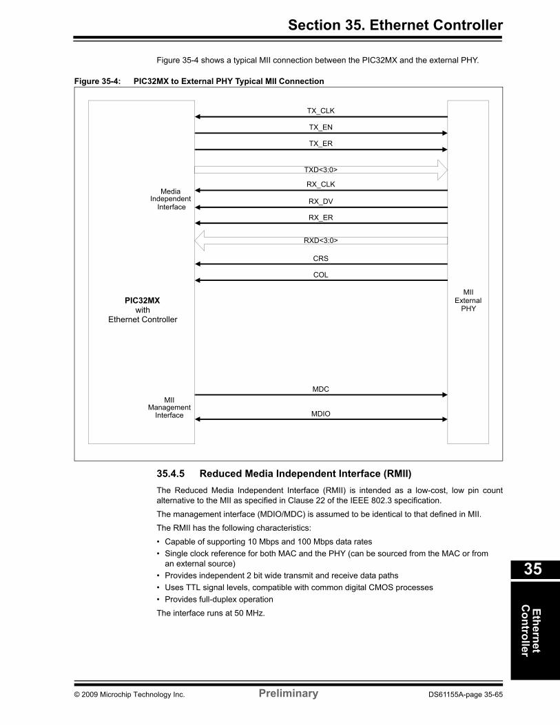
Section 35. Ethernet ControllerEthernet
Controller
35
Figure 35-4 shows a typical MII connection between the PIC32MX and the external PHY.
Figure 35-4: PIC32MX to External PHY Typical MII Connection
35.4.5 Reduced Media Independent Interface (RMII)The Reduced Media Independent Interface (RMII) is intended as a low-cost, low pin countalternative to the MII as specified in Clause 22 of the IEEE 802.3 specification.
The management interface (MDIO/MDC) is assumed to be identical to that defined in MII.
The RMII has the following characteristics:
• Capable of supporting 10 Mbps and 100 Mbps data rates• Single clock reference for both MAC and the PHY (can be sourced from the MAC or from
an external source)• Provides independent 2 bit wide transmit and receive data paths• Uses TTL signal levels, compatible with common digital CMOS processes• Provides full-duplex operation
The interface runs at 50 MHz.
PIC32MX with
Ethernet Controller
MIIExternal
PHY
MDC
MDIO
MIIManagement
Interface
TX_CLK
RX_CLK
TX_EN
TXD<3:0>
TX_ER
RX_DV
RXD<3:0>
RX_ER
CRS
COL
Media Independent
Interface
© 2009 Microchip Technology Inc. Preliminary DS61155A-page 35-65

PIC32MX Family Reference Manual
Table 35-5 provides a list of the 10 Reduced Media Independent Interface signals.
Table 35-5: RMII Signals
Refer the RMII Specification sponsored by the RMII Consortium for detailed specifications of theRMII.
Figure 35-5 shows a typical RMII connection between the PIC32MX and the external PHY.
Signal Name Width Type Description
REF_CLK 1 Input The reference clock signal is a continuous clock that provides the timing reference for CRS_DV, RXD<1:0>, TX_EN, TXD<1:0> and RX_ER. REF_CLK is a 50 MHz clock sig-nal sourced by the MAC or an external source. For PIC32MX devices, the REF_CLK is an external supplied clock signal.
CRS_DV 1 Input The carrier sense/receive data valid signal is asserted by the PHY when the receive medium is non-idle. CRS_DV is asserted asynchronously on detection of carrier. Loss of carrier results in the de-assertion of CRS_DV synchronous to the REF_CLK (only on nib-ble boundaries). The data on RXD<1:0> is considered valid once CRS_DV is asserted. Using the CRS_DV the MAC can accurately recover RX_DV and CRS.
RXD<1:0> 2 Input The receive data signals transition synchronously to REF_CLK. For each clock period in which CRS_DV is asserted, RXD transfers two bits of recovered data from the PHY.• RXD is ‘00’ to indicate the idle condition when CRS_DV is de-asserted. Since the
use of the PHY signal RX_ER is optional, in order to ensure the propagation of errors for the received signal, the RXD replaces the data in the decoded stream with ‘01’ so that the MAC CRC mechanism will reject the frame.
• In 100 Mbps RXD is synchronous to the REF_CLK.• In 10 Mbps the RXD is sampled every tenth cycle.
TX_EN 1 Output The transmit enable signal indicates that the MAC is presenting di-bits on TXD<1:0> for transmission. TX_EN is asserted with the first nibble of the preamble and remains asserted while all di-bits are transmitted. TX_EN is synchronous with respect to REF_CLK.
TXD<1:0> 2 Output The transmit data signal is transmits data to the PHY when TX_EN is asserted. The TXD data lines transition synchronously with respect to REF_CLK. TXD uses the value of ‘00’ to signal idle when the TX_EN is de-asserted.• In 100 Mbps mode, TXD provides valid data for each REF_CLK period while TX_EN
is asserted.• In 10 Mbps mode since the REF_CLK frequency is 10 times the data rate the value
on TXD is sampled every tenth cycle.RX_ER 1 Input The receive error signal is asserted for one or more REF_CLK periods to indicate that an
error was detected somewhere in the frame presently being transferred from the PHY. RX_ER is synchronous with respect to REF_CLK.
MDC 1 Output The management data clock signal is part of the MII Management interface and is explained in Section 35.4.6 “Media Independent Interface Management (MIIM)”.
MDIO 1 Input/Output
The management data input/output signal is part of the MII Management interface and is explained in Section 35.4.6 “Media Independent Interface Management (MIIM)”.
DS61155A-page 35-66 Preliminary © 2009 Microchip Technology Inc.

Section 35. Ethernet ControllerEthernet
Controller
35
Figure 35-5: PIC32MX to External PHY Typical RMII Connection
PIC32MX with
Ethernet Controller
RMIIExternal
PHY
MDC
MDIO
RMIIManagement
Interface
REF_CLK
TX_EN
TXD<1:0>
RXD<1:0>
RX_ER
CRS_DV
ReducedMedia
Independent Interface
ExternalClock
Source
© 2009 Microchip Technology Inc. Preliminary DS61155A-page 35-67
PIC32MX Family Reference Manual
35.4.6 Media Independent Interface Management (MIIM)The MII Management (MIIM) module provides a serial communication link between the PIC32MXhost and an external MII PHY device. The external serial communications link operates inaccordance with IEEE 802.3 Clause 22 Standards.
The MIIM input/output signals are:
• Management Data Clock (MDC) – MDC is sourced by the MAC to the PHY as the timing reference for transfer of information on the MDIO signal.
• Management Data Input/Output (MDIO) – MDIO is a bidirectional signal between the PHY and the MAC. It is used to transfer control information and status between the PHY and the MAC. Control information is driven by the MAC synchronously with respect to MDC and is sampled synchronously by the PHY. Status information is driven by the PHY synchronously with respect to MDC and is sampled synchronously by the MAC.
The communication over the MIIM link takes place in frames. Frames transmitted on the MIIManagement Interface have the following structure (see Table 35-6):
• Preamble: At the beginning of each transaction, the MAC sends a sequence of 32 logic one bits on MDIO to provide the PHY with a synchronization pattern.
• Start-of-frame: The start-of-frame is indicated by a <01> pattern.• Operation code: <10> for a read transaction, <01> for a write transaction.• PHY Address: Five bits, allowing 32 unique PHY addresses. A PHY will always respond to
transactions with address zero.• Register Address: Five bits, allowing 32 individual registers to be addressed within each
PHY.• Turnaround: A 2-bit-time spacing between the Register Address field and the Data field of a
management frame to avoid contention during a read transaction.• Data: This 16-bit field carries the data to/from the addressed PHY register.
Table 35-6: MIIM Frame Format
As indicated above, the size of a MIIM frame is 64 bits. However, the MIIM module may beconfigured to suppress the preamble portion of the MII Management serial stream using theNOPRE (EMACxMCFG<1>) bit when the PHY supports a suppressed preamble operation.
Refer the Clause 22 Standard in the IEEE 802.3 specification for MIIM details.
Note: The IDLE condition on MDIO is a high-impedance state.
OperationManagement Frame Fields
PRE ST OPCODE PHYAD REGAD TA DATA IDLE
READ 1….1 01 10 a0…a4 r0…r4 Z0 d0….d15 ZWRITE 1….1 01 01 a0…a4 r0…r4 10 d0….d15 Z
DS61155A-page 35-68 Preliminary © 2009 Microchip Technology Inc.

Section 35. Ethernet ControllerEthernet
Controller
35
35.4.6.1 EXTERNAL PHY REGISTER ACCESS
The PHY registers provide configuration and control of the PHY module, as well as statusinformation about its operation. Unlike the on-chip SFRs, the PHY registers are not directlyaccessible through the SFR control interface. Instead, access is accomplished through a specialset of MAC control registers that implement the Media Independent Interface Management.These control registers are referred to as the MIIM registers. The PHY registers are accessedthrough the MIIM interface of the MAC. To do this, the MII Management Command, Address andData registers in the MAC must be used.
The registers that control access to the PHY registers are listed in the Ethernet Control RegisterSummary (Table 35-1) and include the following registers:
• EMACxMCFG: Ethernet Controller MAC MII Management Configuration Register• EMACxMCMD: Ethernet Controller MAC MII Management Command Register• EMACxMADR: Ethernet Controller MAC MII Management Address Register• EMACxMWTD: Ethernet Controller MAC MII Management Write Data Register• EMACxMRDD: Ethernet Controller MAC MII Management Read Data Register• EMACxMIND: Ethernet Controller MAC MII Management Indicators Register
35.4.6.2 INITIALIZING THE MII MANAGEMENT MODULE
In order for the MAC MIIM module to create the proper interface clock (MDC) frequency the clockspeed needs to be configured. The MIIM module uses the SCLK as an input clock.
Use the CLKSEL (EMACxMCFG<2:5>) bits to select the divider for creating the MDC clocksignal, which the IEEE 802.3 specification defines to be no faster than 2.5 MHz. However, somePHYs support clock rates up to 12.5 MHz.
35.4.6.3 READING A PHY REGISTER
When a PHY register is read via the MAC, the entire 16 bits are obtained.
To read from a PHY register, do the following:
1. Write the address of the PHY and of the PHY register to read from into the EMACxMADRregister.
2. Set the READ (EMACxMCMD<0>) bit. The read operation begins and the MIIMBUSY(EMACxMIND<0>) bit will be set after three SCLK periods (this is due to the internalpipeline of the MIIM interface).
3. Poll the MIIMBUSY bit to be certain that the operation is complete (the operation time isthe one needed to transfer a full MIIM frame). While busy, the software should not startany MII scan operations or write to the EMACxMWTD register. When the MAC hasobtained the register contents, the MIIMBUSY bit will clear itself.
4. Clear the READ (EMACxMCMD<0>) bit.5. Read the desired data from the EMACxMRDD register.
Note: All PHY chip registers are treated as 16 bits in width. Writes to unimplemented loca-tions are ignored and any attempts to read these locations will return ‘0’. Allreserved locations should be written as ‘0’; their contents should be ignored whenread. Refer the vendor-specific PHY data sheet for register access details.
© 2009 Microchip Technology Inc. Preliminary DS61155A-page 35-69

PIC32MX Family Reference Manual
35.4.6.4 WRITING A PHY REGISTER
When a PHY register is written to, all 16 bits are written at once; selective bit writes are notimplemented. If it is necessary to reprogram only select bits in the register, the software must firstread the PHY register, modify the resulting data, and then write the data back to the PHY register.
To write to a PHY register, do the following:
1. Write the address of the PHY and of the PHY register to read from into the EMACxMADRregister.
2. Write the 16 bits of data to be written into the EMACxMWTD register. Writing to thisregister automatically begins the MIIM transaction, which causes the MIIMBUSY(EMACxMIND<0>) bit to be set after three SCLK periods (this is due to the internalpipeline of the MIIM interface).
3. Poll the MIIMBUSY bit until it is cleared, which indicates the write has completed. 4. The PHY register will be written after the MIIM operation completes, which takes a MIIM
frame time. When the write operation has completed, the MIIMBUSY bit will clear itself.The software should not start any MII scan or read operations while busy.
35.4.6.5 SCANNING A PHY REGISTER
The MAC can be configured to perform automatic back-to-back read operations on a PHYregister. This can significantly reduce the software complexity when periodic status informationupdates are desired.
To perform the scan operation, do the following:1. Write the address of the PHY and the address of the PHY register to be read from into the
EMACxMADR register.2. Set the SCAN (EMACxMCMD<1>) bit. The scan operation begins and the MIIMBUSY
(EMACxMIND<0>) bit is set.3. The first read operation will complete after the first MIIM frame is transferred. Subsequent
reads will be done at the same interval until the operation is cancelled. The NOTVALID(EMACxMIND<2>) bit may be polled to determine when the first read operation iscomplete. Read the scanned register data from the EMACxMRDD register.
4. After setting the SCAN bit, the EMACxMRDD register will automatically be updated everyMIIM frame interval. There is no status information which can be used to determine whenthe EMACxMRDD register is updated.
5. When the MIIM scan operation is in progress, the software must not attempt to write toEMACxMWTD or start a read operation.
6. The MIIM scan operation can be cancelled by clearing the SCAN (EMACxMCMD<1>) bitand then polling the MIIMBUSY bit. New operations may be started after the MIIMBUSYbit is cleared.
Example 35-1 provides example code for a MIIM initialization and PHY register read, write andscan.
DS61155A-page 35-70 Preliminary © 2009 Microchip Technology Inc.

Section 35. Ethernet ControllerEthernet
Controller
35
Example 35-1: MIIM Initialization and PHY Access// Assume we're running at 80 MHz and we're working with a PHY that supports a maximum// 2.5 MHz MIIM frequency
#include <p32xxxx.h>#define PHY_ADDRESS 0x1f // the address of the PHY
EMACxMCFG=0x00008000; // issue resetEMACxMCFG=0; // clear resetEMACxMCFG=(0x8)<<2; // program the MIIM clock, divide by 40
// read the basic status PHY register: 1unsigned int phyRegVal;
while(EMACxMIND&0x1); // wait not busyEMACxMADR=0x1|((PHY_ADDRESS)<<8); // set the PHY and register addressEMACxMCMD=1; // issue the read order__asm__ __volatile__ (“nop; nop; nop;”); // wait busy to be setwhile(EMACxMIND&0x1); // wait op completeEMACxMCMD=0; // clear command registerphyRegVal=EMACxMRDD; // read the selected register
// write the basic control PHY register: 0while(EMACxMIND&0x1); // wait in case of some previous operationEMACxMADR=0x0|((PHY_ADDRESS)<<8); // set the PHY and register addressEMACxMWT=0x8000; // issue the write order (PHY reset)__asm__ __volatile__ (“nop; nop; nop;”); // wait busy to be setwhile(EMACxMIND&0x1); // wait write complete
// Make sure data has been written
// Perform a scan of the status PHY register: 1// Start the scanwhile(EMACxMIND&0x1); // wait in case of some previous operationEMACxMADR=0x1|((PHY_ADDRESS)<<8); // set the PHY and register addressEMACxMCMD=0x2; // issue the scan order
// Read the status register
// Note that the read can occur now at any time// without previously selecting the read operation and the registerwhile(EMACxMIND&0x4); // wait data validphyRegVal=EMACxMRDD; // read the scanned register
© 2009 Microchip Technology Inc. Preliminary DS61155A-page 35-71

PIC32MX Family Reference Manual
35.4.7 Flow Control OverviewEthernet flow control consists of the ability to send and receive PAUSE frames, which cause thereceiving node to stop transmitting for a specific amount of time.
On the transmit side, the Flow Control (FC) block handles the hardware handshaking betweenthe MAC and the CPU when the transmit flow control is enabled. Flow control for the receivedpackets is part of the MAC functionality.
The PIC32MX MAC supports both Symmetric PAUSE and Asymmetric PAUSE as described inClause 28, Table 28B-2 and Clause 31 and Annex 31B of the IEEE 802.3 Standard.
The FC block supports two modes of operation: manual and automatic. In addition, the mode oftransmission (Full-Duplex or Half-Duplex) programmed into the MAC registers, is used by the FCblock.
Before software can throttle down incoming packets, it must enable flow control. The flow controlmechanism operates differently between Full-Duplex and Half-Duplex modes.
35.4.7.1 FULL-DUPLEX
On the transmit side the MAC will send a PAUSE control frame with a PAUSE Timer value. Thereceiving MAC decodes the control frame, extracts the PAUSE Timer value and stallstransmission for the designated time. Note that this does not imply the transmitting device willpause immediately. There is latency in the activation of the pause mechanism. If flow control isto be deactivated before the PAUSE Timer value expires, another PAUSE frame can be sent thatencodes a value of 0x0000 for the PAUSE Timer value.
Looking at the operation from the receiving end, if another device transmits a PAUSE frame andthe MAC receives a PAUSE frame, then the transmit operation will be inhibited until the PAUSETimer expires or the other device cancels the request for pause frames.
35.4.7.2 HALF-DUPLEX
Half-duplex flow control is similar in operation. When the software enables the flow control theFC block requests the MAC to apply backpressure. The MAC will continue sending a preamblepattern on the transmit line to prevent any other device from gaining control of the bus. This willcontinue until flow control is disabled.
35.4.7.3 MANUAL FLOW CONTROL
The manual flow control is enabled via the MANFC (ETHCON1<4>) control bit.When manual flow control is enabled, the MAC sends PAUSE control frames using the PTV(ETHCON1<31:16>) value. When transmit flow control is disabled, the MAC will send anotherPAUSE frame that encodes a value of 0x0000 for the PAUSE Timer value in order to disable flowcontrol.
Note: The software should not change the Full-Duplex or Half-duplex mode of operationwhile the transmit logic is in the middle of transmitting a package.
Note: A PAUSE frame includes the period of pause time being requested, in the range of0 through 65535. The pause time is measured in units of pause “quanta”, whereeach unit is equal to 512 bit times.
DS61155A-page 35-72 Preliminary © 2009 Microchip Technology Inc.
Section 35. Ethernet ControllerEthernet
Controller
35
35.4.7.4 AUTOMATIC FLOW CONTROL
The automatic flow control is enabled via the AUTOFC (ETHCON1<7>) control bit. Whenautomatic flow control is enabled, PAUSE control frames are sent by hardware based on thecurrent value of the BUFCNT (ETHSTAT<23:16>) bit as follows:
• When BUFCNT reaches the value specified by the RXFWM (ETHRXWM<23:16>) bit, a PAUSE frame is automatically sent every 512/2 * PTV (ETHCON1<31:16>) transmit clock cycles.
• When BUFCNT reaches the value specified by the RXEWM (ETHRXWM<7:0>), a PAUSE frame with the PAUSE Timer Value set to 0x0000 is sent.
Note that the BUFCNT value is updated only on a packet boundary; therefore, all automatic flowcontrol changes occur on packet boundaries.
When automatic flow control is enabled, it has the highest priority for setting and clearing flowcontrol operations. Therefore, it is not recommended to mix automatic and manual flow control.
The sequence of steps needed to manually transmit a PAUSE frame are:
1. In the initialization sequence software sets the PAUSE value by writing the PTV value(ETHCON1<31:16>).
2. Software writes the MANFC bit (ETHCON1<4>) to manually start the transmission of aPAUSE frame.
3. The FC block will request the MAC to send a PAUSE frame.4. The MAC will assemble the complete Flow Control frame, as follows:
a) Preambleb) Start Frame Delimiter (SFD)c) Destination Address = 01-80-c2-00-00-01 (Special PAUSE multi-cast address) d) Source Address = Station Address from EMACxSA0-EMACxSA3 registerse) Length = 0x8088 (Control Frame)f) Payload:
• Opcode (2 bytes) = 0x0001• PAUSE Value (2 bytes) = PTV
g) Padh) FCS
Example 35-2: Using Manual Flow Control Code
Note 1: The transmit clock cycle is 10 MHz or 100 MHz depending on the current MACspeed selection: 10 Mbps or 100 Mbps.
2: Software must insure that the flow control watermark values allow PAUSE framesto be sent when the amount of free space allocated by the free RX descriptorsdrops below two times maximum Ethernet frame size (i.e., 1536 *2). This will insurethere is no receive overflow conditions.
3: The PTV value may only be changed when the operation is not enabledETHCON1<15> = 0.
// Note: Setting the new PTV value should be done only when the // peripheral is not enabled#include <p32xxxx.h>ETHCON1CLR=0xffff0000; // clear PTVETHCON1SET=(ptvVal)<<16; // set the new PTV value
/*....*/ETHCON1SET=0x10; // turn on the Manual Flow Control
// at this moment PAUSE Frames are being sent// or backpressure is applied
// do some other things// manage/retrieve all the received packets so far// ...// ...
ETHCON1CLR=0x10; // disable the Manual Flow Control
© 2009 Microchip Technology Inc. Preliminary DS61155A-page 35-73
PIC32MX Family Reference Manual
35.4.8 Receive Filtering OverviewThe Receive Filter (RXF) block examines all incoming receive packets and accepts or rejects thepacket, based on user-selectable filters. The following RX filters are supported:
• CRC Error Acceptance Filter controlled by CRCERREN (ETHRXFC<7>)• Runt Error Acceptance Filter controlled by RUNTERREN (ETHRXFC<5>)• CRC Check Rejection Filter controlled by CRCOKEN (ETHRXFC<6>)• Runt Rejection Filter controlled by RUNTEN (ETHRXFC<4>)• Unicast Acceptance Filter controlled by UCEN (ETHRXFC<3>)• Not Me Unicast Acceptance Filter controlled by NOTMEEN (ETHRXFC<2>)• Multicast Acceptance Filter controlled by MCEN (ETHRXFC<1>)• Broadcast Acceptance Filter controlled by BCEN (ETHRXFC<0>)• Hash Table Acceptance Filter controlled by HTEN (ETHRXFC<15>)• Magic Packet Acceptance Filter controlled by MPEN (ETHRXFC<14>)• Pattern Match Acceptance Filter with logical inversion controlled by PMMODE
(ETHRXFC<8-11>) and NOTPM (ETHRXFC<12>)
The order of the filters above specifies the priority of the filter from highest-to-lowest, such that ifa filter is enabled and accepts or rejects a packet, all lower priority filters will have no effect.
For example, if the Runt Error Acceptance Filter is enabled and a packet of less than 64 bytes isreceived, it will always be accepted, even if the CRC check fails.
If a received packet is not explicitly accepted or discarded by an enabled filter, the packet will bediscarded by default.
Due to the internal design of the RX Filter, the final accept versus abort decision for an Ethernetframe is made at the end of the frame.
When a packet is received, the Receive Status Vector (RSV) for each receive packet containsinformation about which filters matched the corresponding RX packet, regardless of whetherthese filters were active at the time. This provides extra “status” information about the packet thatmay be used to filter packets in software. For example, in Promiscuous mode, the Magic Packetfilter RSV bit may be used to quickly identify a Magic Packet without the need to examine theframe contents. Please refer to the Ethernet Descriptor Table Format (Linked List, NPV = 1)(Table 35-9) for more information on the RSV.
All filter settings are done using the ETHRXFC register.
Due to synchronization in the RXF block, the following registers should not be changed while theON bit (ETHCON1<15>) is set:
• ETHRXFC: Ethernet Controller Receive Filter Configuration Register• ETHHT0: Ethernet Controller Hash Table 0 Register• ETHHT1: Ethernet Controller Hash Table 1 Register• ETHPMO: Ethernet Controller Pattern Match Offset Register• ETHPMCS: Ethernet Controller Pattern Match Checksum Register• ETHPMM0: Ethernet Controller Pattern Match Mask 0 Register• ETHPMM1: Ethernet Controller Pattern Match Mask 1 Register• EMACxSA0: Ethernet Controller MAC Station Address 0 Register• EMACxSA1: Ethernet Controller MAC Station Address 1 Register• EMACxSA2: Ethernet Controller MAC Station Address 2 Register
To change one or more of these registers/register bits, you must first clear the ON(ETHCON1<15>) bit.
Following are short summaries of each receive filter.
Note: Each filter is either an Acceptance filter or a Rejection filter. Acceptance filters forcethe acceptance of a packet, while rejection filters force the rejection of a packet.
DS61155A-page 35-74 Preliminary © 2009 Microchip Technology Inc.

Section 35. Ethernet ControllerEthernet
Controller
35
35.4.8.1 CRC ERROR ACCEPTANCE FILTER
This filter is used to explicitly accept packets that fail the CRC check. If enabled, all packets thatfail the CRC check are accepted, regardless of whether the CRC Check Filter is enabled or not.
35.4.8.2 RUNT ERROR ACCEPTANCE FILTER
This filter is used to explicitly accept packets that fail the Runt check. If enabled, all packets thatfail the Runt check are accepted, regardless of whether the Runt Filter is enabled or not.
35.4.8.3 CRC CHECK ACCEPTANCE FILTER
If enabled, results of the MAC CRC check will be examined and used to filter the packet. If thisfilter is enabled and fails, the packet will be aborted. Conversely, if CRC checking is not enabled,the received packet’s CRC is ignored and is not used as an acceptance requirement for thepacket.
35.4.8.4 RUNT REJECTION FILTER
The Runt Filter allows filtering on the size of the received packet (Destination Address, SourceAddress, Length/Type, Payload and FCS). When the Runt Rejection Filter is enabled packetssmaller than 64 bytes will be rejected.
35.4.8.5 CAST ACCEPTANCE FILTER
The packet is filtered by its cast, with support for the following:
• Unicast: Accepts any packet that is of type Unicast and whose Destination Address matches the Station Address
• Not Me Unicast: Accepts any packet that is of type Unicast and whose Destination Address does not match the Station Address
• Broadcast: Accepts any packet that is of type Broadcast• Multicast: Accepts any packet that is of type Multicast
A receive packet may be accepted (depending on the other filters) if any of the active cast filtersaccept the packet. Enabling both the Unicast and Broadcast filters, for example, would alloweither type of packet to be received.
To accept all incoming packets (Promiscuous mode), simply enable the UCEN, NOTMEEN,MCEN and BCEN filters, and disable all other filters.
35.4.8.6 HASH TABLE ACCEPTANCE FILTER
When enabled, the Hash Table filter accepts received packets based on their destinationaddress, with up to 64 different addresses allowed. This is done by using the Destination AddressCRC output from the MAC as a lookup key in a user-defined Hash Table.
First, the CRC value is calculated on the received packet Destination Address field. Bits <28:23>of this value are then used as an index into a 64-bit user-programmable table (ETHHT0,ETHHT1) containing single-bit accept (‘1’) or ignore (‘0’) values. For example, if the calculatedCRC has a value of 05h, the value in bit 5 of the 64-bit HT register table is examined. If that entryis a logical ‘1’, the packet is accepted; otherwise, the filter results are not taken into account whendeciding whether to accept the packet or not.
Note that the Destination Address CRC output used by this filter corresponds to bits <28:23> ofthe uncomplemented 32-bit CRC over the Destination Address of the RX packet.
35.4.8.7 MAGIC PACKET ACCEPTANCE FILTER
The Magic Packet filter scans the received packet for a predetermined pattern to accept thepacket.
A Magic Packet is defined by the following: the Data field contains a synchronization pattern ofsix 0xFFh bytes followed by the Destination Station Address repeated sixteen times.
The data packet may contain additional payload besides the Magic Packet pattern.
© 2009 Microchip Technology Inc. Preliminary DS61155A-page 35-75

PIC32MX Family Reference Manual
Figure 35-6: Sample Magic Packet™ Format
35.4.8.8 PATTERN MATCH ACCEPTANCE FILTER
When enabled, the Pattern Match Acceptance filter accepts packets that match a certain pattern.The match is accomplished by generating a Checksum of the selected bytes in a 64-byte window.
If the calculated checksum is equal or not equal to the ETHPMCS register, as specified by theNOTPM (ETXRXFC<12>) bit, and all conditions associated with PMMODE (ETHRXFC<8-11>)are met, the packet is accepted. Otherwise, the packet is aborted.
The 64-byte window is programmed using the PMO value (ETHPMO<15:0>) so that the start ofthe window can be anywhere from 0 to 65536 bytes. However, if the 64-byte window extendspast the end of the packet, the pattern match filter aborts the packet.
The Pattern Match Mask bits PMM<63:0> (ETHPMM0<31:0>, ETHPMM1<31:0>) are used toselect whether or not the given byte in the 64-byte window is used in the computation of theChecksum. If the Pattern Match Mask bit (PMM<n>) in the Ethernet Pattern Match Maskregisters (ETHPMM0, ETHPMM1) is set, the respective byte is used in the Checksumcomputation (where n = 0, 1, 2,..., 62, 63 and n = 0 points to the first byte after the offset value).
The Checksum algorithm is the same as the TCP/IP checksum calculation. Note that thealgorithm requires that the calculation uses a 16-bit word length. This means that the data seriesused for the calculation will have a zero byte of padding for the last byte if an odd number of bytesare to be matched. Also, the Checksum value is initialized to 0x00000000h before the calculationis started. Figure 35-7 shows an example of Checksum calculation.
SA
FCS
DA
Type/Length
Data
11 22 33 44 55 66
00 FE
09 0A 0B 0C 0D 0E
ReceivedData Field
77 88 99 AA BB CC
EF 54 32 10
FF FF FF FF FF 00
FF FF FF FF FF FF
11 22 33 44 55 66
11 22 33 44 55 66
11 22 33 44 55 66
11 22 33 44 55 66
11 22 33 44 55 66
11 22 33 44 55 66
11 22 33 44 55 66
11 22 33 44 55 66
11 22 33 44 55 66
11 22 33 44 55 66
11 22 33 44 55 66
11 22 33 44 55 66
11 22 33 44 55 66
11 22 33 44 55 66
11 22 33 44 55 66
11 22 33 44 55 66
19 1A 1B 1C 1D 1E
Data
Sync pattern
Sixteen repeats ofthe Station Address
DS61155A-page 35-76 Preliminary © 2009 Microchip Technology Inc.

Section 35. Ethernet ControllerEthernet
Controller
35
Figure 35-7: Checksum Calculation
Figure 35-8 shows a sample Pattern Match format.
Figure 35-8: Sample Pattern Match Format
12 00 AC 23 92 55 00 00 FE AA FF FF 34 12 CD AB <-- Data Packet (hex) 0 1 2 3 4 5 6 7 8 9 10 11 12 13 14 15 <-- Byte Number
Step 1: Add words of data packet:
1200h + AC23h + 9255h + 0000h + FEAAh + FFFFh + 3412h + CDABh = 450DEh
Step 2a: Add high word with low word of checksum_reg:50DEh + 0004h = 50E2h
checksum_reg[31:0] = 0x0004_50DE
checksum_reg[31:0] = 0000_50E2h
Step 3: NOT(000050E2h) = FFFFAF1Dh
checksum_reg[31:0] = 0000_50E2houtput dma_checksum_val[15:0] = AF1Dh
Note 1: The calculation shown above assumes an initial seed of 0000h.2: If dma_length[DMA_ADDR_MSB:0] = 0, then the final checksum value must be the 1’s complement of the checksum
seed. For an initial checksum seed of 0000h, this will result in FFFFh. For a user-specified seed, this will result in the same seed value, as user-specified seed values are already 1’s complemented before being brought into the DMA.
Step 2b: If the high order word from Step 2a > 0000h, add high wordwith low word of checksum_reg (i.e., repeat step 2a).
SA
Pattern Match Offset = 6h
FCSDA Type/Length Data
Bytes used forChecksum
Pattern Match Mask bits (PMM<63:0>) = 0000000000001F0Ah
11 22 33 44 55 66 77 88 99 AA BB CC 00 5A 09 0A 0B 0C 0D . . . 40 . . . FE 45 23 01ReceivedData
Field
0 1 2 3 4 5 6 7 8 9 10 11 12 13 14 15 16 17 18 . . . 70 . . .Byte #
computation
64-byte window usedfor pattern matching
Input configuration:
Received data shown in hexadecimal; Byte # shown in decimal format
Values used for Checksum computation = {88h, AAh, 09h, 0Ah, 0Bh, 0Ch, 0Dh, 00h}
Note: 00h hardware padded
Checksum Value output = 563Fh
© 2009 Microchip Technology Inc. Preliminary DS61155A-page 35-77

PIC32MX Family Reference Manual
Example 35-3: Setting the Pattern Match RX Filter
35.4.9 Ethernet DMA and Buffer Management EnginesIn order to reduce the overhead on the CPU to move the packet data between data memory andthe Ethernet controller, internal RX and TX DMA engines are integrated into the module. TheDMA engines are responsible for transferring data from system memory to the MAC for transmitpackets and for transferring data from the MAC to system memory for receive packets. The DMAengines each have access to the system memory by acting as two different bus masters, onebus master for transmit and one for receive.
The DMA engines use separate Ethernet Descriptor Tables (EDTs) for TX and RX operations todetermine where the TX/RX packet buffer resides in the system memory.
Both transmit and receive descriptors, called Ethernet Descriptors (EDs), used by the DMAengines have a similar format, with only the status word formats being different. The format ofthe descriptors is shown in Table 35-7 and Table 35-8. The descriptor tables can contain a linkedlist or linear list of descriptors that point to packet buffers as shown in Figure 35-9 andFigure 35-10.
It is the software’s responsibility to set up the RX and TX descriptor tables before enabling anEthernet transfer.
// Note: Setting the Pattern Match filter should be done only when receive// is not enabled/* Input parameters:- int matchMode: a value between 0 and 9 describing the Pattern Match Mode
(see PMMODE (ETHRXFC<8:11>) in Register 35-4 ETHRXFC: Ethernet ControllerReceive Filter Configuration Register
- long long matchMask: the match mask in the 64 Byte packet window- int matchOffs: the offset applied to the incoming packet data to obtain
the window- int matchChecksum: the 16 bit checksum to be used for comparison- int matchInvert: Boolean to for the Pattern Match Inversion bit NOTPM (ETHRXFC<12>)*/#include <p32xxxx.h>
ETHRXFCCLR = 0x00000F00; // disable pattern match modeETHPMM0 = (unsigned int)matchMask;ETHPMM1 = (unsigned int)(matchMask>>32);
ETHPMO = matchOffs;ETHPMCS = matchChecksum;
if(matchInvert){
ETHRXFCSET = 0x00001000; // set NOTPM}else{
ETHRXFCCLR = 0x00001000; // clear NOTPM} ETHRXFCSET=(matchMode)<<0x00000008; // enable the Pattern Match mode
DS61155A-page 35-78 Preliminary © 2009 Microchip Technology Inc.

Section 35. Ethernet ControllerEthernet
Controller
35
Table 35-7: Ethernet Controller TX Buffer Descriptor Format
Offset 31 30 29 28 27 26 25 24 23 22 21 20 19 18 17 16 15 14 13 12 11 10 9 8 7 6 5 4 3 2 1 0
Addr+0SOP
EOP
U U U BYTE_COUNT<10:0> U U U U U U UNPV
EOWN
— — — — — — —
Addr+4 DATA_BUFFER_ADDRESS<31:0>Addr+8 U U U U U U U U — — — — TSV<51:32>Addr+12 TSV<31:0>Addr+16 NEXT_ED<31:0>
Note: The address of the Ethernet Descriptor must be 4-byte aligned.
Offset 0bit 31 SOP: Start of Packet Enable bit
1 = Transmit a start of Packet delimiter with this data buffer0 = NO Start of Packet delimiter present
bit 30 EOP: End of Packet Enable bit1 = Transmit an End of Packet delimiter with this data buffer0 = No End of Packet delimiter present
bit 29-27 User-defined bits; not used by the Ethernet Controllerbit 26-16 BYTE_COUNT<10:0>: Byte Count bits(1)
The Byte Count represents the number of bytes to be transmitted for this descriptor. Validbyte counts are 1-2047 per descriptor entry.
bit 15-9 User-defined bits; not used by the Ethernet Controllerbit 8 NPV: NEXT ED Pointer Valid Enable bit
1 = Next Descriptor is pointed to by the Next_ED field in this descriptor0 = Next Descriptor follows this descriptor in memory
bit 7 EOWN: Ethernet Controller Own bit(2)
1 = The Ethernet Controller owns the ED and its corresponding data buffer. The softwaremust not modify the ED or the data buffer
0 = The software owns the ED and its corresponding data buffer. The Ethernet Controllerignores all other fields in the ED
bit 6-0 Reserved: Maintain as ‘0’; ignore Read
Note 1: Programming a BYTE_COUNT = 0 can result in undefined behavior.
2: This bit can be written by either the software or the Ethernet Controller and itmust be initialized by the user application to the desired value prior to enablingthe Ethernet Controller.
Offset 4bit 31-0 DATA_BUFFER_ADDRESS<31:0>: Data Buffer Address bits
The starting point address of the Descriptor data buffer.
© 2009 Microchip Technology Inc. Preliminary DS61155A-page 35-79
PIC32MX Family Reference Manual
Offset 8bit 31-24 User-defined bits; not used by the Ethernet Controllerbit 23-20 Reserved: Maintain as ‘0’; ignore Readbit 19-0 TSV<51:32>: Transmit Status Vector bits
Status for the transmitted packet:TSV<51> = Transmit VLAN Tagged FrameFrame’s length/type field contained 0x8100 which is the VLAN Protocol Identifier.TSV<50> = Transmit Backpressure AppliedCarrier-sense method backpressure was previously applied.TSV<49> = Transmit PAUSE Control FrameThe frame transmitted was a Control frame with a valid PAUSE Op code.TSV<48> = Transmit Control FrameThe frame transmitted was a Control frame.TSV<47-32> = Total Bytes Transmitted on WireTotal bytes transmitted on the wire for the current packet, including all bytes from collidedattempts.
Offset 12bit 31-0 TSV<31:0>: Transmit Status vector
Status for the transmitted packet:TSV<31> = Transmit Under-run The system failed to transfer complete packet to the transmit MAC module.TSV<30> = Transmit GiantByte count for frame was greater than MACMAXF (EMACxMAXF<0:15>).TSV<29> = Transmit Late CollisionCollision occurred beyond the collision window (512 bit times).TSV<28> = Transmit Maximum CollisionPacket was aborted due after number of collision exceeded RETX (EMACxCLRT<0:3>).TSV<27> = Transmit Excessive DeferPacket was deferred in excess of 6071 nibble times in 100 Mbps mode or 24,287 bit timesin 10 Mbps mode.TSV<26> = Transmit Packet DeferPacket was deferred for at least one attempt, but less than an excessive defer.TSV<25> = Transmit BroadcastPacket’s destination address was a broadcast address.TSV<24> = Transmit MulticastPacket’s destination address was a multicast address. TSV<23> = Transmit DoneTransmission of the packet was completed.TSV<22> = Transmit Length Out Of RangeIndicates that frame Type/Length field was larger than 1500 bytes (Type Field).TSV<21> = Transmit Length Check ErrorIndicates that frame length field value in the packet does not match the actual data bytelength and is not a Type field.TSV<20> = Transmit CRC ErrorThe attached CRC in the packet did not match the internal generated CRC.TSV<19:16> = Transmit Collision CountNumber of collisions current packet incurred during transmission attempts.TSV<15:0> = Transmit Byte CountTotal bytes in frame not counting collided bytes.
Offset 16bit 31-0 NEXT_ED<31:0>: Next Ethernet Descriptor Address bits
When NPV = 1: This field contains the starting point address of the next Ethernet Descriptor.
When NPV = 0: This field is not present in the descriptor.
Table 35-7: Ethernet Controller TX Buffer Descriptor Format (Continued)
DS61155A-page 35-80 Preliminary © 2009 Microchip Technology Inc.
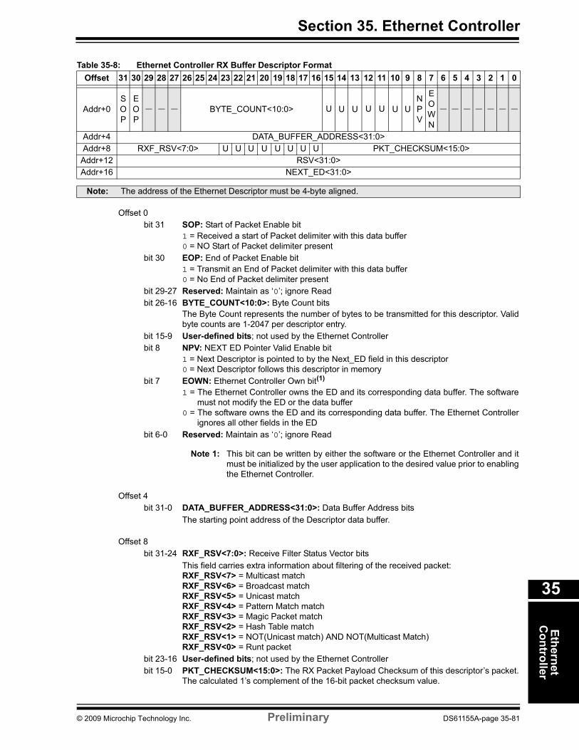
Section 35. Ethernet ControllerEthernet
Controller
35
Table 35-8: Ethernet Controller RX Buffer Descriptor FormatOffset 31 30 29 28 27 26 25 24 23 22 21 20 19 18 17 16 15 14 13 12 11 10 9 8 7 6 5 4 3 2 1 0
Addr+0SOP
EOP
— — — BYTE_COUNT<10:0> U U U U U U UNPV
EOWN
— — — — — — —
Addr+4 DATA_BUFFER_ADDRESS<31:0>Addr+8 RXF_RSV<7:0> U U U U U U U U PKT_CHECKSUM<15:0>Addr+12 RSV<31:0>Addr+16 NEXT_ED<31:0>
Note: The address of the Ethernet Descriptor must be 4-byte aligned.
Offset 0bit 31 SOP: Start of Packet Enable bit
1 = Received a start of Packet delimiter with this data buffer0 = NO Start of Packet delimiter present
bit 30 EOP: End of Packet Enable bit1 = Transmit an End of Packet delimiter with this data buffer0 = No End of Packet delimiter present
bit 29-27 Reserved: Maintain as ‘0’; ignore Readbit 26-16 BYTE_COUNT<10:0>: Byte Count bits
The Byte Count represents the number of bytes to be transmitted for this descriptor. Validbyte counts are 1-2047 per descriptor entry.
bit 15-9 User-defined bits; not used by the Ethernet Controllerbit 8 NPV: NEXT ED Pointer Valid Enable bit
1 = Next Descriptor is pointed to by the Next_ED field in this descriptor0 = Next Descriptor follows this descriptor in memory
bit 7 EOWN: Ethernet Controller Own bit(1)
1 = The Ethernet Controller owns the ED and its corresponding data buffer. The softwaremust not modify the ED or the data buffer
0 = The software owns the ED and its corresponding data buffer. The Ethernet Controllerignores all other fields in the ED
bit 6-0 Reserved: Maintain as ‘0’; ignore Read
Note 1: This bit can be written by either the software or the Ethernet Controller and itmust be initialized by the user application to the desired value prior to enablingthe Ethernet Controller.
Offset 4bit 31-0 DATA_BUFFER_ADDRESS<31:0>: Data Buffer Address bits
The starting point address of the Descriptor data buffer.
Offset 8bit 31-24 RXF_RSV<7:0>: Receive Filter Status Vector bits
This field carries extra information about filtering of the received packet:RXF_RSV<7> = Multicast matchRXF_RSV<6> = Broadcast matchRXF_RSV<5> = Unicast matchRXF_RSV<4> = Pattern Match matchRXF_RSV<3> = Magic Packet matchRXF_RSV<2> = Hash Table matchRXF_RSV<1> = NOT(Unicast match) AND NOT(Multicast Match)RXF_RSV<0> = Runt packet
bit 23-16 User-defined bits; not used by the Ethernet Controllerbit 15-0 PKT_CHECKSUM<15:0>: The RX Packet Payload Checksum of this descriptor’s packet.
The calculated 1’s complement of the 16-bit packet checksum value.
© 2009 Microchip Technology Inc. Preliminary DS61155A-page 35-81

PIC32MX Family Reference Manual
Offset 12bit 31-0 RSV<31:0>: Receive Status Vector bits
Status for the received packet:RSV<31> = ReservedRSV<30> = Receive VLAN Type DetectedCurrent frame was recognized as a VLAN tagged frame.RSV<29> = Receive Unknown Op codeCurrent Frame was recognized as a Control Frame but it contained an Unknown Op-code.Packet does not have a CRC error and has a valid length (64-1518).RSV<28> = Receive Pause Control FrameCurrent Frame was recognized as a Control Frame containing a valid Pause FrameOp-code and a valid address. Packet does not have a CRC error and has a valid length(64-1518).RSV<27> = Receive Control FrameCurrent Frame was recognized as a Control Frame for having a valid Type-Lengthdesignating it as a Control Frame. Packet does not have a CRC error and has a valid length(64-1518).RSV<26> = Dribble NibbleIndicates that after the end of this packet an additional 1 to 7 bits were received. A singlenibble, called the dribble nibble, is formed but not sent out.RSV<25> = Receive Broadcast PacketIndicates packet received had a valid broadcast address.RSV<24> = Receive Multicast PacketIndicates packet received had a valid multicast address.RSV<23> = Received OkIndicates that at the packet had a valid CRC and no symbol errors.RSV<22> = Length Out of RangeIndicates that frame type/length field was larger than 1500 bytes (Type field).RSV<21> = Length Check ErrorIndicates that frame length field value in the packet does not match the actual databyte-length and specifies a valid length.RSV<20> = CRC ErrorIndicates that frame CRC field value does not match the CRC calculated by the receiverMAC.RSV<19> = Receive Code ViolationIndicates that the MII data does not represent a valid receive code when MRXER assertsduring the data phase of a frame.RSV<18> = Carrier Event Previously SeenIndicates that at some time since the last receive statistics, a carrier event was detected,noted and reported with the next receive statistics. The carrier event is not associated withthis packet. A carrier event is activity on the receive channel that does not result in a packetreceive attempt being made. RSV<17> = RXDV Event Previously SeenIndicates that the last receive event seen was not long enough to be a valid packet.RSV<16> = Long Event/Drop EventIndicates a packet over 50,000 bit times occurred, or that a packet since the last RSV wasdropped.RSV<15:0> = Received Byte CountIndicates length of received frame.
Offset 16bit 31-0 NEXT_ED<31:0>: Next Ethernet Descriptor Address bits
When NPV = 1: This field contains the starting point address of the next Ethernet Descriptor.
When NPV = 0: This field is not present in the descriptor.
Table 35-8: Ethernet Controller RX Buffer Descriptor Format (Continued)
DS61155A-page 35-82 Preliminary © 2009 Microchip Technology Inc.

Section 35. Ethernet ControllerEthernet
Controller
35
Figure 35-9: Ethernet Descriptor Table Format (Linked List, NPV = 1)
Packet Buffer
TX/RX Start ADDR (SFR)
Packet Buffer
Packet Buffer
Packet Buffer
STATUS
NEXT_ED
STATUS CHECKSUM/STATUS
DATA_BUFF_ADDR
EOWN BC SOP EOPNPV = 1
STATUS
NEXT_ED
STATUS CHECKSUM/STATUS
DATA_BUFF_ADDR
EOWN BC SOP EOPNPV = 1
STATUS
NEXT_ED
STATUS CHECKSUM/STATUS
DATA_BUFF_ADDR
EOWN BC SOP EOPNPV = 1
STATUS
NEXT_ED
STATUS CHECKSUM/STATUS
DATA_BUFF_ADDR
EOWN BC SOP EOPNPV = 1
© 2009 Microchip Technology Inc. Preliminary DS61155A-page 35-83

PIC32MX Family Reference Manual
Figure 35-10: Ethernet Descriptor Table Format (Linear List, NPV = 0)
35.4.9.1 ETHERNET DESCRIPTOR BUFFER MANAGEMENT
The descriptor tables and packet data buffers used by the receive and transmit paths reside inthe system data memory. The descriptor tables are a linked list of descriptors that referenceblocks of packet data buffers in memory. They are physically and logically partitioned intoseparate Transmit and a Receive Descriptors and Buffers. Note that the start address of both theRX and TX Descriptor tables must be 4-byte-aligned (i.e., bit 1 and bit 0 = 00).
35.4.9.2 ETHERNET DESCRIPTOR OWNERSHIP
Because the descriptors and buffers are shared between the software and the EthernetController, a simple semaphore mechanism is used to distinguish which part is allowed to updatethe descriptor and associated buffers in memory. This semaphore mechanism is implemented bythe EOWN bit in each Buffer Descriptor. When the EOWN bit is clear, the descriptor is owned bythe software. The software may modify the descriptor at its discretion. When the EOWN bit is set,the descriptor (and the buffer memory pointed to by the descriptor) is owned by the EthernetController hardware. The software may not modify the descriptor or its corresponding data buffer.The Ethernet Controller will write the Buffer Descriptor and corresponding data buffer at itsdiscretion.
TX/RX Start ADDR (SFR)
Packet Buffer
STATUS
STATUS CHECKSUM/STATUS
DATA_BUFF_ADDR
STATUS
STATUS CHECKSUM/STATUS
DATA_BUFF_ADDR
STATUS
STATUS CHECKSUM/STATUS
DATA_BUFF_ADDR
EOWN BC SOP EOPNPV = 0
STATUS
STATUS CHECKSUM/STATUS
DATA_BUFF_ADDR
EOWN BC SOP EOPNPV = 1
Packet Buffer
Packet Buffer
NEXT_ED
Packet Buffer
EOWN BC SOP EOPNPV = 0
EOWN BC SOP EOPNPV = 0
DS61155A-page 35-84 Preliminary © 2009 Microchip Technology Inc.

Section 35. Ethernet ControllerEthernet
Controller
35
35.4.9.3 ETHERNET DESCRIPTOR TABLE CONFIGURATION
Before enabling the transfers for the Ethernet Controller, the software must set up both the TXand RX descriptor tables as well as allocate the packet data buffer areas pointed to by thedescriptors. The number of descriptor entries in each table is determined by the software and theamount of memory available in the system.
There are two different types of Ethernet Descriptor Tables (EDTs) that can be set up by software.One configuration is a descriptor ring; the other is a descriptor list. The only difference is whetherthe last descriptor in the list is an “empty” descriptor with the EOWN bit = 0, or the last descriptorhas a reference back to the top of the ring. Either of these can be handled by the Ethernet DMAengines. An example of these two types is shown in Figure 35-11.
35.4.9.4 ETHERNET TRANSMIT BUFFER MANAGEMENT
The Transmit Buffer Management (TXBM) block along with the TX DMA manages the flow oftransmit packets from the system memory to the MAC using the Transmit Buffer Descriptors.
Transmit operation is enabled by setting the TXRTS bit (ETHCON1<9>). In response to theTXRTS bit being set, the TX DMA will fetch an Ethernet Descriptor from the EDT pointed to byETHTXST. After it has read the location of the data buffer and the control word for the data buffer,the DMA will begin reading the data buffer data and writing it to the transmit port of the MAC. Ifmore than one descriptor is needed, the DMA will move to the next descriptor and will continuesending data.
When a packet has to be transmitted from the system memory to the MAC, the packet data isread from the memory pointed by the descriptor DATA_BUFFER_ADDRESS (see Figure 35-9).
The format of the transmitted packets is the same as the one for the received packets. Eachtransmit packet buffer contains the standard Ethernet frame fields to be transmitted (DA, SA,Type/Length and Payload).
An example of a TX packet using 3 descriptors is shown in Figure 35-12.
Once the descriptor table entries and packet data buffers are programmed by the software, thetransmit operation is initiated by setting the TXRTS (ETHCON1<9>) bit.
Once a complete packet has been transmitted, the Ethernet Controller will update the transmitstatus vector (TSV) in the first descriptor entry used for that packet. The EOWN field is updatedfor all descriptors used by the transmitted packet. Also the hardware will update the ETHTXSTregister to reflect the next TX descriptor to be used for the next transmitted packet.
As long as there are valid transmit descriptors for packets (the next descriptor is valid,EOWN = 1), the TX DMA will continue to traverse the descriptor table and send packet data tothe MAC for transmission. When all the transmit operations are complete, the transmit logic willclear the TXRTS bit and set the TXDONE (ETHIRQ<3>) bit. The TXDONE bit will generate aninterrupt if the TXDONEIE (ETHIEN<3>) bit is set. Thus the completion of the transmit operationcan be monitored by either polling the TXRTS bit or by using the TXDONE (ETHIRQ<3>)interrupt.
The transmit operation can be stopped by clearing the TXRTS bit at any time during thetransmission of the packet. When the TXRTS bit is cleared during a packet transmission, thecurrent packet will complete its transmission after which the TXBUSY (ETHSTAT<6>) status bitwill be cleared, indicating the transmit engine has stopped.
Note: It is the responsibility of software to initialize all the fields for each descriptor in theEDT, which includes initializing the status field to 0’s. Refer to Table 35-7 andTable 35-8 for a detailed descriptions of the Ethernet Descriptor format.
Note: Software must insure that the TX descriptor list and ETHTXST register areinitialized prior to setting the TXRTS bit.
Note: The EOWN bits in the transmitted descriptors should be set by software starting withthe last descriptor of the packet to be transmitted and ending with the first. Thisprevents any race condition between software and the Ethernet controllerhardware.
© 2009 Microchip Technology Inc. Preliminary DS61155A-page 35-85

PIC32MX Family Reference Manual
Software should not write any of the TX related SFR registers while the TXRTS bit is set. Tochange these registers, the TXRTS must be cleared, then the software must wait for TXBUSY tode-assert, after which the registers can be written, and the TXRTS bit set again.
35.4.9.5 ETHERNET TRANSMIT OPERATION DETAILS
The packet transmit process is as follows:
1. Software writes the packet data to a packet buffer in data memory and programs adescriptor entry to point to the packet data buffer. It also programs the SOP, EOP,BYTE_COUNT and EOWN bits to show a valid packet is available and also if there areother descriptors needed to send the complete packet. See Figure 35-12 for an exampleof a TX packet using multiple descriptor entries. The descriptor is used to define the Trans-mission Packet data buffer location and length.
2. Software then sets the TXRTS (ETHCON1<9>) bit to start the transmission, which startsthe TX DMA and TXBM logic.
3. The TX DMA engine will read the next available descriptor entry from the descriptor tablewhich is pointed to by the ETHTXST register.
4. After the TX DMA engine reads the DATA_BUFFER_ADDRESS value, the engine willbegin reading the packet data from the location read from the descriptor.
5. The TXBM indicates the start-of-frame to the MAC and transmits the entire frame datafrom the transmit buffer, until the end address is reached. The TXBM simply transmitsfrom the start address until the specified number of bytes has been transmitted to the MACtransmit interface.
6. The MAC can retry a transmission due to an early collision. 7. The MAC can abort a transmission due to a late collision, excessive collisions or exces-
sive defers. This condition is signaled by TXABORT (ETHIRQ<2>).8. Once transmission has completed, the TX DMA engine stores the relevant bits of the TSV
into the first descriptor entry of the packet.9. After the packet has been transmitted, all the descriptors used for the transmission are
released to the software via the EOWN bits being cleared.10. If more valid TX descriptors are available (EOWN = 1), the DMA engine will go back to
step 3 to begin the next packet’s transmission. Otherwise, if the next descriptor is stillowned by hardware (EOWN = 0), transmission will halt and wait for the software to set theTXRTS bit again.
Note that any collision that occurs within the CWINDOW (EMACxCLRT<8:14>) boundary is anearly collision and results in a Retry operation. A collision that happens beyond the CWINDOWboundary will be treated as a late collision and will cause an abort. The CWINDOW bit in theEMACxCLRT register is typically set to 64 bytes. An abort condition can also result from reachingthe maximum collision count RETX (EMACxCLRT<0:3>) for a packet trying to be sent.
Note: The ETHTXST transmit configuration register (starting address of TX DescriptorTable) is used by the TX DMA, and should only be changed when the TX DMA isnot operating (i.e., TXRTS (ETHCON1<9>) = 0 and TXBUSY (ETHSTAT<6>) = 0 ),since continual synchronization to the DMA clock domain is not provided.Ensuring the ETHTXST configuration register does not change when the TX DMAis active is the responsibility of software.
DS61155A-page 35-86 Preliminary © 2009 Microchip Technology Inc.

Section 35. Ethernet ControllerEthernet
Controller
35
The TXBM engine has little information about the content of data it sends to the MAC. However,it should be noted that two kinds of transmit packets can be sent:
1. A complete packet, which includes the following:• Addresses (DA, SA), Type/Length and Payload• Pad (if required)• Frame Check Sequence
In this case, PADENABLE (EMACxCFG2<5>) bit is 0. The MAC will not pad the frame,but will perform a CRC check on the frame, and set TSV<20> in the TX status vector ifthe CRC check match fails.
2. An incomplete packet that includes:• Addresses (DA, SA), Type/Length and Payload
In this case, PADENABLE = 1. The MAC will pad the frame (in accordance with the set-tings of AUTOPAD, VLANPAD (EMACxCFG2<7:6>)), and will insert the calculatedCRC (FCS) for the frame.
See Table 35-2 for a description of the pad and CRC options based on the settings of theEMACxCFG2 register.
© 2009 Microchip Technology Inc. Preliminary DS61155A-page 35-87

PIC32MX Family Reference Manual
Example 35-4: Ethernet Transmit Packet Code/*The following assumptions were made for this example:- the packet that has to be sent consists of multiple buffers in memory.- the number of available TX descriptors greater than the number of buffers composing the packet (there's at least an extra descriptor ending the chain of descriptors)- this is the first transmission of a packet, the example enables the transmission process.*//*Input parameters:- sEthTxDcpt* pArrDcpt: pointer to an array that holds free descriptors that we can use for the TX operation (see below the definition for sEthTxDcpt).- char* pArrBuff: pointer to an array that holds buffers to be transmitted- int* pArrSize: pointer to an array that holds the sizes of buffers to be transmitted- int nArrayItems: how many buffers to be transmitted are stored in the array.*/
#include <p32xxxx.h>// definition used for this example (see Table 35-7: Ethernet Controller TX Buffer Descriptor Format)
typedef struct {
volatile union{
struct{
unsigned: 7;unsigned EOWN: 1;unsigned NPV: 1;unsigned: 7;unsigned bCount: 11;unsigned: 3;unsigned EOP: 1;unsigned SOP: 1;
};unsigned intw;
}hdr; // descriptor headerunsigned char*pEDBuff; // data buffer addressvolatile unsigned long longstat; // tx packet statusunsigned intnext_ed; // next descriptor (hdr.NPV==1);
}__attribute__ ((__packed__)) sEthTxDcpt; // hardware Tx descriptor (linked).
extern void* VA_TO_PA(char* pBuff); // extern function that returns the physical// address of the virtual address input parameter
int ix; // loop indexsEthTxDcpt* pEDcpt; // current Ethernet descriptorsEthTxDcpt* tailDcpt; // last Ethernet descriptorchar* pBuff; // current data buffer to be transmittedint* pSize; // current data buffer size
pEDcpt=pArrDcpt;pBuff=pArrBuff;pSize=pArrSize;tailDcpt=0;
for(ix=0; ix< nArrayItems; ix++, pEDcpt++, pBuff++, pSize++) {
// pass the descriptor to hw, use linked descriptors, set proper sizepEDcpt->pEDBuff=(unsigned char*)VA_TO_PA(pBuff); // set bufferpEDcpt->hdr.w=0; // clear all the fieldspEDcpt-> hdr.NPV= 1; // set next pointer validpEDcpt-> hdr.EOWN= 1; // set hw ownershippEDcpt->hdr.bCount=*pSize; // set proper size
if(tailDcpt){tailDcpt->next_ed=VA_TO_PA(&pEDcpt);}tailDcpt=pEDcpt;
}
DS61155A-page 35-88 Preliminary © 2009 Microchip Technology Inc.
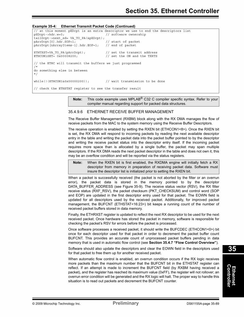
Section 35. Ethernet ControllerEthernet
Controller
35
Example 35-4: Ethernet Transmit Packet Code (Continued)
35.4.9.6 ETHERNET RECEIVE BUFFER MANAGEMENT
The Receive Buffer Management (RXBM) block along with the RX DMA manages the flow ofreceive packets from the MAC to the system memory using the Receive Buffer Descriptors.
The receive operation is enabled by setting the RXEN bit (ETHCON1<8>). Once the RXEN bitis set, the RX DMA will respond to incoming packets by reading the next available descriptorentry in the table and writing the packet data into the packet buffer pointed to by the descriptorand writing the receive packet status into the descriptor entry itself. If the incoming packetrequires more space than is allocated by a single buffer, the packet may span multipledescriptors. If the RX DMA reads the next packet descriptor in the table and does not own it, thismay be an overflow condition and will be reported via the status registers.
When a packet is successfully received (the packet is not aborted by the filter or an overrunerror), the packet data is stored in the memory pointed to by the descriptorDATA_BUFFER_ADDRESS (see Figure 35-9). The receive status vector (RSV), the RX filterreceive status (RXF_RSV), the packet checksum (PKT_CHECKSUM) and control word (SOPand EOP) are updated in the first descriptor entry used for that packet. The EOWN field isupdated for all descriptors used by the received packet. Additionally, for improved packetmanagement, the BUFCNT (ETHSTAT<16:23>) bit keeps a running count of the number ofreceived packet buffers stored in data memory.
Finally, the ETHRXST register is updated to reflect the next RX descriptor to be used for the nextreceived packet. Once hardware has stored the packet in memory, software is responsible forchecking the packet’s RSV for errors before the packet is processed.
Once software processes a received packet, it should write the BUFCDEC (ETHCON1<0>) bitonce for each descriptor used for that packet in order to decrement the packet buffer countBUFCNT. This provides an accurate count of unprocessed packet buffers pending in datamemory that is used in automatic flow control (see Section 35.4.7 “Flow Control Overview”).
Software should also update the descriptors and clear the EOWN field in the descriptors usedfor that packet to free them up for another received packet.
When automatic flow control is enabled, an overrun condition occurs if the RX logic receivesmore packets than the maximum number that the BUFCNT bit in the ETHSTAT register canreflect. If an attempt is made to increment the BUFCNT field (by RXBM having received apacket), and the register has reached its maximum value (0xFF), the register will not rollover; anoverrun error condition will be generated and the RX logic will halt. The proper way to handle thissituation is to read out packets and decrement the BUFCNT counter.
// at this moment pEDcpt is an extra descriptor we use to end the descriptors listpEDcpt->hdr.w=0; // software ownershiptailDcpt->next_ed= VA_TO_PA(&pEDcpt);pArrDcpt[0].hdr.SOP=1; // start of packetpArrDcpt[nArrayItems-1].hdr.EOP=1; // end of packet
ETHTXST=VA_TO_PA(pArrDcpt); // set the transmit addressETHCON1SET= 0x00008200; // set the ON and the TXRTS
// the ETHC will transmit the buffers we just programmed/*do something else in between*/
while(!(ETHCON1&0x00000200)); // wait transmission to be done
// check the ETHSTAT register to see the transfer result
Note: This code example uses MPLAB® C32 C compiler specific syntax. Refer to yourcompiler manual regarding support for packed data structures.
Note: When the RXEN bit is first enabled, the RXDMA engine will initially fetch a RXdescriptor from memory in preparation of receiving packet data. Software mustinsure the descriptor list is initialized prior to setting the RXEN bit.
© 2009 Microchip Technology Inc. Preliminary DS61155A-page 35-89

PIC32MX Family Reference Manual
If automatic flow control is disabled, the RXDMA will continue processing and BUFCNT willsaturate at a value of 0xFF.
If the RX engine stops due to a lack of available descriptors, it will not start again until it detectsa write to the BUFCDEC (ETHCON1<0>) bit. This signals that the software has freed upadditional RX descriptor buffers.
35.4.9.7 ETHERNET RECEIVE OPERATION DETAILS
A received packet is stored in the packet buffer along with a status vector, which is stored in thedescriptor. The status vector has two components:
• The Receive Status Vector (RSV), which is driven by the MAC at the end of a received packet, and contains information about the packet received.
• The Receive Filter Status vector (RXF_RSV) driven out by the RX Filter block.
This combined status is stored in the first descriptor used to store the packet data buffer.
The sequence of steps involved in the receiving process is as follows:
1. Software sets up the RX descriptor table with RX descriptor entries and the associatedpacket data buffers pointed to by each descriptor entry.
2. Software writes to the ETHRXST register (pointing to the start of the RX descriptor table)and enables the RX port by setting the RXEN (ETHCON1<8>) bit.
3. The RX DMA engine reads a valid descriptor from the table and determines the start ofthe packet data buffer.
4. When a packet is received, the MAC indicates the start of a new frame and presents thedata.
5. The RXBM receives the data and stores it in an RX FIFO. Writes to the system memoryare postponed until 32 bits of data have been received. The RX DMA takes the data fromthe RX FIFO and stores it in the Packet data buffer pointed to by the descriptor it just read.Once all the bytes are written that have been allocated by the descriptor, the RX DMAreads another descriptor in order to write more packet data.
6. If the RX DMA fetches a descriptor with EOWN = 0 when needed to store more packetdata, a RXBUFNA (ETHIRQ<1>) interrupt occurs.
7. If any of the following events occur during a packet reception, the packet is aborted andthe descriptor is not updated with the packet status, which leaves it available for the nextpacket:• The RX Filter aborts the packet • RXFIFO overrun, which can be caused by:
- excessive system level latency- BUFCNT (ETHSTAT<16:23>) reaching maximal value- No descriptors are available for hardware processing
8. Once the frame completes, the MAC presents the Receive Status Vector (RSV) and theRX Filter presents the Receive Filter Status Vector (RXF_RSV).
9. The RX DMA will traverse the descriptors a second time:a) The first descriptor used for the current packet will be updated with the RSV,
RXF_RSV, PKT_CHECKSUM and BYTE_COUNT values. b) All the descriptors belonging to the current packet get their SOP and EOP updated.
Also the EOWN bit is changed to signal to software that it can read the packet data.10. Once the RSV is passed to the RX DMA, the RXBM is ready to receive another packet.
Note 1: The ETHRXST receive configuration register (starting address of RX DescriptorTable) is used by the RX DMA, and should only be changed when the RX DMA isnot operating (i.e., RXEN (ETHCON1<8>) = 0 and RXBUSY (ETHSTAT<5>) = 0),since continual synchronization to the DMA clock domain is not provided.Ensuring the ETHRXST configuration register does not change when the RX DMAis active is the responsibility of software.
2: When using an RX EDT ring, the software must make sure that the RX EDT con-tains (at a minimum) enough entries that are required to buffer the largest Ethernetframe. This is needed because the RX DMA engine does not detect thewrap-around condition.
DS61155A-page 35-90 Preliminary © 2009 Microchip Technology Inc.
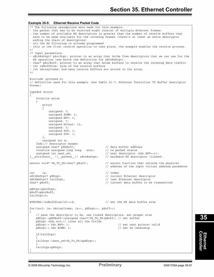
Section 35. Ethernet ControllerEthernet
Controller
35
Example 35-5: Ethernet Receive Packet Code/* The following assumptions were made for this example:- the packet that has to be received might consist of multiple Ethernet frames.- the number of available RX descriptors is greater than the number of receive buffers that
have to be made available for the incoming frames (there’s at least an extra descriptorending the chain of descriptors)
- all the RX filtering is already programmed- this is the first receive operation to take place, the example enables the receive process.*//* Input parameters:- sEthRxDcpt* pArrDcpt: pointer to an array that holds free descriptors that we can use for the
RX operation (see below the definition for sEthRxDcpt).- char* pArrBuff: pointer to an array that holds buffers to receive the incoming data traffic- int rxBuffSize: size of the receive buffers- int nArrayItems: how many receive buffers are stored in the array.*/
#include <p32xxxx.h>// definition used for this example (see Table 35-7: Ethernet Controller TX Buffer Descriptor Format)
typedef struct {
volatile union{
struct{
unsigned: 7;unsigned EOWN: 1;unsigned NPV: 1;unsigned: 7;unsigned bCount: 11;unsigned: 3;unsigned EOP: 1;unsigned SOP: 1;
};unsigned int w;
}hdr;// descriptor headerunsigned char* pEDBuff; // data buffer addressvolatile unsigned long long stat; // tx packet statusunsigned int next_ed; // next descriptor (hdr.NPV==1);
}__attribute__ ((__packed__)) sEthRxDcpt; // hardware RX descriptor (linked).
extern void* VA_TO_PA(char* pBuff); // extern function that returns the physical// address of the input virtual address parameter
int ix; // indexsEthRxDcpt* pEDcpt; // current Ethernet descriptorsEthRxDcpt* tailDcpt; // last Ethernet descriptorchar* pBuff; // current data buffer to be transmitted
pEDcpt=pArrDcpt;pBuff=pArrBuff;tailDcpt=0;
ETHCON2=(rxBuffSize/16)<<4; // set the RX data buffer size
for(ix=0; ix< nArrayItems; ix++, pEDcpt++, pBuff++) {
// pass the descriptor to hw, use linked descriptors, set proper sizepEDcpt->pEDBuff=(unsigned char*)VA_TO_PA(pBuff); // set bufferpEDcpt->hdr.w=0;// clear all the fieldspEDcpt-> hdr.NPV= 1; // set next pointer validpEDcpt-> hdr.EOWN= 1; // set hw ownership
if(tailDcpt){tailDcpt->next_ed=VA_TO_PA(&pEDcpt);}tailDcpt=pEDcpt;
}
© 2009 Microchip Technology Inc. Preliminary DS61155A-page 35-91
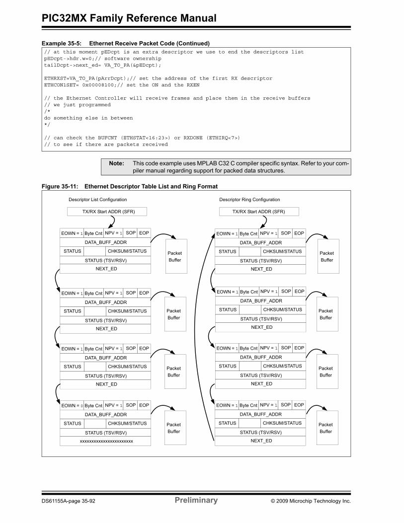
PIC32MX Family Reference Manual
Example 35-5: Ethernet Receive Packet Code (Continued)
Figure 35-11: Ethernet Descriptor Table List and Ring Format
// at this moment pEDcpt is an extra descriptor we use to end the descriptors listpEDcpt->hdr.w=0;// software ownershiptailDcpt->next_ed= VA_TO_PA(&pEDcpt);
ETHRXST=VA_TO_PA(pArrDcpt);// set the address of the first RX descriptorETHCON1SET= 0x00008100;// set the ON and the RXEN
// the Ethernet Controller will receive frames and place them in the receive buffers// we just programmed/*do something else in between*/
// can check the BUFCNT (ETHSTAT<16:23>) or RXDONE (ETHIRQ<7>) // to see if there are packets received
Note: This code example uses MPLAB C32 C compiler specific syntax. Refer to your com-piler manual regarding support for packed data structures.
Packet Buffer
TX/RX Start ADDR (SFR)
STATUS (TSV/RSV)
NEXT_ED
DATA_BUFF_ADDR
NPV = 1EOWN = 1 Byte Cnt EOPSOP
CHKSUM/STATUSSTATUS
Descriptor List Configuration Descriptor Ring Configuration
Packet Buffer
Packet Buffer
Packet Buffer
Packet Buffer
TX/RX Start ADDR (SFR)
Packet Buffer
Packet Buffer
Packet Buffer
STATUS (TSV/RSV)
NEXT_ED
DATA_BUFF_ADDR
NPV = 1EOWN = 1 Byte Cnt EOPSOP
CHKSUM/STATUSSTATUS
STATUS (TSV/RSV)
NEXT_ED
DATA_BUFF_ADDR
NPV = 1EOWN = 1 Byte Cnt EOPSOP
CHKSUM/STATUSSTATUS
STATUS (TSV/RSV)
xxxxxxxxxxxxxxxxxxxxxxx
DATA_BUFF_ADDR
NPV = 1EOWN = 0 Byte Cnt EOPSOP
CHKSUM/STATUSSTATUS
STATUS (TSV/RSV)
NEXT_ED
DATA_BUFF_ADDR
NPV = 1EOWN = 1 Byte Cnt EOPSOP
CHKSUM/STATUSSTATUS
STATUS (TSV/RSV)
NEXT_ED
DATA_BUFF_ADDR
NPV = 1EOWN = 1 Byte Cnt EOPSOP
CHKSUM/STATUSSTATUS
STATUS (TSV/RSV)
NEXT_ED
DATA_BUFF_ADDR
NPV = 1EOWN = 1 Byte Cnt EOPSOP
CHKSUM/STATUSSTATUS
STATUS (TSV/RSV)
NEXT_ED
DATA_BUFF_ADDR
NPV = 1EOWN = 1 Byte Cnt EOPSOP
CHKSUM/STATUSSTATUS
DS61155A-page 35-92 Preliminary © 2009 Microchip Technology Inc.
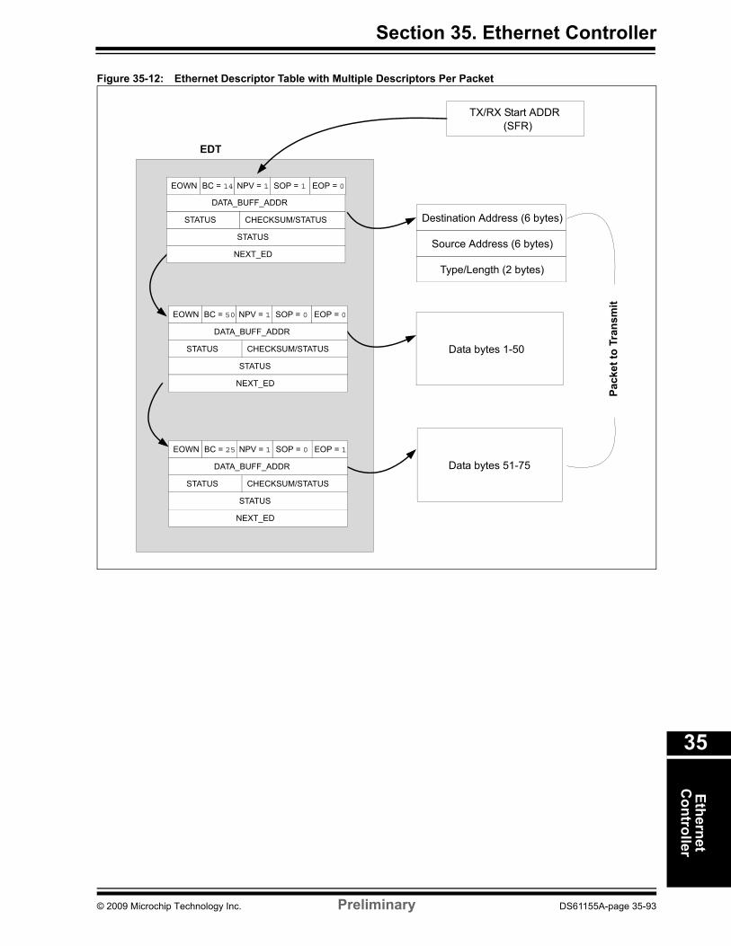
Section 35. Ethernet ControllerEthernet
Controller
35
Figure 35-12: Ethernet Descriptor Table with Multiple Descriptors Per Packet
TX/RX Start ADDR (SFR)
Data bytes 1-50
Data bytes 51-75
Type/Length (2 bytes)
Source Address (6 bytes)
Destination Address (6 bytes)
STATUS
NEXT_ED
STATUS CHECKSUM/STATUS
DATA_BUFF_ADDR
EOWN BC = 25 SOP = 0 EOP = 1NPV = 1
STATUS
NEXT_ED
STATUS CHECKSUM/STATUS
DATA_BUFF_ADDR
STATUS
NEXT_ED
STATUS CHECKSUM/STATUS
DATA_BUFF_ADDR
EDT
Pack
et to
Tra
nsm
it
EOWN BC = 50 SOP = 0 EOP = 0NPV = 1
EOWN BC = 14 SOP = 1 EOP = 0NPV = 1
© 2009 Microchip Technology Inc. Preliminary DS61155A-page 35-93

PIC32MX Family Reference Manual
35.4.10 Ethernet Initialization SequenceIn order to initialize the Ethernet Controller to receive and transmit Ethernet messages, Microchiprecommends that this sequence of steps be followed:1. Ethernet Controller Initialization:
a) Disable Ethernet interrupts in the EVIC by clearing bit ETHIE (IEC1<28>).b) Turn the Ethernet Controller off, and then clear the ON, RXEN and TXEN bits
(ETHCON1<15>, ETHCON1<8> and ETHCON1<9>).c) Wait activity abort by polling the ETHBUSY bit (ETHSTAT<7>).d) Clear the Ethernet Interrupt Flag (ETHIF) bit in the Interrupts module (IFS1<28>).e) Disable any Ethernet Controller interrupt generation by clearing the ETHIRQIE
register.f) Clear the TX and RX start addresses by using ETHTXSTCLR and ETHRXSTCLR.
2. MAC Init:a) Reset the MAC using SOFTRESET (EMACxCFG1<15>) or individually reset the
modules setting the RESETRMCS, RESETRFUN, RESETTMCS, RESETTFUN bits(EMACxCFG1<11:8>).
b) Use the configuration fuse setting FETHIO (DEVCFG3<25>) to detect thealternate/default I/O configuration (Refer to Section 32. “Configuration” for details).
c) Use the configuration fuse setting FMIIEN (DEVCFG3<24>) to detect the MII/RMIIoperation mode.
d) Properly initialize as digital, all the pins used by the MAC - PHY interface (normallyonly those pins that have shared analog functionality need to be configured).
e) Initialize the MIIM interface:i. If the RMII operation is selected, reset the RMII module by using the RESETRMII
(EMACxSUPP<11>) bit and set the proper speed in the SPEEDRMII(EMACxSUPP<8>) bit.
ii. Issue an MIIM block reset, by setting the RESETMGMT (EMACxMCFG<15>) bit,and then clear the reset bit.
iii. Select a proper divider in the CLKSEL (EMACxCFG<5:2>) bit for the MIIM PHYcommunication based on the system running clock frequency and the externalPHY supported clock.
3. PHY Init:This depends on the actual external PHY used. All PHYs should implement the basic reg-ister set as stated in Clause 22, Table 22-6-MII Management Register Set of the IEEE802.3 Standard.In addition to the basic register set, PHYs may provide an extended set of nine registersand capabilities that may be accessed and controlled via the MIIM interface. They providea PHY-specific identifier, control and monitoring for the Auto-Negotiation process, etc.The IEEE 802.3 Standard provides room for 16 extended registers, which implementvendor-specific capabilities.Following is a list of common initialization steps that should be taken. Adjust accordinglyby refering the vendor-specific PHY data sheet.a) Reset the PHY (use Control Register 0).b) Set the MII/RMII operation mode. This usually requires access to a vendor-specific
control register.c) Set the normal, swapped or auto (preferred) MDIX. This usually requires access to a
vendor-specific control register.d) Check the PHY capabilities by investigating the Status Register 1.e) Preferably the auto-negotiation should be selected if the PHY supports it. Expose the
supported capabilities: Half/Full Duplex, 10BaseT/100Base TX, etc. (ExtendedRegister 4). Start the negotiation (Control Register 0) and wait for the negotiationcomplete and get the link partner capabilities (Extended Register 5) and negotiationresult (vendor-specific register).
f) If auto-negotiation is not supported/selected, update the PHY Duplex and Speedsettings directly (use Control Register 0 and possibly some vendor-specific registers).
DS61155A-page 35-94 Preliminary © 2009 Microchip Technology Inc.
Section 35. Ethernet ControllerEthernet
Controller
35
4. MAC Configuration:
Having available the Duplex and Speed settings, configure the MAC accordingly, usingthe following steps:
a) Enable the RXENABLE (EMACxCFG1<0>) bit, selecting both the TXPAUSE andRXPAUSE (EMACxCFG1<3,2>) (the PIC32MX MAC supports both).
b) Select the desired auto-padding and CRC capabilities, and the enabling of the hugeframes and the Duplex type in the EMACxCFG2 register.
c) Program EMACxIPGT with the back-to-back inter-packet gap.d) Use EMACxIPGR for setting the non back-to-back inter-packet gap.e) Set the collision window and the maximum number of retransmissions in
EMACxCLRT.f) Set the maximum frame length in EMACxMAXF.g) Optionally set the station MAC address in the EMACxSA0, EMACxSA1 and
EMACxSA2 registers (these registers are loaded at reset from the factorypreprogrammed station address).
5. Continue the Ethernet Controller Initialization:a) If planning to turn on the flow control, update the PTV value (ETHCON1<31:16>).b) If using the auto-flow control, set the full and empty watermarks: RXFWM and
RXEWM (ETHRXWM<23:16> and ETHRXWM<7:0>).c) If needed, enable the auto-flow control by setting AUTOFC (ETHCON1<7>).d) Set the RX filters by updating the ETHHT0, ETHHT1, ETHPMM0, ETHPMM1,
ETHPMCS and ETHRXFC registers.e) Set the size of the RX buffers in the RXBUFSZ (ETHCON2<10:4>) bits (all receive
descriptors use the same buffer size). Keep in mind that using packets that are toosmall leads to packet fragmentation and has a noticeable impact on the performance.
f) Prepare a list/ring of TX descriptors for messages to be transmitted. Properly updateall the fields in the TX descriptor (NPV, EOWN = 1, NEXT_ED) (see Table 35-7,“Ethernet Controller TX Buffer Descriptor Format”). If using a list, end it properly witha software own descriptor (EOWN = 0).
The SOP, EOP, DATA_BUFFER_ADDRESS and BYTE_COUNT will be updatedwhen a particular message has to be transmitted. The DATA_BUFFER_ADDRESSwill contain the physical address of the message, the BYTE_COUNT message size.SOP and EOP are set depending on how many packets are needed to transmit themessage.
g) Prepare a list of RX descriptors populated with valid buffers for messages to bereceived. Properly update the NPV, EOWN = 1 and DATA_BUFFER_ADDRESSfields in the RX descriptors (see Table 35-8, “Ethernet Controller RX Buffer DescriptorFormat”). The DATA_BUFFER_ADDRESS should contain the physical address ofthe corresponding RX buffer.
h) The actual number of RX/TX descriptors and RX previously allocated buffersdepends on your actual system memory availability and on the intended Ethernettraffic you anticipate and want to handle.
i) Update the ETHTXST register with the physical address of the head of the TXdescriptors list.
j) Update the ETHRXST register with the physical address of the head of the RXdescriptors list.
k) Enable the Ethernet Controller by setting the ON bit (ETHCON1<15).l) Enable the receiving of messages by setting the RXEN bit (ETHCON1<8>).m) Inspect the list of RX descriptors to see if the EOWN bit is cleared. If it is, this descrip-
tor is now under software control and a message was received. Use SOP and EOPto extract the message, use BYTE_COUNT, RXF_RSV, RSV and PKT_CHECKSUMto get the message characteristics.
© 2009 Microchip Technology Inc. Preliminary DS61155A-page 35-95

PIC32MX Family Reference Manual
n) In order to transmit a message:i. First make sure that the message has the proper format according the Ethernet
Frame specifications.ii. Update the necessary number of TX descriptors, starting with the head of the list,
by setting the DATA_BUFFER_ADDRESS to be the physical address of thecorresponding buffer in the message to be transmitted.
iii. Keep in mind that large packet fragmentation has an impact on the performance.iv. Update BYTE_COUNT for each descriptor with the number of bytes contained
in each buffer.v. Set EOWN = 1 for each descriptor that belongs to the packet.vi. Use SOP and EOP to specify that the message uses one or more TX descriptors.
o) Enable the transmission of the message, set the TXRTS (ETHCON1<9>) bit.p) Inspect the list of TX descriptors to see if the EOWN bit is cleared. If it is, this descrip-
tor is now under software control and the message was transmitted. Use TSV tocheck for the transmission result.
35.4.11 Ethernet Statistics RegistersTo comply with the 802.3 Layer Management specification, the Ethernet Controller implementsvarious statistics registers in hardware. These registers are incremented by hardware whenvarious conditions are detected in a transmitted/received packet. Once a register reached itsmaximum value, it will roll over to all zeros the next time it is incremented. Therefore, it is theresponsibility of software to read these in a timely manner to avoid losing any data.
A read by software will automatically cause the corresponding register to be cleared.
Statistics counters can be written by software using the SET, CLR and INV registers. Writes tothe normal registers are also supported. In normal operation, the statistics registers should justbe read on a periodic basis to collect data on the Ethernet link traffic.
35.4.11.1 PAYLOAD CHECKSUM CALCULATION
The Ethernet Controller automatically calculates a 16-bit packet checksum for all receivedpackets and stores the 16-bit value along with the received packets status vector in the packetdescriptor PKT_CHECKSUM field (RX_DCPT<96:111>). This checksum can be useful forTCP/IP software implementations.
The payload checksum is calculated over the complete received packet except for the first 14bytes (destination address, source address and length/type fields). If software needs to excludemore bytes from the checksum, it must subtract the values out.
A payload checksum is a simple checksum used to provide basic protection against bit corruptionduring transmission. It is typically used in TCP and UDP packets of the TCP/IP protocols. Thechecksum is calculated by dividing the byte stream into 16-bit words and adding them together.Any overflow is also added back into the sum. The checksum calculation begins after the first 14bytes of the frame are received and includes the FCS bytes. The result is the 1’s complement ofthe calculated sum.
Refer to Figure 35-7 for an example of payload checksum calculation.
Note 1: The SET, CLR and INV Statistics registers are meant only for supporting softwaredebugging and testing.
2: When the device is put in Sleep mode, updates to the statistics registers aresuspended as the system clock is not running. The only exception to this is anoverflow case, which will increment the overflow counter and set the overflow flagRXOVFLW (ETHIRQ<0>) bit. This is done to signal to software upon a wake-upthat some packets have been lost.
3: Some statistical counters may immediately increment when exiting Sleep due topending events.
DS61155A-page 35-96 Preliminary © 2009 Microchip Technology Inc.

Section 35. Ethernet ControllerEthernet
Controller
35
35.5 ETHERNET INTERRUPTSThe PIC32MX device has the ability to generate interrupts reflecting the events that occur duringthe Ethernet Controller’s transfer of frames. Each of the Ethernet Controller interrupt events hasa corresponding interrupt enable bit in the ETHIEN register, which must be set for an interrupt tobe generated. However, regardless of the value of the ETHIEN register, the status of all interruptevents is directly readable via the ETHIRQ register. Therefore, the software has visibility of anevent generating a potential interrupt by polling the register and not having an interrupt propagateout of the module.Ethernet interrupts are persistent. This means that as long as the event that generated theinterrupt is pending, the interrupt signal from the Ethernet Controller module will remain asserted.Following is a description of the interrupt events generated by the transmission and receive ofEthernet frames.Transmit path related interrupt events:
• TX DMA engine transfer error interrupt, signaled by the TXBUSE (ETHIRQ<14>) bit and enabled using the TXBUSEIE (ETHIEN<14>) bit. This event occurs when the TX DMA encounters a bus error during a memory access and is caused by an addressing error (usually because of a bad pointer).
• Transmission done interrupt, signaled by the TXDONE (ETHIRQ<3>) bit and enabled using the TXDONEIE (ETHIEN<3>) bit. This event occurs when the currently transmitted TX packet completes transmission and the Transmit Status Vector is loaded into the first descriptor of the packet.
• Transmission aborted interrupt, signaled by the TXABORT (ETHIRQ<2>) bit and enabled using the TXABORTIE (ETHIEN<2>) bit. This event occurs when the MAC aborts the transmission because of one of the following reasons:- Jumbo TX packet abort (The size of the packet is greater than the maximum size
MACMAXF (EMACxMAXF<15:0>))- Underrun abort (The transmit engine cannot keep up with the requested data flow. This
usually happens when the system bus is overloaded.)- Excessive defer abort (Packet was deferred in excess of 6071 nibble times in 100
Mbps mode or 24,287 bit times in 10 Mbps mode)- Late collision abort (Collision occurred beyond the collision window)- Excessive collisions abort (Packet was aborted because the number of collisions
exceeded RETX (EMACxCLRT<3:0>))
Receive path related interrupt events:
• RX DMA engine transfer error interrupt, signaled by the RXBUSE (ETHIRQ<13>) bit and enabled using the RXBUSEIE (ETHIEN<13>) bit. This event occurs when the RX DMA encounters a bus error during a memory access and is caused by an addressing error (usually because of a bad pointer).
• Receive done interrupt, signaled by the RXDONE (ETHIRQ<7>) bit and enabled using the RXDONEIE (ETHIEN<7>) bit. This event occurs whenever a packet is successfully received.
• Packet pending interrupt, signaled by the PKTPEND (ETHIRQ<6>) bit and enabled using the PKTPENDIE (ETHIEN<6>) bit. This event occurs whenever the buffer counter BUFCNT (ETHSTAT<16:23>) has a value greater than 0.
• Receive Activity interrupt, signaled by the RXACT (ETHIRQ<5>) bit and enabled using the RXACTIE (ETHIEN<5>) bit. This event occurs whenever there is data stored in the RXBM FIFO.
• Receive buffer not available interrupt, signaled by the RXBUFNA (ETHIRQ<1>) bit and enabled using the RXBUFNAIE (ETHIEN<1>) bit. This event occurs whenever the RX DMA runs out of descriptors by fetching a descriptor not owned by hardware (EOWN = 0).
Note: An early collision will cause the MAC to assert the Retry, but not the Abort. Thiscondition will therefore not cause an interrupt.
© 2009 Microchip Technology Inc. Preliminary DS61155A-page 35-97

PIC32MX Family Reference Manual
• Receive FIFO overflow error interrupt, signaled by the RXOVFLW (ETHIRQ<0>) bit and enabled using the RXOVFLIE (ETHIEN<0>) bit. This event occurs whenever the RXBM is unable to transfer data out of the receive FIFO to the system memory and the internal FIFO overflows because of one of the following reasons:- Excessive system level latency- BUFCNT (ETHSTAT<16:23>) reaching maximal value- No descriptors are available for hardware processing
• Empty Watermark interrupt, signaled by the EWMARK (ETHIRQ<9>) bit and enabled using the EWMARKIE (ETHIEN<9>) bit. This event occurs whenever the RX descriptor buffer count BUFCNT (ETHSTAT<16:23>) is less than or equal to the RXEWM ETHRXWM<0:7>) value.
• Full Watermark interrupt, signaled by the FWMARK (ETHIRQ<8>) bit and enabled using the FWMARKIE (ETHIEN<8>) bit. This event occurs whenever the RX descriptor buffer count BUFCNT (ETHSTAT<16:23>) is greater than or equal to the RXFWM (ETHRXWM<16:23>) value.
Also, interrupts in the Ethernet peripheral could be divided into two types, depending on how andwhere the interrupt is cleared. They are software cleared interrupt events and hardware clearedinterrupt events. Note that all the interrupt events are cleared by a device Reset.
Software cleared interrupt events are cleared by writing the corresponding bit in the ETHIRQCLRregister or the ETHIRQ register directly, and include the following:
• TXBUSE• RXBUSE• RXDONE• RXACT• TXDONE• TXABORT• RXBUFNA• RXOVFLW
Hardware cleared interrupt events are cleared by removing the condition that caused theinterrupt, and include the following:
• EWMARK – This interrupt can be cleared when an RX packet is successfully received and the BUFCNT value is greater than the RXEWM (ETHRXWM<0:7>) value.
• FWMARK – This interrupt can be cleared by writing to the BUFCDEC (ETHCON1<0>) bit, thereby decrementing the buffer descriptor count (BUFCNT) below the RXFWM (ETHRXWM<16:23>) value.
• PKTPEND – This interrupt can be cleared by writing the BUFCDEC bit until BUFCNT (ETHSTAT<16:23>) reaches ‘0’.
All the interrupts belonging to the Ethernet controller map to the Ethernet interrupt vector.
The corresponding Ethernet Controller interrupt flag is ETHIF (IFS1<28>). This interrupt flagmust be cleared in software once the cause generating the interrupt is processed.
The Ethernet controller is enabled as a source of interrupts via the respective Ethernet Controllerinterrupt enable bit ETHIE (IEC1<28>).
The interrupt priority-level bits and interrupt subpriority-level bits must also be configured:
• ETHIP<2:0> (IPC12<4:2>)• ETHIS<1:0> (IPC12<1:0>)
Note: Refer to Section 8. “Interrupts” (DS61108) for detailed descriptions of the IFSx,IECx and IPCx interrupt bits.
DS61155A-page 35-98 Preliminary © 2009 Microchip Technology Inc.

Section 35. Ethernet ControllerEthernet
Controller
35
35.5.1 Interrupt ConfigurationThe Ethernet controller internally has multiple interrupt flags (TXBUSE, RXBUSE, EWMARK,FWMARK, RXDONE, PKTPEND, RXACT, TXDONE, TXABORT, RXBUFNA, RXOVFLW) andcorresponding enable interrupt control bits (TXBUSEIE, RXBUSEIE, EWMARKIE, FWMARKIE,RXDONEIE, PKTPENDIE, RXACTIE, TXDONEIE, TXABORTIE, RXBUFNAIE, RXOVFLIE).However, for the interrupt controller, there is just one dedicated interrupt flag bit for the EthernetController: ETHIF (IFS1<28>) and the corresponding interrupt enable/mask bit: ETHIE(IEC1<28>).
The Ethernet Controller has its own priority and sub-priority levels independent of otherperipherals. Note that the ETHIF bit will be set without regard to the state of the correspondingenable bit ETHIE. The ETHIF bit can be polled by software if desired.
The ETHIE bit is used to define the behavior of the Vector Interrupt Controller (INT) module whena corresponding ETHIF bit is set. When the corresponding ETHIE bit is clear, the Interruptsmodule does not generate a CPU interrupt for the event. If the ETHIE bit is set, the Interruptsmodule will generate an interrupt to the CPU when the ETHIF bit is set (subject to the priority andsub-priority as follows).
It is the responsibility of the user’s software routine that services a particular interrupt to clear theinterrupt flag bit before the service routine is complete.
The priority of the Ethernet Controller interrupt can be set using the IPC12 register of the INTcontroller. This priority defines the priority group to which the interrupt source will be assigned.The priority groups range from a value of 7 (the highest priority), to a value of 0, which does notgenerate an interrupt. An interrupt being serviced will be preempted by an interrupt in a higherpriority group.
The sub-priority bits allow setting the priority of an interrupt source within a priority group. Thevalues for the sub-priority range from 3 (the highest priority), to 0 the lowest priority. An interruptwith the same priority group but having a higher sub-priority value will not preempt a lowersub-priority interrupt that is in progress.
The priority group and sub-priority bits allow more than one interrupt source to share the same priority and sub-priority. If simultaneous interrupts occur in this configuration, the natural order of the interrupt sources within a priority/sub-priority group pair determine the interrupt generated.The natural priority is based on the vector numbers of the interrupt sources. The lower the vectornumber the higher the natural priority of the interrupt. Any interrupts that were overridden bynatural order will then generate their respective interrupts based on Priority, sub-priority andnatural order after the interrupt flag for the current interrupt is cleared.
After an enabled interrupt is generated, the CPU will jump to the vector assigned to that interrupt.The vector number for the interrupt is the same as the natural order number. The CPU will thenbegin executing code at the vector address. The user’s code at this vector address shouldperform any application-specific operations and clear the ETHIF interrupt flags (as well as thecorresponding event in the ETHIRQ register if a software clearable interrupt) and then exit.
Refer to the vector address table details in Section 8. “Interrupts” (DS61108) for moreinformation.
Table 35-9: Ethernet Interrupt Vectors for Various Offsets with EBASE = 0x8000:0000
Note: All of the interrupt conditions for the Ethernet controller share just one interruptvector.
InterruptVector/Natural Order
IRQ Number
VectorAddressIntCtl.VS= 0x01
VectorAddressIntCtl.VS= 0x02
VectorAddressIntCtl.VS= 0x04
VectorAddressIntCtl.VS= 0x08
VectorAddressIntCtl.VS= 0x10
ETH 48 60 8000 0800 8000 0e00 8000 1a00 8000 3200 8000 6200
© 2009 Microchip Technology Inc. Preliminary DS61155A-page 35-99
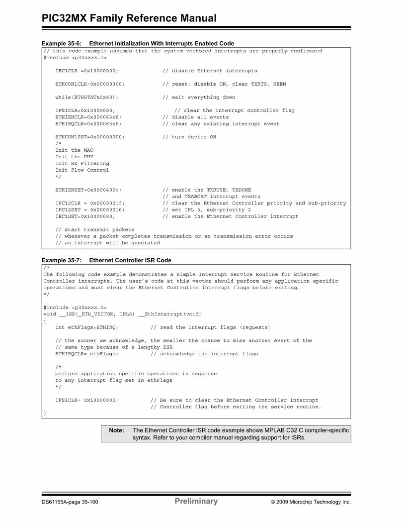
PIC32MX Family Reference Manual
Example 35-6: Ethernet Initialization With Interrupts Enabled Code
Example 35-7: Ethernet Controller ISR Code
// this code example assumes that the system vectored interrupts are properly configured#include <p32xxxx.h>
IEC1CLR =0x10000000; // disable Ethernet interrupts
ETHCON1CLR=0x00008300; // reset: disable ON, clear TXRTS, RXEN
while(ETHSTAT&0x80); // wait everything down
IFS1CLR=0x10000000; // clear the interrupt controller flagETHIENCLR=0x000063ef; // disable all eventsETHIRQCLR=0x000063ef; // clear any existing interrupt event
ETHCON1SET=0x00008000; // turn device ON/*Init the MACInit the PHYInit RX FilteringInit Flow Control*/
ETHIENSET=0x0000400c; // enable the TXBUSE, TXDONE// and TXABORT interrupt events
IPC12CLR = 0x0000001f; // clear the Ethernet Controller priority and sub-priorityIPC12SET = 0x00000016; // set IPL 5, sub-priority 2IEC1SET=0x10000000; // enable the Ethernet Controller interrupt
// start transmit packets// whenever a packet completes transmission or an transmission error occurs// an interrupt will be generated
/*The following code example demonstrates a simple Interrupt Service Routine for Ethernet Controller interrupts. The user’s code at this vector should perform any application specific operations and must clear the Ethernet Controller interrupt flags before exiting.*/
#include <p32xxxx.h>void __ISR(_ETH_VECTOR, IPL5) __EthInterrupt(void){
int ethFlags=ETHIRQ; // read the interrupt flags (requests)
// the sooner we acknowledge, the smaller the chance to miss another event of the// same type because of a lengthy ISRETHIRQCLR= ethFlags; // acknowledge the interrupt flags
/*perform application specific operations in responseto any interrupt flag set in ethFlags*/
IFS1CLR= 0x10000000; // Be sure to clear the Ethernet Controller Interrupt// Controller flag before exiting the service routine.
}
Note: The Ethernet Controller ISR code example shows MPLAB C32 C compiler-specificsyntax. Refer to your compiler manual regarding support for ISRs.
DS61155A-page 35-100 Preliminary © 2009 Microchip Technology Inc.

Section 35. Ethernet ControllerEthernet
Controller
35
35.5.2 External PHY InterruptSome PHYs have the option of generating an interrupt signal when a specific event occurs. APHY interrupt is usually asserted for the following types of events/conditions:
• Energy Detect• Power-Down mode exited• Auto-negotiation complete• Remote fault detected• Link down• Auto-negotiation LP acknowledge• Parallel detection fault• Auto-negotiation page received
Refer the vendor-specific PHY data sheet for the details about the events generating interrupts.
If the PIC32MX has to be made aware and respond to this interrupt, then the PHY interrupt signalshould be tied to a PIC32MX external interrupt pin. Note that this interrupt does not go throughthe Ethernet Controller.
The software has to clear the PHY generated interrupt event by writing a register in the PHY viathe MAC MIIM registers. Note that in this case, the PHY interrupt is the only software-clearableinterrupt that is not directly clearable in the ETHIRQ register.
© 2009 Microchip Technology Inc. Preliminary DS61155A-page 35-101
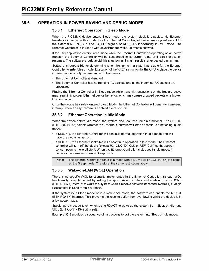
PIC32MX Family Reference Manual
35.6 OPERATION IN POWER-SAVING AND DEBUG MODES
35.6.1 Ethernet Operation in Sleep ModeWhen the PIC32MX device enters Sleep mode, the system clock is disabled. No Ethernettransfers can occur in this mode. For the Ethernet Controller, all clocks are stopped except forthe external MII RX_CLK and TX_CLK signals or REF_CLK if operating in RMII mode. TheEthernet Controller is in Sleep with asynchronous wake-up events allowed.
If the user application enters Sleep mode while the Ethernet Controller is operating on an activetransfer, the Ethernet Controller will be suspended in its current state until clock executionresumes. The software should avoid this situation as it might result in unexpected pin timings.
Software is responsible for determining when the link is in a state that is safe for the EthernetController to enter Sleep mode. Execution of the WAIT instruction by the CPU to place the devicein Sleep mode is only recommended in two cases:
• The Ethernet Controller is disabled.• The Ethernet Controller has no pending TX packets and all the incoming RX packets are
processed.
Placing the Ethernet Controller in Sleep mode while transmit transactions on the bus are activemay result in improper Ethernet device behavior, which may cause dropped packets or a brokenlink connection.
Once the device has safely entered Sleep Mode, the Ethernet Controller will generate a wake-upinterrupt when an asynchronous enabled event occurs.
35.6.2 Ethernet Operation in Idle ModeWhen the device enters Idle mode, the system clock sources remain functional. The SIDL bit(ETHCON1<13>) selects whether the Ethernet Controller will stop or continue functioning in Idlemode:
• If SIDL = 0, the Ethernet Controller will continue normal operation in Idle mode and will have the clocks turned on.
• If SIDL = 1, the Ethernet Controller will discontinue operation in Idle mode. The Ethernet controller will turn off the clocks (except RX_CLK, TX_CLK or REF_CLK) so that power consumption is more efficient. When the Ethernet Controller is stopped in Idle mode, it behaves the same as when in Sleep mode.
35.6.3 Wake-on-LAN (WOL) OperationThere is no specific WOL functionality implemented in the Ethernet Controller. Instead, WOLfunctionality is implemented by setting the appropriate RX filters and enabling the RXDONE(ETHIRQ<7>) interrupt to wake this system when a receive packet is accepted. Normally a MagicPacket filter is used for this purpose.
If the system is in Sleep mode or in a slow-clock mode, the software can enable the RXACT(ETHIRQ<5>) interrupt. This prevents the receive buffer from overflowing while the device is ina low power mode.
Special care must be taken when using RXACT to wake-up the system from Sleep or Idle (andSIDL (ETHCON1<13>) bit is set).
Example 35-8 provides a sequence of instructions to put the system into Sleep or Idle mode.
Note: The Ethernet Controller treats Idle mode with SIDL = 1 (ETHCON1<13>) the sameas the Sleep mode. Therefore, the same restrictions apply.
DS61155A-page 35-102 Preliminary © 2009 Microchip Technology Inc.

Section 35. Ethernet ControllerEthernet
Controller
35
Example 35-8: Using the Ethernet Controller to Wake-up the System
Under these circumstances, the wake-up ISR should look like Example 35-9:
Example 35-9: Ethernet Controller Wake-up on RXACT ISR
/*The following code example illustrates a simple sequence of instructions to put the system into Sleep or Idle state so that the incoming Ethernet activity, signaled by RXACT, is used to wake-up the system. It assumes that either the Sleep state is enabled or, if the Idle state is enabled, the Ethernet Controller SIDL bit is set.*/#include <p32xxxx.h>
if(want_to_sleep){
ETHIRQCLR = 0x20; // clear RXACT flagETHIENSET = 0x20; // enable RXACT interruptasm(“wait”); // go to Sleep/Idle
}
/*The following code example demonstrates a simple Interrupt Service Routine for Ethernet Controller interrupts. The user’s code at this vector should perform any application specific operations and must clear the Ethernet Controller interrupt flags before exiting.*/#include <p32xxxx.h>
void __ISR(_ETH_VECTOR, IPL5) __EthInterrupt(void){int ethFlags=ETHIRQ; // read the interrupt flags (requests)
ethFlags =ETHIRQ;if(ethFlags &0x20){ // RXACT interrupt
ETHIENCLR = 0x20; // disable further RXACT interruptsETHCON1CLR= 0x2000; // disable SIDL
// suspend any activity in your system that could interfere// with the critical system unlock sequence such as:// disable higher priority interrupts, DMA transfers, etc.// now unlock the system
SYSKEY = 0, SYSKEY = 0xAA996655, SYSKEY = 0x556699AA;OSCCONCLR = 0x10; // disable SLEEP mode, enable IDLESYSKEY = 0x33333333; // relock the system
// resume the activity previously stopped: re-enable interrupts,// DMA, etc.
}
/*perform other application specific operations in responseto other interrupt flag set in ethFlags*/
ETHIRQCLR= ethFlags; // acknowledge the interrupt flags
IFS1CLR= 0x10000000; // clear the Ethernet Controller Interrupt Controller// flag before exiting the service routine.
}
Note: The Ethernet Controller ISR code example shows MPLAB C32 C compiler-specificsyntax. Refer to your compiler manual regarding support for ISRs.
© 2009 Microchip Technology Inc. Preliminary DS61155A-page 35-103
PIC32MX Family Reference Manual
The disabling of further RXACT interrupts in this ISR is needed because of the way the EthernetController generates this interrupt request, which is active as long as there is data in the RXFIFO. Otherwise, the control will continuously get back to the ISR and execution will be lockedup.
However, instead of simply disabling the RXACT interrupt, further action is needed: disable theSleep mode and enable the Idle mode and make sure that the Ethernet Controller is enabled(SIDL = 0). This is needed to prevent the situation where a RXACT interrupt was taken exactlyafter the enabling of the RXACT, but just before the execution of the WAIT instruction in the mainloop of Example 35-9.
If activity was received right before the WAIT instruction call, the ISR will disable the RX activityinterrupt and when the ISR returns the main loop will execute the WAIT instruction. At this point,the Ethernet Controller will never be able to wake the part.
The workaround is to have the ISR disable Sleep mode and clear the Ethernet SIDL bits so thatthe Ethernet Controller will not go to sleep.
Please note that another Ethernet interrupt needs to be enabled after the RXACT interrupt isdisabled. Usually, the RXDONE bit is the best candidate.
35.6.4 Ethernet Operation in Debug ModeThe FRZ (ETHCON1<14>) bit determines whether the Ethernet Controller will run or stop whilethe CPU is executing debug exception code (i.e., application is halted) in Debug mode.
• When FRZ = 0, the Ethernet Controller continues to run even when the application is halted in Debug mode.
• When FRZ = 1 and the application is halted in Debug mode, the Ethernet Controller will complete the current bus transaction, and will then freeze its operations and make no changes to the state of the Ethernet Controller. All Ethernet Controller registers are readable and writable; however, reads are non-destructive and do not alter the state of the peripheral. System clocks to the rest of the peripheral are stopped except for the external RX_CLK /TX_CLK (MII) or REF_CLK (RMII) clocks. The peripheral will resume its operation after the CPU resumes execution.
Note: The FRZ bit is readable and writable only when the CPU is executing in DebugException mode. In all other modes, the FRZ bit reads as ‘0’. If the FRZ bit ischanged during Debug mode, the new value does not take effect until the currentDebug Exception mode is exited and re-entered. During the Debug Exceptionmode, the FRZ bit reads the state of the peripheral when entering Debug mode.When the Ethernet peripheral is frozen, it is unable to follow normal Ethernet proto-col. This means that transmit frames may be aborted and receive frames may bedropped.
DS61155A-page 35-104 Preliminary © 2009 Microchip Technology Inc.

Section 35. Ethernet ControllerEthernet
Controller
35
35.7 EFFECTS OF VARIOUS RESETS
35.7.1 Device ResetAll Ethernet registers are forced to their reset states upon a device Reset. When theasynchronous reset input goes active, the Ethernet logic does the following:
• Resets all fields in the SFRs (ETHCON1, ETHCON2, ETHSTAT, etc.).• Loads the EMACxSA0, EMACxSA1 and EMACxSA2 registers containing the station
address from the factory pre-programmed station address.• Resets the TX and RX DMA engines, and puts the corresponding FIFOs in the empty state.• Aborts any on-going data transfers.
35.7.2 Power-on ResetAll Ethernet Controller registers are forced to their reset states upon a Power-on Reset.
35.7.3 Watchdog Timer ResetAll Ethernet Controller registers are forced to their reset states upon a Watchdog Timer Reset.
© 2009 Microchip Technology Inc. Preliminary DS61155A-page 35-105

PIC32MX Family Reference Manual
35.8 I/O PIN CONTROLEnabling the Ethernet Controller will configure the I/O pin direction as defined by the EthernetController control bits (see Table 35-10). The port TRIS and LATCH registers will be overridden.
Table 35-10: I/O Pin Configuration for Use with the Ethernet Controller
I/O Pin Name
MII Required
RMII Required
Module Control TRIS(1) Pin Type Description
EMDC Yes Yes ON X O Ethernet MII Management ClockEMDIO Yes Yes ON X I/O Ethernet MII Management IOETXCLK Yes No ON X I Ethernet MII TX ClockETXEN Yes Yes ON X O Ethernet Transmit EnableETXD0 Yes Yes ON X O Ethernet Data Transmit 0ETXD1 Yes Yes ON X O Ethernet Data Transmit 1ETXD2 Yes No ON X O Ethernet Data Transmit 2ETXD3 Yes No ON X O Ethernet Data Transmit 3ETXERR Yes No ON X O Ethernet Transmit ErrorERXCLK Yes No ON X I Ethernet MII RX ClockEREF_CLK No Yes ON X I Ethernet RMII Ref ClockERXDV Yes No ON X I Ethernet MII Receive Data ValidECRS_DV No Yes ON X I Ethernet RMII Carrier Sense/Receive Data ValidERXD0 Yes Yes ON X I Ethernet Data Receive 0ERXD1 Yes Yes ON X I Ethernet Data Receive 1ERXD2 Yes No ON X I Ethernet Data Receive 2ERXD3 Yes No ON X I Ethernet Data Receive 3ERXERR Yes Yes ON X I Ethernet Receive ErrorECRS Yes No ON X I Ethernet Carrier SenseECOL Yes No ON X I Ethernet Collision DetectedNote 1: The setting of the TRIS bit is irrelevant. However, If the pin is shared with an analog input, the AD1PCFG
and corresponding TRIS register must be properly set to configure this pin as digital.
DS61155A-page 35-106 Preliminary © 2009 Microchip Technology Inc.
Section 35. Ethernet ControllerEthernet
Controller
35
35.9 RELATED APPLICATION NOTESThis section lists application notes that are related to this section of the manual. Theseapplication notes may not be written specifically for the PIC32MX device family, but the conceptsare pertinent and could be used with modification and possible limitations. The currentapplication notes related to the Ethernet Controller module are:
Title Application Note #Ethernet Theory of Operation AN1120
Note: Please visit the Microchip web site (www.microchip.com) for additional ApplicationNotes and code examples for the PIC32MX family of devices.
© 2009 Microchip Technology Inc. Preliminary DS61155A-page 35-107
PIC32MX Family Reference Manual
35.10 REVISION HISTORY
Revision A (August 2009)
This is the initial released version of this document.
DS61155A-page 35-108 Preliminary © 2009 Microchip Technology Inc.