PIC24F Family Ref. Manual, Section 52. Liquid Crystal Display (LCD) · · 2013-06-08Section 52....
44
© 2010 Microchip Technology Inc. DS39740A-page 52-1 Liquid Crystal Display (LCD) 52 Section 52. Liquid Crystal Display (LCD) HIGHLIGHTS This section of the manual contains the following major topics: 52.1 Introduction .................................................................................................................. 52-2 52.2 LCD Registers.............................................................................................................. 52-3 52.3 LCD Segment Pins Configuration ................................................................................ 52-6 52.4 LCD Clock Source Selection........................................................................................ 52-8 52.5 LCD Bias Types ........................................................................................................... 52-9 52.6 LCD Multiplex Types .................................................................................................. 52-21 52.7 Segment Enables....................................................................................................... 52-22 52.8 Pixel Control............................................................................................................... 52-22 52.9 LCD Frame Frequency .............................................................................................. 52-22 52.10 LCD Waveform Generation........................................................................................ 52-22 52.11 LCD Interrupts............................................................................................................ 52-36 52.12 Configuring the LCD Module...................................................................................... 52-38 52.13 Operation During Sleep ............................................................................................. 52-39 52.14 Registers .................................................................................................................... 52-40 52.15 Revision History ......................................................................................................... 52-41
Transcript of PIC24F Family Ref. Manual, Section 52. Liquid Crystal Display (LCD) · · 2013-06-08Section 52....
Section 52. Liquid Crystal Display (LCD)
Liq
uid
Crystal
Disp
lay (LC
D)
52
HIGHLIGHTS
This section of the manual contains the following major topics:
52.1 Introduction .................................................................................................................. 52-2
52.2 LCD Registers.............................................................................................................. 52-3
52.3 LCD Segment Pins Configuration ................................................................................ 52-6
52.4 LCD Clock Source Selection........................................................................................ 52-8
52.5 LCD Bias Types ........................................................................................................... 52-9
52.6 LCD Multiplex Types .................................................................................................. 52-21
52.7 Segment Enables....................................................................................................... 52-22
52.8 Pixel Control............................................................................................................... 52-22
52.9 LCD Frame Frequency .............................................................................................. 52-22
52.10 LCD Waveform Generation........................................................................................ 52-22
52.11 LCD Interrupts............................................................................................................ 52-36
52.12 Configuring the LCD Module...................................................................................... 52-38
52.13 Operation During Sleep ............................................................................................. 52-39
52.14 Registers.................................................................................................................... 52-40
52.15 Revision History ......................................................................................................... 52-41
© 2010 Microchip Technology Inc. DS39740A-page 52-1
PIC24F Family Reference Manual
52.1 INTRODUCTION
The Liquid Crystal Display (LCD) driver module generates the timing control to drive a static ormultiplexed LCD panel. In the 100-pin devices (PIC24FJXXXGA3XX), the module drives panelsof up to eight commons and up to 60 segments when 5 to 8 commons are used, and up to64 segments when 1 to 4 commons are used. It also provides control of the LCD pixel data.
The LCD driver module supports:
• Direct driving of LCD panel
• Three LCD clock sources with selectable prescaler
• Up to eight commons:
- Static (one common)
- 1/2 Multiplex (two commons)
- 1/3 Multiplex (three commons)
- 1/8 Multiplex (eight commons)
• Up to 60 segments (in 100-pin devices when 1/5-1/8 Multiplex is selected), 64 (in 100-pin devices when up to 1/4 Multiplex is selected), 46 (in 80-pin devices when 1/5-1/8 Multiplex is selected), 50 (in 80-pin devices when up to 1/4 Multiplex is selected), 30 (in 64-pin devices when 1/5-1/8 Multiplex is selected) and 34 (in 64-pin devices when up to 1/4 Multiplex is selected)
• Static, 1/2 or 1/3 LCD Bias
• On-chip Bias generator with dedicated charge pump to support a range of fixed and variable Bias options
• Internal resistors for Bias voltage generation
• Software contrast control for LCD using the internal biasing
A simplified block diagram of the module is shown in Figure 52-1.
Figure 52-1: LCD Driver Module Block Diagram
COM<7:0>
Timing Control
Data Bus
SOSC
FRC OscillatorLPRC Oscillator
512
to
64
MUXSEG<63:0>
To I/O Pins
32 x 16 (= 8x 64)LCD DATA
LCDCON
LCDPS
LCDSEx
LCDDATA0
LCDDATA1
LCDDATA30
LCDDATA31
...
LCD Bias Generation
LCD Clock
Source SelectLCD
Charge Pump
64
8
BiasVoltage
16
(Secondary Oscillator)
Resistor Ladder
DS39740A-page 52-2 © 2010 Microchip Technology Inc.
Section 52. Liquid Crystal Display (LCD)L
iqu
id C
rystalD
isplay (L
CD
)
52
52.2 LCD REGISTERS
The LCD driver module has 40 registers:
• LCD Control Register (LCDCON)
• LCD Phase Register (LCDPS)
• LCD Voltage Regulator Control Register (LCDREG)
• LCD Reference Ladder Control Register (LCDREF)
• Four LCD Segment Enable Registers (LCDSE3:LCDSE0)
• 32 LCD Data Registers (LCDDATA31:LCDDATA0)
The LCDCON register, shown in Register 52-1, controls the overall operation of the module. Oncethe module is configured, the LCDEN (LCDCON<15>) bit is used to enable or disable the LCDmodule. The LCD panel can also operate during Sleep by clearing the SLPEN (LCDCON<6>) bit.
The LCDPS register, shown in Register 52-2, configures the LCD clock source prescaler and thetype of waveform: Type-A or Type-B. For details on these features, see Section 52.4 “LCDClock Source Selection”, Section Table 52-6: “Special Function Registers Associated withLCD Driver Module” and Section 52.10 “LCD Waveform Generation”.
Register 52-1: LCDCON: LCD Control Register
R/W-0 U-0 R/W-0 U-0 U-0 U-0 U-0 U-0
LCDEN — LCDSIDL — — — — —
bit 15 bit 8
U-0 R/W-0 R/C-0 R/W-0 R/W-0 R/W-0 R/W-0 R/W-0
— SLPEN WERR CS1 CS0 LMUX2 LMUX1 LMUX0
bit 7 bit 0
Legend: C = Clearable bit
R = Readable bit W = Writable bit U = Unimplemented bit, read as ‘0’
-n = Value at POR ‘1’ = Bit is set ‘0’ = Bit is cleared x = Bit is unknown
bit 15 LCDEN: LCD Driver Enable bit
1 = LCD driver module is enabled0 = LCD driver module is disabled
bit 14 Unimplemented: Read as ‘0’
bit 13 LCDSIDL: Stop LCD Drive in CPU Idle mode control bit
1 = LCD driver halts in CPU Idle mode0 = LCD driver continues to operate in CPU Idle mode
bit 12-7 Unimplemented: Read as '0'
bit 6 SLPEN: LCD Driver Enable in Sleep Mode bit
1 = LCD driver module is disabled in Sleep mode0 = LCD driver module is enabled in Sleep mode
bit 5 WERR: LCD Write Failed Error bit
1 = LCDDATAx register is written while WA (LCDPS<4>) = 0 (must be cleared in software)0 = No LCD write error
bit 4-3 CS<1:0>: Clock Source Select bits
00 = FRC (8 MHz)/819201 = SOSC oscillator (32.768 kHz)/321x = INTRC (31.25 kHz)/32
© 2010 Microchip Technology Inc. DS39740A-page 52-3
PIC24F Family Reference Manual
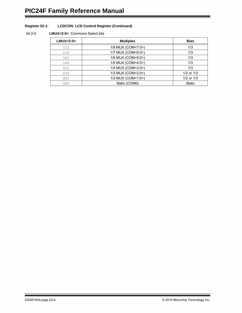
bit 2-0 LMUX<2:0>: Commons Select bits
Register 52-1: LCDCON: LCD Control Register (Continued)
LMUX<2:0> Multiplex Bias
111 1/8 MUX (COM<7:0>) 1/3
110 1/7 MUX (COM<6:0>) 1/3
101 1/6 MUX (COM<5:0>) 1/3
100 1/5 MUX (COM<4:0>) 1/3
011 1/4 MUX (COM<3:0>) 1/3
010 1/3 MUX (COM<2:0>) 1/2 or 1/3
001 1/2 MUX (COM<1:0>) 1/2 or 1/3
000 Static (COM0) Static
DS39740A-page 52-4 © 2010 Microchip Technology Inc.
Section 52. Liquid Crystal Display (LCD)L
iqu
id C
rystalD
isplay (L
CD
)
52
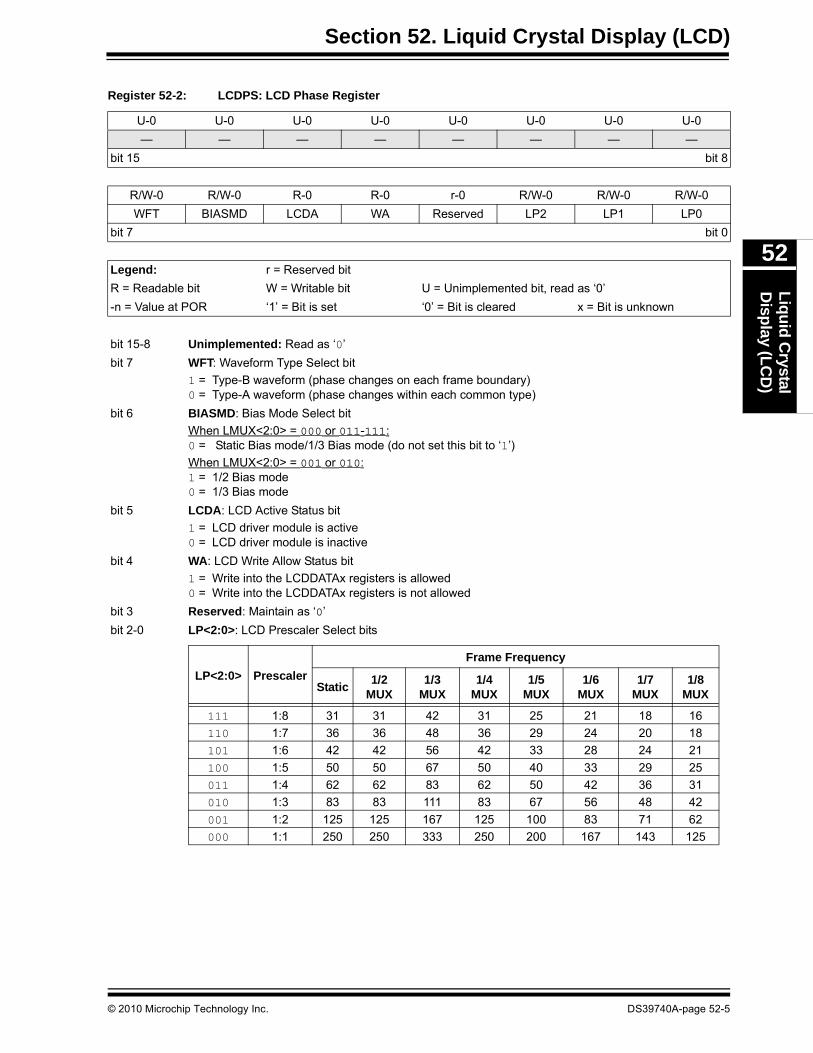
Register 52-2: LCDPS: LCD Phase Register
U-0 U-0 U-0 U-0 U-0 U-0 U-0 U-0
— — — — — — — —
bit 15 bit 8
R/W-0 R/W-0 R-0 R-0 r-0 R/W-0 R/W-0 R/W-0
WFT BIASMD LCDA WA Reserved LP2 LP1 LP0
bit 7 bit 0
Legend: r = Reserved bit
R = Readable bit W = Writable bit U = Unimplemented bit, read as ‘0’
-n = Value at POR ‘1’ = Bit is set ‘0’ = Bit is cleared x = Bit is unknown
bit 15-8 Unimplemented: Read as ‘0’
bit 7 WFT: Waveform Type Select bit
1 = Type-B waveform (phase changes on each frame boundary)0 = Type-A waveform (phase changes within each common type)
bit 6 BIASMD: Bias Mode Select bit
When LMUX<2:0> = 000 or 011-111:0 = Static Bias mode/1/3 Bias mode (do not set this bit to ‘1’)
When LMUX<2:0> = 001 or 010:1 = 1/2 Bias mode0 = 1/3 Bias mode
bit 5 LCDA: LCD Active Status bit
1 = LCD driver module is active0 = LCD driver module is inactive
bit 4 WA: LCD Write Allow Status bit
1 = Write into the LCDDATAx registers is allowed0 = Write into the LCDDATAx registers is not allowed
bit 3 Reserved: Maintain as ‘0’
bit 2-0 LP<2:0>: LCD Prescaler Select bits
LP<2:0> Prescaler
Frame Frequency
Static1/2
MUX1/3
MUX1/4
MUX1/5
MUX1/6
MUX1/7
MUX1/8
MUX
111 1:8 31 31 42 31 25 21 18 16
110 1:7 36 36 48 36 29 24 20 18
101 1:6 42 42 56 42 33 28 24 21
100 1:5 50 50 67 50 40 33 29 25
011 1:4 62 62 83 62 50 42 36 31
010 1:3 83 83 111 83 67 56 48 42
001 1:2 125 125 167 125 100 83 71 62
000 1:1 250 250 333 250 200 167 143 125
© 2010 Microchip Technology Inc. DS39740A-page 52-5
PIC24F Family Reference Manual
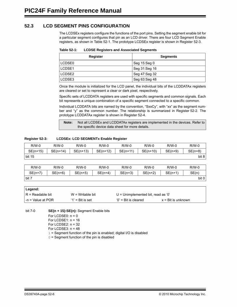
52.3 LCD SEGMENT PINS CONFIGURATION
The LCDSEx registers configure the functions of the port pins. Setting the segment enable bit fora particular segment configures that pin as an LCD driver. There are four LCD Segment Enableregisters, as shown in Table 52-1. The prototype LCDSEx register is shown in Register 52-3.
Once the module is initialized for the LCD panel, the individual bits of the LCDDATAx registersare cleared or set to represent a clear or dark pixel, respectively.
Specific sets of LCDDATA registers are used with specific segments and common signals. Eachbit represents a unique combination of a specific segment connected to a specific common.
Individual LCDDATA bits are named by the convention, “SxxCy”, with “xx” as the segment num-ber and “y” as the common number. The relationship is summarized in Register 52-2. Theprototype LCDDATAx register is shown in Register 52-4.
Register 52-3: LCDSEx: LCD SEGMENTx Enable Register
Table 52-1: LCDSE Registers and Associated Segments
Register Segments
LCDSE0 Seg 15:Seg 0
LCDSE1 Seg 31:Seg 16
LCDSE2 Seg 47:Seg 32
LCDSE3 Seg 63:Seg 48
Note: Not all LCDSEx and LCDDATAx registers are implemented in the devices. Refer tothe specific device data sheet for more details.
R/W-0 R/W-0 R/W-0 R/W-0 R/W-0 R/W-0 R/W-0 R/W-0
SE(n+15) SE(n+14) SE(n+13) SE(n+12) SE(n+11) SE(n+10) SE(n+9) SE(n+8)
bit 15 bit 8
R/W-0 R/W-0 R/W-0 R/W-0 R/W-0 R/W-0 R/W-0 R/W-0
SE(n+7) SE(n+6) SE(n+5) SE(n+4) SE(n+3) SE(n+2) SE(n+1) SE(n)
bit 7 bit 0
Legend:
R = Readable bit W = Writable bit U = Unimplemented bit, read as ‘0’
-n = Value at POR ‘1’ = Bit is set ‘0’ = Bit is cleared x = Bit is unknown
bit 7-0 SE(n + 15):SE(n): Segment Enable bits
For LCDSE0: n = 0For LCDSE1: n = 16For LCDSE2: n = 32For LCDSE3: n = 481 = Segment function of the pin is enabled; digital I/O is disabled0 = Segment function of the pin is disabled
DS39740A-page 52-6 © 2010 Microchip Technology Inc.
Section 52. Liquid Crystal Display (LCD)L
iqu
id C
rystalD
isplay (L
CD
)
52
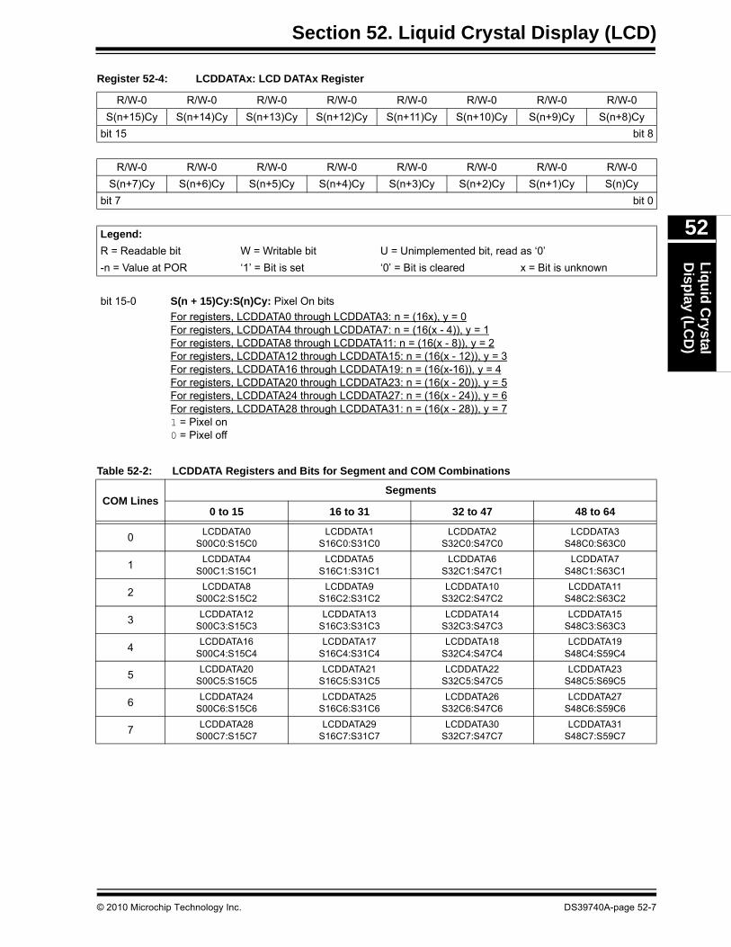
Register 52-4: LCDDATAx: LCD DATAx Register
Table 52-2: LCDDATA Registers and Bits for Segment and COM Combinations
R/W-0 R/W-0 R/W-0 R/W-0 R/W-0 R/W-0 R/W-0 R/W-0
S(n+15)Cy S(n+14)Cy S(n+13)Cy S(n+12)Cy S(n+11)Cy S(n+10)Cy S(n+9)Cy S(n+8)Cy
bit 15 bit 8
R/W-0 R/W-0 R/W-0 R/W-0 R/W-0 R/W-0 R/W-0 R/W-0
S(n+7)Cy S(n+6)Cy S(n+5)Cy S(n+4)Cy S(n+3)Cy S(n+2)Cy S(n+1)Cy S(n)Cy
bit 7 bit 0
Legend:
R = Readable bit W = Writable bit U = Unimplemented bit, read as ‘0’
-n = Value at POR ‘1’ = Bit is set ‘0’ = Bit is cleared x = Bit is unknown
bit 15-0 S(n + 15)Cy:S(n)Cy: Pixel On bits
For registers, LCDDATA0 through LCDDATA3: n = (16x), y = 0For registers, LCDDATA4 through LCDDATA7: n = (16(x - 4)), y = 1For registers, LCDDATA8 through LCDDATA11: n = (16(x - 8)), y = 2For registers, LCDDATA12 through LCDDATA15: n = (16(x - 12)), y = 3For registers, LCDDATA16 through LCDDATA19: n = (16(x-16)), y = 4For registers, LCDDATA20 through LCDDATA23: n = (16(x - 20)), y = 5For registers, LCDDATA24 through LCDDATA27: n = (16(x - 24)), y = 6For registers, LCDDATA28 through LCDDATA31: n = (16(x - 28)), y = 71 = Pixel on 0 = Pixel off
COM LinesSegments
0 to 15 16 to 31 32 to 47 48 to 64
0LCDDATA0
S00C0:S15C0LCDDATA1
S16C0:S31C0LCDDATA2
S32C0:S47C0LCDDATA3
S48C0:S63C0
1LCDDATA4
S00C1:S15C1LCDDATA5
S16C1:S31C1LCDDATA6
S32C1:S47C1LCDDATA7
S48C1:S63C1
2LCDDATA8
S00C2:S15C2LCDDATA9
S16C2:S31C2LCDDATA10
S32C2:S47C2LCDDATA11
S48C2:S63C2
3LCDDATA12
S00C3:S15C3LCDDATA13
S16C3:S31C3LCDDATA14
S32C3:S47C3LCDDATA15
S48C3:S63C3
4LCDDATA16
S00C4:S15C4LCDDATA17
S16C4:S31C4LCDDATA18
S32C4:S47C4LCDDATA19
S48C4:S59C4
5LCDDATA20
S00C5:S15C5LCDDATA21
S16C5:S31C5LCDDATA22
S32C5:S47C5LCDDATA23
S48C5:S69C5
6LCDDATA24
S00C6:S15C6LCDDATA25
S16C6:S31C6LCDDATA26
S32C6:S47C6LCDDATA27
S48C6:S59C6
7LCDDATA28
S00C7:S15C7LCDDATA29
S16C7:S31C7LCDDATA30
S32C7:S47C7LCDDATA31
S48C7:S59C7
© 2010 Microchip Technology Inc. DS39740A-page 52-7
PIC24F Family Reference Manual
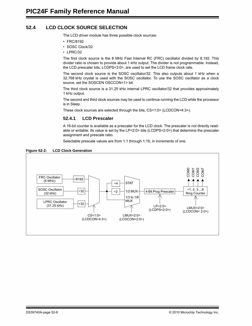
52.4 LCD CLOCK SOURCE SELECTION
The LCD driver module has three possible clock sources:
• FRC/8192
• SOSC Clock/32
• LPRC/32
The first clock source is the 8 MHz Fast Internal RC (FRC) oscillator divided by 8,192. Thisdivider ratio is chosen to provide about 1 kHz output. The divider is not programmable. Instead,the LCD prescaler bits, LCDPS<3:0>, are used to set the LCD frame clock rate.
The second clock source is the SOSC oscillator/32. This also outputs about 1 kHz when a32.768 kHz crystal is used with the SOSC oscillator. To use the SOSC oscillator as a clocksource, set the SOSCEN OSCCON<1> bit.
The third clock source is a 31.25 kHz internal LPRC oscillator/32 that provides approximately1 kHz output.
The second and third clock sources may be used to continue running the LCD while the processoris in Sleep.
These clock sources are selected through the bits, CS<1:0> (LCDCON<4:3>).
52.4.1 LCD Prescaler
A 16-bit counter is available as a prescaler for the LCD clock. The prescaler is not directly read-able or writable. Its value is set by the LP<2:0> bits (LCDPS<2:0>) that determine the prescalerassignment and prescale ratio.
Selectable prescale values are from 1:1 through 1:16, in increments of one.
Figure 52-2: LCD Clock Generation
CS<1:0>
SOSC Oscillator(32 kHz)
LPRC Oscillator(31.25 kHz)
STAT
1/2 MUX
1/3 to 1/8MUX
÷4
LMUX<2:0>
4-Bit Prog Prescaler÷1, 2, 3....8
Ring Counter
LMUX<2:0>
CO
M0
CO
M1
CO
M2
CO
M7
÷8192(8 MHZ)
÷2÷32
÷32LP<2:0>
(LCDCON<4:3>) (LCDCON<2:0>)
(LCDCON< 2:0>)(LCDPS<2:0>)
FRC Oscillator
DS39740A-page 52-8 © 2010 Microchip Technology Inc.
Section 52. Liquid Crystal Display (LCD)L
iqu
id C
rystalD
isplay (L
CD
)
52
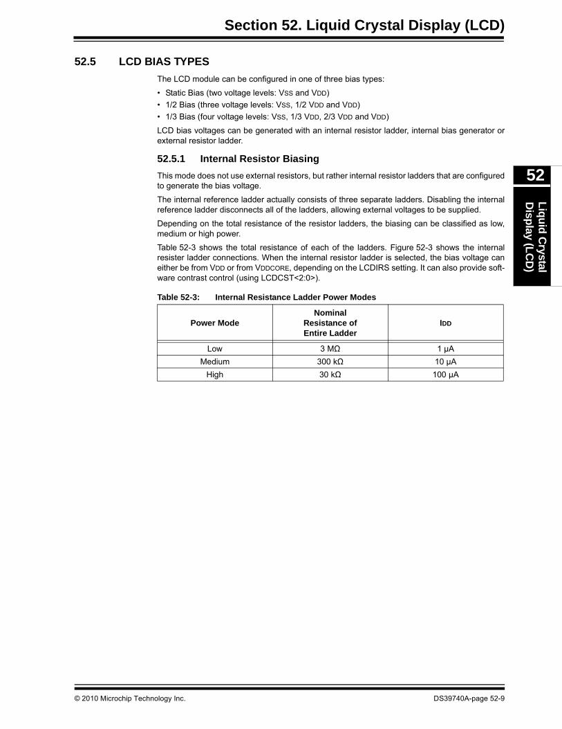
52.5 LCD BIAS TYPES
The LCD module can be configured in one of three bias types:
• Static Bias (two voltage levels: VSS and VDD)
• 1/2 Bias (three voltage levels: VSS, 1/2 VDD and VDD)
• 1/3 Bias (four voltage levels: VSS, 1/3 VDD, 2/3 VDD and VDD)
LCD bias voltages can be generated with an internal resistor ladder, internal bias generator orexternal resistor ladder.
52.5.1 Internal Resistor Biasing
This mode does not use external resistors, but rather internal resistor ladders that are configuredto generate the bias voltage.
The internal reference ladder actually consists of three separate ladders. Disabling the internalreference ladder disconnects all of the ladders, allowing external voltages to be supplied.
Depending on the total resistance of the resistor ladders, the biasing can be classified as low,medium or high power.
Table 52-3 shows the total resistance of each of the ladders. Figure 52-3 shows the internalresister ladder connections. When the internal resistor ladder is selected, the bias voltage caneither be from VDD or from VDDCORE, depending on the LCDIRS setting. It can also provide soft-ware contrast control (using LCDCST<2:0>).
Table 52-3: Internal Resistance Ladder Power Modes
Power ModeNominal
Resistance ofEntire Ladder
IDD
Low 3 MΩ 1 µA
Medium 300 kΩ 10 µA
High 30 kΩ 100 µA
© 2010 Microchip Technology Inc. DS39740A-page 52-9
PIC24F Family Reference Manual
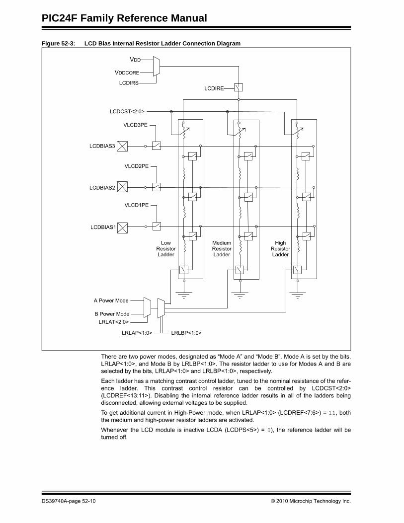
Figure 52-3: LCD Bias Internal Resistor Ladder Connection Diagram
There are two power modes, designated as “Mode A” and “Mode B”. Mode A is set by the bits,LRLAP<1:0>, and Mode B by LRLBP<1:0>. The resistor ladder to use for Modes A and B areselected by the bits, LRLAP<1:0> and LRLBP<1:0>, respectively.
Each ladder has a matching contrast control ladder, tuned to the nominal resistance of the refer-ence ladder. This contrast control resistor can be controlled by LCDCST<2:0>(LCDREF<13:11>). Disabling the internal reference ladder results in all of the ladders beingdisconnected, allowing external voltages to be supplied.
To get additional current in High-Power mode, when LRLAP<1:0> (LCDREF<7:6>) = 11, boththe medium and high-power resistor ladders are activated.
Whenever the LCD module is inactive LCDA (LCDPS<5>) = 0), the reference ladder will beturned off.
LCDBIAS3
LCDBIAS2
LCDBIAS1
VLCD3PE
VLCD2PE
VLCD1PE
LCDCST<2:0>
LCDIRELCDIRS
VDD
3x Band Gap
LRLAT<2:0>
A Power Mode
B Power Mode
LRLAP<1:0> LRLBP<1:0>
LowResistorLadder
MediumResistorLadder
HighResistorLadder
VDD
VDDCORE
DS39740A-page 52-10 © 2010 Microchip Technology Inc.
Section 52. Liquid Crystal Display (LCD)L
iqu
id C
rystalD
isplay (L
CD
)
52
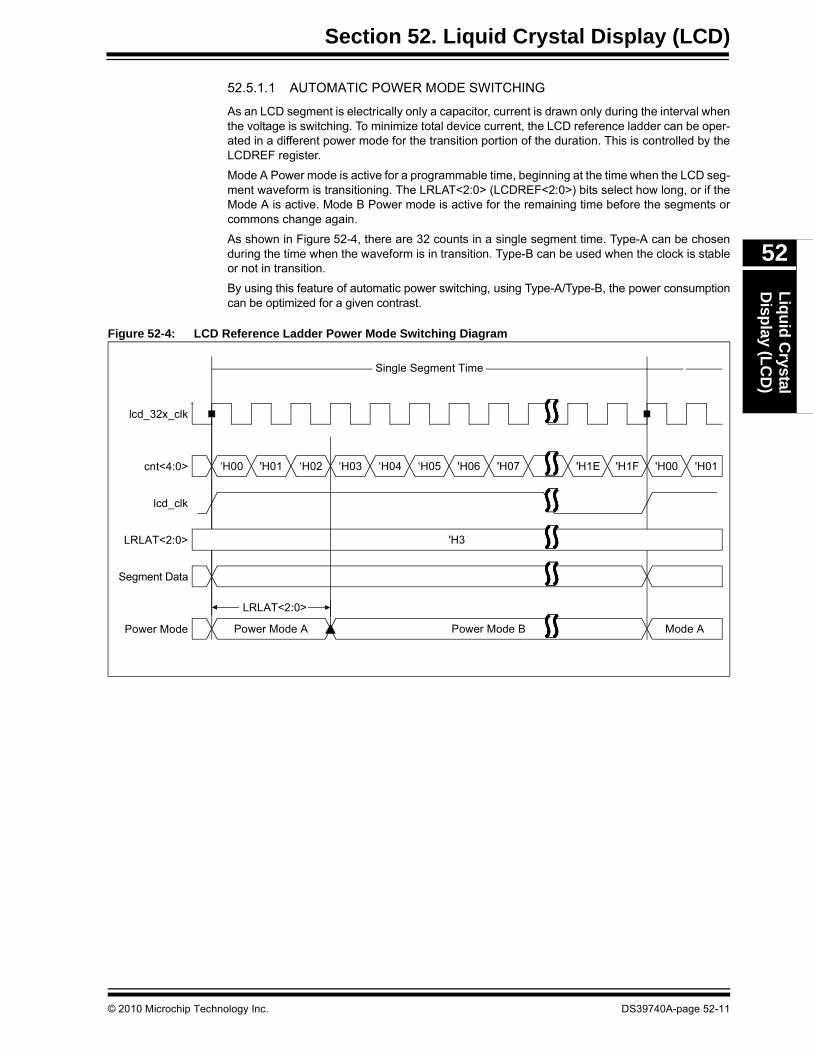
52.5.1.1 AUTOMATIC POWER MODE SWITCHING
As an LCD segment is electrically only a capacitor, current is drawn only during the interval whenthe voltage is switching. To minimize total device current, the LCD reference ladder can be oper-ated in a different power mode for the transition portion of the duration. This is controlled by theLCDREF register.
Mode A Power mode is active for a programmable time, beginning at the time when the LCD seg-ment waveform is transitioning. The LRLAT<2:0> (LCDREF<2:0>) bits select how long, or if theMode A is active. Mode B Power mode is active for the remaining time before the segments orcommons change again.
As shown in Figure 52-4, there are 32 counts in a single segment time. Type-A can be chosenduring the time when the waveform is in transition. Type-B can be used when the clock is stableor not in transition.
By using this feature of automatic power switching, using Type-A/Type-B, the power consumptioncan be optimized for a given contrast.
Figure 52-4: LCD Reference Ladder Power Mode Switching Diagram
Single Segment Time
‘H00 'H01 ‘H02 ‘H03 ‘H04 ‘H05 'H06 'H07 'H1E 'H1F 'H00 'H01
'H3
Power Mode A Power Mode B Mode A
LRLAT<2:0>
lcd_32x_clk
cnt<4:0>
lcd_clk
LRLAT<2:0>
Segment Data
Power Mode
© 2010 Microchip Technology Inc. DS39740A-page 52-11
PIC24F Family Reference Manual
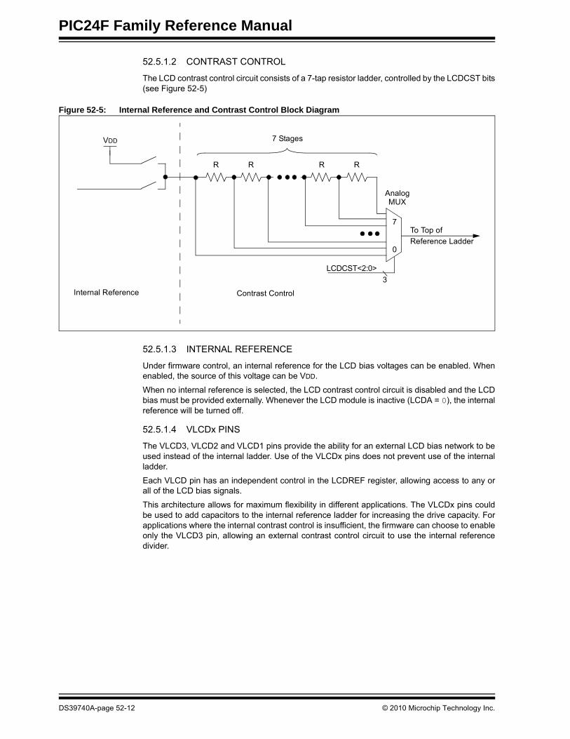
52.5.1.2 CONTRAST CONTROL
The LCD contrast control circuit consists of a 7-tap resistor ladder, controlled by the LCDCST bits(see Figure 52-5)
Figure 52-5: Internal Reference and Contrast Control Block Diagram
52.5.1.3 INTERNAL REFERENCE
Under firmware control, an internal reference for the LCD bias voltages can be enabled. Whenenabled, the source of this voltage can be VDD.
When no internal reference is selected, the LCD contrast control circuit is disabled and the LCDbias must be provided externally. Whenever the LCD module is inactive (LCDA = 0), the internalreference will be turned off.
52.5.1.4 VLCDx PINS
The VLCD3, VLCD2 and VLCD1 pins provide the ability for an external LCD bias network to beused instead of the internal ladder. Use of the VLCDx pins does not prevent use of the internalladder.
Each VLCD pin has an independent control in the LCDREF register, allowing access to any orall of the LCD bias signals.
This architecture allows for maximum flexibility in different applications. The VLCDx pins couldbe used to add capacitors to the internal reference ladder for increasing the drive capacity. Forapplications where the internal contrast control is insufficient, the firmware can choose to enableonly the VLCD3 pin, allowing an external contrast control circuit to use the internal referencedivider.
LCDCST<2:0>
Analog
R R R R
7 Stages
MUX
To Top of
Reference Ladder
7
0
3
VDD
Internal Reference Contrast Control
DS39740A-page 52-12 © 2010 Microchip Technology Inc.
Section 52. Liquid Crystal Display (LCD)L
iqu
id C
rystalD
isplay (L
CD
)
52
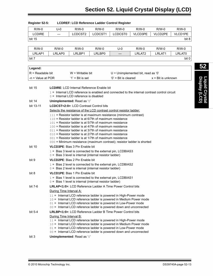
Register 52-5: LCDREF: LCD Reference Ladder Control Register
R/W-0 U-0 R/W-0 R/W-0 R/W-0 R/W-0 R/W-0 R/W-0
LCDIRE — LCDCST2 LCDCST1 LCDCST0 VLCD3PE VLCD2PE VLCD1PE
bit 15 bit 8
R/W-0 R/W-0 R/W-0 R/W-0 U-0 R/W-0 R/W-0 R/W-0
LRLAP1 LRLAP0 LRLBP1 LRLBP0 — LRLAT2 LRLAT1 LRLAT0
bit 7 bit 0
Legend:
R = Readable bit W = Writable bit U = Unimplemented bit, read as ‘0’
-n = Value at POR ‘1’ = Bit is set ‘0’ = Bit is cleared x = Bit is unknown
bit 15 LCDIRE: LCD Internal Reference Enable bit
1 = Internal LCD reference is enabled and connected to the internal contrast control circuit0 = Internal LCD reference is disabled
bit 14 Unimplemented: Read as ‘0’
bit 13-11 LCDCST<2:0>: LCD Contrast Control bits
Selects the resistance of the LCD contrast control resistor ladder:
111 = Resistor ladder is at maximum resistance (minimum contrast)110 = Resistor ladder is at 6/7th of maximum resistance101 = Resistor ladder is at 5/7th of maximum resistance100 = Resistor ladder is at 4/7th of maximum resistance011 = Resistor ladder is at 3/7th of maximum resistance010 = Resistor ladder is at 2/7th of maximum resistance001 = Resistor ladder is at 1/7th of maximum resistance000 = Minimum resistance (maximum contrast); resistor ladder is shorted
bit 10 VLCD3PE: Bias 3 Pin Enable bit
1 = Bias 3 level is connected to the external pin, LCDBIAS30 = Bias 3 level is internal (internal resistor ladder)
bit 9 VLCD2PE: Bias 2 Pin Enable bit
1 = Bias 2 level is connected to the external pin, LCDBIAS20 = Bias 2 level is internal (internal resistor ladder)
bit 8 VLCD1PE: Bias 1 Pin Enable bit
1 = Bias 1 level is connected to the external pin, LCDBIAS10 = Bias 1 level is internal (internal resistor ladder)
bit 7-6 LRLAP<1:0>: LCD Reference Ladder A Time Power Control bits
During Time Interval A:
11 = Internal LCD reference ladder is powered in High-Power mode10 = Internal LCD reference ladder is powered in Medium Power mode01 = Internal LCD reference ladder is powered in Low-Power mode00 = Internal LCD reference ladder is powered down and unconnected
bit 5-4 LRLBP<1:0>: LCD Reference Ladder B Time Power Control bits
During Time Interval B:11 = Internal LCD reference ladder is powered in High-Power mode10 = Internal LCD reference ladder is powered in Medium Power mode01 = Internal LCD reference ladder is powered in Low-Power mode00 = Internal LCD reference ladder is powered down and unconnected
bit 3 Unimplemented: Read as ‘0’
© 2010 Microchip Technology Inc. DS39740A-page 52-13
PIC24F Family Reference Manual
52.5.2 LCD Bias Generation
The LCD driver module is capable of generating the required bias voltages for LCD operationwith a minimum of external components. This includes the ability to generate the different voltagelevels required by the different bias types that are required by the LCD. The driver module canalso provide bias voltages, both above and below microcontroller VDD, through the use of anon-chip LCD voltage regulator.
52.5.2.1 LCD BIAS TYPES
PIC24FJXXXGA3XX family devices support three bias types based on the waveforms generatedto control segments and commons:
• Static (two discrete levels)
• 1/2 Bias (three discrete levels
• 1/3 Bias (four discrete levels)
The use of different waveforms in driving the LCD is discussed in more detail in Section 52.10“LCD Waveform Generation”.
52.5.2.2 LCD VOLTAGE REGULATOR
The purpose of the LCD regulator is to provide proper bias voltage and good contrast for theLCD, regardless of VDD levels. This module contains a charge pump and internal voltage refer-ence. The regulator can be configured by using external components to boost bias voltage aboveVDD. It can also operate a display at a constant voltage below VDD. The regulator can also beselectively disabled to allow bias voltages to be generated by an external resistor network.
The LCD regulator is controlled through the LCDREG register (Register 52-6). It is enabled ordisabled using the CKSEL<1:0> bits, while the charge pump can be selectively enabled usingthe CPEN bit. When the regulator is enabled, the MODE13 bit is used to select the bias type. Thepeak LCD bias voltage, measured as a difference between the potentials of LCDBIAS3 andLCDBIAS0, is configured with the BIAS bits.
bit 2-0 LRLAT<2:0>: LCD Reference Ladder A Time Interval Control bits
Sets the number of 32 clock counts when the A Time Interval Power mode is active.
For Type-A Waveforms (WFT = 0):111 = Internal LCD reference ladder is in A Power mode for 7 clocks and B Power mode for 9 clocks110 = Internal LCD reference ladder is in A Power mode for 6 clocks and B Power mode for 10 clocks101 = Internal LCD reference ladder is in A Power mode for 5 clocks and B Power mode for 11 clocks100 = Internal LCD reference ladder is in A Power mode for 4 clocks and B Power mode for 12 clocks011 = Internal LCD reference ladder is in A Power mode for 3 clocks and B Power mode for 13 clocks010 = Internal LCD reference ladder is in A Power mode for 2 clocks and B Power mode for 14 clocks001 = Internal LCD reference ladder is in A Power mode for 1 clock and B Power mode for 15 clocks000 = Internal LCD reference ladder is always in B Power mode
For Type-B Waveforms (WFT = 1):111 = Internal LCD reference ladder is in A Power mode for 7 clocks and B Power mode for 25 clocks110 = Internal LCD reference ladder is in A Power mode for 6 clocks and B Power mode for 26 clocks101 = Internal LCD reference ladder is in A Power mode for 5 clocks and B Power mode for 27 clocks100 = Internal LCD reference ladder is in A Power mode for 4 clocks and B Power mode for 28 clocks011 = Internal LCD reference ladder is in A Power mode for 3 clocks and B Power mode for 29 clocks010 = Internal LCD reference ladder is in A Power mode for 2 clocks and B Power mode for 30 clocks001 = Internal LCD reference ladder is in A Power mode for 1 clock and B Power mode for 31 clocks000 = Internal LCD reference ladder is always in B Power mode
DS39740A-page 52-14 © 2010 Microchip Technology Inc.
Section 52. Liquid Crystal Display (LCD)L
iqu
id C
rystalD
isplay (L
CD
)
52
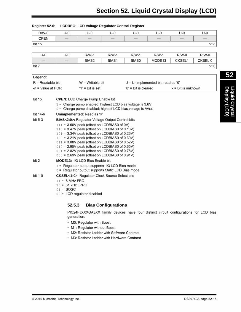
Register 52-6: LCDREG: LCD Voltage Regulator Control Register
52.5.3 Bias Configurations
PIC24FJXXXGA3XX family devices have four distinct circuit configurations for LCD biasgeneration:
• M0: Regulator with Boost
• M1: Regulator without Boost
• M2: Resistor Ladder with Software Contrast
• M3: Resistor Ladder with Hardware Contrast
R/W-0 U-0 U-0 U-0 U-0 U-0 U-0 U-0
CPEN — — — — — — —
bit 15 bit 8
U-0 U-0 R/W-1 R/W-1 R/W-1 R/W-1 R/W-0 R/W-0
— — BIAS2 BIAS1 BIAS0 MODE13 CKSEL1 CKSEL 0
bit 7 bit 0
Legend:
R = Readable bit W = Writable bit U = Unimplemented bit, read as ‘0’
-n = Value at POR ‘1’ = Bit is set ‘0’ = Bit is cleared x = Bit is unknown
bit 15 CPEN: LCD Charge Pump Enable bit
1 = Charge pump enabled; highest LCD bias voltage is 3.6V0 = Charge pump disabled; highest LCD bias voltage is AVDD
bit 14-6 Unimplemented: Read as ‘0’
bit 5-3 BIAS<2:0>: Regulator Voltage Output Control bits
111 = 3.60V peak (offset on LCDBIAS0 of 0V)110 = 3.47V peak (offset on LCDBIAS0 of 0.13V)101 = 3.34V peak (offset on LCDBIAS0 of 0.26V)100 = 3.21V peak (offset on LCDBIAS0 of 0.39V)011 = 3.08V peak (offset on LCDBIAS0 of 0.52V)010 = 2.95V peak (offset on LCDBIAS0 of 0.65V)001 = 2.82V peak (offset on LCDBIAS0 of 0.78V)000 = 2.69V peak (offset on LCDBIAS0 of 0.91V)
bit 2 MODE13: 1/3 LCD Bias Enable bit
1 = Regulator output supports 1/3 LCD Bias mode0 = Regulator output supports Static LCD Bias mode
bit 1-0 CKSEL<1:0>: Regulator Clock Source Select bits
11 = 8 MHz FRC10 = 31 kHz LPRC01 = SOSC00 = LCD regulator disabled
© 2010 Microchip Technology Inc. DS39740A-page 52-15
PIC24F Family Reference Manual
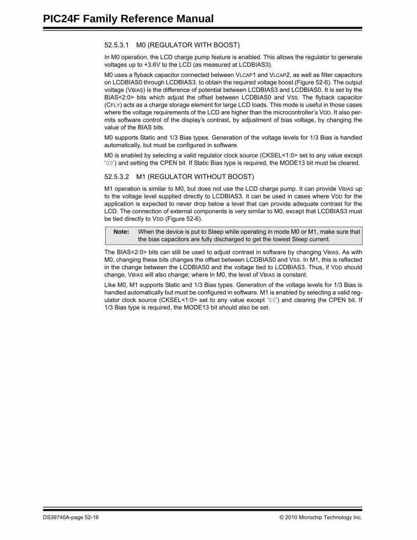
52.5.3.1 M0 (REGULATOR WITH BOOST)
In M0 operation, the LCD charge pump feature is enabled. This allows the regulator to generatevoltages up to +3.6V to the LCD (as measured at LCDBIAS3).
M0 uses a flyback capacitor connected between VLCAP1 and VLCAP2, as well as filter capacitorson LCDBIAS0 through LCDBIAS3, to obtain the required voltage boost (Figure 52-6). The outputvoltage (VBIAS) is the difference of potential between LCDBIAS3 and LCDBIAS0. It is set by theBIAS<2:0> bits which adjust the offset between LCDBIAS0 and VSS. The flyback capacitor(CFLY) acts as a charge storage element for large LCD loads. This mode is useful in those caseswhere the voltage requirements of the LCD are higher than the microcontroller’s VDD. It also per-mits software control of the display’s contrast, by adjustment of bias voltage, by changing thevalue of the BIAS bits.
M0 supports Static and 1/3 Bias types. Generation of the voltage levels for 1/3 Bias is handledautomatically, but must be configured in software.
M0 is enabled by selecting a valid regulator clock source (CKSEL<1:0> set to any value except‘00’) and setting the CPEN bit. If Static Bias type is required, the MODE13 bit must be cleared.
52.5.3.2 M1 (REGULATOR WITHOUT BOOST)
M1 operation is similar to M0, but does not use the LCD charge pump. It can provide VBIAS upto the voltage level supplied directly to LCDBIAS3. It can be used in cases where VDD for theapplication is expected to never drop below a level that can provide adequate contrast for theLCD. The connection of external components is very similar to M0, except that LCDBIAS3 mustbe tied directly to VDD (Figure 52-6).
The BIAS<2:0> bits can still be used to adjust contrast in software by changing VBIAS. As withM0, changing these bits changes the offset between LCDBIAS0 and VSS. In M1, this is reflectedin the change between the LCDBIAS0 and the voltage tied to LCDBIAS3. Thus, if VDD shouldchange, VBIAS will also change; where in M0, the level of VBIAS is constant.
Like M0, M1 supports Static and 1/3 Bias types. Generation of the voltage levels for 1/3 Bias ishandled automatically but must be configured in software. M1 is enabled by selecting a valid reg-ulator clock source (CKSEL<1:0> set to any value except ‘00’) and clearing the CPEN bit. If1/3 Bias type is required, the MODE13 bit should also be set.
Note: When the device is put to Sleep while operating in mode M0 or M1, make sure thatthe bias capacitors are fully discharged to get the lowest Sleep current.
DS39740A-page 52-16 © 2010 Microchip Technology Inc.
Section 52. Liquid Crystal Display (LCD)L
iqu
id C
rystalD
isplay (L
CD
)
52
Figure 52-6: LCD Regulator Connections for M0 and M1 Configurations
LCDBIAS3
LCDBIAS2
LCDBIAS1
LCDBIAS0
AVDD
VDD
VLCAP1
VLCAP2
CFLY
C0
C1
C2
C3
C0
C1
C2
VDD
VDD
Mode 0 (VBIAS up to 3.6V) Mode 1 (VBIAS VDD)
CFLY
Note 1: These values are provided for design guidance only. They should be optimized for the application by the designer based on the actual LCD specifications.
0.47 F(1)
0.47 F(1)
0.47 F(1)
0.47 F(1)
0.47 F(1)
0.47 F(1)
0.47 F(1)
0.47 F(1)
0.47 F(1)
PIC24FJXXXGA3XX
© 2010 Microchip Technology Inc. DS39740A-page 52-17
PIC24F Family Reference Manual
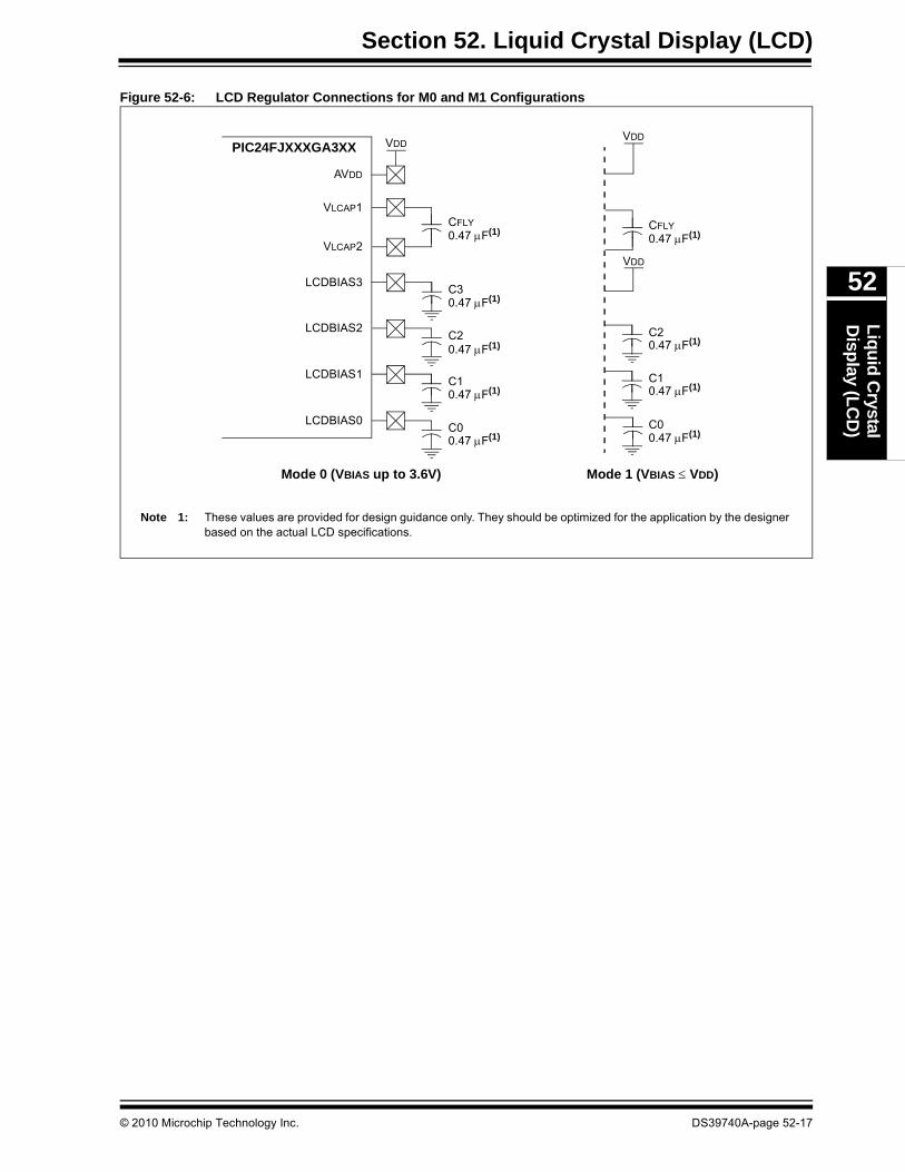
52.5.3.3 M2 (EXTERNAL RESISTOR LADDER WITH SOFTWARE CONTRAST)
M2 operation also uses the LCD regulator but disables the charge pump. The regulator’s internalvoltage reference remains active as a way to regulate contrast. It is used in cases where thecurrent requirements of the LCD exceed the capacity of the regulator’s charge pump.
In this configuration, the LCD bias voltage levels are created by an external resistor voltagedivider, connected across LCDBIAS0 through LCDBIAS3, with the top of the divider tied to VDD
(Figure 52-7). The potential at the bottom of the ladder is determined by the LCD regulator’s volt-age reference, tied internally to LCDBIAS0. The bias type is determined by the voltages on theLCDBIAS pins, which are controlled by the configuration of the resistor ladder. Most applicationsusing M2 will use a 1/3 or 1/2 Bias type. While Static Bias can also be used, it offers extremelylimited contrast range and additional current consumption over other bias generation modes.
Like M1, the LCDBIAS bits can be used to control contrast, limited by the level of VDD suppliedto the device. Also, since there is no capacitor required across VLCAP1 and VLCAP2, these pinsare available as digital I/O ports, RG2 and RG3. M2 is selected by clearing the CKSEL<1:0> bitsand setting the CPEN bit.
Figure 52-7: Resistor Ladder Connections for M2 Configuration
LCDBIAS3
Note 1: These values are provided for design guidance only. They should be optimized for the application by the designerbased on the actual LCD specifications.
Bias Level at PinBias Type
1/2 Bias 1/3 Bias
LCDBIAS0 (Internal Low Reference Voltage) (Internal Low Reference Voltage)
LCDBIAS1 1/2 VBIAS 1/3 VBIAS
LCDBIAS2 1/2 VBIAS 2/3 VBIAS
LCDBIAS3 VBIAS (up to AVDD) VBIAS (up to AVDD)
10 k(1)
10 k(1)
1/2 Bias 1/3 Bias
LCDBIAS2
LCDBIAS1
LCDBIAS0
AVDD
10 k(1)
10 k(1)
10 k(1)
VDD
PIC24FJXXXGA3XX
DS39740A-page 52-18 © 2010 Microchip Technology Inc.
Section 52. Liquid Crystal Display (LCD)L
iqu
id C
rystalD
isplay (L
CD
)
52
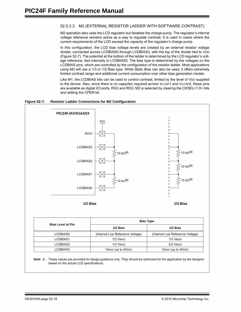
52.5.3.4 M3 (HARDWARE CONTRAST)
In M3, the LCD regulator is completely disabled. Like M2, LCD bias levels are tied to AVDD andare generated using an external divider. The difference is that the internal voltage reference isalso disabled and the bottom of the ladder is tied to ground (VSS); see Figure 52-8. The value ofthe resistors, and the difference between VSS and VDD, determine the contrast range; no soft-ware adjustment is possible. This configuration is also used where the LCD module’s currentrequirements exceed the capacity of the charge pump and software contrast control is notneeded.
Depending on the bias type required, resistors are connected between some or all of the pins. Apotentiometer can also be connected between LCDBIAS3 and VDD to allow for hardwarecontrolled contrast adjustment.
M3 is selected by clearing the CKSEL<1:0> and CPEN bits.
Figure 52-8: Resistor Ladder Connections for M3 Configuration
LCDBIAS3
Note 1: These values are provided for design guidance only. They should be optimized for the application by thedesigner based on the actual LCD specifications.
2: A potentiometer for manual contrast adjustment is optional; it may be omitted entirely.
Bias Level at PinBias Type
Static 1/2 Bias 1/3 Bias
LCDBIAS0 AVSS AVSS AVSS
LCDBIAS1 AVSS 1/2 AVDD 1/3 AVDD
LCDBIAS2 AVDD 1/2 AVDD 2/3 AVDD
LCDBIAS3 AVDD AVDD AVDD
10 k(1)
10 k(1)
Static Bias 1/2 Bias 1/3 Bias
LCDBIAS2
LCDBIAS1
LCDBIAS0
AVDD
10 k(1)
10 k(1)
10 k(1)
VDD
(2)
PIC24FJXXXGA3XX
© 2010 Microchip Technology Inc. DS39740A-page 52-19
PIC24F Family Reference Manual
52.5.4 Design Considerations For The LCD Charge Pump
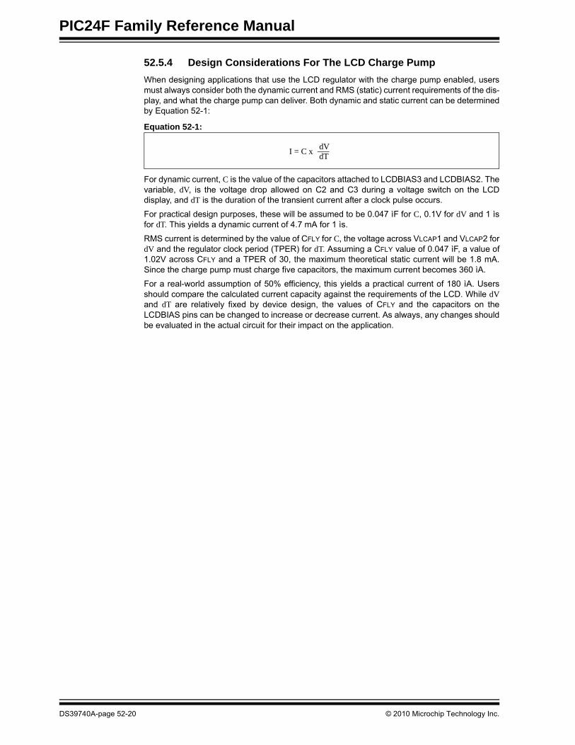
When designing applications that use the LCD regulator with the charge pump enabled, usersmust always consider both the dynamic current and RMS (static) current requirements of the dis-play, and what the charge pump can deliver. Both dynamic and static current can be determinedby Equation 52-1:
Equation 52-1:
For dynamic current, C is the value of the capacitors attached to LCDBIAS3 and LCDBIAS2. Thevariable, dV, is the voltage drop allowed on C2 and C3 during a voltage switch on the LCDdisplay, and dT is the duration of the transient current after a clock pulse occurs.
For practical design purposes, these will be assumed to be 0.047 ìF for C, 0.1V for dV and 1 ìsfor dT. This yields a dynamic current of 4.7 mA for 1 ìs.
RMS current is determined by the value of CFLY for C, the voltage across VLCAP1 and VLCAP2 fordV and the regulator clock period (TPER) for dT. Assuming a CFLY value of 0.047 ìF, a value of1.02V across CFLY and a TPER of 30, the maximum theoretical static current will be 1.8 mA.Since the charge pump must charge five capacitors, the maximum current becomes 360 ìA.
For a real-world assumption of 50% efficiency, this yields a practical current of 180 ìA. Usersshould compare the calculated current capacity against the requirements of the LCD. While dVand dT are relatively fixed by device design, the values of CFLY and the capacitors on theLCDBIAS pins can be changed to increase or decrease current. As always, any changes shouldbe evaluated in the actual circuit for their impact on the application.
I = C xdVdT
DS39740A-page 52-20 © 2010 Microchip Technology Inc.
Section 52. Liquid Crystal Display (LCD)L
iqu
id C
rystalD
isplay (L
CD
)
52
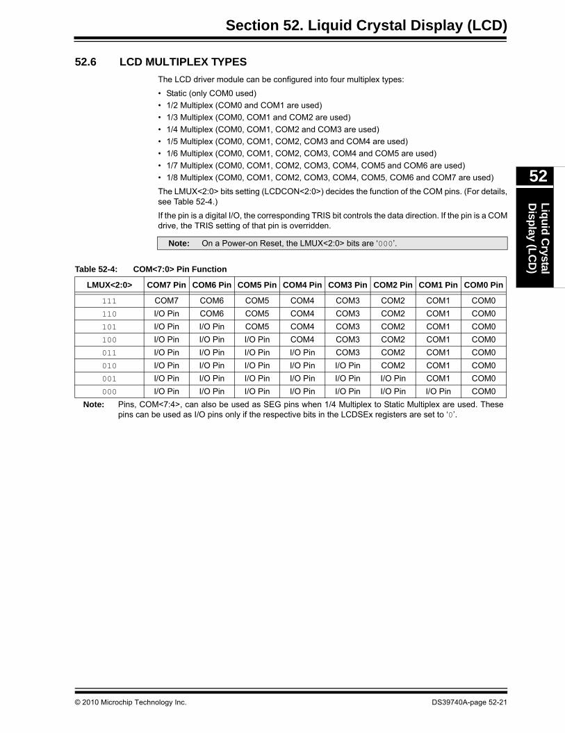
52.6 LCD MULTIPLEX TYPES
The LCD driver module can be configured into four multiplex types:
• Static (only COM0 used)
• 1/2 Multiplex (COM0 and COM1 are used)
• 1/3 Multiplex (COM0, COM1 and COM2 are used)
• 1/4 Multiplex (COM0, COM1, COM2 and COM3 are used)
• 1/5 Multiplex (COM0, COM1, COM2, COM3 and COM4 are used)
• 1/6 Multiplex (COM0, COM1, COM2, COM3, COM4 and COM5 are used)
• 1/7 Multiplex (COM0, COM1, COM2, COM3, COM4, COM5 and COM6 are used)
• 1/8 Multiplex (COM0, COM1, COM2, COM3, COM4, COM5, COM6 and COM7 are used)
The LMUX<2:0> bits setting (LCDCON<2:0>) decides the function of the COM pins. (For details,see Table 52-4.)
If the pin is a digital I/O, the corresponding TRIS bit controls the data direction. If the pin is a COMdrive, the TRIS setting of that pin is overridden.
Note: On a Power-on Reset, the LMUX<2:0> bits are ‘000’.
Table 52-4: COM<7:0> Pin Function
LMUX<2:0> COM7 Pin COM6 Pin COM5 Pin COM4 Pin COM3 Pin COM2 Pin COM1 Pin COM0 Pin
111 COM7 COM6 COM5 COM4 COM3 COM2 COM1 COM0
110 I/O Pin COM6 COM5 COM4 COM3 COM2 COM1 COM0
101 I/O Pin I/O Pin COM5 COM4 COM3 COM2 COM1 COM0
100 I/O Pin I/O Pin I/O Pin COM4 COM3 COM2 COM1 COM0
011 I/O Pin I/O Pin I/O Pin I/O Pin COM3 COM2 COM1 COM0
010 I/O Pin I/O Pin I/O Pin I/O Pin I/O Pin COM2 COM1 COM0
001 I/O Pin I/O Pin I/O Pin I/O Pin I/O Pin I/O Pin COM1 COM0
000 I/O Pin I/O Pin I/O Pin I/O Pin I/O Pin I/O Pin I/O Pin COM0
Note: Pins, COM<7:4>, can also be used as SEG pins when 1/4 Multiplex to Static Multiplex are used. Thesepins can be used as I/O pins only if the respective bits in the LCDSEx registers are set to ‘0’.
© 2010 Microchip Technology Inc. DS39740A-page 52-21
PIC24F Family Reference Manual
52.7 SEGMENT ENABLES
The LCDSEx registers are used to select the pin function for each segment pin. The selectionallows each pin to operate as either an LCD segment driver or a digital only pin. To configure thepin as a segment pin, the corresponding bits in the LCDSEx registers must be set to ‘1’.
If the pin is a digital I/O, the corresponding TRIS bit controls the data direction. Any bit set in theLCDSEx registers overrides any bit settings in the corresponding TRIS register.
52.8 PIXEL CONTROL
The LCDDATAx registers contain bits that define the state of each pixel. Each bit defines oneunique pixel. Table 52-2 shows the correlation of each bit in the LCDDATAx registers to therespective common and segment signals.
Any LCD pixel location not being used for display can be used as general purpose RAM.
52.9 LCD FRAME FREQUENCY
The rate at which the COM and SEG outputs change is called the LCD frame frequency.
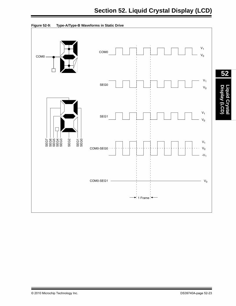
52.10 LCD WAVEFORM GENERATION
LCD waveform generation is based on the philosophy that the net AC voltage across the darkpixel should be maximized and the net AC voltage across the clear pixel should be minimized.The net DC voltage across any pixel should be zero.
The COM signal represents the time slice for each common, while the SEG contains the pixel data.
The pixel signal (COM-SEG) will have no DC component and can take only one of the two rmsvalues. The higher rms value will create a dark pixel and a lower rms value will create a clearpixel.
As the number of commons increases, the delta between the two rms values decreases. Thedelta represents the maximum contrast that the display can have.
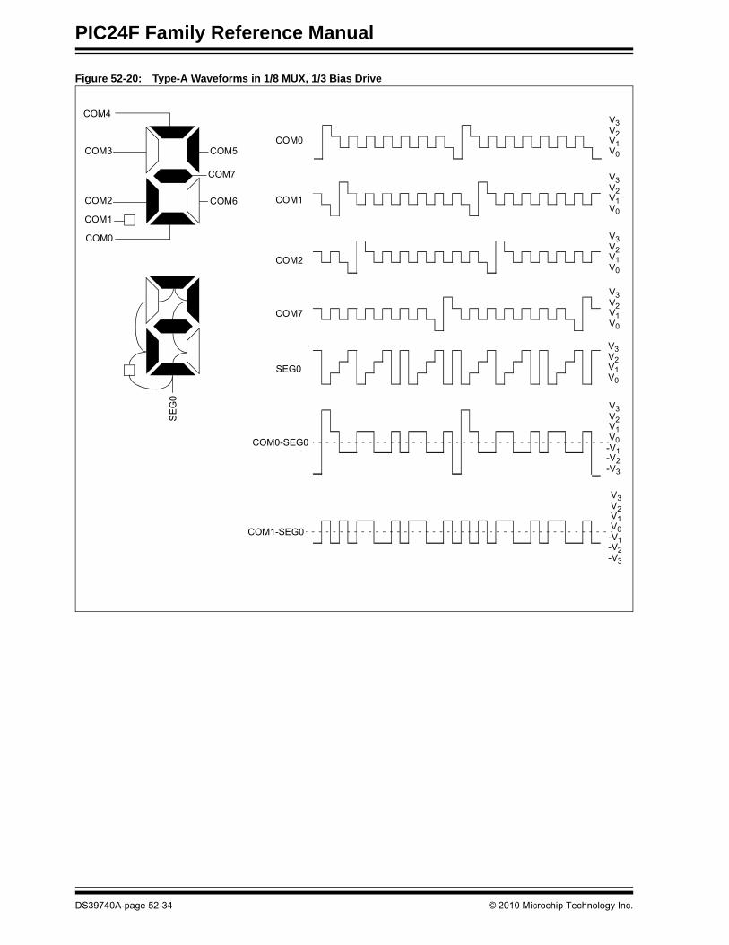
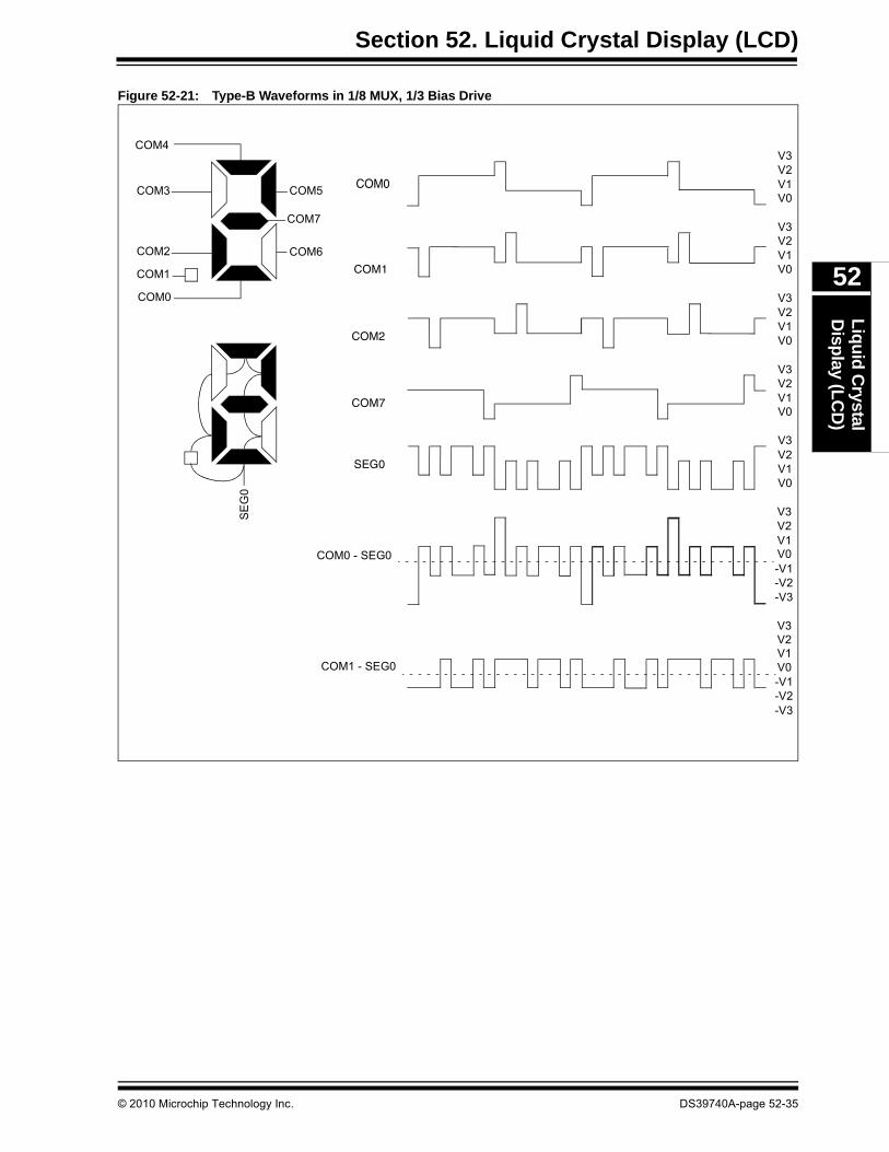
The LCDs can be driven by two types of waveforms: Type-A and Type-B. In a Type-A waveform,the phase changes within each common type, whereas a Type-B waveform’s phase changes oneach frame boundary. Thus, Type-A waveforms maintain 0 VDC over a single frame, whereasType-B waveforms take two frames.
Figure 52-9 through Figure 52-21 provide waveforms for Static, Half-Multiplex, One-ThirdMultiplex and Quarter Multiplex drives for Type-A and Type-B waveforms.
Note: On a Power-on Reset, these pins are configured as digital I/O.
Table 52-5: Frame Frequency Formulas
Multiplex Frame Frequency =
Static (000) Clock Source/(4 x 1 x (LP<3:0> + 1))
1/2 (001) Clock Source/(2 x 2 x (LP<3:0> + 1))
1/3 (010) Clock Source/(1 x 3 x (LP<3:0> + 1))
1/4 (011) Clock Source/(1 x 4 x (LP<3:0> + 1))
1/5 (100) Clock Source/(1 x 5 x (LP<3:0> + 1))
1/6 (101) Clock Source/(1 x 6 x (LP<3:0> + 1))
1/7 (110) Clock Source/(1 x 7 x (LP<3:0> + 1))
1/8 (111) Clock Source/(1 x 8 x (LP<3:0> + 1))
Note: Clock source is FRC/8192, SOSC/32 or LPRC/32.
Note: If Sleep has to be executed with LCD Sleep enabled (SLPEN (LCDCON<6>) = 1),care must be taken to execute Sleep only when the VDC on all the pixels is ‘0’.
DS39740A-page 52-22 © 2010 Microchip Technology Inc.
Section 52. Liquid Crystal Display (LCD)L
iqu
id C
rystalD
isplay (L
CD
)
52
Figure 52-9: Type-A/Type-B Waveforms in Static Drive
V1
V0
COM0
SEG0
COM0-SEG0
COM0-SEG1
SEG1
V1
V0
V1
V0
V0
V1
-V1
V0
1 Frame
COM0
SE
G0
SE
G1
SE
G2
SE
G3
SE
G4
SE
G5
SE
G6
SE
G7
© 2010 Microchip Technology Inc. DS39740A-page 52-23
PIC24F Family Reference Manual
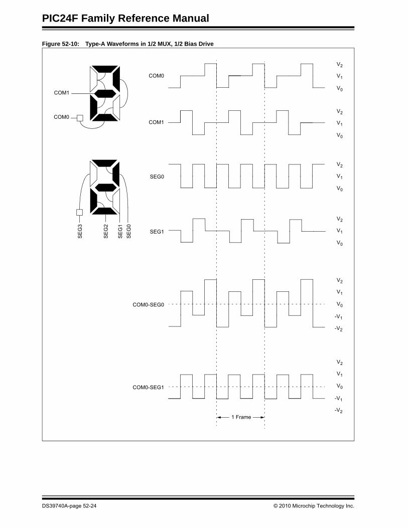
Figure 52-10: Type-A Waveforms in 1/2 MUX, 1/2 Bias Drive
V2
V1
V0
V2
V1
V0
V2
V1
V0
V2
V1
V0
V2
V1
V0
-V2
-V1
V2
V1
V0
-V2
-V1
COM0
COM1
SEG0
SEG1
COM0-SEG0
COM0-SEG1
1 Frame
COM1
COM0
SE
G0
SE
G1
SE
G2
SE
G3
DS39740A-page 52-24 © 2010 Microchip Technology Inc.
Section 52. Liquid Crystal Display (LCD)L
iqu
id C
rystalD
isplay (L
CD
)
52
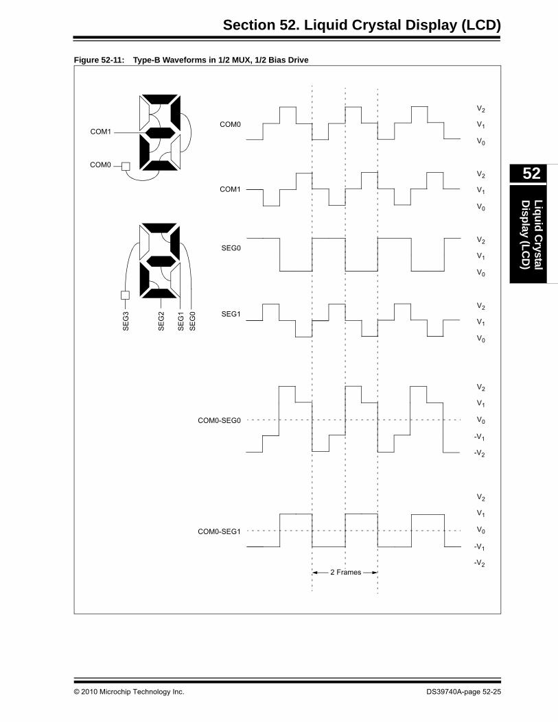
Figure 52-11: Type-B Waveforms in 1/2 MUX, 1/2 Bias Drive
V2
V1
V0
V2
V1
V0
V2
V1
V0
V2
V1
V0
V2
V1
V0
-V2
-V1
V2
V1
V0
-V2
-V1
COM0
COM1
SEG0
SEG1
COM0-SEG0
COM0-SEG1
COM1
COM0
SE
G0
SE
G1
SE
G2
SE
G3
2 Frames
© 2010 Microchip Technology Inc. DS39740A-page 52-25
PIC24F Family Reference Manual
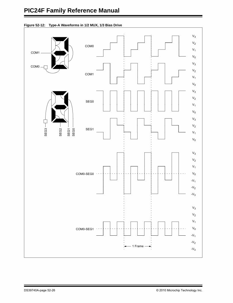
Figure 52-12: Type-A Waveforms in 1/2 MUX, 1/3 Bias Drive
V3
V2
V1
V0
V3
V2
V1
V0
V3
V2
V1
V0
V3
V2
V1
V0
V3
V2
V1
V0
-V3
-V2
-V1
V3
V2
V1
V0
-V3
-V2
-V1
COM0
COM1
SEG0
SEG1
COM0-SEG0
COM0-SEG1
1 Frame
COM1
COM0
SE
G0
SE
G1
SE
G2
SE
G3
DS39740A-page 52-26 © 2010 Microchip Technology Inc.
Section 52. Liquid Crystal Display (LCD)L
iqu
id C
rystalD
isplay (L
CD
)
52
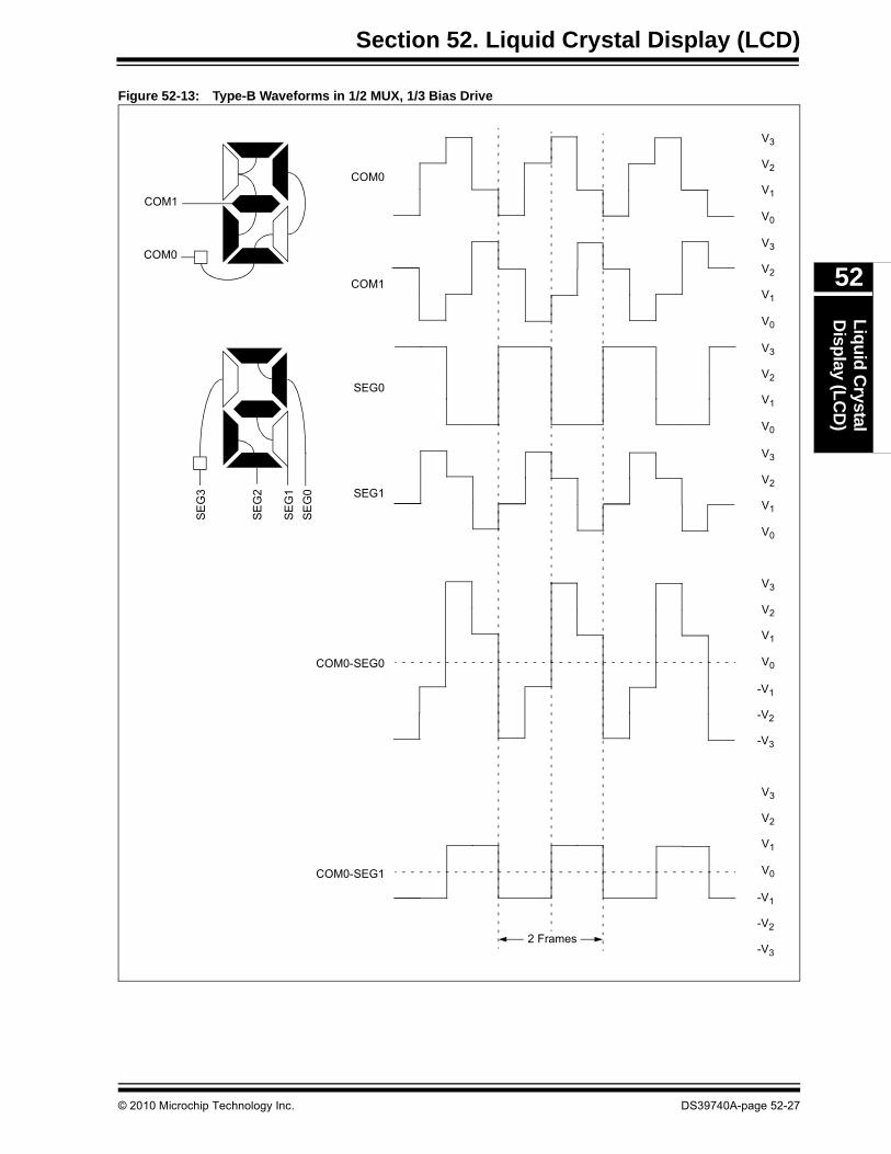
Figure 52-13: Type-B Waveforms in 1/2 MUX, 1/3 Bias Drive
V3
V2
V1
V0
V3
V2
V1
V0
V3
V2
V1
V0
V3
V2
V1
V0
V3
V2
V1
V0
-V3
-V2
-V1
V3
V2
V1
V0
-V3
-V2
-V1
COM0
COM1
SEG0
SEG1
COM0-SEG0
COM0-SEG1
COM1
COM0
SE
G0
SE
G1
SE
G2
SE
G3
2 Frames
© 2010 Microchip Technology Inc. DS39740A-page 52-27
PIC24F Family Reference Manual
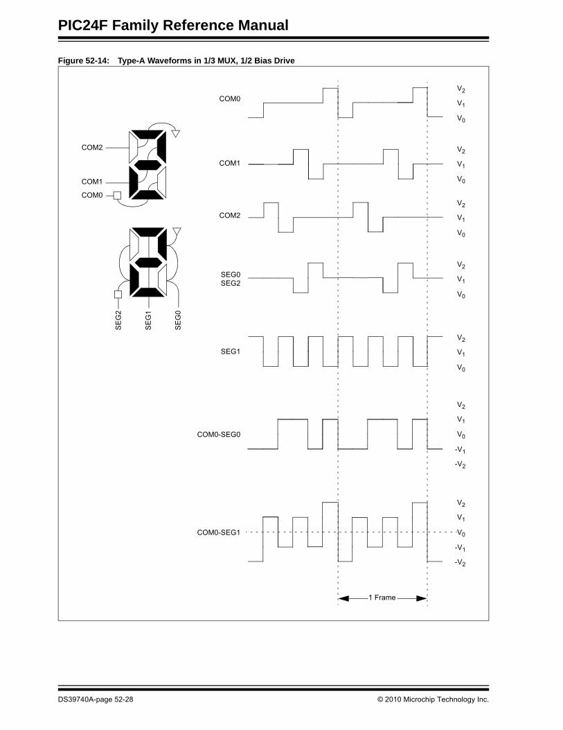
Figure 52-14: Type-A Waveforms in 1/3 MUX, 1/2 Bias Drive
V2
V1
V0
V2
V1
V0
V2
V1
V0
V2
V1
V0
V2
V1
V0
V2
V1
V0
-V2
-V1
V2
V1
V0
-V2
-V1
COM0
COM1
COM2
SEG0
SEG1
COM0-SEG0
COM0-SEG1
1 Frame
COM2
COM1
COM0
SE
G0
SE
G1
SE
G2
SEG2
DS39740A-page 52-28 © 2010 Microchip Technology Inc.
Section 52. Liquid Crystal Display (LCD)L
iqu
id C
rystalD
isplay (L
CD
)
52
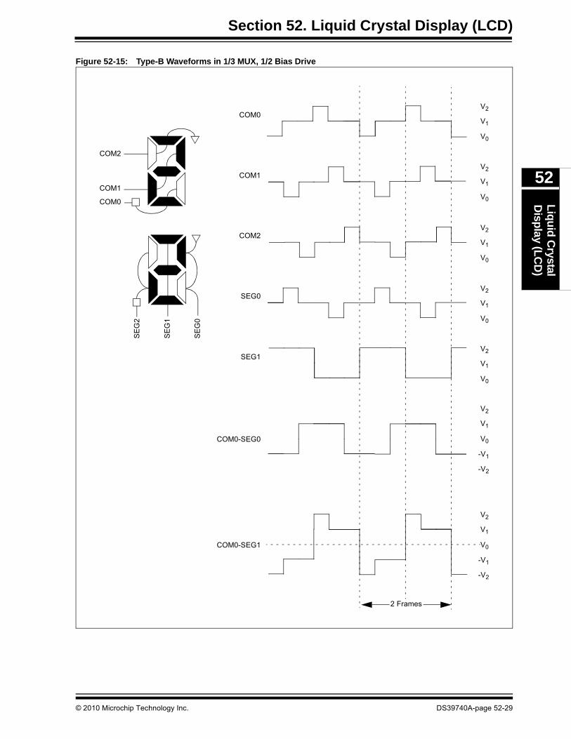
Figure 52-15: Type-B Waveforms in 1/3 MUX, 1/2 Bias Drive
V2
V1
V0
V2
V1
V0
V2
V1
V0
V2
V1
V0
V2
V1
V0
V2
V1
V0
-V2
-V1
V2
V1
V0
-V2
-V1
COM0
COM1
COM2
SEG0
SEG1
COM0-SEG0
COM0-SEG1
2 Frames
COM2
COM1
COM0S
EG
0
SE
G1
SE
G2
© 2010 Microchip Technology Inc. DS39740A-page 52-29
PIC24F Family Reference Manual
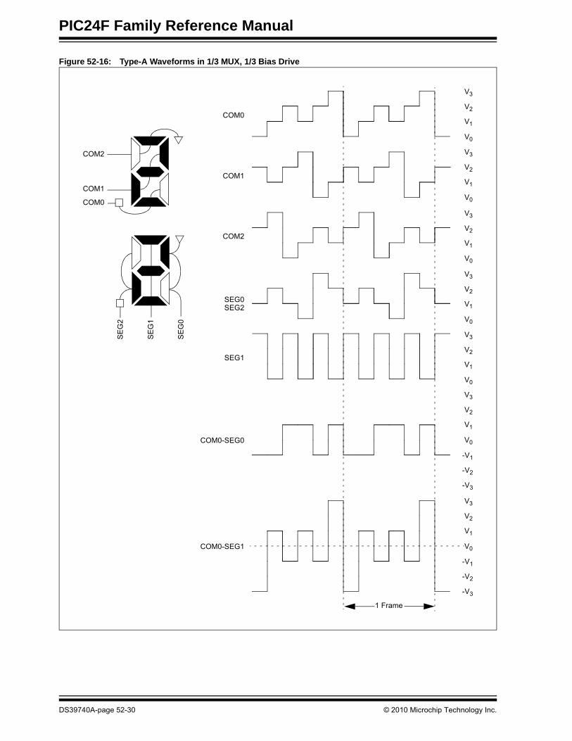
Figure 52-16: Type-A Waveforms in 1/3 MUX, 1/3 Bias Drive
V3
V2
V1
V0
V3
V2
V1
V0
V3
V2
V1
V0
V3
V2
V1
V0
V3
V2
V1
V0
V3
V2
V1
V0
-V3
-V2
-V1
V3
V2
V1
V0
-V3
-V2
-V1
COM0
COM1
COM2
SEG0
SEG1
COM0-SEG0
COM0-SEG1
1 Frame
COM2
COM1
COM0
SE
G0
SE
G1
SE
G2
SEG2
DS39740A-page 52-30 © 2010 Microchip Technology Inc.

Section 52. Liquid Crystal Display (LCD)L
iqu
id C
rystalD
isplay (L
CD
)
52
Figure 52-17: Type-B Waveforms in 1/3 MUX, 1/3 Bias Drive
V3
V2
V1
V0
V3
V2
V1
V0
V3
V2
V1
V0
V3
V2
V1
V0
V3
V2
V1
V0
V3
V2
V1
V0
-V3
-V2
-V1
V3
V2
V1
V0
-V3
-V2
-V1
COM0
COM1
COM2
SEG0
SEG1
COM0-SEG0
COM0-SEG1
2 Frames
COM2
COM1
COM0S
EG
0
SE
G1
SE
G2
© 2010 Microchip Technology Inc. DS39740A-page 52-31
PIC24F Family Reference Manual
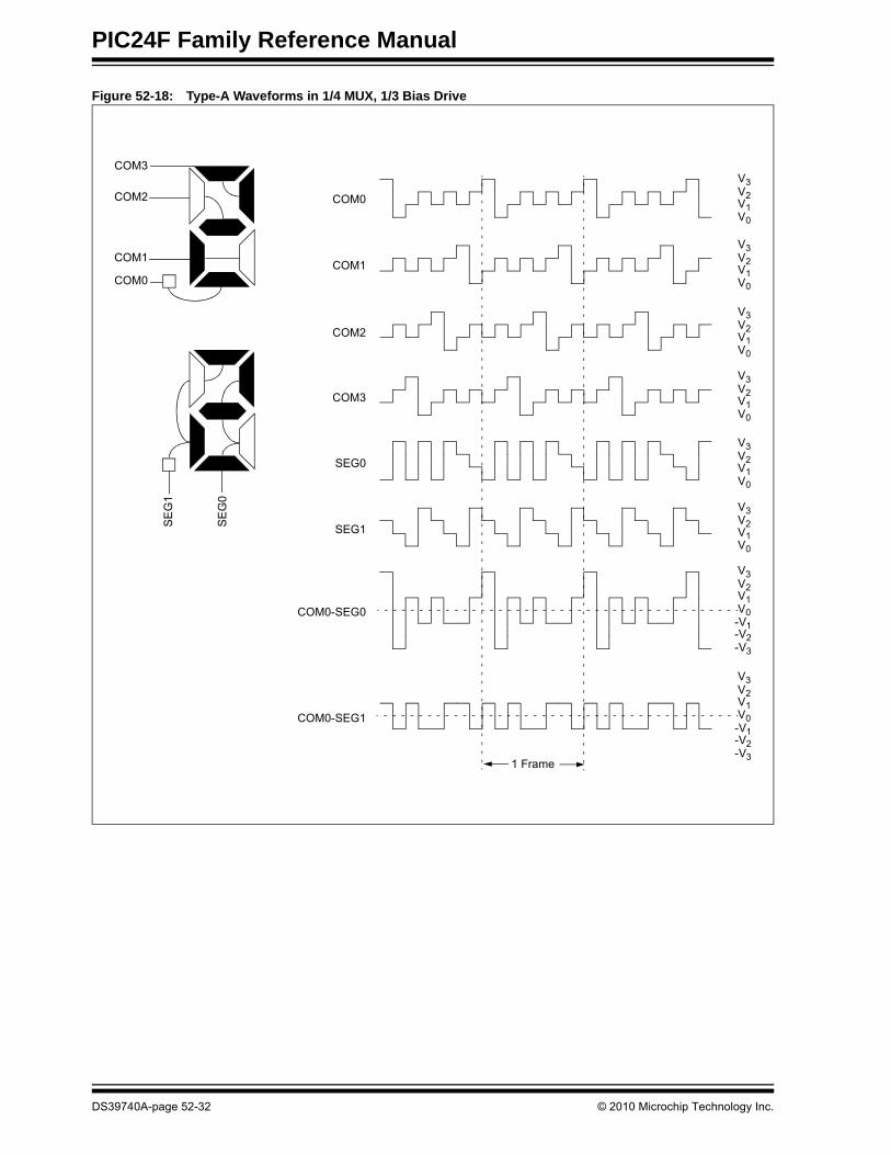
Figure 52-18: Type-A Waveforms in 1/4 MUX, 1/3 Bias Drive
V3V2V1V0
V3V2V1V0
V3V2V1V0
V3V2V1V0
V3V2V1V0
V3V2V1V0
V3V2V1V0
-V3
-V2
-V1
V3V2V1V0
-V3
-V2
-V1
COM0
COM1
COM2
COM3
SEG0
SEG1
COM0-SEG0
COM0-SEG1
COM3
COM2
COM1
COM0
1 Frame
SE
G0
SE
G1
DS39740A-page 52-32 © 2010 Microchip Technology Inc.

Section 52. Liquid Crystal Display (LCD)L
iqu
id C
rystalD
isplay (L
CD
)
52
Figure 52-19: Type-B Waveforms in 1/4 MUX, 1/3 Bias Drive
V3V2V1V0
V3V2V1V0
V3V2V1V0
V3V2V1V0
V3V2V1V0
V3V2V1V0
V3V2V1V0
-V3
-V2
-V1
V3V2V1V0
-V3
-V2
-V1
COM0
COM1
COM2
COM3
SEG0
SEG1
COM0-SEG0
COM0-SEG1
COM3
COM2
COM1
COM0
2 Frames
SE
G0
SE
G1
© 2010 Microchip Technology Inc. DS39740A-page 52-33
PIC24F Family Reference Manual
Figure 52-20: Type-A Waveforms in 1/8 MUX, 1/3 Bias Drive
COM4
COM3
COM2
COM1
SE
G0
COM5
COM7
COM6
COM0
COM0
COM1
COM2
COM7
SEG0
COM0-SEG0
COM1-SEG0
V3V2V1V0
V3V2V1V0
V3V2V1V0
V3V2V1V0
V3V2V1V0
-V3
-V2
-V1
V3V2V1V0
-V3
-V2
-V1
V3V2V1V0
DS39740A-page 52-34 © 2010 Microchip Technology Inc.
Section 52. Liquid Crystal Display (LCD)L
iqu
id C
rystalD
isplay (L
CD
)
52
Figure 52-21: Type-B Waveforms in 1/8 MUX, 1/3 Bias Drive
COM4
COM3
COM2
COM1
SE
G0
COM5
COM7
COM6
COM0
V3V2
COM0 V1V0
V3V2V1
COM1 V0
V3V2V1
COM2 V0
V3V2V1COM7V0
V3V2
SEG0 V1V0
V3V2V1V0COM0 - SEG0-V1-V2-V3
V3V2V1V0COM1 - SEG0-V1-V2-V3
© 2010 Microchip Technology Inc. DS39740A-page 52-35
PIC24F Family Reference Manual
52.11 LCD INTERRUPTS
The LCD timing generation provides an interrupt that defines the LCD frame timing. This interruptcan be used to coordinate the writing of the pixel data with the start of a new frame, whichproduces a visually crisp transition of the image.
This interrupt can also be used to synchronize external events to the LCD. For example, the inter-face to an external segment driver can be synchronized for segment data updates to the LCDframe.
A new frame is defined as beginning at the leading edge of the COM0 common signal. The inter-rupt will be set immediately after the LCD controller completes accessing all pixel data requiredfor a frame. This will occur at a fixed interval before the frame boundary (TFINT), as shown inFigure 52-22.
The LCD controller will begin to access data for the next frame, within the interval from the inter-rupt to when the controller begins accessing data after the interrupt (TFWR). New data must bewritten within TFWR, as this is when the LCD controller will begin to access the data for the nextframe.
When the LCD driver is running with Type-B waveforms and the LMUX<1:0> bits are not equalto ‘00’, there are some additional issues.
Since the DC voltage on the pixel takes two frames to maintain 0V, the pixel data must notchange between subsequent frames. If the pixel data was allowed to change, the waveform forthe odd frames would not necessarily be the complement of the waveform generated in the evenframes, and a DC component would be introduced into the panel. Because of this, using Type-Bwaveforms requires synchronizing the LCD pixel updates to occur within a subframe after theframe interrupt.
To correctly sequence writing in Type-B, the interrupt only occurs on complete phase intervals. Ifthe user attempts to write when the write is disabled, the WERR bit (LCDCON<5>) is set.
Note: The interrupt is not generated when the Type-A waveform is selected and when theType-B with no multiplex (static) is selected.
DS39740A-page 52-36 © 2010 Microchip Technology Inc.

Section 52. Liquid Crystal Display (LCD)L
iqu
id C
rystalD
isplay (L
CD
)
52
Figure 52-22: Example Waveforms and Interrupt Timing in Quarter Duty Cycle Drive
FrameBoundary
FrameBoundary
LCDInterruptOccurs
Controller AccessesNext Frame Data
TFINT
TFWR
TFWR = TFRAME/2 * (LMUX<1:0> + 1) + TCY/2
TFINT = (TFWR/2 – (2 TCY + 40 ns)) Minimum = 1.5(TFRAME/4) – (2 TCY + 40 ns)(TFWR/2 – (1 TCY + 40 ns)) Maximum = 1.5(TFRAME/4) – (1 TCY + 40 ns)
FrameBoundary
V3V2V1V0
V3V2V1V0
V3V2V1V0
V3V2V1V0
COM0
COM1
COM2
COM3
2 Frames
© 2010 Microchip Technology Inc. DS39740A-page 52-37
PIC24F Family Reference Manual
52.12 CONFIGURING THE LCD MODULE
To configure the LCD module:
1. Select the frame clock prescale, using bits, LP<3:0> (LCDPS<3:0>).
2. Configure the appropriate pins to function as segment drivers using the LCDSExregisters.
3. If using the internal reference resistors for biasing, enable the internal reference ladderand:
• define the Mode A and Mode B interval by using the LRLAT<2:0> bits (LCDREF<2:0>)
• define the low, medium or high ladder for Mode A and Mode B by using the LRLAP<1:0> bits (LCDREF<7:6>) and the LRLBP<1:0> bits (LCDREF<5:4>), respectively
• set the VLCDxPE bits and enable the LCDIRE bit (LCDREF<15>)
4. Configure the following LCD module functions using the LCDCON register:
• Multiplex and Bias mode – LMUX<1:0> bits
• Timing Source – CS<1:0> bits
• Sleep mode – SLPEN bit
5. Write initial values to the pixel data registers, LCDDATA0 through LCDDATA31.
6. Clear the LCD Interrupt Flag, LCDIF, and if desired, enable the interrupt by setting bit,LCDIE.
7. Enable the LCD module by setting bit, LCDEN (LCDCON<15>)
DS39740A-page 52-38 © 2010 Microchip Technology Inc.
Section 52. Liquid Crystal Display (LCD)L
iqu
id C
rystalD
isplay (L
CD
)
52
52.13 OPERATION DURING SLEEP
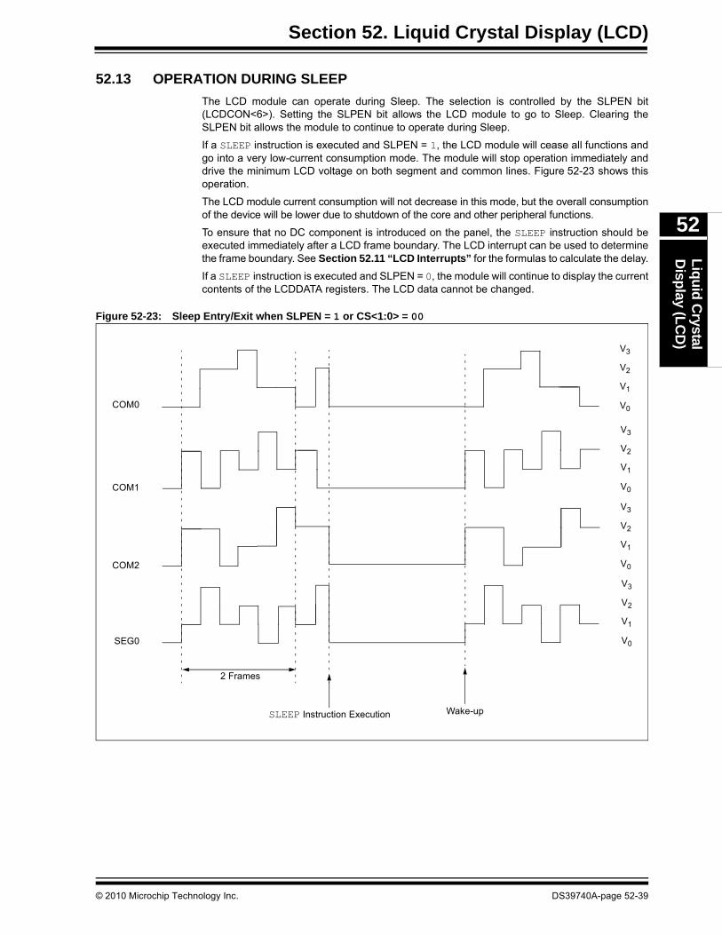
The LCD module can operate during Sleep. The selection is controlled by the SLPEN bit(LCDCON<6>). Setting the SLPEN bit allows the LCD module to go to Sleep. Clearing theSLPEN bit allows the module to continue to operate during Sleep.
If a SLEEP instruction is executed and SLPEN = 1, the LCD module will cease all functions andgo into a very low-current consumption mode. The module will stop operation immediately anddrive the minimum LCD voltage on both segment and common lines. Figure 52-23 shows thisoperation.
The LCD module current consumption will not decrease in this mode, but the overall consumptionof the device will be lower due to shutdown of the core and other peripheral functions.
To ensure that no DC component is introduced on the panel, the SLEEP instruction should beexecuted immediately after a LCD frame boundary. The LCD interrupt can be used to determinethe frame boundary. See Section 52.11 “LCD Interrupts” for the formulas to calculate the delay.
If a SLEEP instruction is executed and SLPEN = 0, the module will continue to display the currentcontents of the LCDDATA registers. The LCD data cannot be changed.
Figure 52-23: Sleep Entry/Exit when SLPEN = 1 or CS<1:0> = 00
SLEEP Instruction Execution Wake-up
2 Frames
V3
V2
V1
V0
V3
V2
V1
V0
V3
V2
V1
V0
V3
V2
V1
V0
COM0
COM1
COM2
SEG0
© 2010 Microchip Technology Inc. DS39740A-page 52-39
PIC
24F F
amily R
eference M
anu
al
DS
39
74
0A
-pa
ge
52
-40
© 2
01
0 M
icroch
ip T
ech
no
log
y Inc.
Bit 4 Bit 3 Bit 2 Bit 1 Bit 0
CS1 CS0 LMUX2 LMUX1 LMUX0
WA r LP2 LP1 LP0
LRLBP0 — LRLAT2 LRLAT1 LRLAT0
BIAS1 BIAS0 MODE13 CKSEL1 CKSEL0
LCDIF — — — —
LCDIE — — — —
— — LCDIP2 LCDIP1 LCDIP0
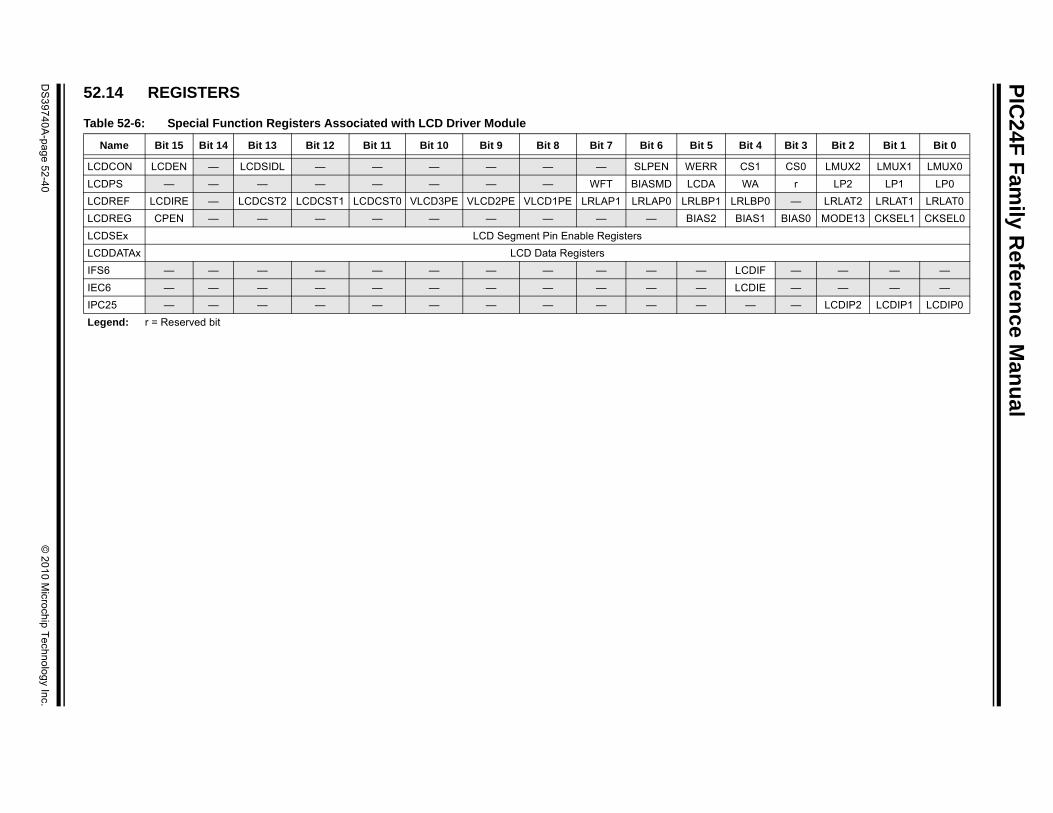
52.14 REGISTERS
Table 52-6: Special Function Registers Associated with LCD Driver Module
Name Bit 15 Bit 14 Bit 13 Bit 12 Bit 11 Bit 10 Bit 9 Bit 8 Bit 7 Bit 6 Bit 5
LCDCON LCDEN — LCDSIDL — — — — — — SLPEN WERR
LCDPS — — — — — — — — WFT BIASMD LCDA
LCDREF LCDIRE — LCDCST2 LCDCST1 LCDCST0 VLCD3PE VLCD2PE VLCD1PE LRLAP1 LRLAP0 LRLBP1
LCDREG CPEN — — — — — — — — — BIAS2
LCDSEx LCD Segment Pin Enable Registers
LCDDATAx LCD Data Registers
IFS6 — — — — — — — — — — —
IEC6 — — — — — — — — — — —
IPC25 — — — — — — — — — — —
Legend: r = Reserved bit
Section 52. Liquid Crystal Display (LCD)L
iqu
id C
rystalD
isplay (L
CD
)
52
52.15 REVISION HISTORY
Revision A (December 2010)
This is the initial released revision of this document.
© 2010 Microchip Technology Inc. DS39740A-page 52-41
PIC24F Family Reference Manual
NOTES:
DS39740A-page 52-42 © 2010 Microchip Technology Inc.
Note the following details of the code protection feature on Microchip devices:
• Microchip products meet the specification contained in their particular Microchip Data Sheet.
• Microchip believes that its family of products is one of the most secure families of its kind on the market today, when used in the intended manner and under normal conditions.
• There are dishonest and possibly illegal methods used to breach the code protection feature. All of these methods, to our knowledge, require using the Microchip products in a manner outside the operating specifications contained in Microchip’s Data Sheets. Most likely, the person doing so is engaged in theft of intellectual property.
• Microchip is willing to work with the customer who is concerned about the integrity of their code.
• Neither Microchip nor any other semiconductor manufacturer can guarantee the security of their code. Code protection does not mean that we are guaranteeing the product as “unbreakable.”
Code protection is constantly evolving. We at Microchip are committed to continuously improving the code protection features of ourproducts. Attempts to break Microchip’s code protection feature may be a violation of the Digital Millennium Copyright Act. If such actsallow unauthorized access to your software or other copyrighted work, you may have a right to sue for relief under that Act.
Information contained in this publication regarding deviceapplications and the like is provided only for your convenienceand may be superseded by updates. It is your responsibility toensure that your application meets with your specifications.MICROCHIP MAKES NO REPRESENTATIONS ORWARRANTIES OF ANY KIND WHETHER EXPRESS ORIMPLIED, WRITTEN OR ORAL, STATUTORY OROTHERWISE, RELATED TO THE INFORMATION,INCLUDING BUT NOT LIMITED TO ITS CONDITION,QUALITY, PERFORMANCE, MERCHANTABILITY ORFITNESS FOR PURPOSE. Microchip disclaims all liabilityarising from this information and its use. Use of Microchipdevices in life support and/or safety applications is entirely atthe buyer’s risk, and the buyer agrees to defend, indemnify andhold harmless Microchip from any and all damages, claims,suits, or expenses resulting from such use. No licenses areconveyed, implicitly or otherwise, under any Microchipintellectual property rights.
2010 Microchip Technology Inc.
Trademarks
The Microchip name and logo, the Microchip logo, dsPIC, KEELOQ, KEELOQ logo, MPLAB, PIC, PICmicro, PICSTART, PIC32 logo, rfPIC and UNI/O are registered trademarks of Microchip Technology Incorporated in the U.S.A. and other countries.
FilterLab, Hampshire, HI-TECH C, Linear Active Thermistor, MXDEV, MXLAB, SEEVAL and The Embedded Control Solutions Company are registered trademarks of Microchip Technology Incorporated in the U.S.A.
Analog-for-the-Digital Age, Application Maestro, CodeGuard, dsPICDEM, dsPICDEM.net, dsPICworks, dsSPEAK, ECAN, ECONOMONITOR, FanSense, HI-TIDE, In-Circuit Serial Programming, ICSP, Mindi, MiWi, MPASM, MPLAB Certified logo, MPLIB, MPLINK, mTouch, Omniscient Code Generation, PICC, PICC-18, PICDEM, PICDEM.net, PICkit, PICtail, REAL ICE, rfLAB, Select Mode, Total Endurance, TSHARC, UniWinDriver, WiperLock and ZENA are trademarks of Microchip Technology Incorporated in the U.S.A. and other countries.
SQTP is a service mark of Microchip Technology Incorporated in the U.S.A.
All other trademarks mentioned herein are property of their respective companies.
© 2010, Microchip Technology Incorporated, Printed in the U.S.A., All Rights Reserved.
Printed on recycled paper.
ISBN: 978-1-60932-758-3
DS39740A-page 52-43
Microchip received ISO/TS-16949:2002 certification for its worldwide headquarters, design and wafer fabrication facilities in Chandler and Tempe, Arizona; Gresham, Oregon and design centers in California and India. The Company’s quality system processes and procedures are for its PIC® MCUs and dsPIC® DSCs, KEELOQ® code hopping devices, Serial EEPROMs, microperipherals, nonvolatile memory and analog products. In addition, Microchip’s quality system for the design and manufacture of development systems is ISO 9001:2000 certified.

DS39740A-page 52-44 2010 Microchip Technology Inc.
AMERICASCorporate Office2355 West Chandler Blvd.Chandler, AZ 85224-6199Tel: 480-792-7200 Fax: 480-792-7277Technical Support: http://support.microchip.comWeb Address: www.microchip.com
AtlantaDuluth, GA Tel: 678-957-9614 Fax: 678-957-1455
BostonWestborough, MA Tel: 774-760-0087 Fax: 774-760-0088
ChicagoItasca, IL Tel: 630-285-0071 Fax: 630-285-0075
ClevelandIndependence, OH Tel: 216-447-0464 Fax: 216-447-0643
DallasAddison, TX Tel: 972-818-7423 Fax: 972-818-2924
DetroitFarmington Hills, MI Tel: 248-538-2250Fax: 248-538-2260
KokomoKokomo, IN Tel: 765-864-8360Fax: 765-864-8387
Los AngelesMission Viejo, CA Tel: 949-462-9523 Fax: 949-462-9608
Santa ClaraSanta Clara, CA Tel: 408-961-6444Fax: 408-961-6445
TorontoMississauga, Ontario, CanadaTel: 905-673-0699 Fax: 905-673-6509
ASIA/PACIFICAsia Pacific OfficeSuites 3707-14, 37th FloorTower 6, The GatewayHarbour City, KowloonHong KongTel: 852-2401-1200Fax: 852-2401-3431
Australia - SydneyTel: 61-2-9868-6733Fax: 61-2-9868-6755
China - BeijingTel: 86-10-8528-2100 Fax: 86-10-8528-2104
China - ChengduTel: 86-28-8665-5511Fax: 86-28-8665-7889
China - ChongqingTel: 86-23-8980-9588Fax: 86-23-8980-9500
China - Hong Kong SARTel: 852-2401-1200 Fax: 852-2401-3431
China - NanjingTel: 86-25-8473-2460Fax: 86-25-8473-2470
China - QingdaoTel: 86-532-8502-7355Fax: 86-532-8502-7205
China - ShanghaiTel: 86-21-5407-5533 Fax: 86-21-5407-5066
China - ShenyangTel: 86-24-2334-2829Fax: 86-24-2334-2393
China - ShenzhenTel: 86-755-8203-2660 Fax: 86-755-8203-1760
China - WuhanTel: 86-27-5980-5300Fax: 86-27-5980-5118
China - XianTel: 86-29-8833-7252Fax: 86-29-8833-7256
China - XiamenTel: 86-592-2388138 Fax: 86-592-2388130
China - ZhuhaiTel: 86-756-3210040 Fax: 86-756-3210049
ASIA/PACIFICIndia - BangaloreTel: 91-80-3090-4444 Fax: 91-80-3090-4123
India - New DelhiTel: 91-11-4160-8631Fax: 91-11-4160-8632
India - PuneTel: 91-20-2566-1512Fax: 91-20-2566-1513
Japan - YokohamaTel: 81-45-471- 6166 Fax: 81-45-471-6122
Korea - DaeguTel: 82-53-744-4301Fax: 82-53-744-4302
Korea - SeoulTel: 82-2-554-7200Fax: 82-2-558-5932 or 82-2-558-5934
Malaysia - Kuala LumpurTel: 60-3-6201-9857Fax: 60-3-6201-9859
Malaysia - PenangTel: 60-4-227-8870Fax: 60-4-227-4068
Philippines - ManilaTel: 63-2-634-9065Fax: 63-2-634-9069
SingaporeTel: 65-6334-8870Fax: 65-6334-8850
Taiwan - Hsin ChuTel: 886-3-6578-300Fax: 886-3-6578-370
Taiwan - KaohsiungTel: 886-7-213-7830Fax: 886-7-330-9305
Taiwan - TaipeiTel: 886-2-2500-6610 Fax: 886-2-2508-0102
Thailand - BangkokTel: 66-2-694-1351Fax: 66-2-694-1350
EUROPEAustria - WelsTel: 43-7242-2244-39Fax: 43-7242-2244-393Denmark - CopenhagenTel: 45-4450-2828 Fax: 45-4485-2829
France - ParisTel: 33-1-69-53-63-20 Fax: 33-1-69-30-90-79
Germany - MunichTel: 49-89-627-144-0 Fax: 49-89-627-144-44
Italy - Milan Tel: 39-0331-742611 Fax: 39-0331-466781
Netherlands - DrunenTel: 31-416-690399 Fax: 31-416-690340
Spain - MadridTel: 34-91-708-08-90Fax: 34-91-708-08-91
UK - WokinghamTel: 44-118-921-5869Fax: 44-118-921-5820
Worldwide Sales and Service
08/04/10