Physics Semiconductors Project
25
9/22/2015 Physics semiconductors project http://www.slideshare.net/AashirwadJindal/physicssemiconductorsproject 1/25 SlideShare Explore Search You Upload Login Signup Search Home Technology Education More Topics For Uploaders Collect Leads Get Started Tips & Tricks Tools For Business Search Semiconductors… Physics Project..
description
Physics Semiconductors Project
Transcript of Physics Semiconductors Project
9/22/2015 Physics semiconductors project
http://www.slideshare.net/AashirwadJindal/physicssemiconductorsproject 1/25
SlideShare Explore Search You
UploadLoginSignup
Search
HomeTechnologyEducationMore Topics
For UploadersCollect Leads
Get Started
Tips & Tricks
Tools
For Business
Search
Semiconductors…Physics Project..
9/22/2015 Physics semiconductors project
http://www.slideshare.net/AashirwadJindal/physicssemiconductorsproject 2/25
4 of 27
1 | p h y s i c s p r o j e c t .
to – heema mam
“If we knewwhat it was we were doing, it would not be called research,
would it?”
― Albert Einstein
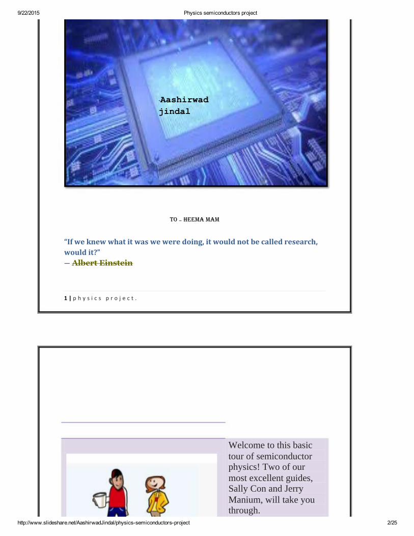
‐Aashirwad
jindal
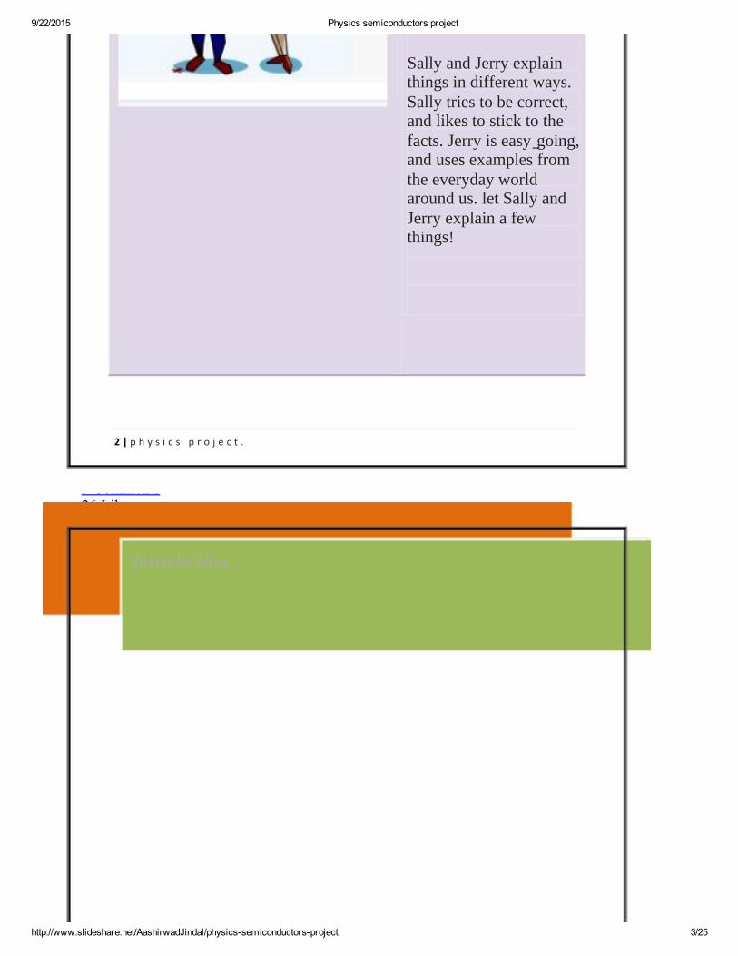
Welcome to this basictour of semiconductorphysics! Two of ourmost excellent guides,Sally Con and JerryManium, will take youthrough.
9/22/2015 Physics semiconductors project
http://www.slideshare.net/AashirwadJindal/physicssemiconductorsproject 3/25
Physics semiconductors project31,640
ShareLikeDownload
Aashirwad Jindal, schooling at schoolFollow0 0 0 0
Published on Jan 31, 2014
its a complete project on semi conductors ...u just ned to save it and have fun its perfect at its
...Published in: Technology, Business
3 Comments26 LikesStatisticsNotes
Full NameComment goes here.12 hours ago Delete Reply Spam BlockAre you sure you want to Yes NoYour message goes here
Share your thoughts...Post
Vishal Trivedi , C.E.O. at Nike@Kshitij Sharma ......Idiot or what you don know how to download!!
2 | p h y s i c s p r o j e c t .
Sally and Jerry explainthings in different ways.Sally tries to be correct,and likes to stick to thefacts. Jerry is easy-going,and uses examples fromthe everyday worldaround us. let Sally andJerry explain a fewthings!
Introduction…
9/22/2015 Physics semiconductors project
http://www.slideshare.net/AashirwadJindal/physicssemiconductorsproject 4/25
3 weeks ago Reply Are you sure you want to Yes NoYour message goes here
Kshitij Sharmaplease allow us to download this.....9 months ago Reply Are you sure you want to Yes NoYour message goes here
Syed Rizwan Yasin , Manager at Android/IOS helpdesk IndianDats a good one bro11 months ago Reply Are you sure you want to Yes NoYour message goes here
aishuapte2 weeks ago
Vishal Trivedi , C.E.O. at Nike3 weeks ago
Jhapranav1 month ago
Harit Sharma2 months ago
vermaakash19993 months ago
Show MoreNo DownloadsViewsTotal Views31,640
3 | p h y s i c s p r o j e c t .
Let's begin this journey into the world of semiconductors with a look atthe history books. In the early 1900s, not much was known of the worldat an atomic level, and even less so at the subatomic level. Physics, to a
large extent, still calmly followed classical rules. But new discoverieslike Röntgen's x-rays, Thomson's electron and Rutherford's discoveryof the atomic nucleus made it clear that new rules were needed. Scientistslike Planck, Einstein, Bohr,Pauli and Heisenberg, to name a few, allcontributed to the development and understanding necessary for thecreation of the new paradigm of quantum physics. The development ofquantum physics also laid the ground for 'Solid State Physics' which is adiscipline explaining the internal atomic structure and the electronicproperties of the materials that we see in our everyday life such as
metals, plastics, glass, etc.
History..
9/22/2015 Physics semiconductors project
http://www.slideshare.net/AashirwadJindal/physicssemiconductorsproject 5/25
On Slideshare0From Embeds0Number of Embeds0ActionsShares0Downloads1,411Comments3Likes26Embeds 0No embeds
No notes for slide
Physics semiconductors project
1. 1. Semiconductors… Physics Project.. Aashirwad jindal to – heema mam “If we knew what it waswe were doing, it would not be called research, would it?” ― Albert Einstein 1|physics project.
2. 2. Welcome to this basic tour of semiconductor physics! Two of our most excellent guides, SallyCon and Jerry Manium, will take you through. Sally and Jerry explain things in different ways.Sally tries to be correct, and likes to stick to the facts. Jerry is easygoing, and uses examples fromthe everyday world around us. let Sally and Jerry explain a few things! 2|physics project.
3. 3. Introduction… 3|physics project.4. 4. History.. Let's begin this journey into the world of semiconductors with a look at the history
books. In the early 1900s, not much was known of the world at an atomic level, and even less so atthe subatomic level. Physics, to a large extent, still calmly followed classical rules. But newdiscoveries like Röntgen's xrays, Thomson's electron and Rutherford's discovery of the atomicnucleus made it clear that new rules were needed. Scientists like Planck, Einstein, Bohr,Pauli andHeisenberg, to name a few, all contributed to the development and understanding necessary for thecreation of the new paradigm of quantum physics. The development of quantum physics also laidthe ground for 'Solid State Physics' which is a discipline explaining the internal atomic structureand the electronic properties of the materials that we see in our everyday life such as metals,plastics, glass, etc. 4|physics project.
5. 5. History.. [Type sidebar content. A sidebar is a standalone supplement to the main document. It isoften aligned on the left or right of the page, or located at the top or bottom. Use the Text BoxTools tab to change the formatting of the sidebar text box.] 5|physics project.
6. 6. Electricity Before we start, it would be a good idea to clarify what electricity is. Electricity canbe seen as a stream of electrons. Electrons are tiny particles with a negative charge. So, roughlyexplained, electricity is a stream of electrons flowing from one point to another. A good way toexplain an electric current passing through a cable would be to imagine a pipe filled with marblesthat exactly fit the pipe. If we push a marble into the pipe in one end, the motion would bedistributed, each marble pushing its neighbor, so that almost instantly a marble in the other endwould be pushed out of the pipe. 6|physics project.
4 | p h y s i c s p r o j e c t .
[Type sidebar content. A sidebar is a standalone supplement to
the main document. It is often aligned on the left or right of the
page, or located at the top or bottom. Use the Text Box Tools tab
to change the formatting of the sidebar text box.]
History..
9/22/2015 Physics semiconductors project
http://www.slideshare.net/AashirwadJindal/physicssemiconductorsproject 6/25
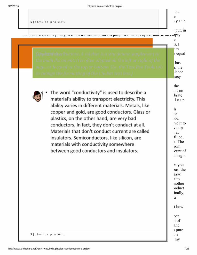
7. 7. Conductivity..!! [Type sidebar content. A sidebar is a standalone supplement to the maindocument. It is often aligned on the left or right of the page, or located at the top or bottom. Usethe Text Box Tools tab to change the formatting of the sidebar text box.] 7|physics project.
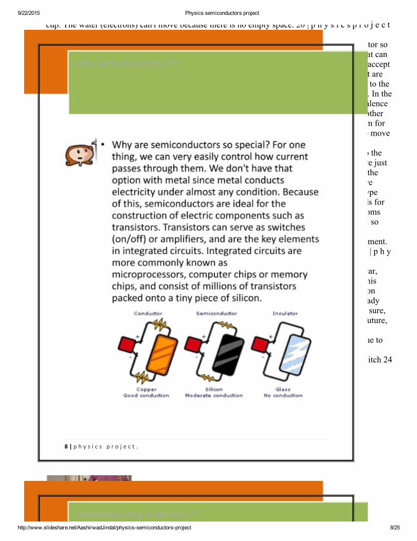
8. 8. Why semiconductors..??? 8|physics project.9. 9. Semiconducting materials..!! Semiconductors can be made of a single material or a combination
of several different materials. In early semiconductor devices germanium was often used. Howeverin today's semiconductor industry, silicon is commonly used. Silicon is very easy to find in Nature.Ordinary sand, like on the beach or in the desert for example, is nothing more than one siliconatom combined with two oxygen atoms. However, if you want silicon in its pure form suitable forthe production of, for instance, computer chips it has to be purified in a carefully monitoredprocess. One of the main reasons for the popularity of silicon is that it is stable and can be heatedto a rather high degree without loosing its material characteristics. This means that engineers canbe sure it will perform according to their plans, even under quite extreme conditions. 9|physicsproject.
10. 10. Semiconducting materials cont…. [Type sidebar content. A sidebar is a standalone supplementto the main document. It is often aligned on the left or right of the page, or located at the top orbottom. Use the Text Box Tools tab to change the formatting of the sidebar text box.] Just to makesure we avoid misunderstandings, when we talk about silicon, we don't mean silicone spelled withan "e" at the end, 'cause that is a material mostly known for its use in human implants. Tounderstand the principles of semiconductors, it is good to first understand the basics of atoms andenergy levels within atoms. So that's where we're going to start. 10 | p h y s i c s p r o j e c t .
11. 11. Silicon and its molecules.. If we look at the solid material of Silicon we will see that it is builtfrom a huge number of Silicon atoms that are brought together. When the atoms interact with eachother, the atomic shells of each atom interacts with the atomic shells of neighboring atoms. On anenergy scale, the overlapping energy shells of all the separate atoms form energy bands that aresimilar to the energy shells in the single atom. Between the bands no electrons are allowed. In asimplified way, it is almost as if the solid material is an enlargement of the single atom. 11 | p h y si c s p r o j e c t .
12. 12. Bands and their theories... To continue our journey, you don't need to fully understand whatSally just said. But what you do need to understand is, that the highest energy band that is occupiedby electrons in a material is called the valence band, just like in the single atom where the highestshell occupied by electrons is called the valence shell. The band with energy one step higher thanthe valence band is theconduction band. The energy gap between these two bands, where noelectrons are allowed, is called the band gap. If you think of the energy bands as steps in a staircasethen the band gap is the area between the steps. You can put your foot on the first step of the stairsand you can put it on the second, but you can never put it 12 | p h y s i c s p r o j e c t .
13. 13. Bands and their theories... cont… somewhere between the first and second. 13 | p h y s i c s p ro j e c t .
14. 14. A electronhole pair..!! A very important feature of the semiconductor material is the electronhole pair. To get a semiconductor to conduct a current, we must make an electron jump from anoccupied to an unoccupied energy level. When it does this it leaves a hole (an empty state). Thishole can be filled by another electron, which itself leaves a new hole. Therefore, we could say thatboth the hole and the electron contribute to the conductivity as they move around in the material.The hole is like a positive charge (lack of negative), the electron is negative. It's a little bit like thissimple puzzle game where you move pieces around to form an image. The moving piecescorrespond to the electrons, of course. 14 | p h y s i c s p r o j e c t .
15. 15. Conduction in different types of materials… As mentioned earlier, the semiconductor has aconducting capacity somewhere between the conductor and the insulator. If we look closer at thematerials we can see why they behave like this. Before we go on, note that contrary to what itsname may suggest, the conduction band is not the only band where conduction of a current may
5 | p h y s i c s p r o j e c t .
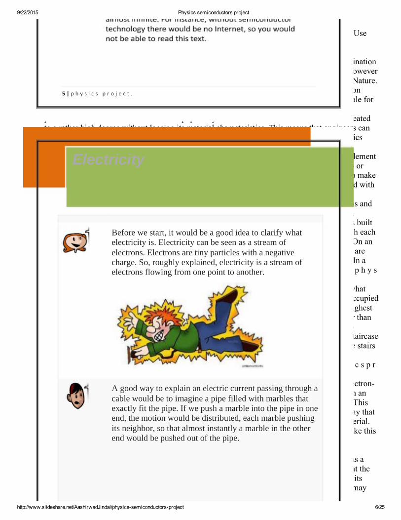
Before we start, it would be a good idea to clarify whatelectricity is. Electricity can be seen as a stream of
electrons. Electrons are tiny particles with a negativecharge. So, roughly explained, electricity is a stream ofelectrons flowing from one point to another.
A good way to explain an electric current passing through a
cable would be to imagine a pipe filled with marbles thatexactly fit the pipe. If we push a marble into the pipe in oneend, the motion would be distributed, each marble pushing
its neighbor, so that almost instantly a marble in the otherend would be pushed out of the pipe.
Electricity
9/22/2015 Physics semiconductors project
http://www.slideshare.net/AashirwadJindal/physicssemiconductorsproject 7/25
occur. Conduction is equally possible in the valence band. In a good conductor like a metal, thehighest energy band with electrons (valence band) is only partially filled. This means that theelectrons can accelerate. In other words, they gain energy so that they can transfer to 15 | p h y s i cs p r o j e c t .
16. 16. Conduction in different types of materials… higher energy levels that are empty. Simply put, ina conductor there is plenty of room for the electrons to jump from an occupied state to an emptyone. If you felt that Sally's explanation of the conduction properties in different materials wascrystal clear, you can skip the following part. But if you're still a little unsure of how it works, Iwill try to show you another way of looking at this phenomenon. To help my explanation, I amgoing to use the unrealistic cup with the waterfilled compartments again. The compartments equalthe energy bands of the material and the water 16 | p h y s i c s p r o j e c t .
17. 17. Conduction in different types of materials… equals the electrons. This time the cup only hastwo compartments, one for the valence band and one for the conduction band. In a conductor, thevalence band is only partially filled. This means that, in our cup, we are going to have the valencecompartment halffilled with water. If we tip the cup from side to side, we will see that it is easyfor the water to move back and forth, just as it is easy for the electrons to move within theconductor. A semiconductor at low temperature is an insulator because there is no place for theelectrons to go to. The valence compartment is filled and no matter how we tip the cup there is noroom for the water to move into. At room temperature, the heat (energy) makes the atoms vibrateslightly, enough for a few of the electrons to break their bonds and jump into the 17 | p h y s i c s pr o j e c t .
18. 18. Conduction in different types of is a standalone [Type sidebar content. A sidebarmaterialscont… supplement to the main document. It is often aligned on the left or right of the page, orlocated at the top or bottom. Use the Text Box Tools tab to change the formatting of the sidebartext box.] conduction band. If we take some water (electrons) from the valence band and move it tothe conduction band, we will have place for the water (electrons) to move in both bands. If we tipour cup, water will move both in the valence and conduction band. Thus, in a semiconductor atroom temperature, a small current will flow. In an insulator, the valence band is completely filled,and as a result no electrons can move. In the cup, no water will move no matter how we tip it. Theband gap between the valence and the conduction band is huge. To move water (electrons) fromour valence compartment to the conduction compartment, we would need to add such an amount ofenergy that our cup (material) would be close to breaking before any water (electrons) would beginto move between the compartments. 18 | p h y s i c s p r o j e c t .
19. 19. Doping … Doping..cont.. Now we are going to talk about doping. Maybe the word makes youthink of athletes taking illegal drugs to perform better. Although doping in sports is outrageous, theparallel between that and doping of semiconductors is not too farfetched. In both cases you havesomething pure, like an athlete or a semiconducting material, and add something foreign to it tochange its performance. So, in the process of doping you add a tiny amount of atoms from anothermaterial to the pure semiconductor. By doing so, you can drastically increase its ability to conducta current. There are two forms of doping, p and n. p stands for positive and n for negative. Finally,two words that are good to know: a pure nondoped semiconductor is called intrinsic, while adoped semiconductor material is called extrinsic. 19 | p h y s i c s p r o j e c t .
20. 20. Pure semiconductors.. Before we look at examples of doped semiconductors, let's look at howthe silicon atoms in pure silicon interact to form the crystal structure of the material. In puresilicon, each atom has four valence electrons and these are shared with four neighboring siliconatoms to make four double bonds. Now each atom will have a completely filled valence shell ofeight electrons. At low temperature this bond is very stable, completely filling the valence bandand thus making conduction impossible. Here is a model of the structure of pure silicon: In a puresemiconductor at low temperature, the valence layer is completely filled with electrons and theconduction band is empty. That would be equal to one filled and one empty compartment in my
6 | p h y s i c s p r o j e c t .
7 | p h y s i c s p r o j e c t .
[Type sidebar content. A sidebar is a standalone supplement to
the main document. It is often aligned on the left or right of the
page, or located at the top or bottom. Use the Text Box Tools tab
to change the formatting of the sidebar text box.]
Conductivity..!!
9/22/2015 Physics semiconductors project
http://www.slideshare.net/AashirwadJindal/physicssemiconductorsproject 8/25
cup. The water (electrons) can't move because there is no empty space. 20 | p h y s i c s p r o j e c t.
21. 21. P doping pdoping is when you add atoms with less valence electrons to the semiconductor sothat the material gets a shortage of electrons in the crystal bonds. This way positive holes that cantransport current are formed. The materials that add holes are called acceptors because they acceptelectrons from the surrounding atoms. In a ptype semiconductor the major carrier of current arethe holes, not the electrons. The p in pdoping stands for positive. This is because compared to theatoms in the semiconductor material the added atoms have fewer negative valence electrons. In thepdoped semiconductor the higher conduction band is empty, but there will be holes in the valenceband. In the cup, this means that we remove some water from the valence compartment. In otherwords, we form air bubbles (positive holes) in the water. Now if we tip the cup, there is room forthe water (electrons) to move in one direction and for the created holes (lack of electrons) to movein the opposite direction (just like bubbles would do in water). 21 | p h y s i c s p r o j e c t .
22. 22. Ndoping… In the process of ndoping you add atoms with one extra valence electron to thepure semiconducting material. This creates a situation where there are extra electrons that are justloosely bound in the crystal. The amount of energy needed to get these electrons to jump to theconduction band so that a current may pass is very small. The materials that add electrons arecalled donors. This is simply because they donate electrons to the semiconductor. In the ntypesemiconductor the major carrier of current is the negative electrons. The n in ndoping stands fornegative. This is because compared to the atoms in the semiconductor material the added atomshave more negative valence electrons. In the ndoped semiconductor, the valence band is full sothere is no room for the electrons to move there. Instead, the extra electrons move into theconduction band. In our cup, we can see that no water will move in the full valence compartment.Instead, the extra water (electrons) added will move within the conduction compartment. 22 | p h ys i c s p r o j e c t .
23. 23. Semiconductorsthe future In a world where computers become faster and faster each year,semiconductor components, like chips and transistors, must be made smaller and smaller. Thismeans that we will eventually reach a limit on how much faster and more effective the Siliconbased technique can be made (in fact, devices operating with just a single electron have alreadybeen demonstrated). "What happens then?" you might ask yourself. Well we don't know for sure,but today's scientists are working hard to find new materials or to improve old ones. In the future,large molecules might do the work that transistors do today. This field is called MolecularElectronics. So hopefully (if you like information technology, that is) computers can continue toevolve for a long time to come. 23 | p h y s i c s p r o j e c t .
24. 24. Circuit diagram… Characteristics of transistor.. Transistor as amplifier. Transistor as switch 24| p h y s i c s p r o j e c t .
25. 25. Circuit diagrams.. Full wave rectifier. half wave rectifier. 25 | p h y s i c s p r o j e c t .26. 26. Circuit diagram… logic gates… Integrated circuit 26 | p h y s i c s p r o j e c t .27. 27. 27 | p h y s i c s p r o j e c t .
RecommendedMore from this author
Managing Project Risk
8 | p h y s i c s p r o j e c t .
Why semiconductors..???
Semiconducting materials..!!
9/22/2015 Physics semiconductors project
http://www.slideshare.net/AashirwadJindal/physicssemiconductorsproject 9/25
Managing Project Schedules
Rescuing Troubled Projects
Physics Investigatory Project Class 12RAHUL247,132
Physics project class 12 EMIsaisathvick102,317
20,000 Students have made physics projects from this list!!Gurpawan Mand36,987
9 | p h y s i c s p r o j e c t .
Semiconductors can be made of a single material ora combination of several different materials. Inearly semiconductor devices germanium was oftenused. However in today's semiconductor industry,silicon is commonly used.
Silicon is very easy to find in Nature. Ordinarysand, like on the beach or in the desert for example,is nothing more than one silicon atom combinedwith two oxygen atoms. However, if you wantsilicon in its pure form suitable for the productionof, for instance, computer chips it has to be purifiedin a carefully monitored process.
One of the main reasons for the popularity of siliconis that it is stable and can be heated to a rather highdegree without loosing its material characteristics.This means that engineers can be sure it willperform according to their plans, even under quiteextreme conditions.
[Type sidebar content. A sidebar is a standalone supplement to
the main document. It is often aligned on the left or right of the
page, or located at the top or bottom. Use the Text Box Tools tab
to change the formatting of the sidebar text box.]
Semiconducting materials cont….
9/22/2015 Physics semiconductors project
http://www.slideshare.net/AashirwadJindal/physicssemiconductorsproject 10/25
physics projectsauravpandey1741,216
CBSE Class XII physics practical project on Metal detectorPranav Ghildiyal24,283
Transformers Project reportTanuj Gupta104,002
Physics projectSri Krishna28,977
12th CBSE Physics Project AC GeneratorAshwin Francis21,658
Physics Investigatory Project on Fluid Mechanicsashrant18,190
10 | p h y s i c s p r o j e c t .
Just to make sure we avoid misunderstandings,when we talk about silicon, we don't mean siliconespelled with an "e" at the end, 'cause that is amaterial mostly known for its use in humanimplants.
To understand the principles of semiconductors, it isgood to first understand the basics of atoms andenergy levels within atoms. So that's where we'regoing to start.
If we look at the solid material of Silicon we will seethat it is built from a huge number of Silicon atoms
Silicon and its molecules..
9/22/2015 Physics semiconductors project
http://www.slideshare.net/AashirwadJindal/physicssemiconductorsproject 11/25
Physics investigatory projectmihika1343,059
Semiconductor physicsspeaking technology10,118
Optical fibers physics projectmenna9410,105
Physics projectJayashree Venkatesh7,223
Chemistry Investigatory Project Class 12RAHUL125,087
Semiconductor Devices Class 12 Part1RAHUL5,746
11 | p h y s i c s p r o j e c t .
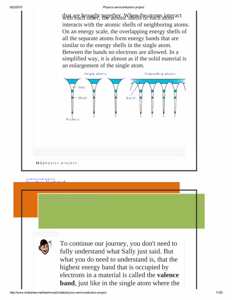
that are brought together. When the atoms interactwith each other, the atomic shells of each atominteracts with the atomic shells of neighboring atoms.On an energy scale, the overlapping energy shells ofall the separate atoms form energy bands that aresimilar to the energy shells in the single atom.Between the bands no electrons are allowed. In asimplified way, it is almost as if the solid material isan enlargement of the single atom.
To continue our journey, you don't need tofully understand what Sally just said. But
what you do need to understand is, that thehighest energy band that is occupied byelectrons in a material is called the valenceband, just like in the single atom where the
Bands and their theories...
9/22/2015 Physics semiconductors project
http://www.slideshare.net/AashirwadJindal/physicssemiconductorsproject 12/25
Foootbal physical educationAashirwad Jindal10,554
mettalurgy12th sci cbseAashirwad Jindal442
ENGLISHEnglishFrançaisEspañolPortuguês (Brasil)Deutsch
EnglishEspanolPortuguesFrançaisDeutsche
AboutDev & APIBlogTermsPrivacyCopyrightSupport
12 | p h y s i c s p r o j e c t .
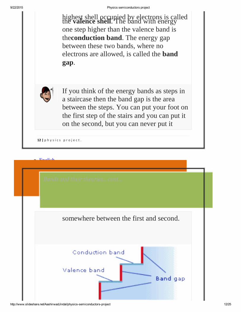
highest shell occupied by electrons is calledthe valence shell. The band with energyone step higher than the valence band is
theconduction band. The energy gapbetween these two bands, where noelectrons are allowed, is called the bandgap.
If you think of the energy bands as steps ina staircase then the band gap is the areabetween the steps. You can put your foot on
the first step of the stairs and you can put iton the second, but you can never put it
somewhere between the first and second.
Bands and their theories... cont…
9/22/2015 Physics semiconductors project
http://www.slideshare.net/AashirwadJindal/physicssemiconductorsproject 13/25
LinkedIn Corporation © 2015
×
Share Clipboard
×
Enter email addresses
From Add a message
SendEmail sent successfully..
FacebookTwitterLinkedInGoogle+
Link
Public clipboards featuring this slide
×
No public clipboards found for this slide
13 | p h y s i c s p r o j e c t .
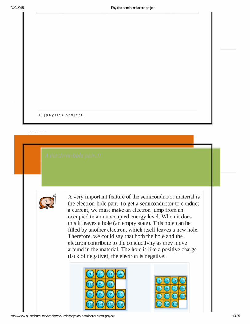
A very important feature of the semiconductor material isthe electron-hole pair. To get a semiconductor to conducta current, we must make an electron jump from anoccupied to an unoccupied energy level. When it doesthis it leaves a hole (an empty state). This hole can befilled by another electron, which itself leaves a new hole.Therefore, we could say that both the hole and theelectron contribute to the conductivity as they movearound in the material. The hole is like a positive charge(lack of negative), the electron is negative.
A electronhole pair..!!
9/22/2015 Physics semiconductors project
http://www.slideshare.net/AashirwadJindal/physicssemiconductorsproject 14/25
14 | p h y s i c s p r o j e c t .
It's a little bit like this simple puzzle game where youmove pieces around to form an image. The moving piecescorrespond to the electrons, of course.
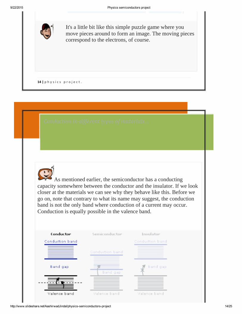
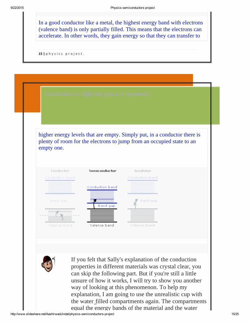
As mentioned earlier, the semiconductor has a conductingcapacity somewhere between the conductor and the insulator. If we lookcloser at the materials we can see why they behave like this. Before wego on, note that contrary to what its name may suggest, the conductionband is not the only band where conduction of a current may occur.Conduction is equally possible in the valence band.
Conduction in different types of materials…
9/22/2015 Physics semiconductors project
http://www.slideshare.net/AashirwadJindal/physicssemiconductorsproject 15/25
15 | p h y s i c s p r o j e c t .
In a good conductor like a metal, the highest energy band with electrons(valence band) is only partially filled. This means that the electrons canaccelerate. In other words, they gain energy so that they can transfer to
higher energy levels that are empty. Simply put, in a conductor there isplenty of room for the electrons to jump from an occupied state to anempty one.
If you felt that Sally's explanation of the conductionproperties in different materials was crystal clear, youcan skip the following part. But if you're still a littleunsure of how it works, I will try to show you anotherway of looking at this phenomenon. To help myexplanation, I am going to use the unrealistic cup withthe water-filled compartments again. The compartmentsequal the energy bands of the material and the water
Conduction in different types of materials…Conduction in different types of materials…Conduction in different types of materials…
9/22/2015 Physics semiconductors project
http://www.slideshare.net/AashirwadJindal/physicssemiconductorsproject 16/25
16 | p h y s i c s p r o j e c t .
equal the energy bands of the material and the water
17 | p h y s i c s p r o j e c t .
equals the electrons. This time the cup only has twocompartments, one for the valence band and one for theconduction band.
In a conductor, the valence band is only partiallyfilled. This means that, in our cup, we are going tohave the valence compartment half-filled with water.If we tip the cup from side to side, we will see that itis easy for the water to move back and forth, just as itis easy for the electrons to move within theconductor.
A semiconductor at low temperature is an insulatorbecause there is no place for the electrons to go to.The valence compartment is filled and no matter howwe tip the cup there is no room for the water to moveinto. At room temperature, the heat (energy) makesthe atoms vibrate slightly, enough for a few of theelectrons to break their bonds and jump into the
Conduction in different types of materials…
9/22/2015 Physics semiconductors project
http://www.slideshare.net/AashirwadJindal/physicssemiconductorsproject 17/25
18 | p h y s i c s p r o j e c t .
conduction band. If we take some water (electrons)from the valence band and move it to the conductionband, we will have place for the water (electrons) tomove in both bands. If we tip our cup, water willmove both in the valence and conduction band. Thus,in a semiconductor at room temperature, a smallcurrent will flow.
In an insulator, the valence band is completely filled,and as a result no electrons can move. In the cup, nowater will move no matter how we tip it. The bandgap between the valence and the conduction band ishuge. To move water (electrons) from our valencecompartment to the conduction compartment, wewould need to add such an amount of energy that ourcup (material) would be close to breaking before anywater (electrons) would begin to move between thecompartments.
[Type sidebar content. A sidebar is a standalone supplement to
the main document. It is often aligned on the left or right of the
page, or located at the top or bottom. Use the Text Box Tools tab
to change the formatting of the sidebar text box.]
Conduction in different types of materials cont…
Doping …Doping..cont..
9/22/2015 Physics semiconductors project
http://www.slideshare.net/AashirwadJindal/physicssemiconductorsproject 18/25
19 | p h y s i c s p r o j e c t .
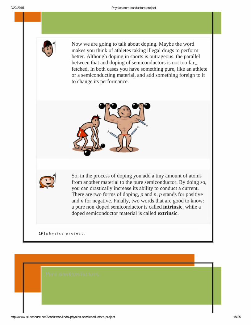
Now we are going to talk about doping. Maybe the word
makes you think of athletes taking illegal drugs to performbetter. Although doping in sports is outrageous, the parallelbetween that and doping of semiconductors is not too far-fetched. In both cases you have something pure, like an athleteor a semiconducting material, and add something foreign to it
to change its performance.
So, in the process of doping you add a tiny amount of atoms
from another material to the pure semiconductor. By doing so,you can drastically increase its ability to conduct a current.There are two forms of doping, p and n. p stands for positive
and n for negative. Finally, two words that are good to know:a pure non-doped semiconductor is called intrinsic, while a
doped semiconductor material is called extrinsic.
Pure semiconductors..
9/22/2015 Physics semiconductors project
http://www.slideshare.net/AashirwadJindal/physicssemiconductorsproject 19/25
20 | p h y s i c s p r o j e c t .
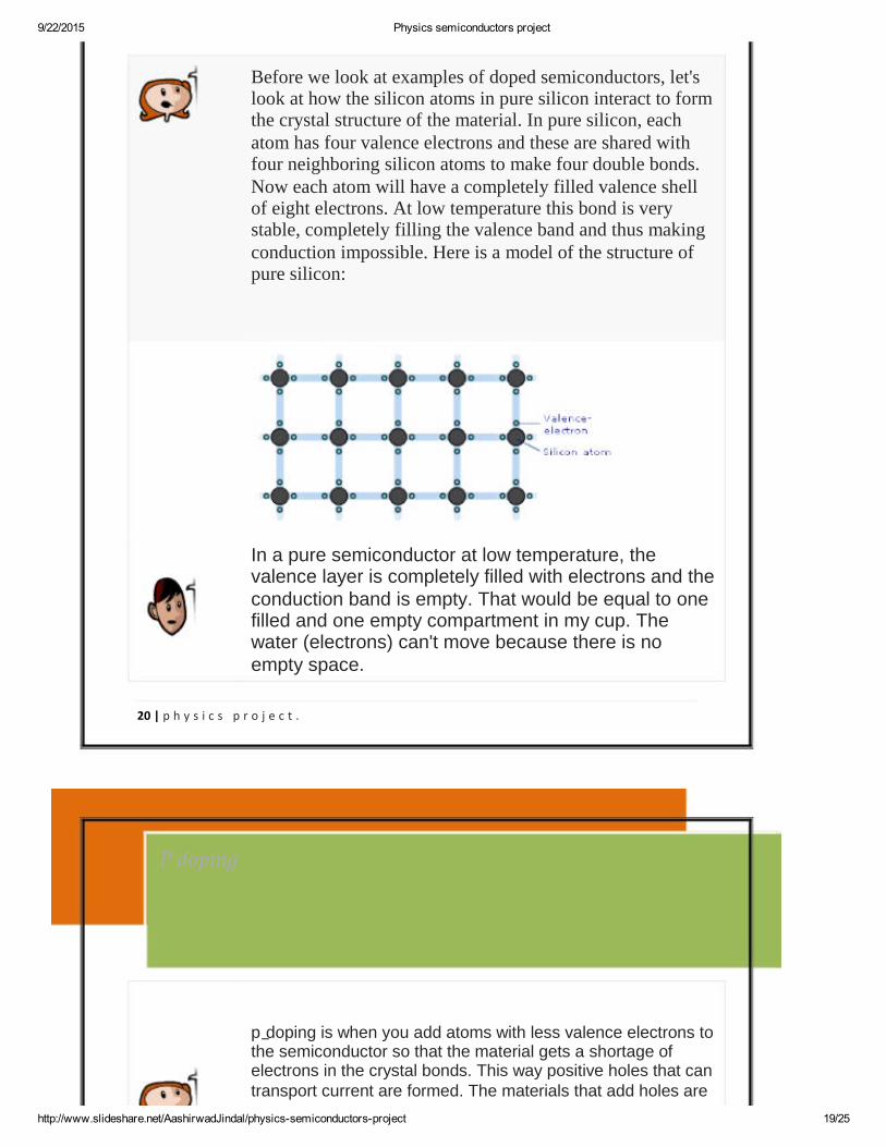
Before we look at examples of doped semiconductors, let'slook at how the silicon atoms in pure silicon interact to formthe crystal structure of the material. In pure silicon, each
atom has four valence electrons and these are shared withfour neighboring silicon atoms to make four double bonds.
Now each atom will have a completely filled valence shellof eight electrons. At low temperature this bond is verystable, completely filling the valence band and thus making
conduction impossible. Here is a model of the structure ofpure silicon:
In a pure semiconductor at low temperature, thevalence layer is completely filled with electrons and theconduction band is empty. That would be equal to onefilled and one empty compartment in my cup. Thewater (electrons) can't move because there is noempty space.
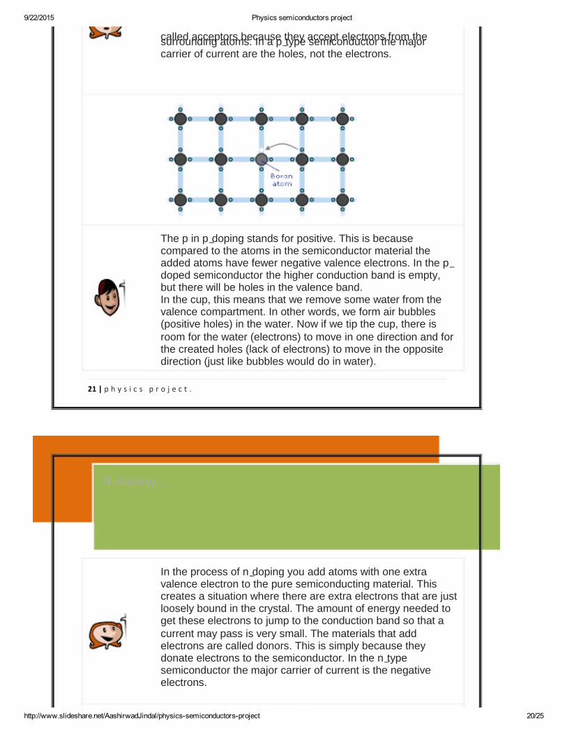
p-doping is when you add atoms with less valence electrons tothe semiconductor so that the material gets a shortage ofelectrons in the crystal bonds. This way positive holes that cantransport current are formed. The materials that add holes are
P doping
9/22/2015 Physics semiconductors project
http://www.slideshare.net/AashirwadJindal/physicssemiconductorsproject 20/25
21 | p h y s i c s p r o j e c t .
called acceptors because they accept electrons from thesurrounding atoms. In a p-type semiconductor the majorcarrier of current are the holes, not the electrons.
The p in p-doping stands for positive. This is becausecompared to the atoms in the semiconductor material theadded atoms have fewer negative valence electrons. In the p-doped semiconductor the higher conduction band is empty,but there will be holes in the valence band.In the cup, this means that we remove some water from thevalence compartment. In other words, we form air bubbles(positive holes) in the water. Now if we tip the cup, there isroom for the water (electrons) to move in one direction and forthe created holes (lack of electrons) to move in the oppositedirection (just like bubbles would do in water).
In the process of n-doping you add atoms with one extravalence electron to the pure semiconducting material. Thiscreates a situation where there are extra electrons that are justloosely bound in the crystal. The amount of energy needed toget these electrons to jump to the conduction band so that acurrent may pass is very small. The materials that addelectrons are called donors. This is simply because theydonate electrons to the semiconductor. In the n-typesemiconductor the major carrier of current is the negativeelectrons.
Ndoping…
9/22/2015 Physics semiconductors project
http://www.slideshare.net/AashirwadJindal/physicssemiconductorsproject 21/25
22 | p h y s i c s p r o j e c t .
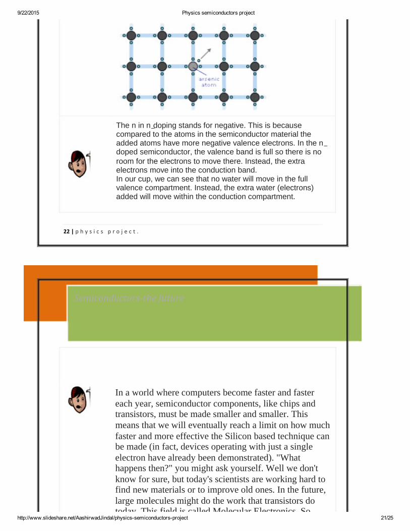
The n in n-doping stands for negative. This is becausecompared to the atoms in the semiconductor material theadded atoms have more negative valence electrons. In the n-doped semiconductor, the valence band is full so there is noroom for the electrons to move there. Instead, the extraelectrons move into the conduction band.In our cup, we can see that no water will move in the fullvalence compartment. Instead, the extra water (electrons)added will move within the conduction compartment.
In a world where computers become faster and fastereach year, semiconductor components, like chips andtransistors, must be made smaller and smaller. Thismeans that we will eventually reach a limit on how muchfaster and more effective the Silicon based technique canbe made (in fact, devices operating with just a singleelectron have already been demonstrated). "Whathappens then?" you might ask yourself. Well we don'tknow for sure, but today's scientists are working hard tofind new materials or to improve old ones. In the future,large molecules might do the work that transistors dotoday. This field is called Molecular Electronics. So
Semiconductorsthe future
9/22/2015 Physics semiconductors project
http://www.slideshare.net/AashirwadJindal/physicssemiconductorsproject 22/25
23 | p h y s i c s p r o j e c t .
today. This field is called Molecular Electronics. Sohopefully (if you like information technology, that is)computers can continue to evolve for a long time tocome.
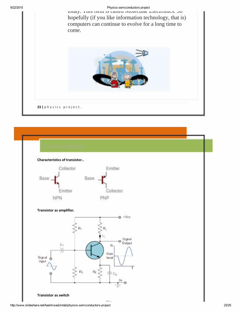
Characteristics of transistor..
Transistor as amplifier.
Transistor as switch
Circuit diagram…
9/22/2015 Physics semiconductors project
http://www.slideshare.net/AashirwadJindal/physicssemiconductorsproject 23/25
24 | p h y s i c s p r o j e c t .
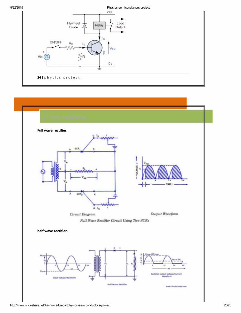
Full wave rectifier.
half wave rectifier.
Circuit diagrams..
9/22/2015 Physics semiconductors project
http://www.slideshare.net/AashirwadJindal/physicssemiconductorsproject 24/25
25 | p h y s i c s p r o j e c t .
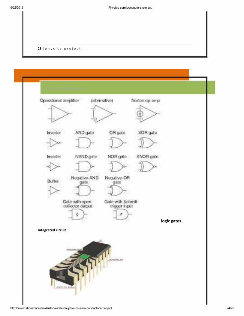
logic gates…
Integrated circuit
Circuit diagram…

9/22/2015 Physics semiconductors project
http://www.slideshare.net/AashirwadJindal/physicssemiconductorsproject 25/25
26 | p h y s i c s p r o j e c t .
27 | p h y s i c s p r o j e c t .