Physics of Semiconductor Devices Chapter 4:...
25
2006-04-05 Ulf Lindefelt, ITM, MIUN 1 Physics of Semiconductor Devices – Chapter 4: Thyristors • 4.1: Introduction • 4.2: Basic characteristics • 4.3: Shockley diode and three-terminal thyristor • 4.4: Related power thyristors • 4.5: Diac and triac • 4.6: Unijunction transistor and trigger thyristor • 4.7: Field-controlled thyristor Student presentations
Transcript of Physics of Semiconductor Devices Chapter 4:...
2006-04-05 Ulf Lindefelt, ITM, MIUN 1
Physics of Semiconductor Devices –
Chapter 4: Thyristors
• 4.1: Introduction
• 4.2: Basic characteristics
• 4.3: Shockley diode and three-terminal thyristor
• 4.4: Related power thyristors
• 4.5: Diac and triac
• 4.6: Unijunction transistor and trigger thyristor
• 4.7: Field-controlled thyristor
Student
presentations

2006-04-05 Ulf Lindefelt, ITM, MIUN 2
4.1: Introduction
• The word “thyristor” comes from the word “gas thyratron”, which was an old-fashioned gas-based device having roughly the same electrical characteristics as the semiconductor-based thyristor.
• Basically, a thyristor is a switch which has a forward high impedance low current OFF state and a forward low impedance high current ON state.
• In general terms a thyristor is a semiconductor device of the type pnpn or npnp, i.e., a four-layer device. A two-terminal thyristor is often called a Shockley diode.
• A theoretical description of how a thyrisor works was developed by Moll et al. (J.L. Moll, M. Tanenbaum, J.M. „Goldley and N. Holonyak, “p-n-p-n Transistor Switches”, Proc. IRE 44, 1174 (1956)).
• It is typically used in the high voltage, high current regime (typically 10 kV, 5kA)

2006-04-05 Ulf Lindefelt, ITM, MIUN 3
4.2: Basic characteristics
Fig.2a: Typical doping profiles in
a thyristor
Shockley
diode
Thyristor
In these lectures I use the
term „thyristor‟ to denote
also the „Shockley diode‟

2006-04-05 Ulf Lindefelt, ITM, MIUN 4
4.2: Basic characteristics
• (0)-(1): Forward blocking (or OFF)
state
• (1): Forward breakover (at
breakover voltage VBF and
switching current Is)
• (1)-(2): Negative resistance region
• (2): Holding state (at holding
voltage Vh and holding current Ih)
• (2)-(3): Forward conducting (or
ON) state
• (0)-(4): Reverse blocking state
• (4)-(5): Reverse breakdown state

2006-04-05 Ulf Lindefelt, ITM, MIUN 5
Forward OFF, breakover and ON
(a) In equilibrium
(b) In the forward OFF-state: J1 and J3 are forward biased, J2 is reverse biased
(c) In the forward ON state: All junctions are forward biased
Between forward OFF state and forward ON state, there is a breakover point (besides the negative resistance region and holding state), which will be investigated next.

2006-04-05 Ulf Lindefelt, ITM, MIUN 6
Analysis of forward OFF and forward breakover
(a model borrowed from transistors)
A thyristor can be partitioned into
two closely coupled transistors,
one npn and one pnp
Resulting transistor
equivalent

2006-04-05 Ulf Lindefelt, ITM, MIUN 7
Analysis of forward OFF and forward breakover
From the transistor model we get
1 1 1(1 )B A COI I I
1 2Since (see fig)B CI I
2 2 2C K COI I I
Leakage
currents
1 1 2 2(1 ) A CO K COI I I I
Furthermore, since
we getA g KI I I
2 1 2
1 21 ( )
g CO CO
A
I I II
1 and 2 are increasing functions
of IA, such that they are small for
small IA and (1+2) approaches unity
for larger currents. Thus IA grows,
giving rise to forward breakover.
This model describes the forward OFF
state up to forward breakover. It results
in a regenerative behaviour (amplification
in the constituent transistors).

2006-04-05 Ulf Lindefelt, ITM, MIUN 8
Analysis of forward OFF and forward breakover
From the expression just derived,
we find that
This instability at breakover may
result in a large anode current
not only caused by a small gate
current (as in this derivation), but
also by a slight increase in tempera-
ture.
The forward breakover point can also
be obtained by assuming that the
junction J2 starts to go into ava-
lanche (see the book, p.205-206).
There an expression is derived for
the forwared breakover voltage VBF:
where n is a constant (approx. 4-6)
and VB is the breakdown voltage at
the junction J1.
Again, the importance of the
expression (1-1-2) and its role in
describing the instability at forward
breakover is evident.
2 1 2
1 21 ( )
g CO CO
A
I I II
2
1 21 ( )
A
g
dI
dI
1/
1 2(1 ) n
BF BV V

2006-04-05 Ulf Lindefelt, ITM, MIUN 9
Analysis of forward ON state
p n p n
n
n≈ p
p
n,p
Analogous to
a pin diode
“Hammock”
The high electron-hole concentration
floods J2, screening out the electric field
from the ionized dopants, thereby reducing
the reverse bias.

2006-04-05 Ulf Lindefelt, ITM, MIUN 10
Analysis of forward ON state
• The effects of lifetime
• Let t denote the electron/hole lifetime when n≈ p: R = n/t.
• For large life times, a high density electron-hole plasma can be built
up and the large concentration of charge carriers gives a high
current for a given potential drop across the thyristor.
• For small lifetimes, only a low density electron-hole plasma can be
built up, resulting in a relatively low current for a given potential drop
across the thyristor.

2011-05-10 Ulf Lindefelt, ITM, MIUN 11
Reverse blocking and breakdown voltage
• Under reverse blocking, junctions J1 and J3 are reverse biased.
• Breakdown (i.e., large reverse current) happens either if J1 goes into avalanche or if the depletion region reaches the junction J2 (punch through)
• In the latter case holes in the p2 region diffuse to J2 and is accelerated by the strong electric field in the depletion region. When they reach the p1 region, elec-trons are pulled in from the contact. In this way a large current is set up in the reverse direction.
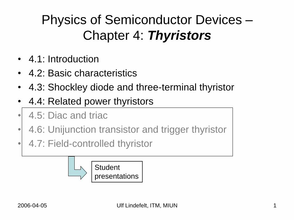
2011-05-11 Ulf Lindefelt, ITM, MIUN 12
Reaching for high breakdown voltages: Beveled structures
• Typical high-voltage high-current
(=power) thyristors look like CD-discs
(without the hole in the middle).
• By choosing appropriate doping and
n1-layer thickness, high breakdown
voltages inside the thyristor can be
achieved.
• On the (circular) edge, however,
breakdown in the air can take place at
much lower voltages.
• To avoid this, different types of edge
profiles can be used (beveled edges).
• By using beveled structures, the
surface field Es can be lowered
significantly compared to the bulk field
Eb, ensuring that the breakdown will
occur uniformly in the bulk.
Es
Eb

2006-04-05 Ulf Lindefelt, ITM, MIUN 13
4.3.1: Thyristor Turn-On
Ways to turn on a thyristor are
• Voltage triggering
– Slowly increasing the anode
current to pass the holding current
(see figure on the right)
– High dV/dt
• Gate current triggering
• Light triggering

2006-04-05 Ulf Lindefelt, ITM, MIUN 14
Thyristor Turn-On
• High dV/dt, i.e., rapid increase of the voltage across the thyristor
• When the voltage is suddenly
increased, so that almost no
recombination has time to take place,
„all‟ holes injected from A and „all‟
electrons from K diffuse to the reverse-
biased junction J2, flooding this
junction and thereby reducing the
reverse bias, starting a forward ON
current.
• Alternatively, the large current associ-
ated with the rapid motion of charge
makes the sum of the alphas approach
unity, thereby turning on the thyristor.
• This may reduce the breakover
voltage to half or less of its static
value.
Forward OFF
Holes
Electrons

2011-05-11 Ulf Lindefelt, ITM, MIUN 15
Thyristor Turn-On
• Gate current triggering
• With a positive gate voltage on the p2 layer for a thyristor in the forward OFF state, the reverse bias in the junction J2 can be reduced considerably, increasing the thyristor current considerably.
• In addition, this increase in thyristor current makes the sum of the alphas approach unity:
• The thyristor is turned ON.
• The GTO (Gate Turn Off Thyristor) works in this way.
Forward OFF
2 1 2
1 21 ( )
g CO CO
A
I I II
Forward ON

2006-04-05 Ulf Lindefelt, ITM, MIUN 16
Thyristor Turn-On
• Turn-on characteristics when a
gate current Ig is applied at time
zero
• The figure shows the delay in time
before the thyristor is fully turned
ON.

2006-04-05 Ulf Lindefelt, ITM, MIUN 17
Thyristor Turn-On
• Light triggering
• If light of appropriate energy hits
the reverse biased junction J2, the
generated electrons will move to
the n1 side and the generated
holes will move to the p2 side.
• This creates an electric field which
counteracts the forward OFF state
reverse bias (at J2), and a current
will begin to flow.
• For the same reason as for a gate
current triggered thyristor, the
thyristor goes into its forward ON
state.
E
E
E’
2011-05-10 Ulf Lindefelt, ITM, MIUN 18
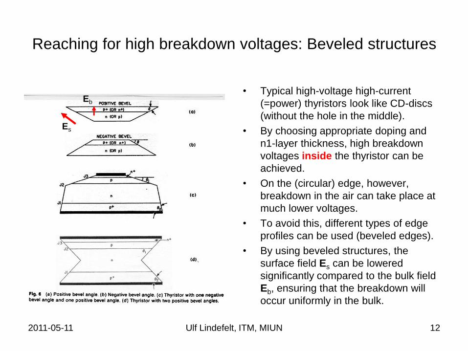
Thyristor Turn-Off
• To turn off the thyristor, the electron-hole plasma in it must either be made to disappear through recombination or be pulled out from the device (through the contacts).
Ways to turn off a thyristor are:
• Reducing the current below the holding current
• Reversing the anode current below zero (current controlled turn off)
– Charge pulled out through the anode-cathode contacts + recombination
• Changing the polarity of the voltage (voltage controlled turn off)
– Charge pull out + recombination
• Applying a negative gate voltage– Charge pulled out through the gate +
recombination
– The junction J3 is forced to become reverse biased, thus opposing injection of electrons into the device.
n
n≈ p
p
n,p
p n p n
-
A GTO (Gate Turn-off) thyristor can
be both turned on and turned off with
a gate electrode.
2011-05-11 Ulf Lindefelt, ITM, MIUN 19
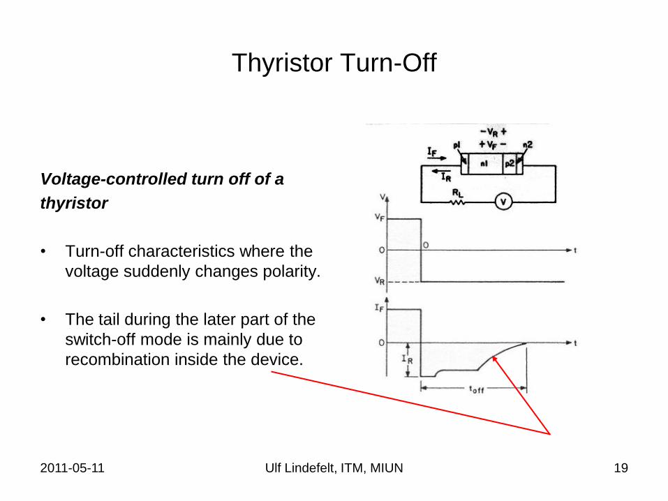
Thyristor Turn-Off
Voltage-controlled turn off of a
thyristor
• Turn-off characteristics where the
voltage suddenly changes polarity.
• The tail during the later part of the
switch-off mode is mainly due to
recombination inside the device.
2006-04-05 Ulf Lindefelt, ITM, MIUN 20
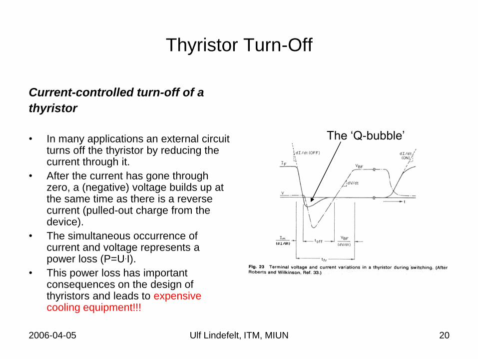
Thyristor Turn-Off
Current-controlled turn-off of a
thyristor
• In many applications an external circuit turns off the thyristor by reducing the current through it.
• After the current has gone through zero, a (negative) voltage builds up at the same time as there is a reverse current (pulled-out charge from the device).
• The simultaneous occurrence of current and voltage represents a power loss (P=U.I).
• This power loss has important consequences on the design of thyristors and leads to expensive cooling equipment!!!
The „Q-bubble‟

2006-04-05 Ulf Lindefelt, ITM, MIUN 21
A common application of thyristors
• The load may for instance be a
light bulb or a heater
• If the turn-on gate current pulses
are delivered near the beginning
of each cycle, more power is
delivered to the load.
• If the gate current pulses are
delayed, the thyristor will not turn
on until later in the cycle, and less
power will be delivered to the load.
• One common aplication of
thyristors is as „dimmers‟.
2006-04-05 Ulf Lindefelt, ITM, MIUN 22
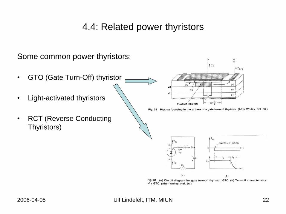
4.4: Related power thyristors
Some common power thyristors:
• GTO (Gate Turn-Off) thyristor
• Light-activated thyristors
• RCT (Reverse Conducting
Thyristors)

2006-04-05 Ulf Lindefelt, ITM, MIUN 23
4.4: Related power thyristors
• Light-triggered (or light activated)
thyristor

2006-04-05 Ulf Lindefelt, ITM, MIUN 24
4.4: Related power thyristors
Reverse Conducting Thyristor
(RCT)
• Both the anode and cathode are
shorted.
• When the RCT is in the reverse
bias, the electrons (holes) on the
anode (cathode) side enter the
device through the n+ (p) region
between the p- (n-) type islands.
• Hence, no reverse biased junction
stops the current, and the RCT
can conduct in both directions.

2006-04-05 Ulf Lindefelt, ITM, MIUN 25
Student Tasks
Make a lecture presentation for your fellow students on one of the following topics:
1. The diac (diode ac switch)
2. The triac (triode ac switch)
3. The UJT (unijunction transistor)
4. The PUT (programmable unijunction transistor), SUS (silicon unilateral switch), and SBS (silicon bilateral switch)
5. The FCT (field-controlled thyristor)
Try to explain the physics behind the functioning of the devices!


![MOSFETs [CHAPTER 6]apachepersonal.miun.se/~gorthu/device/Omi.pdfmicrowave amplifiers •Higher input impedance than bipolar transistors •Thermally stable Negative temperature coefficient](https://static.fdocuments.in/doc/165x107/5e3a4e73b69ac32a5040b7b5/mosfets-chapter-6-gorthudeviceomipdf-microwave-amplifiers-ahigher-input-impedance.jpg)