
Physical Properties of Carbon...
14
Physical Properties of Carbon Nanotubes Ao Teng Course: Solid State II Instructor: Elbio Dagotto Spring 2010 Department of Physics University of Tennessee Email: [email protected]
Transcript of Physical Properties of Carbon...
Physical Properties of Carbon Nanotubes
Ao Teng
Course: Solid State II Instructor: Elbio Dagotto Spring 2010 Department of Physics University of Tennessee Email: [email protected]

Physical Properties of Carbon Nanotubes
Abstract:
Carbon nanotubes, as the prototypes of artificial one dimensional nano materials, have been intensely investigated since 1991. They originated from graphite sheets, but come along with some new physical properties due to quantum confinement. Soon after they were discovered, researchers realized their broad applications in prospect. In this paper, a brief introduction focusing on basic concepts and geometry of carbon nanotubes will be conducted, followed by a series of discussions on related electronic properties of carbon nanotubes, as well as other physical properties. Contents: I. Introduction II. Typical Synthesis Methods of Carbon Nanotubes A. Electric-Arc Discharge Technique B. Chemical Vapor Deposition III. Structure and Symmetry of Carbon Nanotubes IV. Electronic Properties of Carbon Nanotubes A. Reciprocal space and Brillouin zone B. Tight-binding model and band structure C. Zone-folding approximation and metallicity D. Density of states (DOS) and Van Hove singularities V. Other Physical Properties and Applications I. Introduction Physics down to the scale of nanometers has been a fascinating field for quite a long time, even back to more than 50 years ago, Richard Feynman realized that ”There’s Plenty of Room at the Bottom”[1] and predicted that nano science would be a new frontier. Multiwalled carbon nanotubes (MWNT), as hollow cylinders with diameters in the nanometer range,

consisting of carbon atoms, were first observed in 1991 by Sumio Iijima at the NEC Research Laboratory, when he studied the soot made from by-products obtained during the synthesis of fullerenes by the electric arc discharge method. [2] Two years later, single-wall carbon nanotubes (SWNT) were synthesized. [3][4] II. Typical Synthesis Methods of Carbon Nanotubes Generally, synthesis methods of carbon nanotubes can be classified into two main categories corresponding to different temperatures: The high temperature routes, such as the electric-arc discharge technique; the medium temperature routes (the most popular one is chemical vapor deposition). A. Electric-Arc Discharge Technique An electric-arc discharge is an electrical breakdown of a gas which produces an ongoing plasma, resulting from a current flowing through normally nonconductive media. In Iijima’s initial experiment [2], he used a DC arc discharge in argon consisting of a set of carbon electrodes running at 2000-3000˚C at nominal conditions of 100A and 20V. The modified version of this method could bring the temperature up to 6000˚C and make the graphite to sublimate. As a consequence, carbon atoms are ejected from the solid and form plasma. These atoms will accumulate on the cathode, which is relatively colder. If small amounts of transition metals are introduced in the target graphite, the single-walled carbon nanotubes are the dominant product, otherwise formation of multiwalled carbon nanotubes will take place.
Fig. 1. Left: Plasma from the electric-arc experiment performed by Thomas Ebbesen et al. [5] Middle: 2 sheets carbon nanotube, adapted from Iijima’s paper [2]. Right: By printing patterns of catalyst particles on the substrate, Hongjie Dai et al. have been able to control where the tubes form with chemical vapor deposition method. [5]

B. Chemical Vapor Deposition With transition-metal particles as growth germs, the carbon containing gaseous compounds at temperature 600-1100˚C will decompose on those sites and form carbon filaments of various sizes and shapes including nanotubes. Typical compounds are carbon monoxide or hydrocarbons. III. Structure and Symmetry of Carbon Nanotubes The topological structure of SWNT is quite like modified single sheet graphene, thus the tubes are usually labeled in terms of the graphene lattice vectors.
Fig. 2.Graphene lattice vectors a1 and a2. The chiral vector Ch=5a1+3a2 represents a possible wrapping of the two-dimensional graphene sheet into a tubular form. The direction perpendicular to Ch is the tube axis. The chiral angle 𝜃𝜃 is defined by the Ch vector and the a1 zigzag direction of the graphene lattice. In the present example, a (5, 3) nanotube is under construction and the resulting tube is illustrated below. [6]
Fig.3.Atomic structures of (12, 0) zigzag, (6, 6) armchair, and (6, 4) chiral nanotubes.
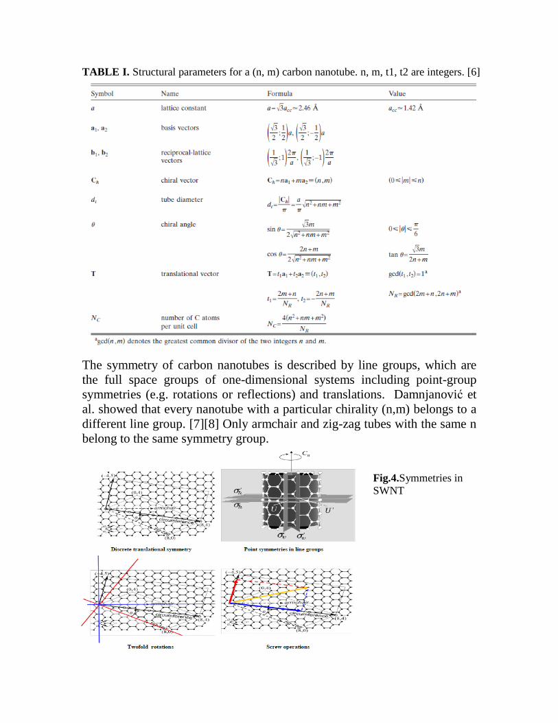
TABLE I. Structural parameters for a (n, m) carbon nanotube. n, m, t1, t2 are integers. [6]
The symmetry of carbon nanotubes is described by line groups, which are the full space groups of one-dimensional systems including point-group symmetries (e.g. rotations or reflections) and translations. Damnjanović et al. showed that every nanotube with a particular chirality (n,m) belongs to a different line group. [7][8] Only armchair and zig-zag tubes with the same n belong to the same symmetry group.
Fig.4.Symmetries in SWNT
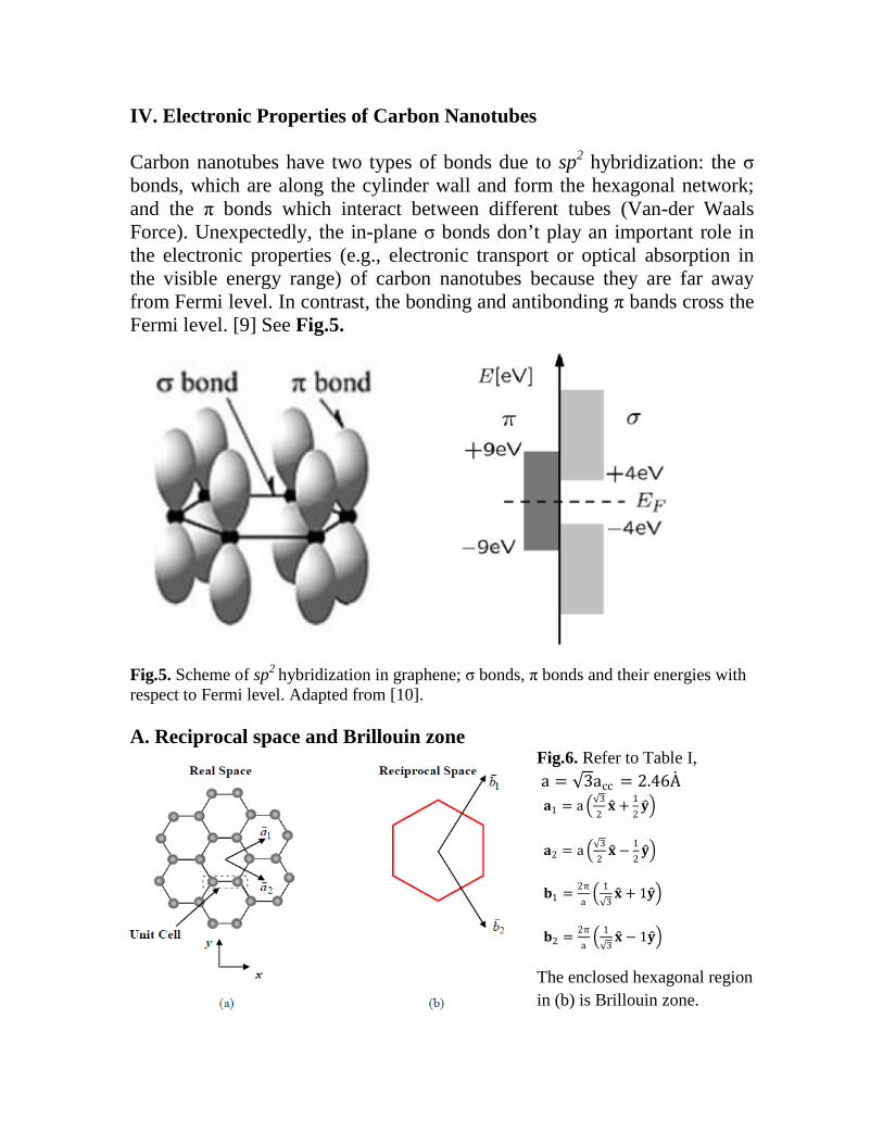
IV. Electronic Properties of Carbon Nanotubes Carbon nanotubes have two types of bonds due to sp2 hybridization: the σ bonds, which are along the cylinder wall and form the hexagonal network; and the π bonds which interact between different tubes (Van-der Waals Force). Unexpectedly, the in-plane σ bonds don’t play an important role in the electronic properties (e.g., electronic transport or optical absorption in the visible energy range) of carbon nanotubes because they are far away from Fermi level. In contrast, the bonding and antibonding π bands cross the Fermi level. [9] See Fig.5.
Fig.5. Scheme of sp2 hybridization in graphene; σ bonds, π bonds and their energies with respect to Fermi level. Adapted from [10]. A. Reciprocal space and Brillouin zone
Fig.6. Refer to Table I, a = √3acc = 2.46A 𝐚𝐚1 = a �√3
2𝐱𝐱� + 1
2𝐲𝐲��
𝐚𝐚2 = a �√32𝐱𝐱� − 1
2𝐲𝐲��
𝐛𝐛1 = 2πa� 1√3𝐱𝐱� + 1𝐲𝐲��
𝐛𝐛2 = 2πa� 1√3𝐱𝐱� − 1𝐲𝐲��
The enclosed hexagonal region in (b) is Brillouin zone.

B. Tight-binding model and band structure
In analogy with graphene, for given carbon atom, there are three nearest neighbors, as highlighted in Fig.7. For a single, flat graphene sheet, symmetry forbids coupling of π bands to σ bands that are well below and well above the Fermi energy. The π bands are well represented as linear combinations of pz orbitals of the carbon atoms, where z is perpendicular to the plane. Two bands of pz states will emerge due to the fact that graphene has two atoms per cell.
Fig.7. Consider area near the red ball as two-dimensional plane. If we define the coordinates of the red ball as (0, 0), then the three nearest neighbors are (0,− a
√3),
(− a2
, a2√3
), (a2
, a2√3
), respectively.
Continue with the assumption of linear combination of atomic orbitals (LCAO), we could follow Kittel’s textbook [11] and write:
ψk(𝐫𝐫) = ∑ Ckjφ(𝐫𝐫 − 𝐫𝐫𝐣𝐣)j (1)
In which φ(r) is the wave function for free electron moving in the electric
field of isolated atom. To construct Bloch functions, let Ckj = ei𝐤𝐤∙𝐫𝐫𝐣𝐣
√N, N is
normalized number (number of atoms in the system). Thus,
ψk(𝐫𝐫) = N−1/2 ∑ e(i𝐤𝐤∙𝐫𝐫𝐣𝐣)φ(𝐫𝐫−𝐫𝐫𝐣𝐣)j (2)
To calculate modified energy,

⟨𝐤𝐤|H|𝐤𝐤⟩ = N−1 ∑ ei𝐤𝐤∙(𝐫𝐫𝐣𝐣−𝐫𝐫𝐦𝐦)j,m �φm �H�φj� (3)
In which φm = φ(𝐫𝐫 − 𝐫𝐫𝐦𝐦)
Let 𝛒𝛒𝐦𝐦 = 𝐫𝐫𝐦𝐦 − 𝐫𝐫𝐣𝐣
⟨𝐤𝐤|H|𝐤𝐤⟩ = ∑ e(−i𝐤𝐤∙𝛒𝛒𝐦𝐦) ∫dVφ∗(𝐫𝐫 − 𝛒𝛒𝐦𝐦)m Hφ(𝐫𝐫) (4)
= γ0 � e(−i𝐤𝐤∙𝛒𝛒𝐦𝐦), in the case �𝐤𝐤�H(0)�𝐤𝐤�m
= 0,
γ0 = � dVφ∗(𝐫𝐫 − 𝛒𝛒𝐦𝐦) Hφ(𝐫𝐫) for nearest neighbor
Plug (0,− a√3
), (− a2
, a2√3
), (a2
, a2√3
) into the expression yields
H12(𝐤𝐤) = γ0[eik y a√3 + e
ik x a2 −
ik y a2√3 + e−
ik x a2 −
ik y a2√3 ], (5)
H12 (k) is specified in the in-secular equation
�H�(𝐤𝐤) − ε(𝐤𝐤)� = �−ε(𝐤𝐤) H12 (𝐤𝐤)
H12∗ (𝐤𝐤) −ε(𝐤𝐤) � = 0
Eventually we get
ε(𝐤𝐤) = ±|H12 (𝐤𝐤)| = ±γ0[1 + 4 cos �ky√3a
2� cos(kx
a2) + 4cos2((kx
a2)]1/2
(6)
Fig.8
Left: Band structure and first Brillouin zone from wikipedia.
Right: Reproduced with Mathematica, γ0 and a in arbitrary units.
C. Zone-folding approximation and metallicity
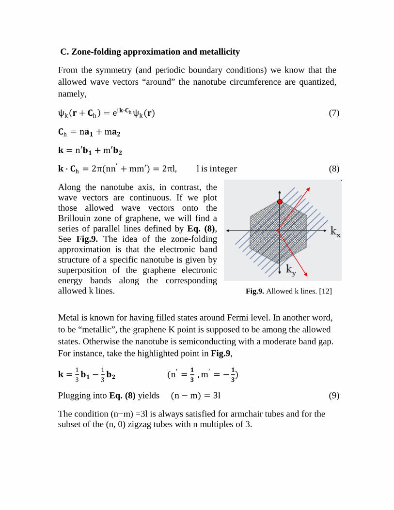
From the symmetry (and periodic boundary conditions) we know that the allowed wave vectors “around” the nanotube circumference are quantized, namely,
ψk(𝐫𝐫 + 𝐂𝐂h ) = ei𝐤𝐤∙𝐂𝐂hψk(𝐫𝐫) (7)
𝐂𝐂h = n𝐚𝐚𝟏𝟏 + m𝐚𝐚𝟐𝟐
𝐤𝐤 = n′𝐛𝐛𝟏𝟏 + m′𝐛𝐛𝟐𝟐
𝐤𝐤 ∙ 𝐂𝐂h = 2π(nn′ + mm′) = 2πl, l is integer (8)
Along the nanotube axis, in contrast, the wave vectors are continuous. If we plot those allowed wave vectors onto the Brillouin zone of graphene, we will find a series of parallel lines defined by Eq. (8), See Fig.9. The idea of the zone-folding approximation is that the electronic band structure of a specific nanotube is given by superposition of the graphene electronic energy bands along the corresponding allowed k lines. Fig.9. Allowed k lines. [12]
Metal is known for having filled states around Fermi level. In another word, to be “metallic”, the graphene K point is supposed to be among the allowed states. Otherwise the nanotube is semiconducting with a moderate band gap. For instance, take the highlighted point in Fig.9,
𝐤𝐤 = 13𝐛𝐛𝟏𝟏 −
13𝐛𝐛𝟐𝟐 (n′ = 𝟏𝟏
𝟑𝟑 , m′ = −𝟏𝟏
𝟑𝟑)
Plugging into Eq. (8) yields (n − m) = 3l (9)
The condition (n−m) =3l is always satisfied for armchair tubes and for the subset of the (n, 0) zigzag tubes with n multiples of 3.

D. Density of states (DOS) and Van Hove singularities
The density of states ∆N∆E
represents the number of available states for given energy interval. In this paragraph, theoretical calculation has been avoided, only experimental measurement and related physical concepts are sketched. The shape of the DOS depends on dimensionality, as shown below. These “spikes” in the DOS of 1D system are called Van Hove singularities and originate from the confinement properties in directions perpendicular to the tube axis.
Fig.10:
Left Top: Classifications of Carbon nanomaterials
Left Bottom: DOS for different dimensionalities [13]
Right Top: Van Hove singularities due to confinement of 1D electronic state on cutting lines [13] Right Bottom: Experimental spectra (solid line) compared with calculated data (dashed line). [14]
With Scanning Tunneling Spectroscopy (STS), people could really measure DOS. [15]

� dIdU�
U=V≈ ρsample (EF + eV)ρTip (EF) (10)
It’s interesting to notice those “spikes” in the DOS of 1D nanomaterial caused by the so called “Van Hove singularities”. Consider the energy and eigenstate of an ideal nanotube which is confined along x and y axes (~nm) but infinite along z axis:
ε = εi,j + ħ𝟐𝟐kz2
2m; ψ(x, y, z) = ψi,j(x, y)eikz (11)
In analogy with a rectangle, the solution for εi,j and ψi,j(x, y) are similar to the 2D”particle in a box” problem. [11]
D(ε) = �Di,j(ε)i,j
Di,j(ε) = ∑ dNi,j
dkdkdεi,j = ∑ 2 ∙ 2 ∙ L
2π[ m
2ħ2(ε−εi ,j )]1/2
i,j = �4L
hvi,j, ε > εi,j
0, ε < εi,j
� (12)
The first “2” comes from spin degeneracy; the second”2” is due to k has both positive and negative values; vi,j is the velocity of electron with kinetic energy(ε − εi,j). Near the “watershed” at εi,j , DOS will disperse due to the term(ε − εi,j)−1/2, this trait is called “Van Hove singularities”.
V. Other Physical Properties
Compared with other materials, carbon nanotubes have a series of extraordinary properties. (Fig 11) First of all, their sizes are small enough to be used in microscopic research. For instance, nanotube is already used to replace traditional tungsten tip because its shape is relatively stable. Second, its tensile strength extremely larger than high-strength steel alloys (45 billion pascals versus ~2 billion pascals). Third, its current carrying capacity is estimated to be 1billion amps per square centimeter (copper wires burn out at about 1 million amps per square centimeter). Besides, its heat transmission efficiency and temperature stability are both appreciably larger than traditional materials.

Fig.11. Other properties of Carbon nanotubes [5]

References:
[1]”There’s Plenty of Room at the Bottom” is the topic of a classic talk that Richard Feynman gave on December 29th 1959 at the annual meeting of the American Physical Society at the California Institute of Technology.
The transcript of the talk is available online: http://www.zyvex.com/nanotech/feynman.html
[2] Iijima, S., 1991, Nature (London) 354, 56.
[3] Iijima, S., and T. Ichihashi, 1993, Nature (London) 363, 603.
[4] Bethune, D. S., C. H. Kiang, M. S. de Vries, G. Gorman, R.Savoy, J.Vazquez, and R. Beyers, 1993, Nature (London) 363, 605.
[5] P. G. Collins and Ph. Avouris, Scientific American, 283, 62 (2000)
[6] Jean-Christophe Charlier, Blase, and Roche: Electronic and transport properties of nanotubes, Rev. Mod. Phys., Vol. 79, No. 2, April–June (2007)
[7] M.Damnjanović et al., “Full symmetry, optical activity, and potentials of single-wall and multiwall nanotubes”, Phys.Rev.B 60, 2728 (1999)
[8] Reich, S., C. Thomsen, and J. Maultzsch, 2004, Carbon Nanotubes, Basic Concepts and Physical Properties (Wiley-VCH Verlag GmbH, Weinheim).
[9] Charlier, J.-C., X. Gonze, and J.-P. Michenaud, 1991, Phys.Rev. B 43, 4579.
[10] Loiseau, A., P. Launois, P. Petit, S. Roche, and J.-P. Salvetat, 2006, Understanding Carbon Nanotubes From Basics to Applications, Lecture Notes in Physics Vol. 677 (Springer-Verlag, Berlin).
[11]Charles Kittel, 2005, Introduction to Solid State Physics, 8th ed. (John Wiley & Sons, New York)
[12] Mintmire, J. W., and C. T. White, 1998, Phys. Rev. Lett. 81, 2506.
[13]Gene Dresselhaus, 2008, The Novel Nanostructures of Carbon (Condensed Matter Symposium, Purdue University)
[14] Pavel V. Avramov ,1, Konstantin N. Kudin, Gustavo E. Scuseria, 2003, Chemical Physics Letters 370, 597
[15] Julian Chen, 2008, Introduction to Scanning Tunneling Microscopy (Oxford Science Publication)


![[R. Saito] Physical Properties of Carbon Nanotubes(BookFi.org)](https://static.fdocuments.in/doc/165x107/54e675c24a795943458b4b3a/r-saito-physical-properties-of-carbon-nanotubesbookfiorg.jpg)