PHYS225 Lecture 5people.physics.tamu.edu/depoy/phys225/Notes/lecture5.pdf · What is a Transistor?...
31
PHYS225 Lecture 5 Electronic Circuits
Transcript of PHYS225 Lecture 5people.physics.tamu.edu/depoy/phys225/Notes/lecture5.pdf · What is a Transistor?...

PHYS225Lecture 5
Electronic Circuits

Last lecture• Transfer Functions
– Behavior of a circuit for any possible input signal
• Can use “phasors” to describe any sinusoidal signal– In the complex plane– Can determine the phase and amplitude changes conveniently
• Leads to the idea of “complex impedance” or Z– Sort of the way resistance changes with frequency
• Z defines the influence of a component on the amplitude and phase of a circuit– Resistors: ZR = R
• change the amplitude by R
– Capacitors: ZC=1/jwC• change the amplitude by 1/wC• shift the phase -90 (1/j=-j)
– Inductors: ZL=jwL• change the amplitude by wL• shift the phase +90 (j)
• Can create “filters” that limit the frequency response of a circuit– High pass, low pass, bandpass, etc.

Last lecture• Diodes
– Semiconductor devices
– Passive components since there is no change in power
• Non-linear response
– Not like resistors!
– Turn on at some specific potential and conduct freely
• Can be used to “rectify” oscillatory signals
– Smoothed out more by application of capacitor
– Use a voltage regulator instead!

Active Components
• Transistors– Bipolar
– Field Effect
• Integrated Circuits– Analog
• Op Amps
– Digital
– Interface
• COTS components

The transistor was probably the most important invention of the 20th Century, and the story behind the invention is one of clashing egos and top secret research.
First - BJTs
Reference:Bell Labs MuseumB. G. Streetman & S. Banerjee ‘Solid State Electronic Devices’, Prentice Hall 1999.
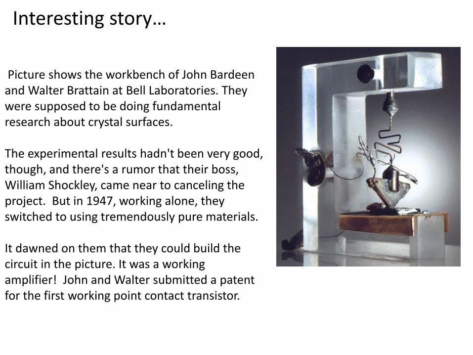
Picture shows the workbench of John Bardeen and Walter Brattain at Bell Laboratories. They were supposed to be doing fundamental research about crystal surfaces.
The experimental results hadn't been very good, though, and there's a rumor that their boss, William Shockley, came near to canceling the project. But in 1947, working alone, they switched to using tremendously pure materials.
It dawned on them that they could build the circuit in the picture. It was a working amplifier! John and Walter submitted a patent for the first working point contact transistor.
Interesting story…

Shockley was furious and took their work andinvented the junction transistor and submitted apatent for it 9 days later.
The three shared a Nobel Prize in 1955. Bardeenand Brattain continued in research (and Bardeenlater won another Nobel).
Shockley quit to start a semiconductor companyin Palo Alto. It folded, but its staff went on toinvent the integrated circuit (the "chip") and tofound Intel Corporation.
By 1960, all important computers usedtransistors for logic, and ferrite cores formemory.

Point-Contact Transistor – first transistor ever made


Qualitative basic operation of point-contact transistor
Problems with first transistor…

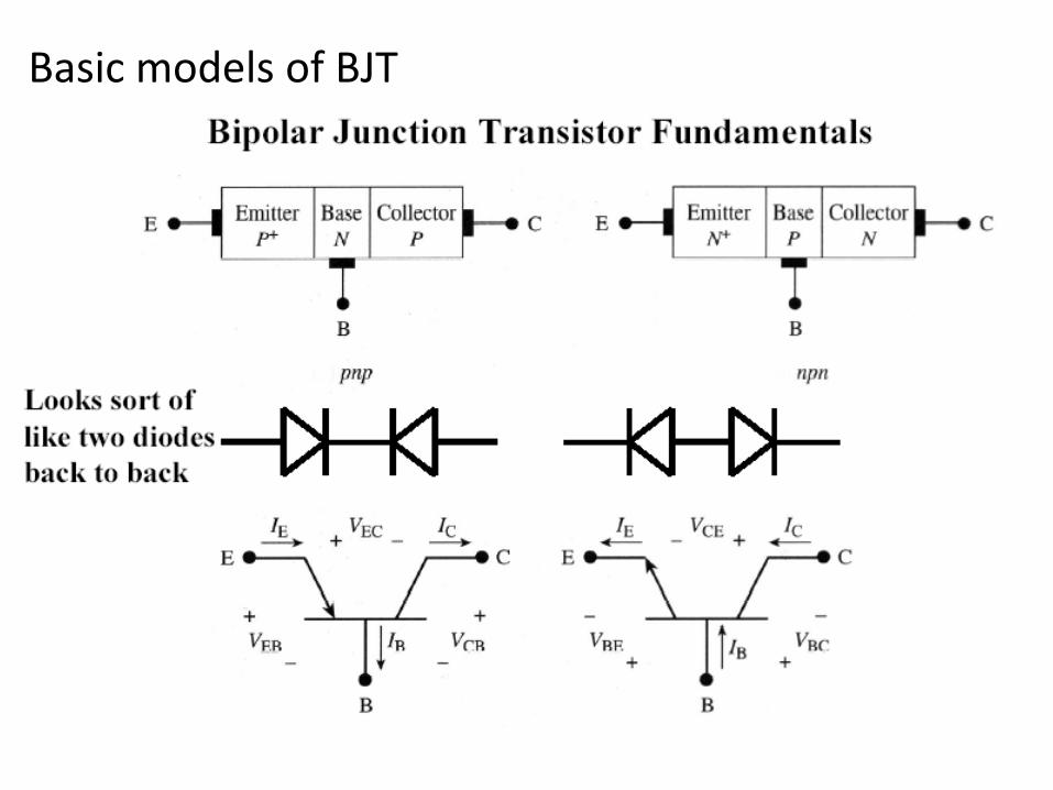
First Bipolar Junction Transistors
W. Shockley invented the p-n junction transistorThe physically relevant region is moved to the bulk of the material
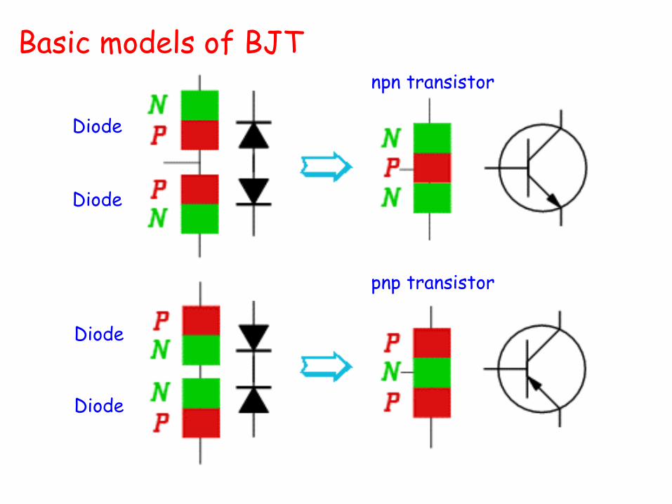
Basic models of BJT
Diode
Diode
Diode
Diode
npn transistor
pnp transistor

Qualitative basic operation of BJTs
Basic models of BJT

Background Science
• Conductors– Ex: Metals
– Flow of electricity governed by motion of free electrons
– As temperature increases, conductivity decreases due to more lattice atom collisions of electrons
– Idea of superconductivity
• Insulators– Ex: Plastics– Flow of electricity
governed by motion of ions that break free
– As temperature increases, conductivity increases due to lattice vibrations breaking free ions
– Irrelevant because conductive temperature beyond melting point

Semiconductors• Semiconductors are more like insulators in
their pure form but have smaller atomic band gaps
• Adding dopants allows them to gain conductive properties

Doping• Foreign elements are added to the semiconductor to make
it electropositive or electronegative
• P-type semiconductor (postive type)– Dopants include Boron, Aluminum, Gallium, Indium, and Thallium
– Ex: Silicon doped with Boron
– The boron atom will be involved in covalent bonds with three of the four neighboring Si atoms. The fourth bond will be missing and electron, giving the atom a “hole” that can accept an electron

Doping• N-type semiconductor (negative type)
– Dopants include Nitrogen, Phosphorous, Arsenic, Antimony, and Bismuth
• Ex: Silicon doped with Phosphorous– The Phosphorous atom will contribute and additional electron to
the Silicon giving it an excess negative charge
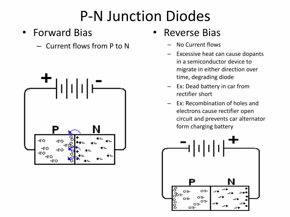
P-N Junction Diodes• Forward Bias
– Current flows from P to N
• Reverse Bias – No Current flows
– Excessive heat can cause dopants in a semiconductor device to migrate in either direction over time, degrading diode
– Ex: Dead battery in car from rectifier short
– Ex: Recombination of holes and electrons cause rectifier open circuit and prevents car alternator form charging battery

Back To The QuestionWhat is a Transistor?
• Bipolar Junction Transistors• NPN Transistor Most Common
Configuration• Base, Collector, and Emitter
– Base is a very thin region with less dopants
– Base collector junction reversed biased
– Base emitter junction forward biased
Fluid flow analogy:– If fluid flows into the base, a much
larger fluid can flow from the collector to the emitter
– If a signal to be amplified is applied as a current to the base, a valve between the collector and emitter opens and closes in response to signal fluctuations
• PNP Transistor essentially the same except for directionality

BJT Transistors
• BJT (Bipolar Junction Transistor)
– npn• Base is energized to allow current flow
– pnp• Base is connected to a lower potential to allow current flow
• 3 parameters of interest
– Current gain (β)
– Voltage drop from base to emitter when VBE=VFB
– Minimum voltage drop across the collector and emitter when transistor is saturated

BJT Relationships - Equations
B
CE
IE IC
IB
-
+
VBE VBC
+
-
+- VCE
B
CE
IE IC
IB-
+
VEB VCB
+
-
+ -VEC
npnIE = IB + IC
VCE = -VBC + VBE
pnpIE = IB + IC
VEC = VEB - VCB
Note: The equations seen above are for the transistor, not the circuit.

BJT ExampleUsing Common-Base NPN Circuit Configuration
+_
+_
Given: IB = 50 A , IC = 1 mAFind: IE , , and
Solution:
IE = IB + IC = 0.05 mA + 1 mA = 1.05 mA
= IC / IB = 1 mA / 0.05 mA = 20
= IC / IE = 1 mA / 1.05 mA = 0.95238
IC
IE
IB
VCB
VBE
E
C
B

BJT Transconductance CurveTypical NPN Transistor
VBE
IC
2 mA
4 mA
6 mA
8 mA
0.7 V
Collector Current:
IC = IES eVBE/VT
Transconductance: (slope of the curve)
gm = dIC /dVBE
IES = The reverse saturation current of the B-E Junction.
VT = kT/q = 26 mV (@ T=300K) = the emission coefficient and is
usually ~1

Eber-Moll BJT Model
The Eber-Moll Model for BJTs is fairly complex, but it is valid in all regions of BJT operation. The circuit diagram below shows all the components of the Eber-Moll Model:
E C
B
IRIF
IE IC
IB
RIERIC

Eber-Moll BJT Model
R = Common-base current gain (in forward active mode)F = Common-base current gain (in inverse active mode)IES = Reverse-Saturation Current of B-E JunctionICS = Reverse-Saturation Current of B-C Junction
IC = FIF – IR IB = IE - IC
IE = IF - RIR
IF = IES [exp(qVBE/kT) – 1] IR = IC [exp(qVBC/kT) – 1]
If IES & ICS are not given, they can be determined using various
BJT parameters.

Small Signal BJT Equivalent CircuitThe small-signal model can be used when the BJT is in the active region. The small-signal active-region model for a CB circuit is shown below:
iBr
iE
iCiB
B C
E
r = ( + 1) * VTIE
@ = 1 and T = 25C
r = ( + 1) * 0.026IE
= IC / IB

npn BJT Transistors
• High potential at collector
• Low potential at emitter
• Allows current flow when the base is given a high potential

pnp BJT Transistors
• High potential at emitter
• Low potential at collector
• Allows current flow when base is connected to a low potential

BJT Modes
• Cut-off Region: VBE < VFB, iB=0
– Transistor acts like an off switch
• Active Linear Region: VBE=VFB, iB≠0, iC=βiB– Transistor acts like a current amplifier
• Saturation Region: VBE=VFB, iB>iC,max/ β
– In this mode the transistor acts like an on switch
• Power across BJT

Power Across BJT
• PBJT = VCE * iCE
• Should be below the rated transistor power
• Should be kept in mind when considering heat dissipation
• Reducing power increases efficiency