
PHY Interface for the PCI Express Architecture - · PDF fileVersion 2.00 of the PCI Express...
38
PHY Interface for the PCI Express TM Architecture Version 2.00 ©2007 Intel Corporation—All rights reserved.
Transcript of PHY Interface for the PCI Express Architecture - · PDF fileVersion 2.00 of the PCI Express...
PHY Interface for the
PCI ExpressTM
Architecture
Version 2.00
©2007 Intel Corporation—All rights reserved.
PHY Interface for the PCI ExpressTM Architecture
©2007 Intel Corporation—All rights reserved. Page 2 of 38
Intellectual Property Disclaimer THIS SPECIFICATION IS PROVIDED “AS IS” WITH NO WARRANTIES WHATSOEVER INCLUDING ANY WARRANTY OF MERCHANTABILITY, FITNESS FOR ANY PARTICULAR PURPOSE, OR ANY WARRANTY OTHERWISE ARISING OUT OF ANY PROPOSAL, SPECIFICATION, OR SAMPLE. A COPYRIGHT LICENSE IS HEREBY GRANTED TO REPRODUCE AND DISTRIBUTE THIS SPECIFICATION FOR INTERNAL USE ONLY. NO OTHER LICENSE, EXPRESS OR IMPLIED, BY ESTOPPEL OR OTHERWISE, TO ANY OTHER INTELLECTUAL PROPERTY RIGHTS IS GRANTED OR INTENDED HEREBY. INTEL CORPORATION AND THE AUTHORS OF THIS SPECIFICATION DISCLAIM ALL LIABILITY, INCLUDING LIABILITY FOR INFRINGEMENT OF PROPRIETARY RIGHTS, RELATING TO IMPLEMENTATION OF INFORMATION IN THIS DOCUMENT AND THE SPECIFICATION. INTEL CORPORATION AND THE AUTHORS OF THIS SPECIFICATION ALSO DO NOT WARRANT OR REPRESENT THAT SUCH IMPLEMENTATION(S) WILL NOT INFRINGE SUCH RIGHTS. ALL SUGGESTIONS OR FEEDBACK RELATED TO THIS SPECIFICATION BECOME THE PROPERTY OF INTEL CORPORATION UPON SUBMISSION. INTEL CORPORATION MAY MAKE CHANGES TO SPECIFICATIONS, PRODUCT DESCRIPTIONS, AND PLANS AT ANY TIME, WITHOUT NOTICE. Notice: Implementations developed using the information provided in this specification may infringe the patent rights of various parties including the parties involved in the development of this specification. No license, express or implied, by estoppel or otherwise, to any intellectual property rights (including without limitation rights under any party’s patents) are granted herein. This document is an intermediate draft for comment only and is subject to change without notice. Readers should not design products based on this document. All product names are trademarks, registered trademarks, or service marks of their respective owners Contributors Jeff Morris Jim Choate Andy Martwick Paul Mattos Brad Hosler Matthew Myers
PHY Interface for the PCI ExpressTM Architecture
©2007 Intel Corporation—All rights reserved. Page 3 of 38
Table of Contents 1 Preface...................................................................................................................................... 5
1.1 Scope of this Revision ...................................................................................................... 5 1.2 Revision History ............................................................................................................... 5
2 Introduction .............................................................................................................................. 6 2.1 PCI Express PHY Layer ................................................................................................... 7
3 PHY/MAC Interface ................................................................................................................ 7 4 PCI Express PHY Functionality............................................................................................... 9
4.1 Transmitter Block Diagram ............................................................................................ 10 4.2 Receiver Block Diagram................................................................................................. 11 4.3 Clocking.......................................................................................................................... 11
5 PIPE Interface Signal Descriptions ........................................................................................ 12 5.1 PHY/MAC Interface Signals .......................................................................................... 12 5.2 External Signals .............................................................................................................. 15
6 PIPE Operational Behavior .................................................................................................... 17 6.1 Clocking.......................................................................................................................... 17 6.2 Reset................................................................................................................................ 17 6.3 Power Management ........................................................................................................ 17 6.4 Receiver Detection.......................................................................................................... 19 6.5 Transmitting a beacon..................................................................................................... 22 6.6 Detecting a beacon.......................................................................................................... 22 6.7 Clock Tolerance Compensation ...................................................................................... 23 6.8 Error Detection................................................................................................................ 24
6.8.1 8B/10B Decode Errors............................................................................................. 24 6.8.2 Disparity Errors ....................................................................................................... 25 6.8.3 Elastic Buffer Errors ................................................................................................ 25
6.9 Loopback ........................................................................................................................ 26 6.10 Polarity Inversion ........................................................................................................ 28 6.11 Setting negative disparity ............................................................................................ 28 6.12 Implementation specific timing................................................................................... 29 6.13 Control Signal Decode table........................................................................................ 31 6.14 Recommended synchronous signal timings ................................................................ 32
7 Sample Operational Sequences .............................................................................................. 32 7.1 Active PM L0 to L0s and back to L0.............................................................................. 32 7.2 Active PM to L1 and back to L0..................................................................................... 33 7.3 Receivers and Electrical Idle .......................................................................................... 34
8 Multi-lane PIPE...................................................................................................................... 37
PHY Interface for the PCI ExpressTM Architecture
©2007 Intel Corporation—All rights reserved. Page 4 of 38
Table of Figures Figure 1: Partitioning PHY Layer ........................................................................................................ 6 Figure 2: PHY/MAC Interface............................................................................................................. 7 Figure 3: PHY Functional Block Diagram ............................................................................................ 9 Figure 4: Transmitter Block Diagram ........................................................................................... 10 Figure 5: Receiver Block Diagram................................................................................................ 11 Figure 6: Clocking and Power Block Diagram ............................................................................. 11 Table of Tables Table 5-1: Transmit Data Interface Signals................................................................................... 12 Table 5-2: Receive Data Interface Signals .................................................................................... 12 Table 5-3: Command Interface Signals ......................................................................................... 13 Table 5-4: Status Interface Signals................................................................................................ 13 Table 5-5: External Signals ........................................................................................................... 15
PHY Interface for the PCI ExpressTM Architecture
©2007 Intel Corporation—All rights reserved. Page 5 of 38
1 Preface
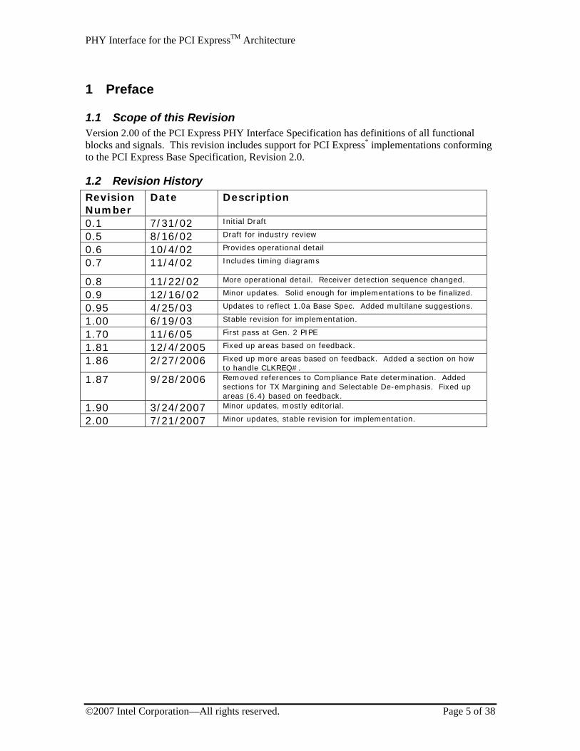
1.1 Scope of this Revision Version 2.00 of the PCI Express PHY Interface Specification has definitions of all functional blocks and signals. This revision includes support for PCI Express* implementations conforming to the PCI Express Base Specification, Revision 2.0.
1.2 Revision History Revision Number
Date Description
0.1 7/31/02 Initial Draft
0.5 8/16/02 Draft for industry review
0.6 10/4/02 Provides operational detail
0.7 11/4/02 Includes timing diagrams
0.8 11/22/02 More operational detail. Receiver detection sequence changed.
0.9 12/16/02 Minor updates. Solid enough for implementations to be finalized.
0.95 4/25/03 Updates to reflect 1.0a Base Spec. Added multilane suggestions.
1.00 6/19/03 Stable revision for implementation.
1.70 11/6/05 First pass at Gen. 2 PIPE
1.81 12/4/2005 Fixed up areas based on feedback.
1.86 2/27/2006 Fixed up more areas based on feedback. Added a section on how to handle CLKREQ#.
1.87 9/28/2006 Removed references to Compliance Rate determination. Added sections for TX Margining and Selectable De-emphasis. Fixed up areas (6.4) based on feedback.
1.90 3/24/2007 Minor updates, mostly editorial.
2.00 7/21/2007 Minor updates, stable revision for implementation.
PHY Interface for the PCI ExpressTM Architecture
©2007 Intel Corporation—All rights reserved. Page 6 of 38
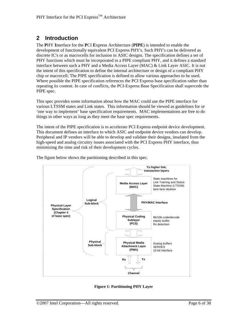
2 Introduction The PHY Interface for the PCI Express Architecture (PIPE) is intended to enable the development of functionally equivalent PCI Express PHY's. Such PHY's can be delivered as discrete IC's or as macrocells for inclusion in ASIC designs. The specification defines a set of PHY functions which must be incorporated in a PIPE compliant PHY, and it defines a standard interface between such a PHY and a Media Access Layer (MAC) & Link Layer ASIC. It is not the intent of this specification to define the internal architecture or design of a compliant PHY chip or macrocell; The PIPE specification is defined to allow various approaches to be used. Where possible the PIPE specification references the PCI Express base specification rather than repeating its content. In case of conflicts, the PCI-Express Base Specification shall supercede the PIPE spec. This spec provides some information about how the MAC could use the PIPE interface for various LTSSM states and Link states. This information should be viewed as guidelines for or ‘one way to implement’ base specification requirements. MAC implementations are free to do things in other ways as long as they meet the base spec requirements. The intent of the PIPE specification is to accelerate PCI Express endpoint device development. This document defines an interface to which ASIC and endpoint device vendors can develop. Peripheral and IP vendors will be able to develop and validate their designs, insulated from the high-speed and analog circuitry issues associated with the PCI Express PHY interface, thus minimizing the time and risk of their development cycles. The figure below shows the partitioning described in this spec.
Physical LayerSpecification
(Chapter 4of base spec)
State machines forLink Training and StatusState Machine (LTSSM)lane-lane deskew
8b/10b code/decodeelastic bufferRx detection
Analog buffersSERDES10-bit interface
LogicalSub-block
PhysicalSub-block
PHY/MAC Interface
To higher link,transaction layers
Physical CodingSublayer
(PCS)
Physical MediaAttachment Layer
(PMA)
Media Access Layer(MAC)
TxRx
Channel
Figure 1: Partitioning PHY Layer
PHY Interface for the PCI ExpressTM Architecture
©2007 Intel Corporation—All rights reserved. Page 7 of 38
2.1 PCI Express PHY Layer The PCI Express PHY Layer handles the low level PCI Express protocol and signaling. This includes features such as; data serialization and deserialization, 8b/10b encoding, analog buffers, elastic buffers and receiver detection. The primary focus of this block is to shift the clock domain of the data from the PCI Express rate to one that is compatible with the general logic in the ASIC. Some key features of the PCI Express PHY are: • Standard PHY interface enables multiple IP sources for PCI Express Logical Layer and
provides a target interface for PCI Express PHY vendors. • Supports 2.5GT/s only or 2.5GT/s and 5.0 GT/s serial data transmission rate • Utilizes 8-bit or 16-bit parallel interface to transmit and receive PCI Express data • Allows integration of high speed components into a single functional block as seen by the
endpoint device designer • Data and clock recovery from serial stream on the PCI Express bus • Holding registers to stage transmit and receive data • Supports direct disparity control for use in transmitting compliance pattern(s) • 8b/10b encode/decode and error indication • Receiver detection • Beacon transmission and reception • Selectable Tx Margining, Tx De-emphasis and signal swing values
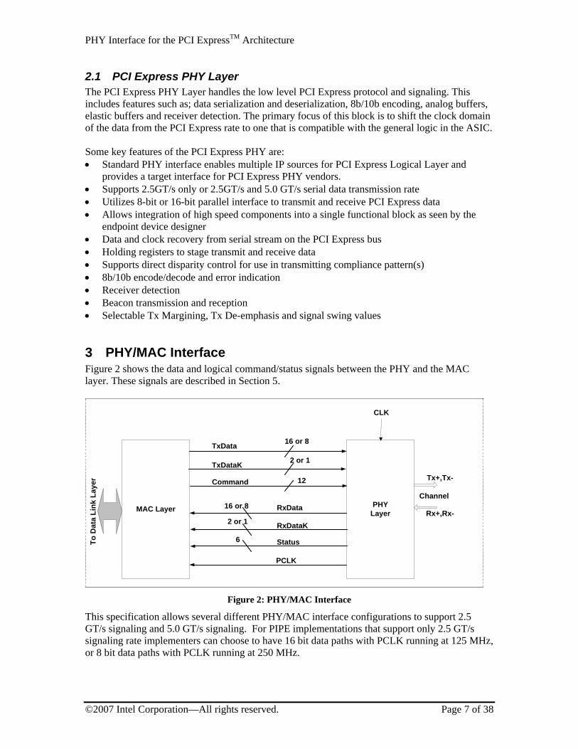
3 PHY/MAC Interface Figure 2 shows the data and logical command/status signals between the PHY and the MAC layer. These signals are described in Section 5.
MAC Layer PHYLayer
16 or 8
2 or 1
12
16 or 8
2 or 1
6
TxData
TxDataK
Command
RxData
RxDataK
StatusTo D
ata
Link
Lay
er Tx+,Tx-
Rx+,Rx-
Channel
CLK
PCLK
Figure 2: PHY/MAC Interface
This specification allows several different PHY/MAC interface configurations to support 2.5 GT/s signaling and 5.0 GT/s signaling. For PIPE implementations that support only 2.5 GT/s signaling rate implementers can choose to have 16 bit data paths with PCLK running at 125 MHz, or 8 bit data paths with PCLK running at 250 MHz.
PHY Interface for the PCI ExpressTM Architecture
©2007 Intel Corporation—All rights reserved. Page 8 of 38
PIPE implementations that support 5.0 GT/s signaling, and therefore are able to switch between 2.5 GT/s and 5.0 GT/s signaling rates, can be implemented in several ways. An implementation may choose to have PCLK fixed at 250 MHz and use 8-bit data paths when operating at 2.5 GT/s signaling rate, and 16-bit data paths when operating at 5.0 GT/s signaling rate. Another implementation choice is to use a fixed data path width and change PCLK frequency to adjust the signaling rate. In this case, an implementation with 8-bit data paths would provide PCLK at 250 MHz for 2.5 GT/s signaling and provide PCLK at 500 MHz for 5.0 GT/s signaling. Similarly, an implementation with 16-bit data paths would provide PCLK at 125 MHz for 2.5 GT/s signaling and 250 MHz for 5.0 GT/s signaling. While outside the scope of this specification, there may be PIPE implementations that support multiple of the above configurations. The mechanism for choosing the configuration to be used is implementation specific.
PHY Interface for the PCI ExpressTM Architecture
©2007 Intel Corporation—All rights reserved. Page 9 of 38
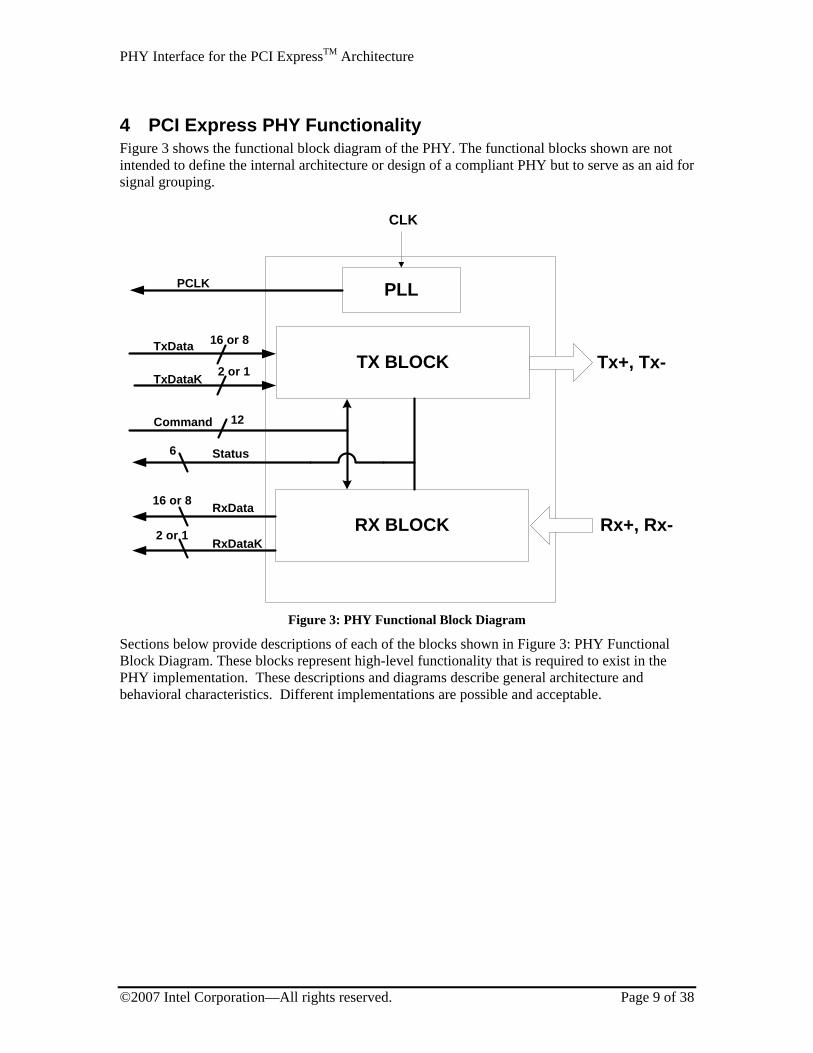
4 PCI Express PHY Functionality Figure 3 shows the functional block diagram of the PHY. The functional blocks shown are not intended to define the internal architecture or design of a compliant PHY but to serve as an aid for signal grouping.
TX BLOCK
RX BLOCK
PLL
12Command
16 or 8
2 or 1
TxData
TxDataK
Status
16 or 8
2 or 1
RxData
RxDataK
CLK
Tx+, Tx-
Rx+, Rx-
6
PCLK
Figure 3: PHY Functional Block Diagram
Sections below provide descriptions of each of the blocks shown in Figure 3: PHY Functional Block Diagram. These blocks represent high-level functionality that is required to exist in the PHY implementation. These descriptions and diagrams describe general architecture and behavioral characteristics. Different implementations are possible and acceptable.
PHY Interface for the PCI ExpressTM Architecture
©2007 Intel Corporation—All rights reserved. Page 10 of 38
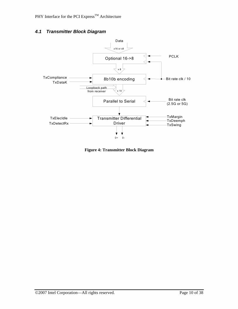
4.1 Transmitter Block Diagram
8b10b encoding
Parallel to Serial
Transmitter Differential Driver
D+ D-
Data
TxDataK
TxDetectRx
TxElecIdle
Bit rate clk / 10
Optional 16->8
Bit rate clk (2.5G or 5G)
x 8
x 10
x16 or x8
TxCompliance
PCLK
Loopback pathfrom receiver
TxMarginTxDeemphTxSwing
Figure 4: Transmitter Block Diagram
PHY Interface for the PCI ExpressTM Architecture
©2007 Intel Corporation—All rights reserved. Page 11 of 38
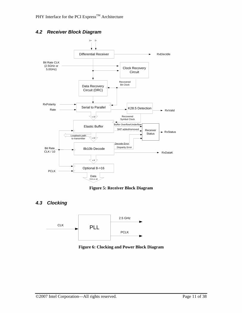
4.2 Receiver Block Diagram
Serial to Parallel
Differential Receiver
D+ D-
Clock Recovery Circuit
RxElecIdle
Recovered Bit Clock
K28.5 Detection
8b10b Decode
Recovered Symbol Clock
Elastic Buffer
RxPolarity
RxValid
RxDataK
Decode ErrorDisparity Error
Buffer Overflow/Underflow
SKP added/removed
Bit Rate CLK(2.5GHz or
5.0GHz)
Optional 8->16
Data
Data Recovery Circuit (DRC)
Bit Rate CLK / 10
PCLK
x 8
x 10
x 10
X16 or x8
ReceiverStatus RxStatus
Loopback pathto transmitter
Rate
Figure 5: Receiver Block Diagram
4.3 Clocking
PLL
2.5 GHz
CLK
PCLK
Figure 6: Clocking and Power Block Diagram
PHY Interface for the PCI ExpressTM Architecture
©2007 Intel Corporation—All rights reserved. Page 12 of 38
5 PIPE Interface Signal Descriptions
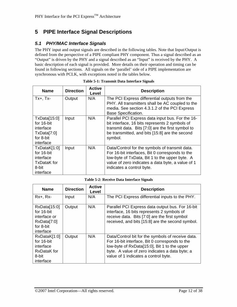
5.1 PHY/MAC Interface Signals The PHY input and output signals are described in the following tables. Note that Input/Output is defined from the perspective of a PIPE compliant PHY component. Thus a signal described as an “Output” is driven by the PHY and a signal described as an “Input” is received by the PHY. A basic description of each signal is provided. More details on their operation and timing can be found in following sections. All signals on the ‘parallel’ side of a PIPE implementation are synchronous with PCLK, with exceptions noted in the tables below.
Table 5-1: Transmit Data Interface Signals
Name Direction Active Level Description
Tx+, Tx- Output
N/A The PCI Express differential outputs from the PHY. All transmitters shall be AC coupled to the media. See section 4.3.1.2 of the PCI Express Base Specification.
TxData[15:0] for 16-bit interface TxData[7:0] for 8-bit interface
Input
N/A Parallel PCI Express data input bus. For the 16-bit interface, 16 bits represents 2 symbols of transmit data. Bits [7:0] are the first symbol to be transmitted, and bits [15:8] are the second symbol.
TxDataK[1:0]for 16-bit interface TxDataK for 8-bit interface
Input
N/A Data/Control for the symbols of transmit data. For 16-bit interfaces, Bit 0 corresponds to the low-byte of TxData, Bit 1 to the upper byte. A value of zero indicates a data byte, a value of 1 indicates a control byte.
Table 5-2: Receive Data Interface Signals
Name Direction Active Level Description
Rx+, Rx- Input
N/A The PCI Express differential inputs to the PHY.
RxData[15:0] for 16-bit interface or RxData[7:0] for 8-bit interface
Output
N/A Parallel PCI Express data output bus. For 16-bit interface, 16 bits represents 2 symbols of receive data. Bits [7:0] are the first symbol received, and bits [15:8] are the second symbol.
RxDataK[1:0] for 16-bit interface RxDataK for 8-bit interface
Output N/A Data/Control bit for the symbols of receive data. For 16-bit interface, Bit 0 corresponds to the low-byte of RxData[15:0], Bit 1 to the upper byte. A value of zero indicates a data byte; a value of 1 indicates a control byte.
PHY Interface for the PCI ExpressTM Architecture
©2007 Intel Corporation—All rights reserved. Page 13 of 38
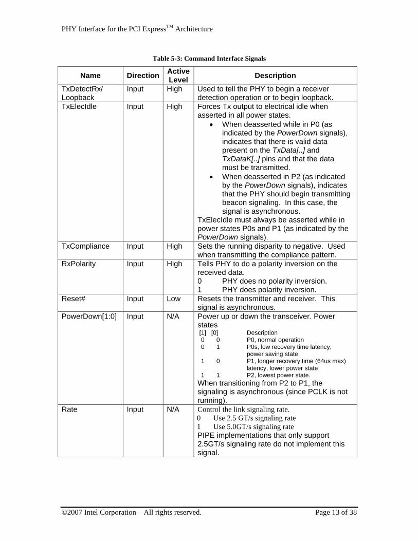
Table 5-3: Command Interface Signals
Name Direction Active Level Description
TxDetectRx/ Loopback
Input
High Used to tell the PHY to begin a receiver detection operation or to begin loopback.
TxElecIdle Input
High Forces Tx output to electrical idle when asserted in all power states.
• When deasserted while in P0 (as indicated by the PowerDown signals), indicates that there is valid data present on the TxData[..] and TxDataK[..] pins and that the data must be transmitted.
• When deasserted in P2 (as indicated by the PowerDown signals), indicates that the PHY should begin transmitting beacon signaling. In this case, the signal is asynchronous.
TxElecIdle must always be asserted while in power states P0s and P1 (as indicated by the PowerDown signals).
TxCompliance Input
High Sets the running disparity to negative. Used when transmitting the compliance pattern.
RxPolarity Input
High Tells PHY to do a polarity inversion on the received data. 0 PHY does no polarity inversion. 1 PHY does polarity inversion.
Reset# Input
Low Resets the transmitter and receiver. This signal is asynchronous.
PowerDown[1:0] Input
N/A Power up or down the transceiver. Power states [1] [0] Description 0 0 P0, normal operation 0 1 P0s, low recovery time latency, power saving state 1 0 P1, longer recovery time (64us max) latency, lower power state 1 1 P2, lowest power state. When transitioning from P2 to P1, the signaling is asynchronous (since PCLK is not running).
Rate Input N/A Control the link signaling rate. 0 Use 2.5 GT/s signaling rate 1 Use 5.0GT/s signaling rate PIPE implementations that only support 2.5GT/s signaling rate do not implement this signal.
PHY Interface for the PCI ExpressTM Architecture
©2007 Intel Corporation—All rights reserved. Page 14 of 38
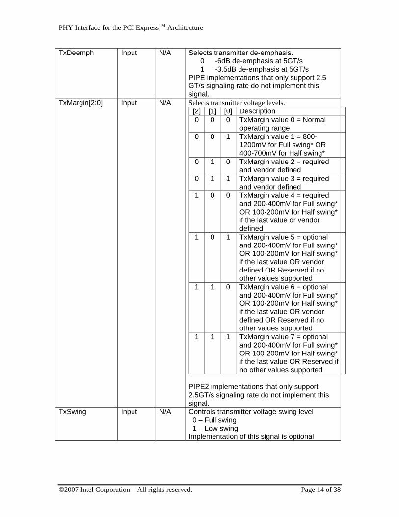
TxDeemph Input N/A Selects transmitter de-emphasis. 0 -6dB de-emphasis at 5GT/s 1 -3.5dB de-emphasis at 5GT/s
PIPE implementations that only support 2.5 GT/s signaling rate do not implement this signal.
TxMargin[2:0] Input N/A Selects transmitter voltage levels. [2] [1] [0] Description 0 0 0 TxMargin value 0 = Normal
operating range 0 0 1 TxMargin value 1 = 800-
1200mV for Full swing* OR 400-700mV for Half swing*
0 1 0 TxMargin value 2 = required and vendor defined
0 1 1 TxMargin value 3 = required and vendor defined
1 0 0 TxMargin value 4 = required and 200-400mV for Full swing* OR 100-200mV for Half swing* if the last value or vendor defined
1 0 1 TxMargin value 5 = optional and 200-400mV for Full swing* OR 100-200mV for Half swing* if the last value OR vendor defined OR Reserved if no other values supported
1 1 0 TxMargin value 6 = optional and 200-400mV for Full swing* OR 100-200mV for Half swing* if the last value OR vendor defined OR Reserved if no other values supported
1 1 1 TxMargin value 7 = optional and 200-400mV for Full swing* OR 100-200mV for Half swing* if the last value OR Reserved if no other values supported
PIPE2 implementations that only support 2.5GT/s signaling rate do not implement this signal.
TxSwing Input N/A Controls transmitter voltage swing level 0 – Full swing 1 – Low swing Implementation of this signal is optional
PHY Interface for the PCI ExpressTM Architecture
©2007 Intel Corporation—All rights reserved. Page 15 of 38
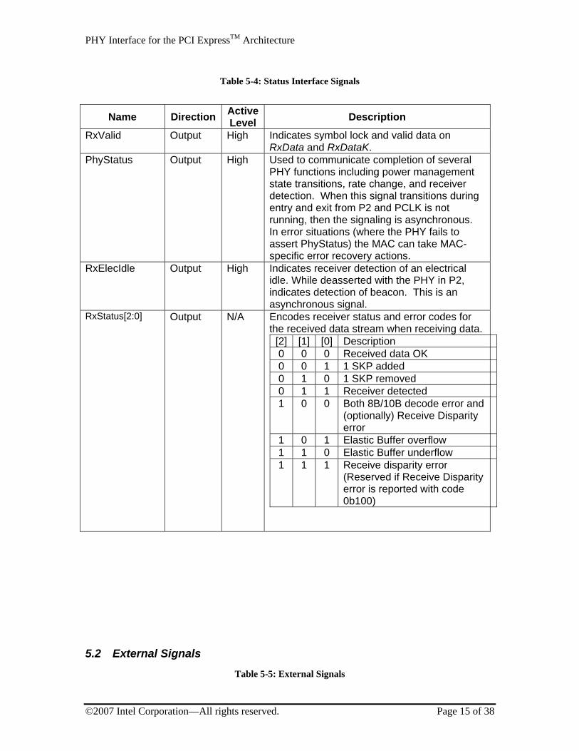
Table 5-4: Status Interface Signals
Name Direction Active Level Description
RxValid Output High Indicates symbol lock and valid data on RxData and RxDataK.
PhyStatus Output High Used to communicate completion of several PHY functions including power management state transitions, rate change, and receiver detection. When this signal transitions during entry and exit from P2 and PCLK is not running, then the signaling is asynchronous. In error situations (where the PHY fails to assert PhyStatus) the MAC can take MAC-specific error recovery actions.
RxElecIdle Output High Indicates receiver detection of an electrical idle. While deasserted with the PHY in P2, indicates detection of beacon. This is an asynchronous signal.
RxStatus[2:0] Output N/A Encodes receiver status and error codes for the received data stream when receiving data.
[2] [1] [0] Description 0 0 0 Received data OK 0 0 1 1 SKP added 0 1 0 1 SKP removed 0 1 1 Receiver detected 1 0 0 Both 8B/10B decode error and
(optionally) Receive Disparity error
1 0 1 Elastic Buffer overflow 1 1 0 Elastic Buffer underflow 1 1 1 Receive disparity error
(Reserved if Receive Disparity error is reported with code 0b100)
5.2 External Signals
Table 5-5: External Signals
PHY Interface for the PCI ExpressTM Architecture
©2007 Intel Corporation—All rights reserved. Page 16 of 38
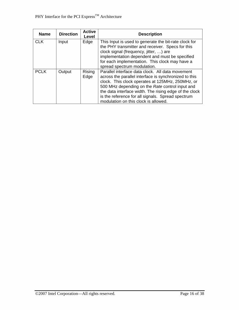
Name Direction Active Level Description
CLK Input Edge This Input is used to generate the bit-rate clock for the PHY transmitter and receiver. Specs for this clock signal (frequency, jitter, …) are implementation dependent and must be specified for each implementation. This clock may have a spread spectrum modulation.
PCLK Output Rising Edge
Parallel interface data clock. All data movement across the parallel interface is synchronized to this clock. This clock operates at 125MHz, 250MHz, or 500 MHz depending on the Rate control input and the data interface width. The rising edge of the clock is the reference for all signals. Spread spectrum modulation on this clock is allowed.
PHY Interface for the PCI ExpressTM Architecture
©2007 Intel Corporation—All rights reserved. Page 17 of 38
6 PIPE Operational Behavior
6.1 Clocking There are two clocks signals used by the PHY Interface component. The first (CLK) is a reference clock that the PHY uses to generate internal bit rate clocks for transmitting and receiving PCI Express data. The specifications for this signal are implementation dependent and must be fully specified by vendors. This clock may have spread spectrum modulation that matches a system reference clock (for example, the spread spectrum modulation could come from REFCLK from the Card Electro-Mechanical Specification). The second clock (PCLK) is an output from the PHY and is the parallel interface clock used to synchronize data transfers across the parallel interface. This clock runs at 125MHz, 250MHz, or 500 MHz depending on the Rate control input and data interface width. The rising edge of this clock is the reference point. This clock may also have spread spectrum modulation.
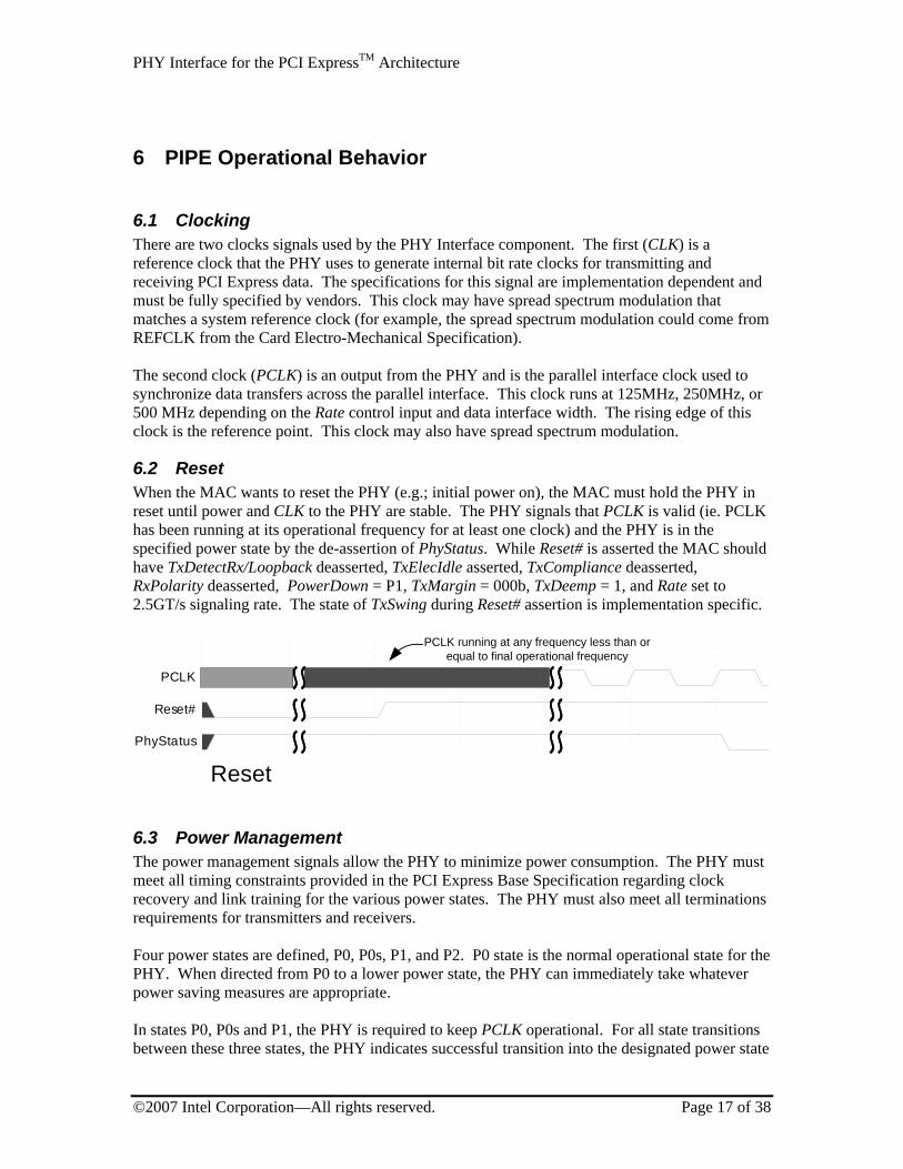
6.2 Reset When the MAC wants to reset the PHY (e.g.; initial power on), the MAC must hold the PHY in reset until power and CLK to the PHY are stable. The PHY signals that PCLK is valid (ie. PCLK has been running at its operational frequency for at least one clock) and the PHY is in the specified power state by the de-assertion of PhyStatus. While Reset# is asserted the MAC should have TxDetectRx/Loopback deasserted, TxElecIdle asserted, TxCompliance deasserted, RxPolarity deasserted, PowerDown = P1, TxMargin = 000b, TxDeemp = 1, and Rate set to 2.5GT/s signaling rate. The state of TxSwing during Reset# assertion is implementation specific.
PCLK running at any frequency less than orequal to final operational frequency
Reset
PCLK
Reset#
PhyStatus
6.3 Power Management The power management signals allow the PHY to minimize power consumption. The PHY must meet all timing constraints provided in the PCI Express Base Specification regarding clock recovery and link training for the various power states. The PHY must also meet all terminations requirements for transmitters and receivers. Four power states are defined, P0, P0s, P1, and P2. P0 state is the normal operational state for the PHY. When directed from P0 to a lower power state, the PHY can immediately take whatever power saving measures are appropriate. In states P0, P0s and P1, the PHY is required to keep PCLK operational. For all state transitions between these three states, the PHY indicates successful transition into the designated power state
PHY Interface for the PCI ExpressTM Architecture
©2007 Intel Corporation—All rights reserved. Page 18 of 38
by a single cycle assertion of PhyStatus. Transitions into and out of P2 are described below. For all power state transitions, the MAC must not begin any operational sequences or further power state transitions until the PHY has indicated that the initial state transition is completed. Mapping of PHY power states to states in the Link Training and Status State Machine (LTSSM) found in the base specification are included below. • P0 state: All internal clocks in the PHY are operational. P0 is the only state where the PHY
transmits and receives PCI Express signaling. P0 is the appropriate PHY power management state for most states in the Link Training and Status State Machine (LTSSM). Exceptions are listed below for each lower power PHY state.
• P0s state: PCLK output must stay operational. The MAC will move the PHY to this state only when the transmit channel is idle. P0s state can be used when the transmitter is in state Tx_L0s.Idle.
While the PHY is in either P0 or P0s power states, if the receiver is detecting an electrical idle, the receiver portion of the PHY can take appropriate power saving measures. Note that the PHY must be capable of obtaining bit and symbol lock within the PHY-specified time (N_FTS with/without common clock) upon resumption of signaling on the receive channel. This requirement only applies if the receiver had previously been bit and symbol locked while in P0 or P0s states.
• P1 state: Selected internal clocks in the PHY can be turned off. PCLK output must stay operational. The MAC will move the PHY to this state only when both transmit and receive channels are idle. The PHY must not indicate successful entry into P1 (by asserting PhyStatus) until PCLK is stable and the operating DC common mode voltage is stable and within specification (as per the base spec). P1 can be used for the Disabled state, all Detect states, and L1.Idle state of the Link Training and Status State Machine (LTSSM).
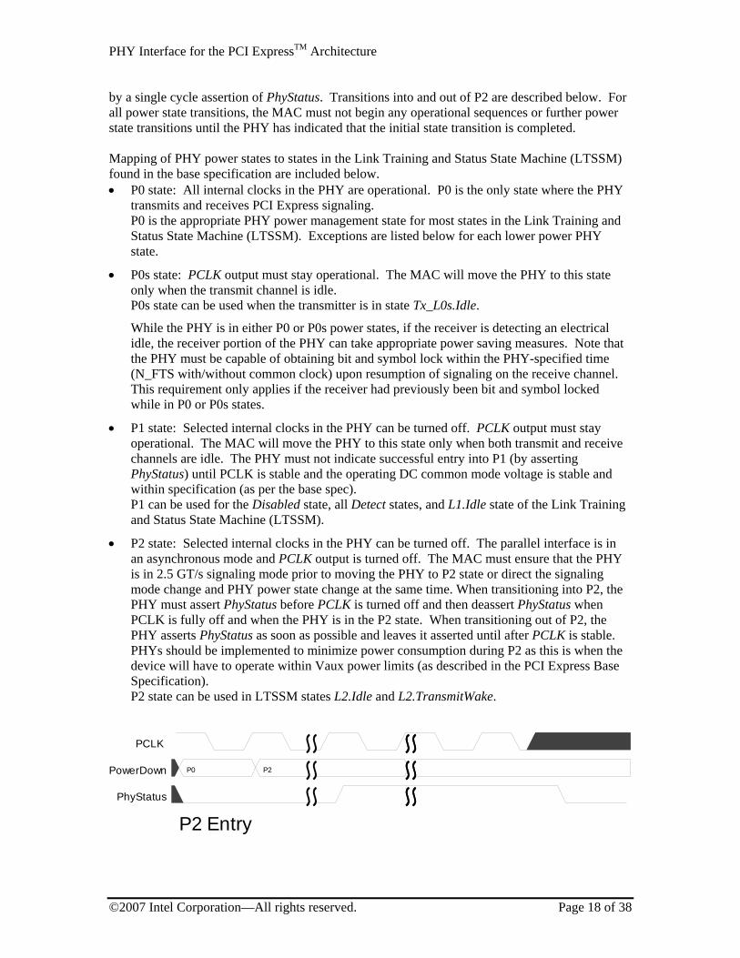
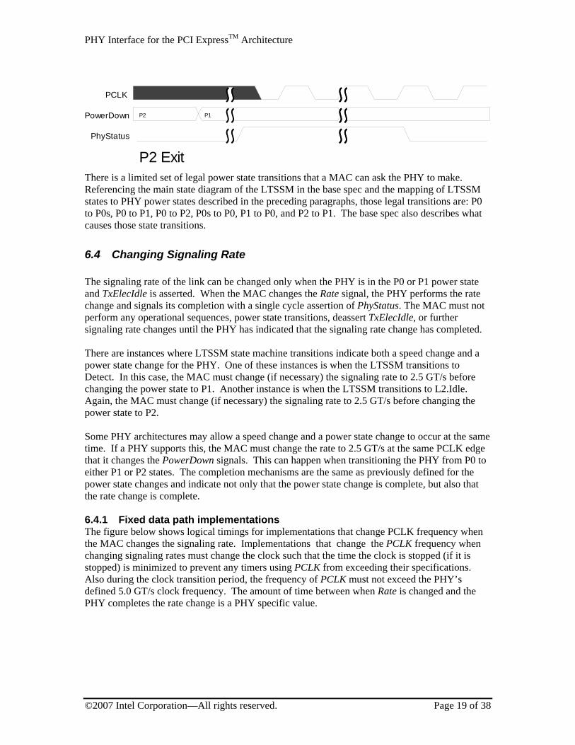
• P2 state: Selected internal clocks in the PHY can be turned off. The parallel interface is in an asynchronous mode and PCLK output is turned off. The MAC must ensure that the PHY is in 2.5 GT/s signaling mode prior to moving the PHY to P2 state or direct the signaling mode change and PHY power state change at the same time. When transitioning into P2, the PHY must assert PhyStatus before PCLK is turned off and then deassert PhyStatus when PCLK is fully off and when the PHY is in the P2 state. When transitioning out of P2, the PHY asserts PhyStatus as soon as possible and leaves it asserted until after PCLK is stable. PHYs should be implemented to minimize power consumption during P2 as this is when the device will have to operate within Vaux power limits (as described in the PCI Express Base Specification). P2 state can be used in LTSSM states L2.Idle and L2.TransmitWake.
P0 P2
P2 Entry
PCLK
PowerDown
PhyStatus
PHY Interface for the PCI ExpressTM Architecture
©2007 Intel Corporation—All rights reserved. Page 19 of 38
P2 P1
P2 Exit
PCLK
PowerDown
PhyStatus
There is a limited set of legal power state transitions that a MAC can ask the PHY to make. Referencing the main state diagram of the LTSSM in the base spec and the mapping of LTSSM states to PHY power states described in the preceding paragraphs, those legal transitions are: P0 to P0s, P0 to P1, P0 to P2, P0s to P0, P1 to P0, and P2 to P1. The base spec also describes what causes those state transitions.
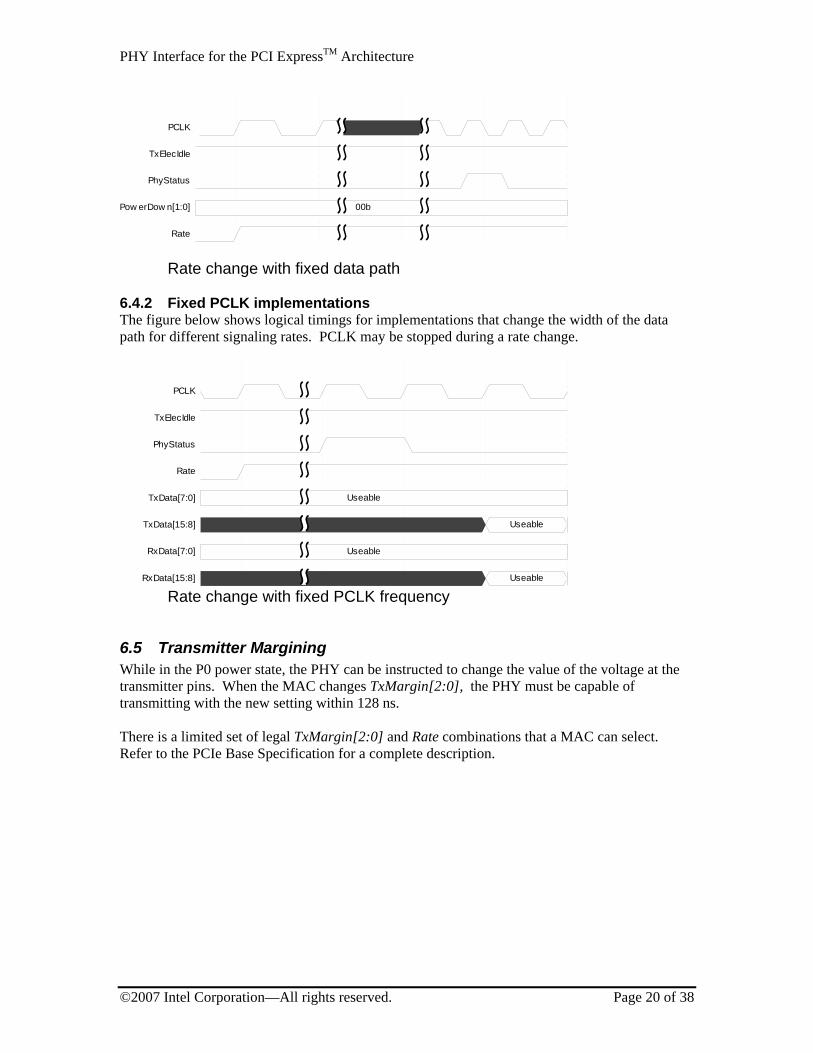
6.4 Changing Signaling Rate The signaling rate of the link can be changed only when the PHY is in the P0 or P1 power state and TxElecIdle is asserted. When the MAC changes the Rate signal, the PHY performs the rate change and signals its completion with a single cycle assertion of PhyStatus. The MAC must not perform any operational sequences, power state transitions, deassert TxElecIdle, or further signaling rate changes until the PHY has indicated that the signaling rate change has completed. There are instances where LTSSM state machine transitions indicate both a speed change and a power state change for the PHY. One of these instances is when the LTSSM transitions to Detect. In this case, the MAC must change (if necessary) the signaling rate to 2.5 GT/s before changing the power state to P1. Another instance is when the LTSSM transitions to L2.Idle. Again, the MAC must change (if necessary) the signaling rate to 2.5 GT/s before changing the power state to P2. Some PHY architectures may allow a speed change and a power state change to occur at the same time. If a PHY supports this, the MAC must change the rate to 2.5 GT/s at the same PCLK edge that it changes the PowerDown signals. This can happen when transitioning the PHY from P0 to either P1 or P2 states. The completion mechanisms are the same as previously defined for the power state changes and indicate not only that the power state change is complete, but also that the rate change is complete. 6.4.1 Fixed data path implementations The figure below shows logical timings for implementations that change PCLK frequency when the MAC changes the signaling rate. Implementations that change the PCLK frequency when changing signaling rates must change the clock such that the time the clock is stopped (if it is stopped) is minimized to prevent any timers using PCLK from exceeding their specifications. Also during the clock transition period, the frequency of PCLK must not exceed the PHY’s defined 5.0 GT/s clock frequency. The amount of time between when Rate is changed and the PHY completes the rate change is a PHY specific value.
PHY Interface for the PCI ExpressTM Architecture
©2007 Intel Corporation—All rights reserved. Page 20 of 38
00b
PCLK
TxElecIdle
PhyStatus
Pow erDow n[1:0]
Rate
Rate change with fixed data path
6.4.2 Fixed PCLK implementations The figure below shows logical timings for implementations that change the width of the data path for different signaling rates. PCLK may be stopped during a rate change.
Useable
Useable
Useable
Useable
PCLK
TxElecIdle
PhyStatus
Rate
TxData[7:0]
TxData[15:8]
RxData[7:0]
RxData[15:8] Rate change with fixed PCLK frequency
6.5 Transmitter Margining While in the P0 power state, the PHY can be instructed to change the value of the voltage at the transmitter pins. When the MAC changes TxMargin[2:0], the PHY must be capable of transmitting with the new setting within 128 ns. There is a limited set of legal TxMargin[2:0] and Rate combinations that a MAC can select. Refer to the PCIe Base Specification for a complete description.
PHY Interface for the PCI ExpressTM Architecture
©2007 Intel Corporation—All rights reserved. Page 21 of 38
PCLK
TxMargin[2:0]
Tx+/Tx-
New value atTx pins within 128ns
Selecting Tx Margining value
Current Tx Margin Value New Tx Margin Value
Current Tx Margin Value New Tx Margin Value
< 128ns
PowerDown[1:0] P0 P0
6.6 Selectable De-emphasis While in the P0 power state and transmitting at 5.0GT/s, the PHY can be instructed to change the value of the transmitter de-emphasis. When the MAC changes TxDeemph, the PHY must be capable of transmitting with the new setting within 128 ns. There is a limited set of legal TxDeemph and Rate combinations that a MAC can select. Refer to the PCIe Base Specification for a complete description. The MAC must ensure that TxDeemph is selecting -3.5db whenever Rate is selecting 2.5 GT/s.
PCLK
TxDeemph
Tx+/Tx-
New value atTx pins within 128ns
Selecting Tx De-emphasis value
Current Tx De-emphasis Value New Tx De-emphasis Value
Current Tx De=emphasis Value New Tx De-emphasis Value
< 128ns
PowerDown[1:0] P0 P0
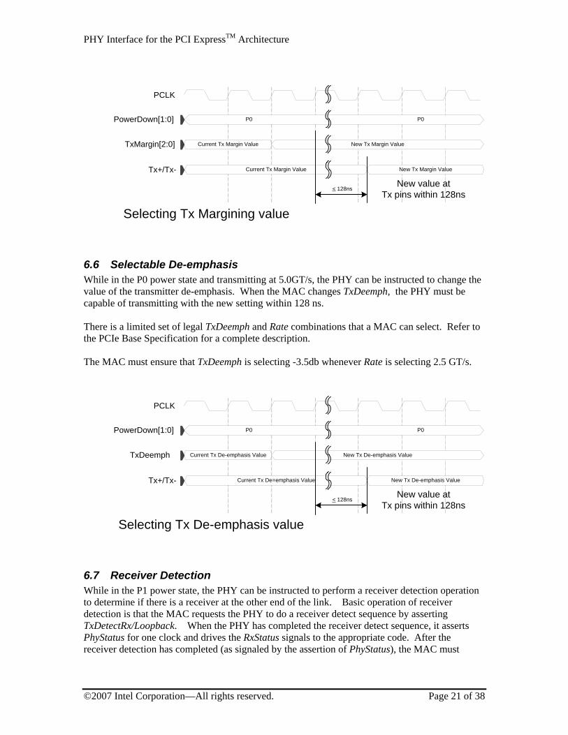
6.7 Receiver Detection While in the P1 power state, the PHY can be instructed to perform a receiver detection operation to determine if there is a receiver at the other end of the link. Basic operation of receiver detection is that the MAC requests the PHY to do a receiver detect sequence by asserting TxDetectRx/Loopback. When the PHY has completed the receiver detect sequence, it asserts PhyStatus for one clock and drives the RxStatus signals to the appropriate code. After the receiver detection has completed (as signaled by the assertion of PhyStatus), the MAC must
PHY Interface for the PCI ExpressTM Architecture
©2007 Intel Corporation—All rights reserved. Page 22 of 38
deassert TxDetectRx/Loopback before initiating another receiver detection, a power state transition, or signaling a rate change. Once the MAC has requested a receiver detect sequence (by asserting TxDetectRx/Loopback), the MAC must leave TxDetectRx/Loopback asserted until after the PHY has signaled completion by the assertion of PhyStatus.
Detected Condition RxStatus code Receiver not present 000b Receiver present 011b
10b
000b 011b 000b
Receiver Detect - Receiver present
PCLK
TxDetectRx/Loopback
PhyStatus
PowerDown[1:0]
RxStatus
6.8 Transmitting a beacon When the PHY has been put in the P2 power state, and the MAC wants to transmit a beacon, the MAC deasserts TxElecIdle and the PHY should generate a valid beacon until TxElecIdle is asserted. The MAC must assert TxElecIdle before transitioning the PHY to P0.
P2
Val id beacon signaling
Beacon Transmit
PowerDown[1:0]
TxElecIdle
Tx+/Tx-
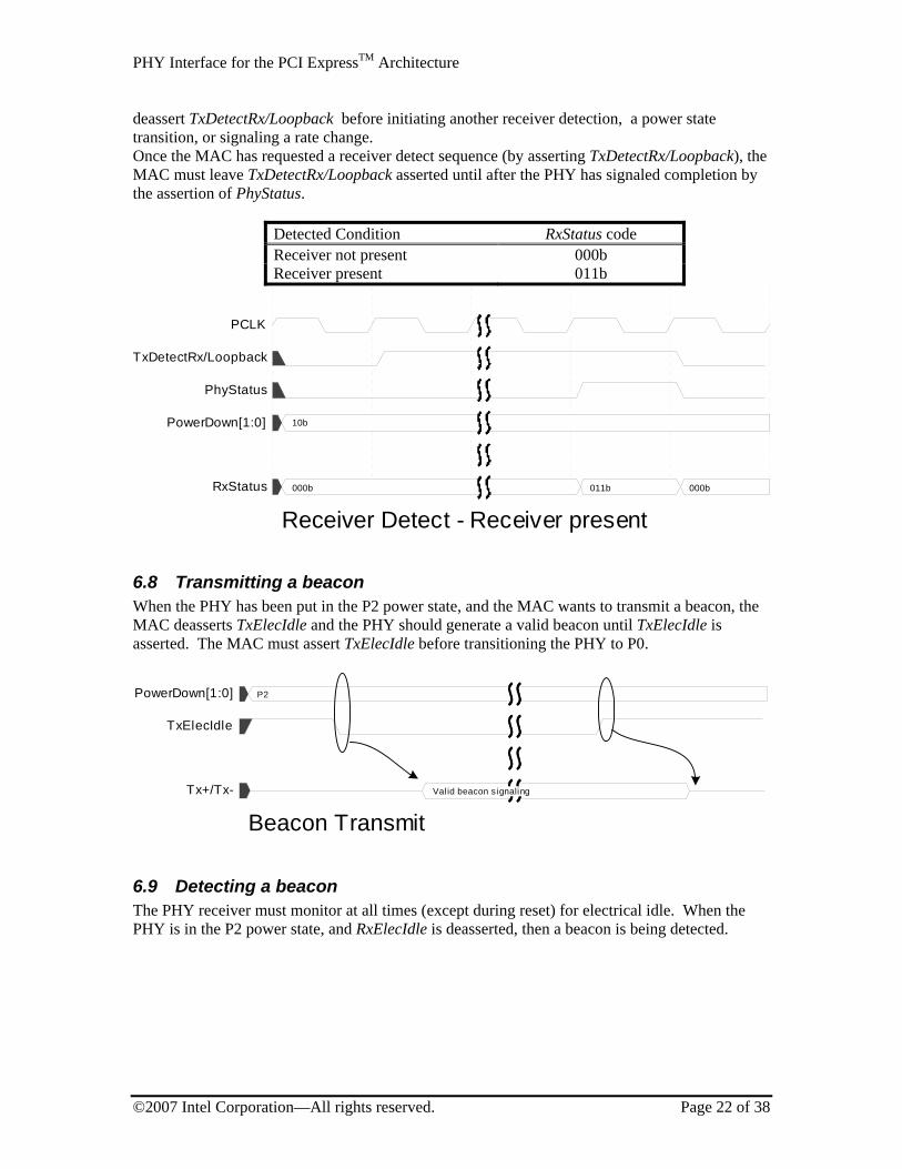
6.9 Detecting a beacon The PHY receiver must monitor at all times (except during reset) for electrical idle. When the PHY is in the P2 power state, and RxElecIdle is deasserted, then a beacon is being detected.
PHY Interface for the PCI ExpressTM Architecture
©2007 Intel Corporation—All rights reserved. Page 23 of 38
P2
Valid beacon signaling
Beacon Receive
PowerDown[1:0]
RxElecIdle
Rx+/Rx-
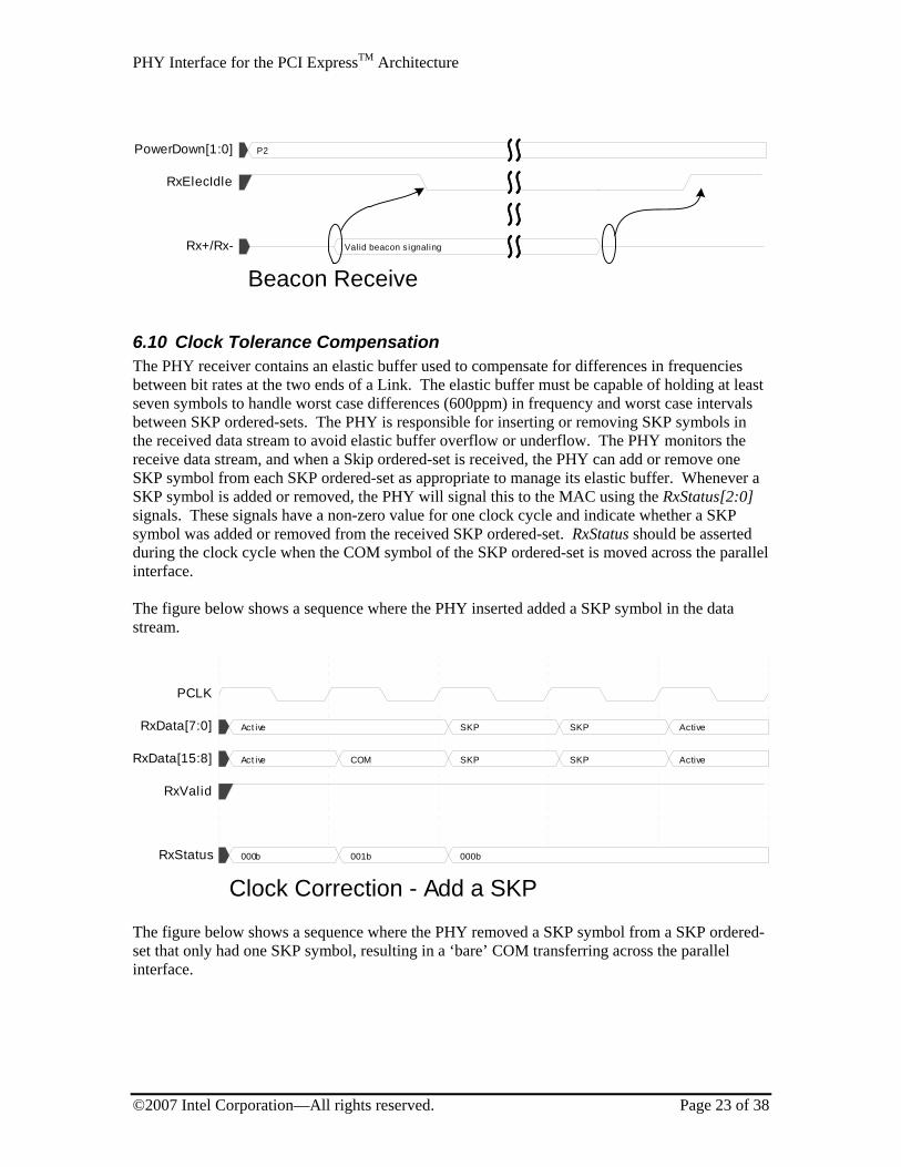
6.10 Clock Tolerance Compensation The PHY receiver contains an elastic buffer used to compensate for differences in frequencies between bit rates at the two ends of a Link. The elastic buffer must be capable of holding at least seven symbols to handle worst case differences (600ppm) in frequency and worst case intervals between SKP ordered-sets. The PHY is responsible for inserting or removing SKP symbols in the received data stream to avoid elastic buffer overflow or underflow. The PHY monitors the receive data stream, and when a Skip ordered-set is received, the PHY can add or remove one SKP symbol from each SKP ordered-set as appropriate to manage its elastic buffer. Whenever a SKP symbol is added or removed, the PHY will signal this to the MAC using the RxStatus[2:0] signals. These signals have a non-zero value for one clock cycle and indicate whether a SKP symbol was added or removed from the received SKP ordered-set. RxStatus should be asserted during the clock cycle when the COM symbol of the SKP ordered-set is moved across the parallel interface. The figure below shows a sequence where the PHY inserted added a SKP symbol in the data stream.
Act ive COM SKP SKP Active
Act ive SKP SKP Active
000b 001b 000b
Clock Correction - Add a SKP
PCLK
RxData[7:0]
RxData[15:8]
RxValid
RxStatus
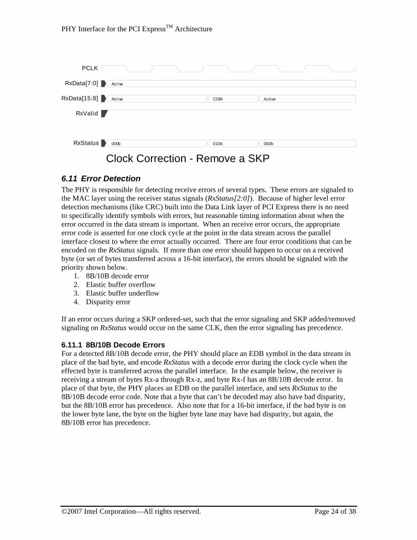
The figure below shows a sequence where the PHY removed a SKP symbol from a SKP ordered-set that only had one SKP symbol, resulting in a ‘bare’ COM transferring across the parallel interface.
PHY Interface for the PCI ExpressTM Architecture
©2007 Intel Corporation—All rights reserved. Page 24 of 38
Act ive COM Active
Act ive
000b 010b 000b
Clock Correction - Remove a SKP
PCLK
RxData[7:0]
RxData[15:8]
RxValid
RxStatus
6.11 Error Detection The PHY is responsible for detecting receive errors of several types. These errors are signaled to the MAC layer using the receiver status signals (RxStatus[2:0]). Because of higher level error detection mechanisms (like CRC) built into the Data Link layer of PCI Express there is no need to specifically identify symbols with errors, but reasonable timing information about when the error occurred in the data stream is important. When an receive error occurs, the appropriate error code is asserted for one clock cycle at the point in the data stream across the parallel interface closest to where the error actually occurred. There are four error conditions that can be encoded on the RxStatus signals. If more than one error should happen to occur on a received byte (or set of bytes transferred across a 16-bit interface), the errors should be signaled with the priority shown below.
1. 8B/10B decode error 2. Elastic buffer overflow 3. Elastic buffer underflow 4. Disparity error
If an error occurs during a SKP ordered-set, such that the error signaling and SKP added/removed signaling on RxStatus would occur on the same CLK, then the error signaling has precedence. 6.11.1 8B/10B Decode Errors For a detected 8B/10B decode error, the PHY should place an EDB symbol in the data stream in place of the bad byte, and encode RxStatus with a decode error during the clock cycle when the effected byte is transferred across the parallel interface. In the example below, the receiver is receiving a stream of bytes Rx-a through Rx-z, and byte Rx-f has an 8B/10B decode error. In place of that byte, the PHY places an EDB on the parallel interface, and sets RxStatus to the 8B/10B decode error code. Note that a byte that can’t be decoded may also have bad disparity, but the 8B/10B error has precedence. Also note that for a 16-bit interface, if the bad byte is on the lower byte lane, the byte on the higher byte lane may have bad disparity, but again, the 8B/10B error has precedence.
PHY Interface for the PCI ExpressTM Architecture
©2007 Intel Corporation—All rights reserved. Page 25 of 38
Rx-b Rx-d EDB Rx-I Rx-k
Rx-a Rx-c Rx-e Rx-h Rx-j
000b 100b 000b
8B/10B Decode Error
PCLK
RxData[7:0]
RxData[15:8]
RxValid
RxStatus
6.11.2 Disparity Errors For a detected disparity error, the PHY should assert RxStatus with the disparity error code during the clock cycle when the effected byte is transferred across the parallel interface. For 16-bit interfaces, it is not possible to discern which byte (or possibly both) had the disparity error. In the example below, the receiver detected a disparity error on either (or both) Rx-e or Rx-f data bytes, and indicates this with the assertion of RxStatus. Optionally, the PHY can signal disparity errors as 8B/10B decode error (using code 0b100). (MACs often treat 8B/10B errors and disparity errors identically.)
Rx-b Rx-d Rx-f Rx-I Rx-k
Rx-a Rx-c Rx-e Rx-h Rx-j
00b 111b 000b
Disparity Error
PCLK
RxData[7:0]
RxData[15:8]
RxValid
RxStatus
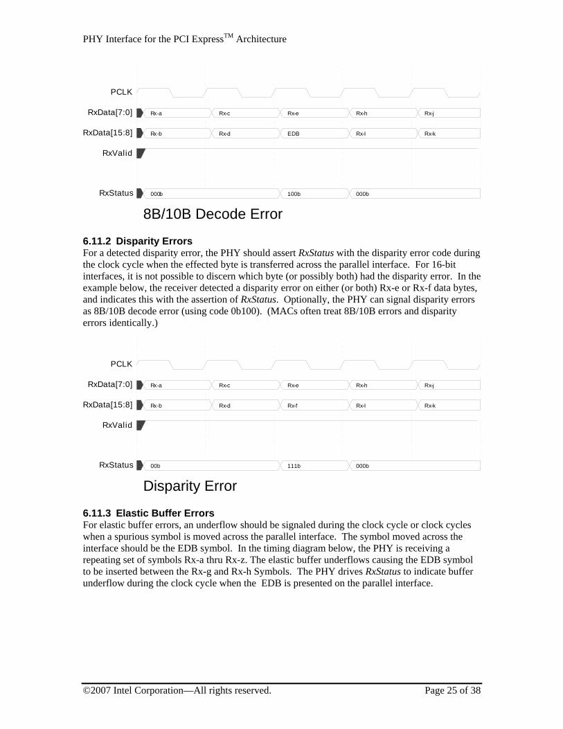
6.11.3 Elastic Buffer Errors For elastic buffer errors, an underflow should be signaled during the clock cycle or clock cycles when a spurious symbol is moved across the parallel interface. The symbol moved across the interface should be the EDB symbol. In the timing diagram below, the PHY is receiving a repeating set of symbols Rx-a thru Rx-z. The elastic buffer underflows causing the EDB symbol to be inserted between the Rx-g and Rx-h Symbols. The PHY drives RxStatus to indicate buffer underflow during the clock cycle when the EDB is presented on the parallel interface.
PHY Interface for the PCI ExpressTM Architecture
©2007 Intel Corporation—All rights reserved. Page 26 of 38
Rx-b Rx-d Rx-f EDB Rx-I
Rx-a Rx-c Rx-e Rx-g Rx-h
00b 110b 00b
Elastic Buffer Underflow
PCLK
RxData[7:0]
RxData[15:8]
RxValid
RxStatus
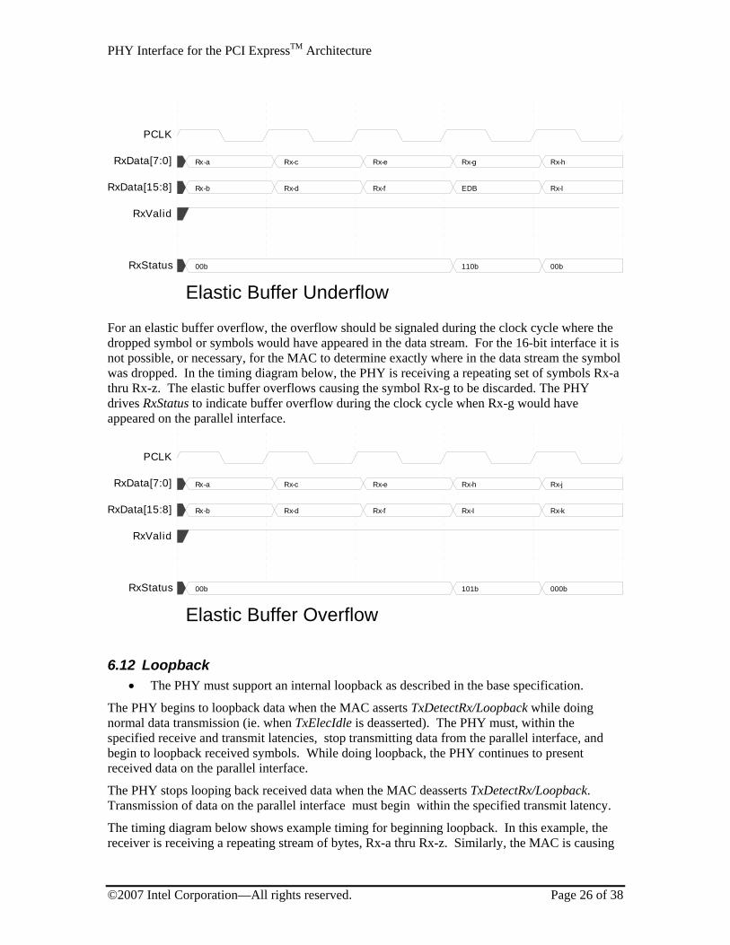
For an elastic buffer overflow, the overflow should be signaled during the clock cycle where the dropped symbol or symbols would have appeared in the data stream. For the 16-bit interface it is not possible, or necessary, for the MAC to determine exactly where in the data stream the symbol was dropped. In the timing diagram below, the PHY is receiving a repeating set of symbols Rx-a thru Rx-z. The elastic buffer overflows causing the symbol Rx-g to be discarded. The PHY drives RxStatus to indicate buffer overflow during the clock cycle when Rx-g would have appeared on the parallel interface.
Rx-b Rx-d Rx-f Rx-I Rx-k
Rx-a Rx-c Rx-e Rx-h Rx-j
00b 101b 000b
Elastic Buffer Overflow
PCLK
RxData[7:0]
RxData[15:8]
RxValid
RxStatus
6.12 Loopback • The PHY must support an internal loopback as described in the base specification.
The PHY begins to loopback data when the MAC asserts TxDetectRx/Loopback while doing normal data transmission (ie. when TxElecIdle is deasserted). The PHY must, within the specified receive and transmit latencies, stop transmitting data from the parallel interface, and begin to loopback received symbols. While doing loopback, the PHY continues to present received data on the parallel interface.
The PHY stops looping back received data when the MAC deasserts TxDetectRx/Loopback. Transmission of data on the parallel interface must begin within the specified transmit latency.
The timing diagram below shows example timing for beginning loopback. In this example, the receiver is receiving a repeating stream of bytes, Rx-a thru Rx-z. Similarly, the MAC is causing
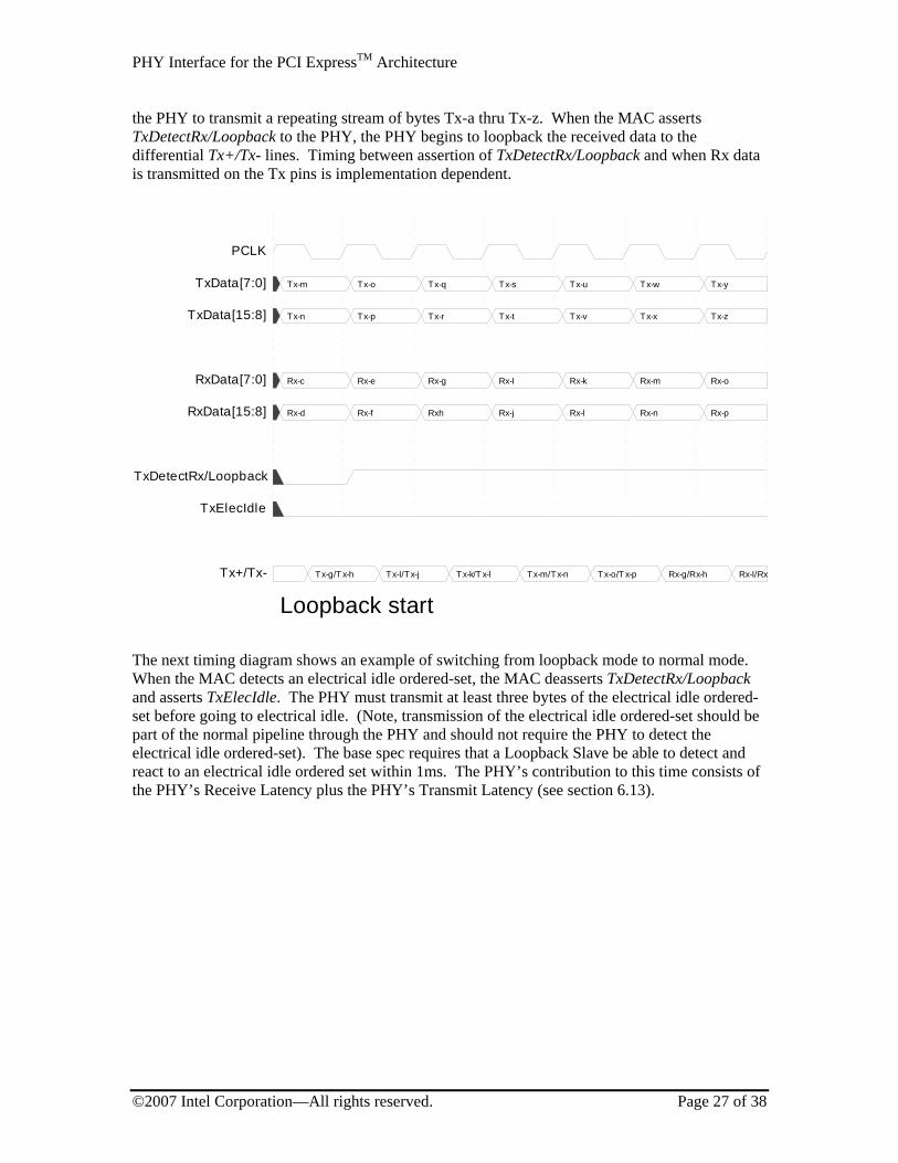
PHY Interface for the PCI ExpressTM Architecture
©2007 Intel Corporation—All rights reserved. Page 27 of 38
the PHY to transmit a repeating stream of bytes Tx-a thru Tx-z. When the MAC asserts TxDetectRx/Loopback to the PHY, the PHY begins to loopback the received data to the differential Tx+/Tx- lines. Timing between assertion of TxDetectRx/Loopback and when Rx data is transmitted on the Tx pins is implementation dependent.
Rx-d Rx-f Rxh Rx-j Rx-l Rx-n Rx-p
Rx-c Rx-e Rx-g Rx-I Rx-k Rx-m Rx-o
Tx-n Tx-p Tx-r Tx-t Tx-v Tx-x Tx-z
Tx-g/Tx-h Tx-I/Tx-j Tx-k/T x-l Tx-m/Tx-n Tx-o/T x-p Rx-g/Rx-h Rx-I/Rx
Tx-m Tx-o Tx-q Tx-s Tx-u Tx-w Tx-y
Loopback start
PCLK
TxData[7:0]
TxData[15:8]
RxData[7:0]
RxData[15:8]
TxDetectRx/Loopback
TxElecIdle
Tx+/Tx-
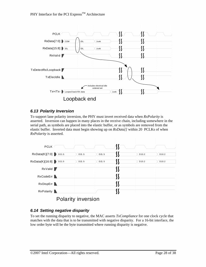
The next timing diagram shows an example of switching from loopback mode to normal mode. When the MAC detects an electrical idle ordered-set, the MAC deasserts TxDetectRx/Loopback and asserts TxElecIdle. The PHY must transmit at least three bytes of the electrical idle ordered-set before going to electrical idle. (Note, transmission of the electrical idle ordered-set should be part of the normal pipeline through the PHY and should not require the PHY to detect the electrical idle ordered-set). The base spec requires that a Loopback Slave be able to detect and react to an electrical idle ordered set within 1ms. The PHY’s contribution to this time consists of the PHY’s Receive Latency plus the PHY’s Transmit Latency (see section 6.13).
PHY Interface for the PCI ExpressTM Architecture
©2007 Intel Corporation—All rights reserved. Page 28 of 38
Looped back RX data Junk
IDL IDL Junk
COM IDL Junk
Loopback end
PCLK
RxData[7:0]
RxData[15:8]
RxValid
TxDetectRx/Loopback
TxElecIdle
Tx+/Tx-
Includes electrical idleordered set
6.13 Polarity Inversion To support lane polarity inversion, the PHY must invert received data when RxPolarity is asserted. Inversion can happen in many places in the receive chain, including somewhere in the serial path, as symbols are placed into the elastic buffer, or as symbols are removed from the elastic buffer. Inverted data must begin showing up on RxData[] within 20 PCLKs of when RxPolarity is asserted.
D21.5 D21 .5 D21. 5 D10.2 D10.2
D21.5 D21 .5 D21. 5 D10.2 D10.2
Polarity inversion
PCLK
RxData(K)[7:0]
RxData(K)[16:8]
RxValid
RxCodeErr
RxDispErr
RxPolarity
6.14 Setting negative disparity To set the running disparity to negative, the MAC asserts TxCompliance for one clock cycle that matches with the data that is to be transmitted with negative disparity. For a 16-bit interface, the low order byte will be the byte transmitted where running disparity is negative.
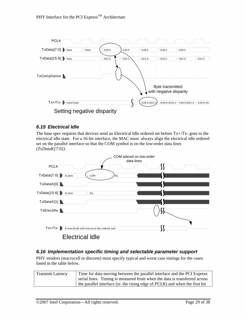
PHY Interface for the PCI ExpressTM Architecture
©2007 Intel Corporation—All rights reserved. Page 29 of 38
Data D21.5 D10.2 D21.5 D10.2 D21.5 D10.2
Data Data K28.5 K28.5 K28.5 K28.5 K28.5
Val id Data K28.5-/D21.5 K28.5+/D10.2 K28.5-/D21.5 K28.5+/D1
Loopback end
PCLK
TxData[7:0]
TxData[15:8]
TxCompliance
Tx+/Tx-
Byte transmittedwith negative disparity
Setting negative disparity
6.15 Electrical Idle The base spec requires that devices send an Electrical Idle ordered set before Tx+/Tx- goes to the electrical idle state. For a 16-bit interface, the MAC must always align the electrical idle ordered set on the parallel interface so that the COM symbol is on the low-order data lines (TxDataK[7:0]).
Active (Ends wi th electrical idle ordered set)
ScZero IDL
ScZero COM IDL
Electrical Idle
PCLK
TxData[7:0]
TxDataK[0]
TxData[15:8]
TxDataK[1]
TxElecIdle
Tx+/Tx-
COM placed on low-orderdata lines
6.16 Implementation specific timing and selectable parameter support PHY vendors (macrocell or discrete) must specify typical and worst case timings for the cases listed in the table below. Transmit Latency Time for data moving between the parallel interface and the PCI Express
serial lines. Timing is measured from when the data is transferred across the parallel interface (ie. the rising edge of PCLK) and when the first bit
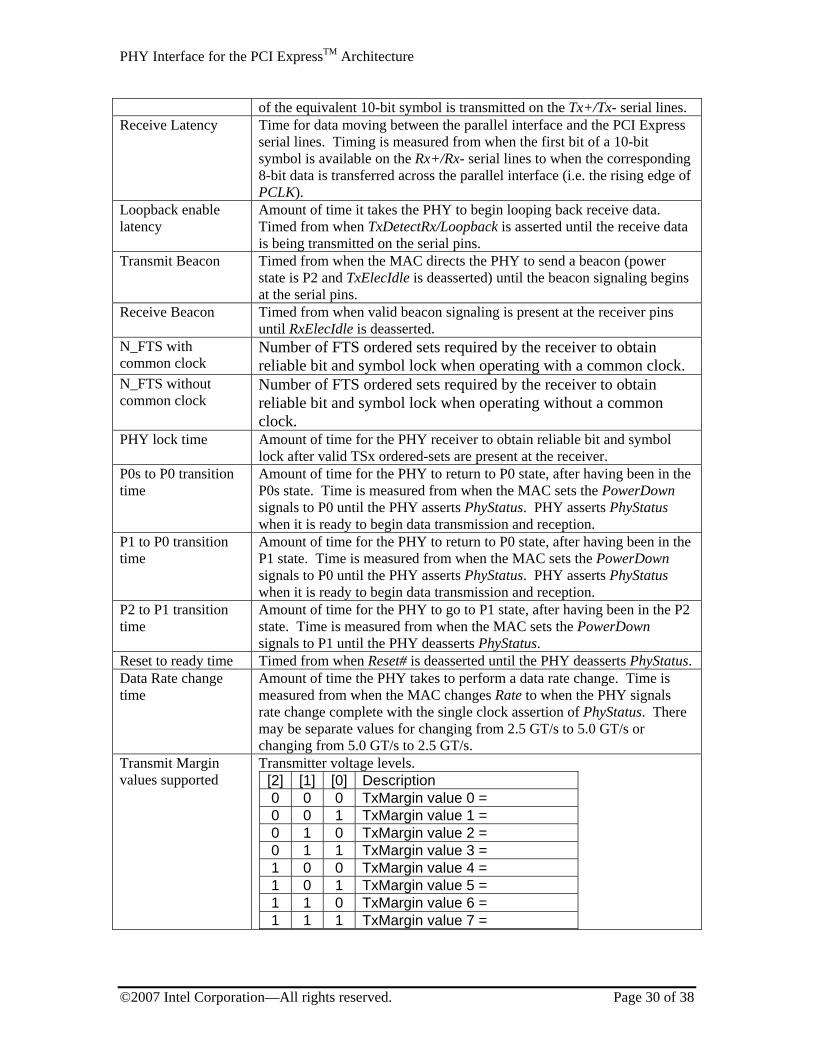
PHY Interface for the PCI ExpressTM Architecture
©2007 Intel Corporation—All rights reserved. Page 30 of 38
of the equivalent 10-bit symbol is transmitted on the Tx+/Tx- serial lines. Receive Latency Time for data moving between the parallel interface and the PCI Express
serial lines. Timing is measured from when the first bit of a 10-bit symbol is available on the Rx+/Rx- serial lines to when the corresponding 8-bit data is transferred across the parallel interface (i.e. the rising edge of PCLK).
Loopback enable latency
Amount of time it takes the PHY to begin looping back receive data. Timed from when TxDetectRx/Loopback is asserted until the receive data is being transmitted on the serial pins.
Transmit Beacon Timed from when the MAC directs the PHY to send a beacon (power state is P2 and TxElecIdle is deasserted) until the beacon signaling begins at the serial pins.
Receive Beacon Timed from when valid beacon signaling is present at the receiver pins until RxElecIdle is deasserted.
N_FTS with common clock
Number of FTS ordered sets required by the receiver to obtain reliable bit and symbol lock when operating with a common clock.
N_FTS without common clock
Number of FTS ordered sets required by the receiver to obtain reliable bit and symbol lock when operating without a common clock.
PHY lock time Amount of time for the PHY receiver to obtain reliable bit and symbol lock after valid TSx ordered-sets are present at the receiver.
P0s to P0 transition time
Amount of time for the PHY to return to P0 state, after having been in the P0s state. Time is measured from when the MAC sets the PowerDown signals to P0 until the PHY asserts PhyStatus. PHY asserts PhyStatus when it is ready to begin data transmission and reception.
P1 to P0 transition time
Amount of time for the PHY to return to P0 state, after having been in the P1 state. Time is measured from when the MAC sets the PowerDown signals to P0 until the PHY asserts PhyStatus. PHY asserts PhyStatus when it is ready to begin data transmission and reception.
P2 to P1 transition time
Amount of time for the PHY to go to P1 state, after having been in the P2 state. Time is measured from when the MAC sets the PowerDown signals to P1 until the PHY deasserts PhyStatus.
Reset to ready time Timed from when Reset# is deasserted until the PHY deasserts PhyStatus. Data Rate change time
Amount of time the PHY takes to perform a data rate change. Time is measured from when the MAC changes Rate to when the PHY signals rate change complete with the single clock assertion of PhyStatus. There may be separate values for changing from 2.5 GT/s to 5.0 GT/s or changing from 5.0 GT/s to 2.5 GT/s.
Transmit Margin values supported
Transmitter voltage levels. [2] [1] [0] Description 0 0 0 TxMargin value 0 = 0 0 1 TxMargin value 1 = 0 1 0 TxMargin value 2 = 0 1 1 TxMargin value 3 = 1 0 0 TxMargin value 4 = 1 0 1 TxMargin value 5 = 1 1 0 TxMargin value 6 = 1 1 1 TxMargin value 7 =
PHY Interface for the PCI ExpressTM Architecture
©2007 Intel Corporation—All rights reserved. Page 31 of 38
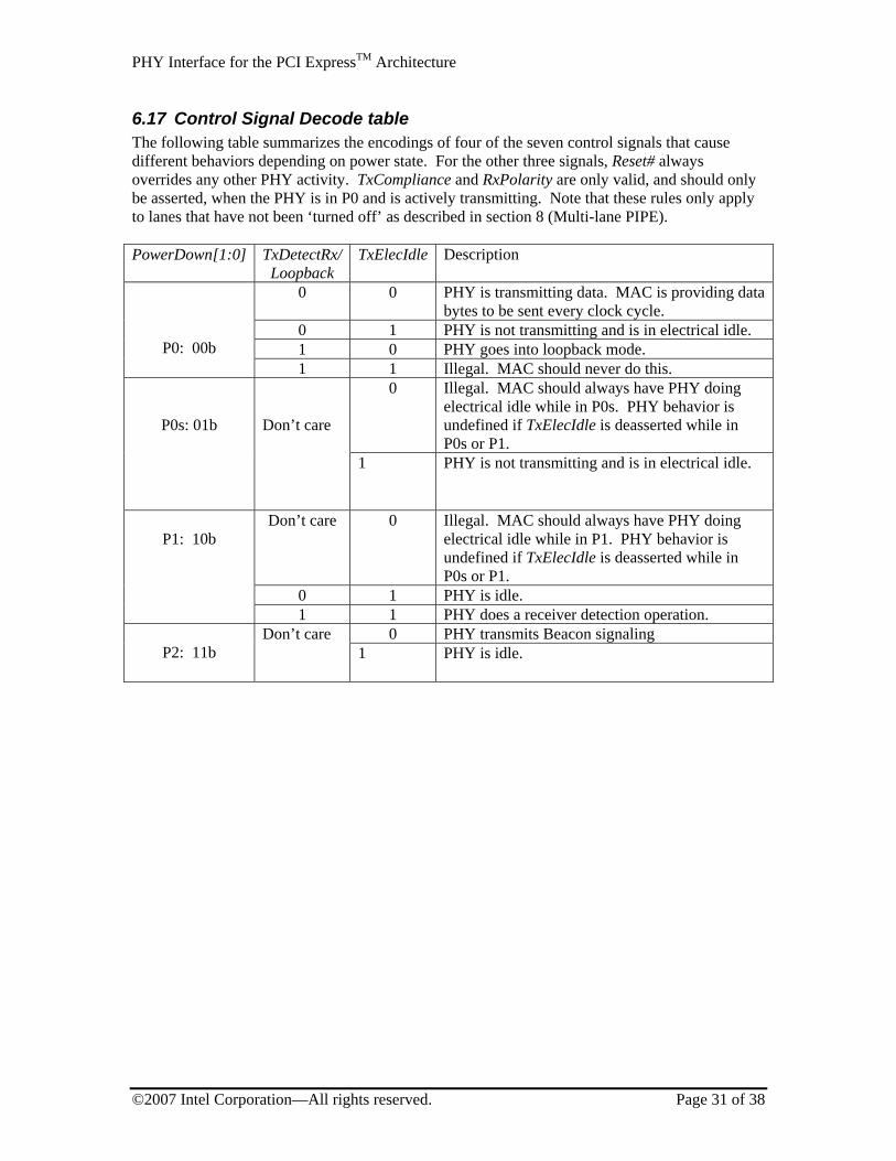
6.17 Control Signal Decode table The following table summarizes the encodings of four of the seven control signals that cause different behaviors depending on power state. For the other three signals, Reset# always overrides any other PHY activity. TxCompliance and RxPolarity are only valid, and should only be asserted, when the PHY is in P0 and is actively transmitting. Note that these rules only apply to lanes that have not been ‘turned off’ as described in section 8 (Multi-lane PIPE). PowerDown[1:0] TxDetectRx/
Loopback TxElecIdle Description
0 0 PHY is transmitting data. MAC is providing data bytes to be sent every clock cycle.
0 1 PHY is not transmitting and is in electrical idle. 1 0 PHY goes into loopback mode.
P0: 00b 1 1 Illegal. MAC should never do this.
0 Illegal. MAC should always have PHY doing electrical idle while in P0s. PHY behavior is undefined if TxElecIdle is deasserted while in P0s or P1.
P0s: 01b
Don’t care
1 PHY is not transmitting and is in electrical idle.
Don’t care 0 Illegal. MAC should always have PHY doing electrical idle while in P1. PHY behavior is undefined if TxElecIdle is deasserted while in P0s or P1.
0 1 PHY is idle.
P1: 10b
1 1 PHY does a receiver detection operation. 0 PHY transmits Beacon signaling
P2: 11b Don’t care
1 PHY is idle.
PHY Interface for the PCI ExpressTM Architecture
©2007 Intel Corporation—All rights reserved. Page 32 of 38
6.18 Recommended synchronous signal timings To improve interoperability between MACs and PHYs from different vendors the following timings for synchronous signals is recommended:
Setup time for input signals No greater than 25% of cycle time Hold time for input signals 0ns PCLK to data valid for outputs No greater than 25% of cycle time
7 Sample Operational Sequences These sections show sample timing sequences for some of the more common PCI Express operations. These are sample sequences and timings and are not required operation.
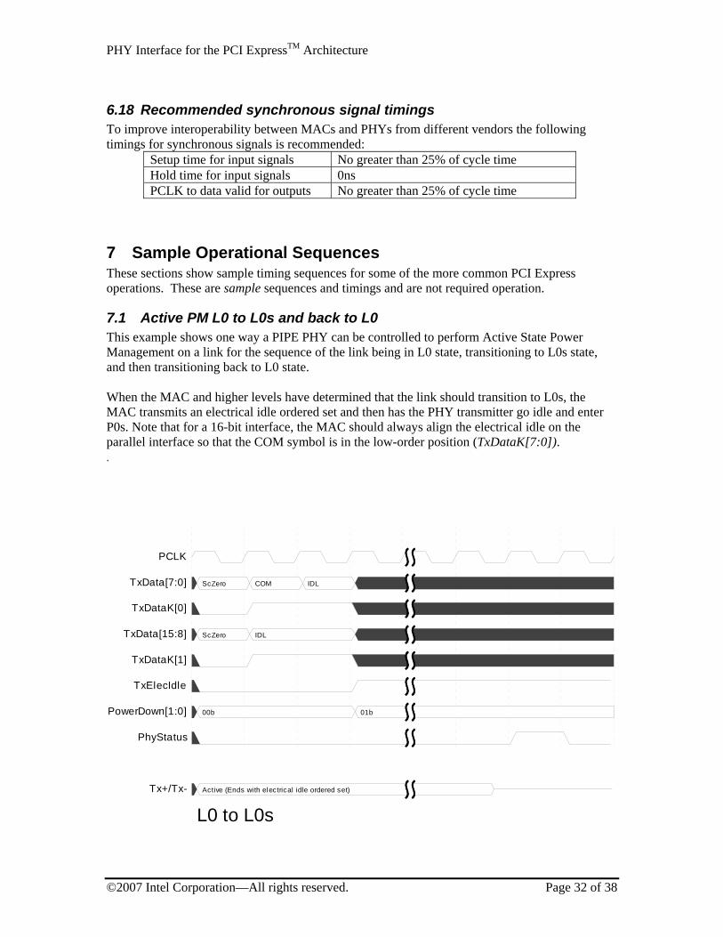
7.1 Active PM L0 to L0s and back to L0 This example shows one way a PIPE PHY can be controlled to perform Active State Power Management on a link for the sequence of the link being in L0 state, transitioning to L0s state, and then transitioning back to L0 state. When the MAC and higher levels have determined that the link should transition to L0s, the MAC transmits an electrical idle ordered set and then has the PHY transmitter go idle and enter P0s. Note that for a 16-bit interface, the MAC should always align the electrical idle on the parallel interface so that the COM symbol is in the low-order position (TxDataK[7:0]). .
00b 01b
ScZero IDL
Active (Ends with electrical idle ordered set)
ScZero COM IDL
L0 to L0s
PCLK
TxData[7:0]
TxDataK[0]
TxData[15:8]
TxDataK[1]
TxElecIdle
PowerDown[1:0]
PhyStatus
Tx+/Tx-
PHY Interface for the PCI ExpressTM Architecture
©2007 Intel Corporation—All rights reserved. Page 33 of 38
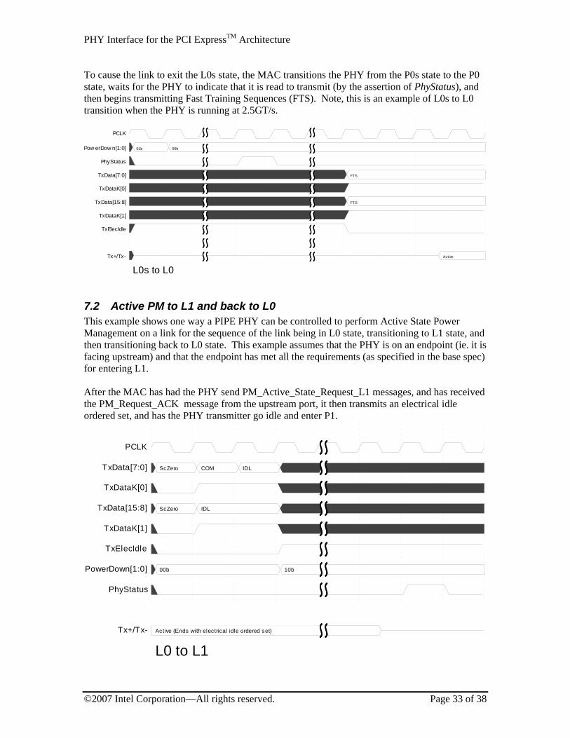
To cause the link to exit the L0s state, the MAC transitions the PHY from the P0s state to the P0 state, waits for the PHY to indicate that it is read to transmit (by the assertion of PhyStatus), and then begins transmitting Fast Training Sequences (FTS). Note, this is an example of L0s to L0 transition when the PHY is running at 2.5GT/s.
01b 00b
FTS
Active
FTS
L0s to L0
PCLK
Pow erDow n[1:0]
PhyStatus
TxData[7:0]
TxDataK[0]
TxData[15:8]
TxDataK[1]
TxElecIdle
Tx+/Tx-
7.2 Active PM to L1 and back to L0 This example shows one way a PIPE PHY can be controlled to perform Active State Power Management on a link for the sequence of the link being in L0 state, transitioning to L1 state, and then transitioning back to L0 state. This example assumes that the PHY is on an endpoint (ie. it is facing upstream) and that the endpoint has met all the requirements (as specified in the base spec) for entering L1. After the MAC has had the PHY send PM_Active_State_Request_L1 messages, and has received the PM_Request_ACK message from the upstream port, it then transmits an electrical idle ordered set, and has the PHY transmitter go idle and enter P1.
00b 10b
ScZero IDL
Active (Ends with electrical idle ordered set)
ScZero COM IDL
L0 to L1
PCLK
TxData[7:0]
TxDataK[0]
TxData[15:8]
TxDataK[1]
TxElecIdle
PowerDown[1:0]
PhyStatus
Tx+/Tx-
PHY Interface for the PCI ExpressTM Architecture
©2007 Intel Corporation—All rights reserved. Page 34 of 38
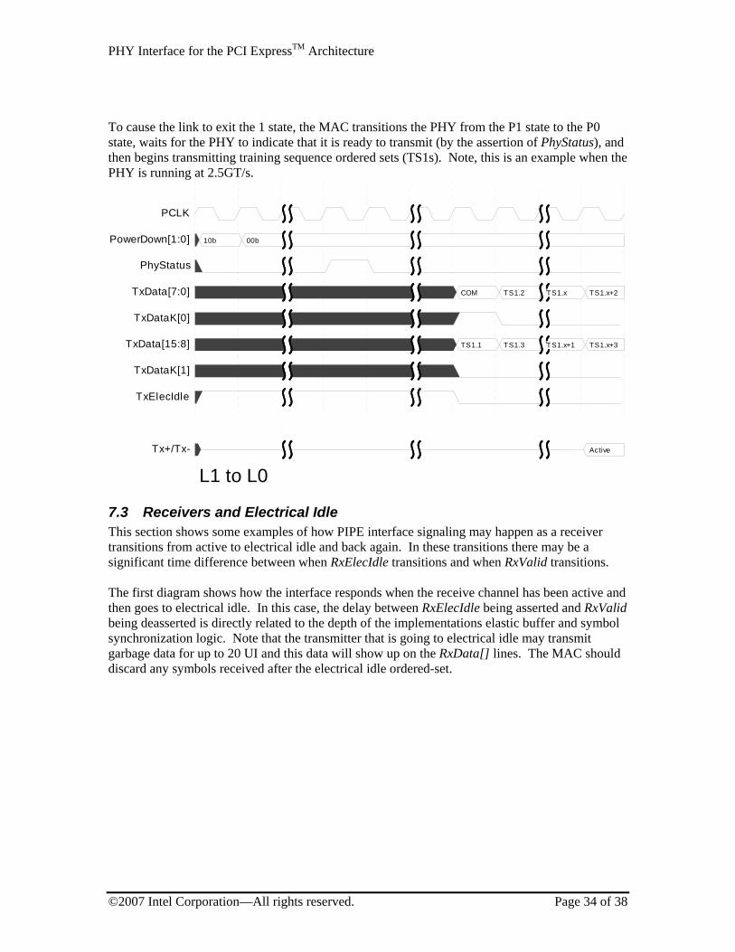
To cause the link to exit the 1 state, the MAC transitions the PHY from the P1 state to the P0 state, waits for the PHY to indicate that it is ready to transmit (by the assertion of PhyStatus), and then begins transmitting training sequence ordered sets (TS1s). Note, this is an example when the PHY is running at 2.5GT/s.
10b 00b
TS1.1 TS1.3 TS1.x+1 TS1.x+3
Active
COM TS1.2 TS1.x TS1.x+2
L1 to L0
PCLK
PowerDown[1:0]
PhyStatus
TxData[7:0]
TxDataK[0]
TxData[15:8]
TxDataK[1]
TxElecIdle
Tx+/Tx-
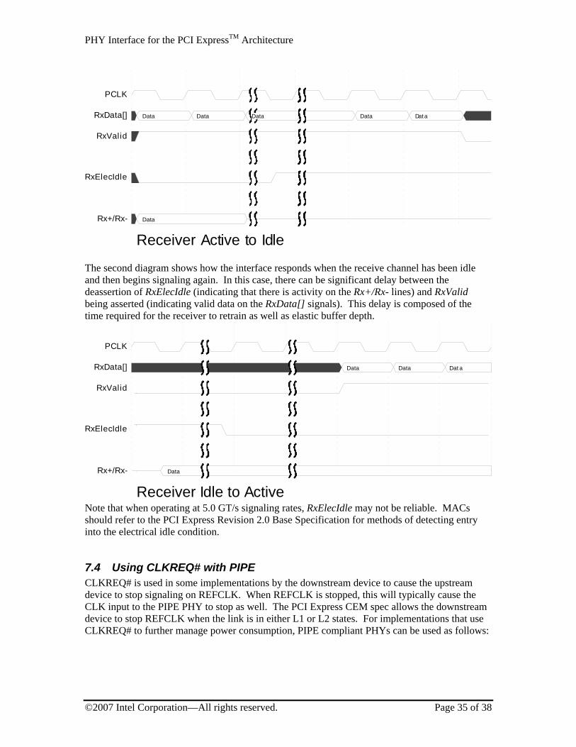
7.3 Receivers and Electrical Idle This section shows some examples of how PIPE interface signaling may happen as a receiver transitions from active to electrical idle and back again. In these transitions there may be a significant time difference between when RxElecIdle transitions and when RxValid transitions. The first diagram shows how the interface responds when the receive channel has been active and then goes to electrical idle. In this case, the delay between RxElecIdle being asserted and RxValid being deasserted is directly related to the depth of the implementations elastic buffer and symbol synchronization logic. Note that the transmitter that is going to electrical idle may transmit garbage data for up to 20 UI and this data will show up on the RxData[] lines. The MAC should discard any symbols received after the electrical idle ordered-set.
PHY Interface for the PCI ExpressTM Architecture
©2007 Intel Corporation—All rights reserved. Page 35 of 38
Data
Data Data Data Data Dat a
Receiver Active to Idle
PCLK
RxData[]
RxValid
RxElecIdle
Rx+/Rx-
The second diagram shows how the interface responds when the receive channel has been idle and then begins signaling again. In this case, there can be significant delay between the deassertion of RxElecIdle (indicating that there is activity on the Rx+/Rx- lines) and RxValid being asserted (indicating valid data on the RxData[] signals). This delay is composed of the time required for the receiver to retrain as well as elastic buffer depth.
Data
Data Data Dat a
Receiver Idle to Active
PCLK
RxData[]
RxValid
RxElecIdle
Rx+/Rx-
Note that when operating at 5.0 GT/s signaling rates, RxElecIdle may not be reliable. MACs should refer to the PCI Express Revision 2.0 Base Specification for methods of detecting entry into the electrical idle condition.
7.4 Using CLKREQ# with PIPE CLKREQ# is used in some implementations by the downstream device to cause the upstream device to stop signaling on REFCLK. When REFCLK is stopped, this will typically cause the CLK input to the PIPE PHY to stop as well. The PCI Express CEM spec allows the downstream device to stop REFCLK when the link is in either L1 or L2 states. For implementations that use CLKREQ# to further manage power consumption, PIPE compliant PHYs can be used as follows:
PHY Interface for the PCI ExpressTM Architecture
©2007 Intel Corporation—All rights reserved. Page 36 of 38
The general usage model is that to stop REFCLK the MAC puts the PHY into the P2 power state, then deasserts CLKREQ#. To get the REFCLK going again, the MAC asserts CLKREQ#, and then after some PHY and implementation specific time, the PHY is ready to use again. CLKREQ# in L1 If the MAC is moving the link to the L1 state and intends to deassert CLKREQ# to stop REFCLK, then the MAC follows the proper sequence to get the link to L1, but instead of finishing by transitioning the PHY to P1, the MAC transition the PHY to P2. Then the MAC deasserts CLKREQ#. When the MAC wants to get the link alive again, it can:
• Assert CLKREQ# • Wait for REFCLK to be stable (implementation specific) • Wait for the PHY to be ready (PHY specific) • Transition the PHY to P0 state and begin training.
CLKREQ# in L2 If the MAC is moving the link to the L1 state and intends to deassert CLKREQ# to stop REFCLK, then the MAC follows the proper sequence to get the link to L2. Then the MAC deasserts CLKREQ#. When the MAC wants to get the link alive again, it can:
• Assert CLKREQ# • Wait for REFCLK to be stable (implementation specific) • Wait for the PHY to be ready (PHY specific) • Transition the PHY to P0 state and begin training.
Delayed CLKREQ# in L1 The MAC may want to stop REFCLK after the link has been in L1 and idle for awhile. In this case, the PHY is in the P1 state and the MAC must transition the PHY into the P0 state, and then the P2 state before deasserting CLKREQ#. Getting the link operational again is the same as the preceding cases.
PHY Interface for the PCI ExpressTM Architecture
©2007 Intel Corporation—All rights reserved. Page 37 of 38
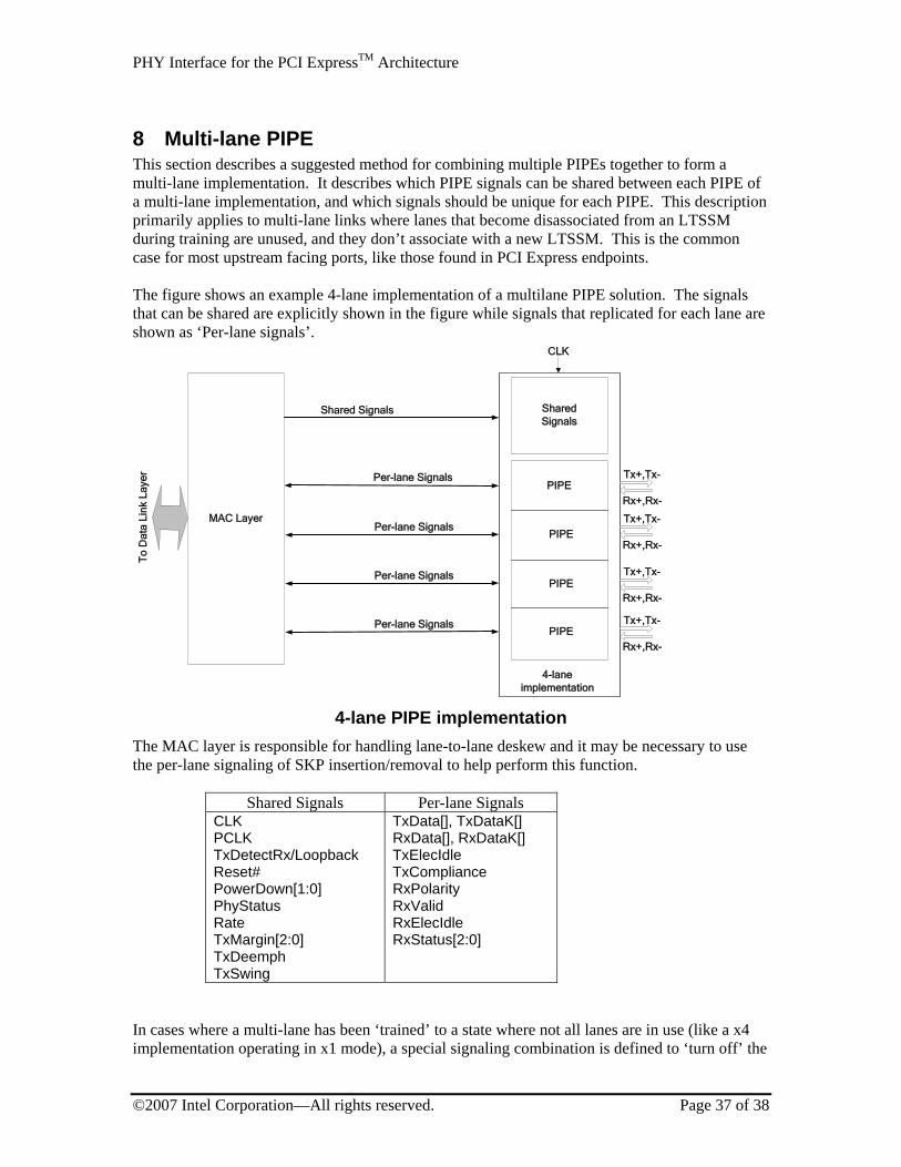
8 Multi-lane PIPE This section describes a suggested method for combining multiple PIPEs together to form a multi-lane implementation. It describes which PIPE signals can be shared between each PIPE of a multi-lane implementation, and which signals should be unique for each PIPE. This description primarily applies to multi-lane links where lanes that become disassociated from an LTSSM during training are unused, and they don’t associate with a new LTSSM. This is the common case for most upstream facing ports, like those found in PCI Express endpoints. The figure shows an example 4-lane implementation of a multilane PIPE solution. The signals that can be shared are explicitly shown in the figure while signals that replicated for each lane are shown as ‘Per-lane signals’.
MAC Layer
PIPEPer-lane Signals
To
Dat
a Li
nk L
ayer Tx+,Tx-
Rx+,Rx-
CLK
SharedSignals
PIPE
PIPE
PIPE
Per-lane Signals
Per-lane Signals
Per-lane Signals
Tx+,Tx-
Rx+,Rx-
Tx+,Tx-
Rx+,Rx-
Tx+,Tx-
Rx+,Rx-
4-laneimplementation
Shared Signals
4-lane PIPE implementation
The MAC layer is responsible for handling lane-to-lane deskew and it may be necessary to use the per-lane signaling of SKP insertion/removal to help perform this function.
Shared Signals Per-lane Signals CLK PCLK TxDetectRx/Loopback Reset# PowerDown[1:0] PhyStatus Rate TxMargin[2:0] TxDeemph TxSwing
TxData[], TxDataK[] RxData[], RxDataK[] TxElecIdle TxCompliance RxPolarity RxValid RxElecIdle RxStatus[2:0]
In cases where a multi-lane has been ‘trained’ to a state where not all lanes are in use (like a x4 implementation operating in x1 mode), a special signaling combination is defined to ‘turn off’ the
PHY Interface for the PCI ExpressTM Architecture
©2007 Intel Corporation—All rights reserved. Page 38 of 38
unused lanes allowing them to conserve as much power as the implementation allows. This special ‘turn off’ signaling is done using the TxElecIdle and TxCompliance signals. When both are asserted, that PHY can immediately be considered ‘turned off’ and can take whatever power saving measures are appropriate. The PHY ignores any other signaling from the MAC (with the exception of Reset# assertion) while it is ‘turned off’. Similarly, the MAC should ignore any signaling from the PHY when the PHY is ‘turned off’. There is no ‘handshake’ back to the MAC to indicate that the PHY has reached a ‘turned off’ state. There are two normal cases when a lane can get turned off:
1. During LTSSM Detect state, the MAC discovers that there is no receiver present and will ‘turn off’ the lane.
2. During LTSSM Configuration state (specifically Configuration.Complete), the MAC will ‘turn off’ any lanes that didn’t become part of the configured link.
As an example, both of these cases could occur when a x4 device is plugged into a x8 slot. The upstream device (the one with the x8 port) will not discover receiver terminations on four of its lanes so it will turn them off. Training will occur on the remaining 4 lanes, and let’s suppose that the x8 device cannot operate in x4 mode, so the link configuration process will end up settling on x1 operation for the link. Then both the upstream and downstream devices will ‘turn off’ all but the one lane configured in the link. When the MAC wants to get ‘turned off’ lanes back into an operational state, there are two cases that need to be considered:
1. If the MAC wants to reset the multi-lane PIPE, it asserts Reset# and drives other interface signals to their proper states for reset (see section 6.2). Note that this stops signaling ‘turned off’ to all lanes because TxCompliance is deasserted during reset. The multi-lane PHY asserts PhyStatus in response to Reset# being asserted, and will deassert PhyStatus when PCLK is stable.
2. When normal operation on the active lanes causes those lanes to transition to the LTSSM Detect state, then the MAC sets the PowerDown[1:0] signals to the P1 PHY power state at the same time that it deasserts ‘turned off’ signaling to the inactive lanes. Then as with normal transitions to the P1 state, the multi-lane PHY will assert PhyStatus for one clock when all internal PHYs are in the P1 state and PCLK is stable.