Photovoltaic Spectral Response EQE (IPCE), IQE standard spectral range of 300-1100nm, may easily be...
8
PVE300 Photovoltaic Spectral Response EQE (IPCE), IQE
Transcript of Photovoltaic Spectral Response EQE (IPCE), IQE standard spectral range of 300-1100nm, may easily be...

PVE300 Photovoltaic Spectral Response
EQE (IPCE), IQE
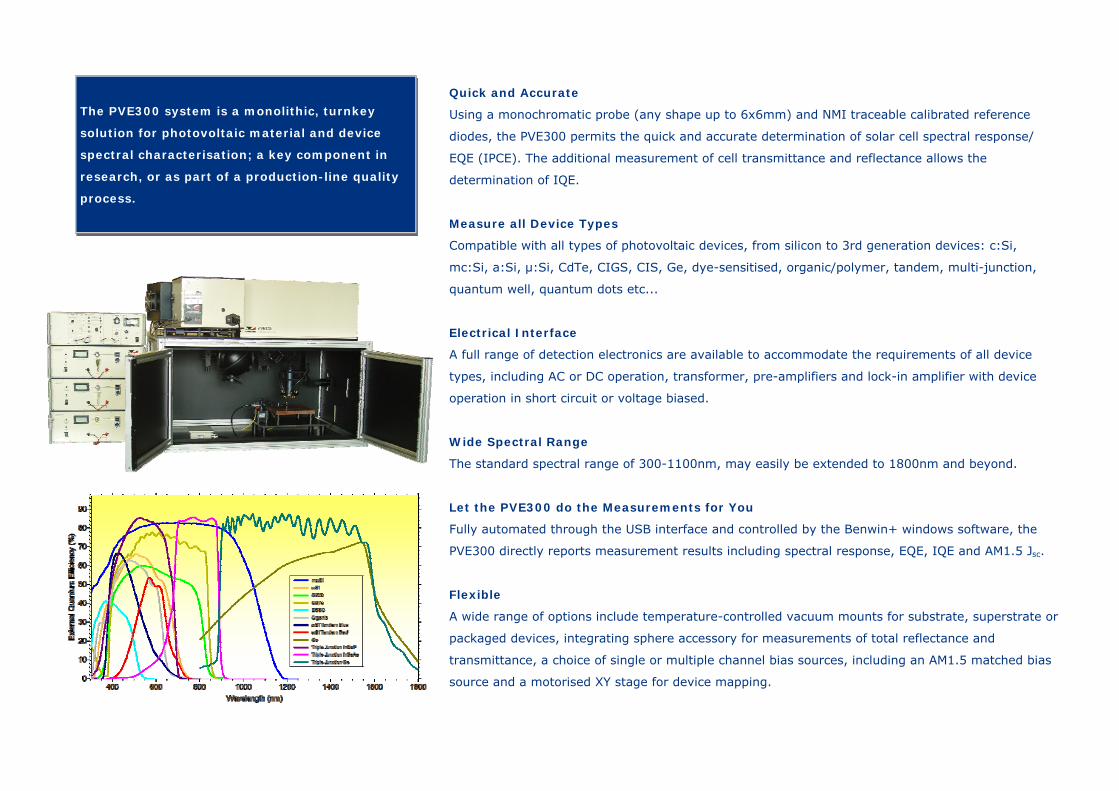
Quick and Accurate
Using a monochromatic probe (any shape up to 6x6mm) and NMI traceable calibrated reference
diodes, the PVE300 permits the quick and accurate determination of solar cell spectral response/
EQE (IPCE). The additional measurement of cell transmittance and reflectance allows the
determination of IQE.
Measure all Device Types
Compatible with all types of photovoltaic devices, from silicon to 3rd generation devices: c:Si,
mc:Si, a:Si, µ:Si, CdTe, CIGS, CIS, Ge, dye-sensitised, organic/polymer, tandem, multi-junction,
quantum well, quantum dots etc...
Electrical Interface
A full range of detection electronics are available to accommodate the requirements of all device
types, including AC or DC operation, transformer, pre-amplifiers and lock-in amplifier with device
operation in short circuit or voltage biased.
Wide Spectral Range
The standard spectral range of 300-1100nm, may easily be extended to 1800nm and beyond.
Let the PVE300 do the Measurements for You
Fully automated through the USB interface and controlled by the Benwin+ windows software, the
PVE300 directly reports measurement results including spectral response, EQE, IQE and AM1.5 Jsc.
Flexible
A wide range of options include temperature-controlled vacuum mounts for substrate, superstrate or
packaged devices, integrating sphere accessory for measurements of total reflectance and
transmittance, a choice of single or multiple channel bias sources, including an AM1.5 matched bias
source and a motorised XY stage for device mapping.
The PVE300 system is a monolithic, turnkey
solution for photovoltaic material and device
spectral characterisation; a key component in
research, or as part of a production-line quality
process.

Overview of Operation The sample under test is mounted horizontally on a temperature
controlled vacuum mount for thermal stability. A monochromatic
probe is made to be incident upon the sample under test; at
each wavelength is measured the photocurrent generated by the
device. Having measured the beam power with a detector of
known responsivity, spectral response and EQE can be directly
obtained. The manner in which the device photocurrent is
measured, and the conditions under which this test is performed,
depends upon the type of device under test, described overleaf.
In many instances it is desirable to operate the cell in the
presence of a bias of one sun (1000 W m-2) to simulate use
conditions; indeed the use of such, with appropriate filtering, is
essential in the measurement of multiple junction cells to ensure
that the subcell under test be current limiting. In the case of
multiple junction and thin film devices, a voltage bias may also
be required.
Intervening a divert mirror in the beam relays the
monochromatic probe to a 6” diameter integrating sphere,
mounted on an optical rail to the upper of the PVE300 chamber,
for the measurement of device total reflectance and total
transmittance (where required). The EQE may be modified by
these latter measurements to determine the more fundamental
parameter of IQE.
Determination of spectral response (SR, A W-1) & external quantum
efficiency (EQE/IPCE, %)
Determination of total reflectance/transmittance (R/T), to modify EQE to yield internal quantum efficiency
(IQE, %)
Spectral Response Reflectance
EQE IQE

Chopped Monochromatic Probe Source A monochromatic probe is assembled from a TMc300, 300mm focal length monochromator and a dual Xenon/ quartz halogen light source, providing optimum illumination from the UV to the NIR. The dual source may be fitted with a 218 optical chopper (10 Hz-2 kHz) or a shutter-based 0-2Hz DC chopper. The 218 may be made to be arrestable to permit migration from the AC to DC mode.
PVE300 System Components
DTR6 Integrating Sphere The DTR6 integrating sphere is mounted on a optical rail to the upper of the PVE300 chamber to permit the measurement of total reflectance and total transmittance.
Detection Electronics The 417 unit houses the detection electronics of the PVE300 system. The detection electronics employed depends on the nature of the device under test, discussed in detail overleaf.
474– Transformer/ low noise amplifier Front-end for lock-in amplifier Transformer couples only AC signal Cell operated in short circuit conditions or under voltage bias Transformer followed by low-noise amplifier
477– AC trans-impedance pre-amplifier Front-end for lock-in amplifier Six decades of gain Cell operated in short circuit conditions Useful in measuring experimental devices and cell reflectance/ transmittance
497– DC/AC trans-impedance pre-amplifier & ADC Front-end for lock-in amplifier or main detection electronics in DC mode Six decades of gain > 14 bit ADC Cell operated in short circuit conditions
495– Phase insensitive lock-in amplifier Recover optically chopped signal Operation 10-2000Hz Measures two orthogonal phases to return vector sum > 14 bit ADC
218– Optical Chopper Controller Controller for optical chopper housed in dual source Reference output for lock-in amplifier
Constant Current Power Supply A 605 constant current supply is required for each light source (xenon, quartz halogen and solar simulator). The excellent stability of the 605 ensures constant lamp out-put.
The PVE300 reunites the probe and bias sources at the sample plane where the temperature-controlled vacuum mount is situated. A diverting mirror is inserted to relay the probe to an integrating sphere for the measurement of transmittance and reflectance.

Relay Optic A mirror-based relay optic images the apertured monochromator exit port onto the sample plane, to provide a probe of any shape up to 6x6mm. Where the use of an aperture would exceed the desired measurement bandwidth, the said aperture may be mounted outside the exit slit and the monochromator translated on rails to move the aperture to the imaged plane.
Solar Simulator A variable intensity quartz halogen-based solar simulator with computer controlled shutter is mounted to the wall of the PVE300. Light is transported via six-branch fibre to ensure uniform illumination in the sample plane. Options include filter positions, class B AM1.5 solar simulator and multiple simulators for the measurement of multiple junction devices
Reference Detectors The system is calibrated with reference to NMI traceable calibrated photodiodes (silicon 300-1100nm; germanium 800-1800nm).
Temperature Controlled Vacuum Mount This 200x200mm mount provides the user with a convenient manner of electrical probing and allows controlling sample temperature, by a quartet of Peltier devices, from 10-60°C , to counter the heating effects attendant to use of a solar simulator, or for material investigation. For superstrate or packaged devices, alternative mounting and probing schemes are available. An accompanying control unit houses the vacuum and water pumps and the bi-polar temperature control electronics.
Software Control The PVE300 is entirely automated through the USB interface and controlled through the Benwin+ windows application.
The easy user interface allows quick and easy system calibration, measurements of spectral response, reflectance and transmittance, determination of EQE/IQE and switching bias sources. Data may be analysed directly or exported to another platform as required.

In general, standard techniques require that the spectral response of solar cells be tested under light biasing at 1000 W m-2 to simulate use conditions†. This
presents the problem of discriminating the photocurrent generated by the monochromatic probe from that generated by the solar simulator. In most cases,
this situation may be circumvented by optically chopping the monochromatic probe and recovering the AC signal with a lock-in amplifier having either a
transformer or trans-impedance amplifier front-end. Whilst the former input stage is preferred- since it does not pass the DC signal, the AC signal can be
given maximum possible gain- it only functions at elevated frequency, incompatible with certain types of cell. Indeed, in the case of certain DSSC cells, with
particularly slow electron transport, recourse is made to the use of a DC monochromatic probe and detection. The following are the recommended routes for
testing the solar cells of today.
Semiconductor and Organic Solar Cells 474 Transformer & 495 Lock-in Amplifier
The fast electron transport mechanisms in most semiconductor and some organic cells permit exploitation of the preferred transformer coupling method. The monochromatic probe beam is optically chopped at a frequency of 600 Hz and the cell under test illuminated with a one sun solar bias. The solar cell output is coupled by the 474 transformer, which passes only the optically chopped signal. This signal is amplified and passed to the lock-in amplifier. The device is operated under short circuit conditions. This technique is recommended for all semiconductor (c:Si, mc:Si, a:Si, µ:Si, CdTe, CIGS, CIS, Ge, tandem, multi-junction, quantum well, quantum dots) and some organic cells.
Organic and DSSC Solar Cells 477/497 Pre-amplifier & 495 Lock-In
Amplifier Where device response is slow, recourse is made in the first instance to reduced chopping frequency and the use of a trans-impedance amplifier front-end to the lock-in amplifier. The monochromatic probe beam is optically chopped at a frequency of >10 Hz and the cell under test illuminated with one sun solar bias (or less to improve signal to noise). The solar cell output is passed through the 477/497 trans-impedance amplifier prior to being passed to the lock-in amplifier. The device is operated under short circuit conditions. This technique may be applied to organic and some DSSC cells.
DSSC Solar Cells 497 and DC chopper
Due to carrier transport mechanisms at play in DSSC cells, it may be found necessary to operate these cells at much slower chopping frequencies or in the DC regime. The monochromatic probe beam is either run DC or optically chopped up to 2Hz, and the cell illuminated with a reduced level of solar bias. The solar cell output is passed through a trans-impedance amplifier and the cell response recorded as a shutter in the dual source switches on and off the monochromatic probe. The device is operated under short-circuit conditions. This technique may be applied to DSSC technologies.
The Choice of Correct Detection Electronics
†IEC60904-8/ ASTM E1021 – 06/ ASTM E2236-05

PVE300 System Options This PVE300 has been designed as a modular and configurable system to adapt to the measurement requirements of the PV technology to be studied. The
following provides a guide to the options available to enhance the functionality of the system.
Spectral Range The TMc300 monochromator may be fitted with up to three diffraction gratings to allow measurement over wide spectral range in a single scan. The standard range of 300-1100nm may be extended to a maximum range of 250-2500nm.
Integrating Sphere The DTR6 integrating sphere is used to collect the total transmitted or reflected light from a sample (specular inclusive or exclusive), with which information may be modified the device EQE to determine the more fundamental parameter of IQE.
Temperature Controlled Vacuum Mount Whilst the electrical and thermal connection of substrate devices is relatively trivial, the same cannot be said of superstrate or packaged devices. With an in-house design service, Bentham can design a mount suitable for your application.
DC/ Chopped Monochromatic Probe The monochromatic probe may be operated in the AC or DC regimes with either the 218 optical chopper (10 Hz-2 kHz) or a shutter-based 0-2Hz DC chopper. The 218 may be made to be arrestable to permit migration from the AC to DC mode.
Multiple Light Bias Sources In the measurement of multi-junction devices, multiple solar simulators are required, one to bias the subcell under test at one sun, the other filtered simulator to ensure that the non– tested subcells are sufficiently illuminated that they do not current limit the tested subcell response.
XY Stage Device uniformity and IPCE mapping may be performed with the use of an XY stage, upon which is mounted the temperature-controlled vacuum chuck, and the PVE300 enclosure height extended. The sample position is scanned under the beam and entirely controlled through Benwin+.
Voltage Biasing In the case of multiple junction cells and some thin film device, testing under voltage bias is important. To this end, a Keithley 2400 Source Meter can be connected directly to the transformer primary coil, thereby biasing the device under test.
High Output Monochromatic Light Source For ultimate flexibility in the measurement of multiple junction cells, a high irradiance monochromatic probe, assembled from a 450W xenon lamp and 300mm focal length monochromator provides a tuneable source 300-1100nm.

Monochromatic Probe
Probe light source: 75W Xenon and 100W Quartz halogen
Monochromator configuration:
Triple grating, symmetric, single Czerny-Turner, 300mm focal length
Bandwidth: Adjustable fixed slit, 1-10nm typical
Resolution: 0.3nm (1200g/mm); 0.6nm (600g/mm)
Dispersion: 2.7nm/mm (1200g/mm); 5.4nm/mm (600g/mm)
Wavelength Range: 300-1100nm (1200g/mm ); 1100-2500nm (600g/mm)
Wavelength accuracy: ± 0.2nm (1200g/mm); ± 0.4nm (600g/mm)
Relay Optic: Mirror-based, 1.2x magnification
Probe size: Up to 6x6mm
Temperature-Controlled Vacuum Mount
Temperature control: 4x70W Peltier-based heat pump, water- cooled hot side
Temperature range: 10-60°C
Temperature Feedback: Centrally-positioned sensor situated 3mm below sample plane
Temperature stability: ± 1°C
Solar Simulator
Transport to sample: Branched glass fibre bundle
Bias source irradiance: 0-1.5 suns
Bias source uniformity: ±1% over 1 cm2
Filter Option: Two 50mm square filter holders
Source Options: Quartz halogen/ Xenon/ Class B AM1.5
Automation
Software control: BenWin+ Windows application
Interface: USB
PVE300 Specifications 495 Phase Insensitive Lock-In Amplifier
Frequency Range: 10Hz to 10kHz
Sensitivity: 1mV to 1V in decade steps
Input Impedance: 100MΩ/25pf, pseudo differential
Dynamic Reserve: 40dB
Gain Accuracy: +1%
Gain Stability 200ppm/°C
Phase Control: 0.025° increments plus 90° increments
Output Stability: 5ppm/°C to 500ppm/°C depending on sensitivity
Time Constant: 10ms to 10s.
Phase Display: 3 digit LC display shows current phase setting
477/497 Specification
Gain Ranges: 103-108 V/A
Maximum Input: 10mA
Input Impedance: Virtual ground
Gain Accuracy: +1%
Gain Stability: 200ppm/°C
Output Stability: 5ppm/°C to 500ppm/°C depending on gain range
495/497 ADC
Resolution: 4 ½ digit BCD (0 to 19999) i.e. > 14 bit resolution
Conversion: 100ms
Input Range: -0.2V to 9.8V
Linearity: < 0.025% departure from linearity from zero to full scale
474 Specification
Transformer DC resistance: 0.05Ω
Gain: Trans. ~100x. Amp. 500x
Amplifier bandwidth: 5Hz to >100kHz
Amplifier short circuit input noise: <1nV Hz-1/2 at 1kHz
Amplifier Maximum Output: 10V
Frequency of Operation: 600Hz typical
Minimum responsivity: 0.03 A W-1 nm-1 5nm BW, 2mm probe typ.
Optical Chopper
218 frequency range: 10-2 kHz
DC chopper frequency range: DC-2 Hz
Reference Diodes
Diode & Range: Silicon 300-1100nm; Germanium 800-1800nm
Traceability NPL/ PTB
Voltage Bias (Keithley 2400)
Voltage Range: -20 to 20V
Current Limit: 1A
XY Stage
Travel: 300mm in X & Y
Resolution: 0.1mm
DTR6 Integrating Sphere
Port Size: 15mm Ø (5 &10mm Ø port reducers supplied)
Coating: Ba2SO4
Detector: Silicon/ Germanium/ Silicon-InGaAs sandwich
Contact Us Tel: 00 44 (0) 118 975 1355 Fax: 00 44 (0) 118 931 2971 Email: [email protected] Web: www.bentham.co.uk
Bentham Instruments Limited 2 Boulton Road Reading RG2 0NH United Kingdom