Photovoltaic property of bismuth ferrite thin films and ...
96
This document is downloaded from DR‑NTU (https://dr.ntu.edu.sg) Nanyang Technological University, Singapore. Photovoltaic property of bismuth ferrite thin films and its application in non‑volatile memory Guo, Rui 2013 Guo, R. (2013). Photovoltaic property of bismuth ferrite thin films and its application in non‑volatile memory. Doctoral thesis, Nanyang Technological University, Singapore. https://hdl.handle.net/10356/55058 https://doi.org/10.32657/10356/55058 Downloaded on 02 Apr 2022 02:09:00 SGT
Transcript of Photovoltaic property of bismuth ferrite thin films and ...

This document is downloaded from DR‑NTU (https://dr.ntu.edu.sg)Nanyang Technological University, Singapore.
Photovoltaic property of bismuth ferrite thin filmsand its application in non‑volatile memory
Guo, Rui
2013
Guo, R. (2013). Photovoltaic property of bismuth ferrite thin films and its application innon‑volatile memory. Doctoral thesis, Nanyang Technological University, Singapore.
https://hdl.handle.net/10356/55058
https://doi.org/10.32657/10356/55058
Downloaded on 02 Apr 2022 02:09:00 SGT

PHOTOVOLTAIC PROPERTY OF BISMUTH FERRITE THIN
FILMS AND ITS APPLICATION IN NON-VOLATILE
MEMORY
GUO RUI
SCHOOL OF MATERIALS SCIENCE AND ENGINEERING
2013
PH
OT
OV
OL
TA
IC P
RO
PE
RT
Y O
F B
ISM
UT
H
FE
RR
ITE
TH
IN F
ILM
S A
ND
ITS
AP
PL
ICA
TIO
N A
S
NO
N-V
OL
AT
ILE
PH
OT
OV
OL
TA
IC F
ER
AM
GU
O R
UI
20
13

PHOTOVOLTAIC PROPERTY OF BISMUTH FERRITE THIN
FILMS AND ITS APPLICATION IN NON-VOLATILE
MEMORY
Guo Rui
School of Materials Science and Engineering
A thesis submitted to the Nanyang Technological University
in fulfillment of the requirement for the degree of
Doctor of Philosophy
2013

I
ACKOWLEGEMENT
First of all, I would like to convey my deepest gratitude to my supervisor, associate professor
Wang Junling, for his guidance in my research work during my PhD period. Prof. Wang is an
amazing supervisor, who is not only knowledgeable, but also very helpful to students. His
profound knowledge and preciseness in science enlighten me really a lot. I benefited greatly
from his inspiring ideas, suggestions and the discussions we had. Moreover, during the four
years, I have learnt not only how to do research, but also how to do things. The serious
attitude plus the correct smart ways to do things will make me not afraid of difficulty in my
future life. All of these that I have learnt from Prof. Wang will be a great wealth for the rest
of my life.
Here, I also take the opportunity to thank another amazing professor, my former supervisor,
Yang Jianfeng, who keeps helping and encouraging me all the time. What I have learnt from
Prof. Yang and his help to me benefit me forever.
Secondly, I wish to extend my thanks to all my current and former groupmates. Dr. You Lu
(our best group leader), Dr. Zou Xi, Dr. Zheng Zhaoke, Dr. Wang Baomin, Dr. Ong Hock
Guan, Dr. Chen Weigang, Dr. Zhang Zhen, Dr. Yang Pan, Dr. Chen Zuhuang, Dr. Rami, Dr.
Chua Ngeah Theng, Dr. Wang Yang, Dr. Dr. Suresh Kumar, Mr. Lim Zhishuish, Mr. Zhou
Yang, Mr. Jason, Ms. Ding Hui, and so on. All my groupmates are so nice to me. It's very
comfortable to work in my group. It's like a family. All my dear friends, your suggestions
and encouragement are indispensable in my life.
Here, I also want to thanks Prof. Chen Lang for his engorgements and suggestions in my
project. Thank the technicians and collaborators from other groups for their help.
Thirdly, I thank my best friends, Chen Xi, Ding Mingwang, Wei Deyuan, Xu Luxiang, Zhou
Haiping, Dong Li, Zhang Juan... The friendship makes my PhD life full and colorful.
Last but not least, I would like to give the special thanks to my fiancé Chandra Nugraha, and
my family. Your love and support are all the motivations in my progress.

II
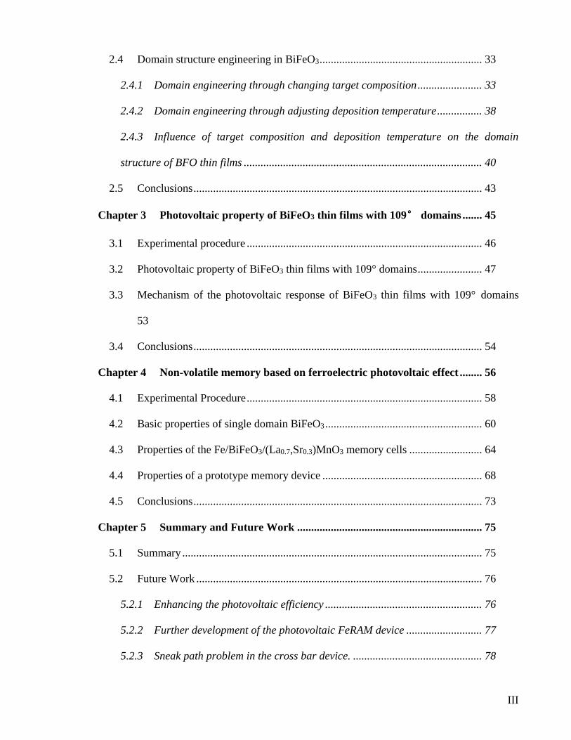
TABLE OF CONTENTS
ACKOWLEGEMENT .................................................................................................... I
TABLE OF CONTENTS .............................................................................................. II
LIST OF FIGURES ...................................................................................................... IV
LIST OF TABLES ...................................................................................................... VII
ABSTRACT. ............................................................................................................... VIII
Chapter 1 Introduction ............................................................................................... 1
1.1 Conventional and ferroelectric photovoltaic effect ............................................. 1
1.2 Previous work on BiFeO3 ................................................................................... 4
1.2.1 Physical Properties of Multiferroic BiFeO3 ................................................. 4
1.2.1.1 Crystal structure of BiFeO3 ............................................................................. 4
1.2.1.2 Ferroelectricity of BiFeO3 ............................................................................... 5
1.2.1.3 Magnetic property of BiFeO3 .......................................................................... 6
1.2.1.4 Ferroelectric domain structure of BiFeO3....................................................... 8
1.2.2 Domain wall functionalities and the control of domain structures in BiFeO3 thin
films 12
1.2.3 The mechanism of photovoltaic effect in BiFeO3 thin films ........................ 14
1.3 Purpose of Research .......................................................................................... 17
Chapter 2 Control the domain structure in BiFeO3 thin films ............................. 19
2.1 Introduction to film growth and characterization techniques used ................... 19
2.1.1 Pulsed laser deposition ............................................................................... 19
2.1.2 Domain structure characterization by piezoelectric force microscopy ...... 21
2.2 Thin film preparation and characterization procedure ...................................... 25
2.3 Optimization of BiFeO3 thin film growth parameters ...................................... 27
III
2.4 Domain structure engineering in BiFeO3 .......................................................... 33
2.4.1 Domain engineering through changing target composition ....................... 33
2.4.2 Domain engineering through adjusting deposition temperature ................ 38
2.4.3 Influence of target composition and deposition temperature on the domain
structure of BFO thin films ..................................................................................... 40
2.5 Conclusions ....................................................................................................... 43
Chapter 3 Photovoltaic property of BiFeO3 thin films with 109° domains ....... 45
3.1 Experimental procedure .................................................................................... 46
3.2 Photovoltaic property of BiFeO3 thin films with 109° domains ....................... 47
3.3 Mechanism of the photovoltaic response of BiFeO3 thin films with 109° domains
53
3.4 Conclusions ....................................................................................................... 54
Chapter 4 Non-volatile memory based on ferroelectric photovoltaic effect ........ 56
4.1 Experimental Procedure .................................................................................... 58
4.2 Basic properties of single domain BiFeO3 ........................................................ 60
4.3 Properties of the Fe/BiFeO3/(La0.7,Sr0.3)MnO3 memory cells .......................... 64
4.4 Properties of a prototype memory device ......................................................... 68
4.5 Conclusions ....................................................................................................... 73
Chapter 5 Summary and Future Work .................................................................. 75
5.1 Summary ........................................................................................................... 75
5.2 Future Work ...................................................................................................... 76
5.2.1 Enhancing the photovoltaic efficiency ........................................................ 76
5.2.2 Further development of the photovoltaic FeRAM device ........................... 77
5.2.3 Sneak path problem in the cross bar device. .............................................. 78

IV
LIST OF FIGURES
Figure 1.1 Working mechanism of a p-n junction solar cell. The built-in electric field which
exists in the interfacial area separates the electron-hole pairs generated under illumination. .. 1
Figure 1.2 Schematic of photovoltaic mechanism in ferroelectric thin film. Figure adapted
from [16]. (a) The upward polarization with downward built-in electric field and (b) the
downward polarization with upward built-in electric field. ...................................................... 3
Figure 1.3 (a)-(c) Crystal structure of (001) BFO viewing from different directions. Figure
adapted from [28]. ..................................................................................................................... 5
Figure 1.4 Ferroelectric hysteresis loops of epitaxial BFO films with different
crystallographic orientations. Figure adapted from [34]. .......................................................... 6
Figure 1.5 Magnetic structure of BFO. Figure adapted from [37]. ........................................... 8
Figure 1.6 Schematic of the four structural variants and corresponding eight polarization
variants in BFO thin film. ......................................................................................................... 9
Figure 1.7 Schematic of (a) 71° and (b) 109° domain patterns in BFO thin films. .................. 9
Figure 1.8 (a) Schematic of 71° domain walls (four domains with 3 domain walls). (b)
Corresponding band diagram across these domains and domain walls in dark. (i) demonstrates
light hitting the bulk domain and (ii) demonstrates light hitting the domain wall area. (c)
Evolution of band diagram under light illumination. (d) Detailed picture of the separation of
electron-hole pairs at the domain wall. Figure adapted from [3]. ........................................... 16
Figure 2.1 Schematic illustration of a pulsed laser deposition system. The inset shows the
plume during deposition. Figure adapted from [82]. .............................................................. 20
Figure 2.2 Schematic of the working mechanism of PFM. .................................................... 22
Figure 2.3 (a) The deflected laser hits the center of the photodiode when the cantilever is
undeflected. (b) How the laser spot shifts when an electric field is applied to a sample with
downward polarization. (c) How the laser spot shifts when the same electric field is applied to
a sample with upward polarization. ........................................................................................ 23
Figure 2.4 (a) The color code of IP PFM images. (b) The color code of OOP PFM images. The
cantilever of the AFM probe is long the [-110] direction of the sample. ............................... 25
Figure 2.5 PFM images of BFO thin films on exact STO substrate grown by (a) stoichiometric
BFO target and (b) B0.8FO target. ........................................................................................... 28
Figure 2.6 Topography and PFM images of BFO thin film grown at 680 ºC, using B0.8FO
target, under oxygen pressure of (a) 300 mtorr, (b) 200 mtorr, (c) 100 mtorr, and (d) 50 mtorr.
................................................................................................................................................. 30

V
Figure 2.7 Topography and PFM images of BFO thin films on GSO substrates deposited using
B0.8FO target at 680 °C, with the laser energy density of (a) 1.5 J/cm2, (b) 1 J/cm2, (c) 0.5 J/cm2,
and (d) 0.4 J/cm2. Left: topography, Middle: IP domain image, Right: OOP domain image. 32
Figure 2.8 Schematic of the growth of BFO thin film on miscut STO substrate (2º miscut along
[100] direction), and the structural variant selection. α is the rhombohedral distortion angle.
................................................................................................................................................. 33
Figure 2.9 Topography, IP and OOP PFM images of BFO thin film (grown by B0.8FO target)
on 2º miscut STO substrate. .................................................................................................... 33
Figure 2.10 Topography and PFM images of BFO thin films on GSO substrates deposited
using (a) B0.8FO, (b) B0.6FO, (c) B0.5FO, and (d) B0.4FO targets. ........................................... 35
Figure 2.11 PFM images of the same area with cantilever (a) along the [1-10] direction and (b)
along the [110] direction. ........................................................................................................ 37
Figure 2.12 Topography and PFM images of BFO thin films on GSO substrates deposited
using B0.8FO target at (a) 680 °C, (b) 700 °C, (c) 720 °C, and (d) 750 °C. ............................ 39
Figure 2.13 XRD patterns of films deposited (a) using targets with different composition, and
(b) at different substrate temperatures. ................................................................................... 40
Figure 2.14 The change of the downward pointing domain regions of BFO thin film with (a) Bi
content in the target and (b) deposition temperature............................................................... 41
Figure 2.15 Bi content in BFO thin films with 71° and 109° domains measured using EPMA.
................................................................................................................................................. 42
Figure 3.1 (a) Topography, (b) IP, (c) OOP PFM images of 109° BFO thin films on a normal
DSO substrate. (d) and (e) Schematic of polarization variants in the sample. (f) Topography,
(g) IP, and (h) OOP PFM images of 109° BFO thin films on a 2º miscut DSO substrate. The
arrow in (f) shows the miscut direction, and the arrow in (g) shows the net IP polarization
direction. ................................................................................................................................. 48
Figure 3.2 Schematic of the planar Pt electrodes on BFO thin film and the demonstration of
electrical connection. .............................................................................................................. 49
Figure 3.3 Photovoltaic property of BFO sample with mainly two polarization variants of 109°
domains. (a) I-V curves of the as-grown sample and the sample applied by different voltages.
(b) IP PFM image of as-prepared sample. (c)-(g) IP PFM images of the sample applied by
different voltages. The arrows show the net IP directions. ..................................................... 50
Figure 3.4 (a) Schematic of the polarization switching of 109° domains in BFO thin films. (b)
Schematic of the change of IP and OOP PFM images of the 109° stripe domains after
switching. ................................................................................................................................ 52
Figure 3.5 (a) Schematic of 109 domains, the circle demonstrates where the electrostatic
energy is high. (b) Schematic of vortex domains. Figure captured from [97]. ....................... 53

VI
Figure 4.1 Experimental setup for the electrical characterizations of the individual capacitors.
LSMO and Pt/Fe are used as the bottom and top electrodes in both cases. A four-probe
micromanipulator is used to connect the device to a commercial ferroelectric tester and
PicoAmp meter/DC voltage source for P-V and I-V characterizations. .................................. 59
Figure 4.2 Transmittance of the Pt/Fe electrode at different wavelength measured by using
UV-Vis spectroscopy. ............................................................................................................. 59
Figure 4.3 Basic properties of the STO substrate and single domain BFO films. (a) Schematic
of the miscut STO substrate and corresponding BFO growth, (b) 3-D topography of the BFO
film, (c) OOP PFM image of single-domain BFO film after switching the central 2 × 2 µm2
area, the inset shows the polarization switching path, (d) corresponding IP PFM image and
cantilever orientation during scan. .......................................................................................... 60
Figure 4.4 (a) typical P-V loop of the Fe/BFO/LSMO capacitor (red line is the corresponding
I-V curve), and (b) I-V curves of the Fe/BFO/LSMO capacitor under dark and light with
opposite polarization directions. ............................................................................................. 61
Figure 4.5 P-V loops measured at different frequencies. ........................................................ 62
Figure 4.6 Photovoltaic property of the Fe/BFO/LSMO device. Current-voltage curves
measured under different light intensity for (a) polarization down and (b) up states. (c) Open
circuit voltage and (d) short circuit current as functions of light intensity for both polarization
directions. ................................................................................................................................ 64
Figure 4.7 Influence of poling pulse width on (a) Voc, and (b) Isc of the capacitors. The
switching voltage changes from ± 3 V to ± 6 V. .................................................................... 65
Figure 4.8 Retention and fatigue behavior of the Fe/BFO/LSMO memory cell. (a) Open circuit
voltage and (b) short circuit current for both polarization directions show negligible change
after 4 months. (c) Polarization-voltage loops and (d) Current-voltage curves measured after
repetitive switching by pulses of ±3 V, 1 ms reveal no fatigue after 108 cycles. (e) Open-circuit
voltage and (f) Short-circuit show slight change after the switching cycles of 108. In (a,b,d,e,f),
blue: under light with polarization up; red: under light with polarization down. ................... 67
Figure 4.9 Schematic of the cross bar device structure and the demonstration of the electrical
connection. .............................................................................................................................. 69
Figure 4.10 Performance of a prototype 16 cell memory based on the cross bar architecture. (a)
Topography of the device with preset polarization direction indicated. Blue: polarization up,
Red: polarization down. (b) Open circuit voltages of all 16 cells indicated. These are measured
under 20 mW/cm2 light. Blue: positive photovoltage, Red: negative photovoltage. .............. 69
Figure 4.11 Retention and fatigue behavior of the 4 × 4 cross bar memory cell. (a) Open circuit
voltage and (b) short circuit current for both polarization directions show negligible change
after 2 months. (c) Polarization-Electric field loops and (d) Current-voltage curves measured
after repetitive switching by pulses of ±3 V, 1 ms reveal no fatigue after 107 cycles. (e)
Open-circuit voltage and (f) Short-circuit current show little change after 107 cycles. It is also
well known in the ferroelectric community that fatigue can be mitigated by using oxide
electrodes, suggesting that the non-volatile memory can sustain much more read/write cycles

VII
than Flash memory. In (a,b,d,e,f), blue: under light with polarization up; red: under light with
polarization down. ................................................................................................................... 70
LIST OF TABLES
Table 2.1 Structure, lattice parameter, thermal expansion coefficient of substrate and in plane
misfit strains of BFO on different substrates. ......................................................................... 26
Table 2.2 Deposition parameters used in this study. .............................................................. 27
Table 4.1 Comparison between different memory technologies.[108] ................................... 72

VIII
ABSTRACT
In conventional junction-based photovoltaic cells, the photovoltage is usually smaller than
the semiconductor band gap, due to the limitation of the energy barrier at the interface.
Contrarily, ferroelectric photovoltaic effect is a bulk effect of which the photovoltage is not
limited by the energy barrier. Therefore, ferroelectric photovoltaic effect has attracted much
research attention due to its wide potential applications. BiFeO3, a multiferroic material with
robust ferroelectric and magnetic orders at room temperature[1] and a band gap within visible
light range[2], provides a unique opportunity for bulk photovoltaic effect study. Earlier work
on BiFeO3 photovoltaic property attributed the effect mainly to the ferroelectric polarization.
However, a very large photovoltage was reported later in BiFeO3 films with regular 71°
domains.[3] The authors proposed that the effect arises from the electrostatic potential steps
at the domain walls. Moreover, BiFeO3 films with regular 109° domain walls are expected to
generate a significantly larger photovoltage, since the potential step at 109° domain walls
was reported to be much larger than that at 71° domain walls.[4] This project thus aimed to
study the photovoltaic effect of BiFeO3 films with regular 109° domains, in order to clarify
its correlation with the domain wall. To achieve this, we set our goal to control the domain
structure of BiFeO3 thin films first. In fact, the ability to control domain structure is an
essential work for various research topics. Ferroelectric domain walls in BiFeO3 have been
shown to possess unique properties that do not exist in bulk material. Theoretical studies
have predicted that a net electric field or magnetic moment could in principle exist in the
center of domain walls while the domain themselves were non-electric or non-magnetic.
However, a systematic investigation requires the precise control of domain structures in
BiFeO3, which is still lacking. In this project the underlying mechanism of domain
engineering will be addressed. Then, the photovoltaic effect of BiFeO3 films with regular
109° domains will be studied. The correlation of the photovoltaic effect with the domain
walls will be discussed. Finally, after this, we studied the application of the photovoltaic
effect of BiFeO3 films in memory device. The photovoltaic effect could be used to read the
polarization status of BiFeO3 films non-destructively. The properties of the memory cells
were studied and compared with other technologies.

IX
Pulsed Laser Deposition technique was used to grow BiFeO3 films. By using BiFeO3 target
with different Bi content or adjusting the deposition parameters, films with regular 71° to
109° domains can be obtained. The domain structure was tested by Piezoelectric Force
Microscopy, and the thin film composition was measured using Electron Probe X-ray
Micro-analyzer. It is revealed that decreasing Bi content in the target or increasing substrate
temperature changes the domain structure of BiFeO3 from 71° to 109°. Domain structure is
related to the Bi vacancies in the thin film. We suggest that a combination of interface effect
and defect induced internal field causes this evolution.
After the successful control of domain structure in BiFeO3 thin films, the photovoltaic
property of BiFeO3 thin films with 109° domains was studied. BiFeO3 thin films that contain
regular 109° domains with mainly two polarization variants were prepared by using miscut
DyScO3 substrates. A direct correlation between the 109° domains switching and the
photovoltaic response of the films was established, by conducting piezoelectric force
microscopy study using a planar device. The polarity of the photovoltage is switchable upon
polarization reversal. Besides, the photovoltage was also obtained in single domain BiFeO3
thin films. The results suggest that theoretical study might have overestimated the
contribution of domain walls to BiFeO3 photovoltaic effect.
After the study of the photovoltaic effect of BiFeO3 thin films, we investigated the possibility
of using ferroelectric photovoltaic effect in non-volatile memory. Capacitors of Fe/BiFeO3
/(La0.7,Sr0.3)MnO3 were prepared on miscut SrTiO3 substrates. Photovoltage and photocurrent
with opposite signs were obtained upon switching the polarization of the capacitor. The
stored polarization information in BiFeO3 could be read non-destructively by sensing the
photovoltage or photocurrent. The memory performance such as write energy, operation
speed, retention time and fatigue cycles compare favorably with other memories, such as
hard disk drive, flash memory, magnetoresistive random access memory and resistive
switching random access memory.

1
Chapter 1 Introduction
1.1 Conventional and ferroelectric photovoltaic effect
Conventional photovoltaic cells are based on p-n or Schottky junctions. Under
illumination, photons with energy higher than the semiconductor band gap are absorbed
to generate electron-hole pairs, which are then separated by the internal field. The internal
electric field is generated by the band bending which spans over a micrometer-thick
depletion region. Consequently, the photovoltage is limited by the energy barrier height at
the interface region and is always smaller than the semiconductor band gap.[5, 6] Figure
1.1 shows the working mechanism of a p-n junction photovoltaic cell.
Figure 1.1 Working mechanism of a p-n junction solar cell. The built-in electric field
which exists in the interfacial area separates the electron-hole pairs generated under
illumination.

2
Besides the conventional p-n or Schottky junctions, there are other pathways to achieve
charge separation in materials. For example, steady-state photocurrent has been observed
in homogeneous ferroelectric materials under illumination, which is named ferroelectric
photovoltaic effect. Since its discovery in BaTiO3 in 1956,[7] much research has been
done on this topic. Although the physical mechanism of photovoltaic effect in
ferroelectrics has not been fully clarified, it is certainly related to the ferroelectric
polarization.[8-14] Different from the internal field in conventional junction-based
photovoltaic cells, the polarization induced internal field extends over the whole
ferroelectrics. Therefore, ferroelectric photovoltaic effect is mainly a bulk effect.
Abnormally large photovoltage has been reported. For example, a large photovoltage of 7
V was reported for Pb0.97La0.03(Zr0.52Ti0.48)O3 ferroelectric thin film with planar structure
under ultraviolet light illumination.[11] Figure 1.2 shows the possible mechanism of
ferroelectric photovoltaic effect. The switchable photovoltaic effect was explained by the
polarization dependent band modification of the BiFeO3 (BFO) capacitor. The unscreened
polarization charge bends the electronic band and thus generates the built-in electric field
of which the direction depends on the polarization direction. When incident light energy
is above the band gap of the material, electron-hole pairs will be generated and then be
separated by the built-in electric field. For ferroelectric photovoltaic effect, besides the
polarization-induced internal field, other factor such as the Schottky barriers at the
interfaces between the ferroelectric material and the electrodes should also be taken into
consideration. The Schottky barrier also generates an internal field, which will contribute
to the photovoltaic effect.[9, 10, 15] For the sandwiched structure, the Schottky barriers at
the two ferroelectric-electrode interfaces are usually different even with the same

3
electrodes due to different processing conditions. It adds a non-switchable internal field to
the overall response. Therefore, the I-V curves with opposite polarization states under
light illumination are not symmetric.[9]
Figure 1.2 Schematic of photovoltaic mechanism in ferroelectric thin film. Figure adapted
from [16]. (a) The upward polarization with downward built-in electric field and (b) the
downward polarization with upward built-in electric field.
Ferroelectric photovoltaic effect has attracted much attention because of its potential
applications for optical detection[17], wireless actuation in microelectromechanical
systems (MEMS)[18, 19], optical information storage[20], and photovoltaic devices[21].
Previous studies mainly focused on BaTiO3 and Pb(ZrTi)O3, whose band gaps are in the
UV region. BFO, a multiferroic material with robust ferroelectric and magnetic orders at
room temperature[1] and a band gap (~ 2.7 eV) within visible light range[2], provides a
unique opportunity for ferroelectric photovoltaic effect study and applications.

4
1.2 Previous work on BiFeO3
Up to now, BFO is the only known single phase material with robust ferroelectric (Curie
temperature ~1103 K)[22] and magnetic (Neél temperature ~643 K)[23] orders coexisting
at room temperature. Furthermore, it is environmentally friendly and has a relatively
simple perovskite structure. Therefore, it has been intensively studied both experimentally
and theoretically.
1.2.1 Physical Properties of Multiferroic BiFeO3
1.2.1.1 Crystal structure of BiFeO3
At room temperature, BFO has a rhombohedral (point group R3c) structure.[24] Its
crystal structure is characterized by two highly distorted perovskite units connected along
their body diagonal direction, denoted as pseudocubic <111> pc [25], as shown in figure
1.3. At room temperature, the pseudocubic unit cell has a lattice parameter (αrh) of 3.965
Å, and a rhombohedral angle of ca. 89.3-89.4º.[24] The large displacement of the Bi ions
relative to the FeO6 octahedra gives rise to a large spontaneous polarization along the
<111>pc direction.[26, 27] As a result, there are totally eight possible polarization
directions which correspond to four structural variants.
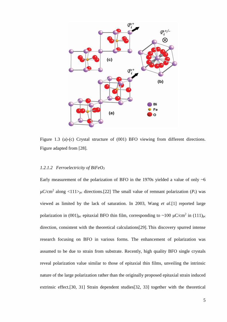
5
Figure 1.3 (a)-(c) Crystal structure of (001) BFO viewing from different directions.
Figure adapted from [28].
1.2.1.2 Ferroelectricity of BiFeO3
Early measurement of the polarization of BFO in the 1970s yielded a value of only ~6
μC/cm2 along <111>pc directions.[22] The small value of remnant polarization (Pr) was
viewed as limited by the lack of saturation. In 2003, Wang et al.[1] reported large
polarization in (001)pc epitaxial BFO thin film, corresponding to ~100 μC/cm2 in (111)pc
direction, consistent with the theoretical calculations[29]. This discovery spurred intense
research focusing on BFO in various forms. The enhancement of polarization was
assumed to be due to strain from substrate. Recently, high quality BFO single crystals
reveal polarization value similar to those of epitaxial thin films, unveiling the intrinsic
nature of the large polarization rather than the originally proposed epitaxial strain induced
extrinsic effect.[30, 31] Strain dependent studies[32, 33] together with the theoretical

6
calculation[29] also suggest that the intrinsic polarization of BFO epitaxial films is
actually insensitive to strain. Ferroelectric hysteresis loops of epitaxial BFO films with
different crystallographic orientations are shown in figure 1.4. The remnant polarization
of BFO thin film on (100) substrate is around 65 µC/cm2, which reaches 100 µC/cm2
when grown on (111) oriented substrate.
Figure 1.4 Ferroelectric hysteresis loops of epitaxial BFO films with different
crystallographic orientations. Figure adapted from [34].
1.2.1.3 Magnetic property of BiFeO3
BFO has a G-type antiferromagnetic structure. As shown in figure 1.5, each Fe3+
magnetic moment is surrounded by six antiparallel moments of the nearest Fe3+
neighbors. In another word, the Fe3+ magnetic moments are coupled ferromagnetically
within the pseudocubic (111)pc planes and antiferromagnetically between adjacent planes.

7
In bulk BFO, the orientation of the antiferromagnetic vector follows a cycloidal spiral
with a long period of 620 ± 20 Å, where [110]pc is the spiral direction and (110)pc is the
spin rotation plane.[35, 36] Although there is canting of spins, the net magnetic moment
in bulk BFO is zero since it follows the spiral structure. For BFO thin films, there is no
spin cycloid due to symmetry breaking induced by epitaxial strain. BFO thin films thus
have a weak magnetic moment which is generated by the canting. The weak canting is
caused by the local magnetoelectric coupling,[37] which leads to a small net magnetic
moment. However, magnetization of BFO thin films caused by the small canting is very
small. A significant enhancement of the magnetization (~0.5 μB/Fe) was reported
originally by Wang et al.[1], and later study suggested that the enhanced magnetization
may be correlated with the valence change of Fe ions or magnetic second phases.[38, 39]
First principles calculations of the magnetocrystalline anisotropy energy show that the
preferred orientation of the individual magnetic moment is perpendicular to the
rhombohedral axis.[40] There is a six-fold degeneracy within the corresponding (111)pc
plane, resulting in an effective ‘easy magnetization plane’ for the magnetic moments. The
easy magnetization plane is always perpendicular to the ferroelectric polarization and
coupled to the ferroelectric/ferroelastic strain state. Consequently, ferroelectric
polarization switching by either 71º or 109º will change the orientation of the easy
magnetization plane.[41] The electric field control of magnetization at room temperature
through the coupling between multiferroic BFO and a ferromagnet CoFe was reported
recently,[42] making BFO an ideal candidate for future magnetoelectric random access
memory.[43]

8
Figure 1.5 Magnetic structure of BFO. Figure adapted from [37].
1.2.1.4 Ferroelectric domain structure of BiFeO3
In ferroelectrics, domain structures form to release the elastic/electrostatic energy at the
expense of increased interfacial energy at the domain boundaries.[44, 45] Bulk BFO has a
rhombohedral structure, and its polarization points along one of the body diagonal
directions. When BFO is epitaxially grown on substrates, the rhombohedral symmetry is
reduced to monoclinic with the distortion along <111>pc direction, due to the epitaxial
strain. Therefore, there are totally four ferroelastic structural variants which correspond to
eight polarization variants as shown in figure 1.6. These eight polarization variants can
form three types of domain walls (71º, 109º, and 180º) depending on the angles between
the adjacent polarization variants. For example, polarization P1+ and P2
+ form a 71º

9
domain wall, polarization P1+ and P2
- form a 109º domain wall, and polarization P1+ and
P1- form a 180º domain wall.
Figure 1.6 Schematic of the four structural variants and corresponding eight polarization
variants in BFO thin film.
Figure 1.7 Schematic of (a) 71° and (b) 109° domain patterns in BFO thin films.
Domain structures depend on the substrate, substrate orientation, and the deposition
parameters. Domain patterns in epitaxial BFO ferroelectric thin films could be predicted

10
according to the theory proposed by Streiffer et al. [45] For BFO thin films on the (001)
oriented substrates, the four structural variants are energetically degenerate, and therefore
have the equal chance to exist in the film. The combination of different polarization
variants can lead to complicate domain structures. Possible domain walls are decided by
both mechanical and charge compatibility. To satisfy the mechanical requirement, domain
patterns may form with either {100} or {101} boundaries (to release strain energy),
corresponding to 109º and 71º domain patterns, respectively. On the (001) substrate,
109º domain patterns have a puckered fashion on the topography, while 71ºdomain
patterns have a flat topography, as shown in figure 1.7. Charge compatibility must be
satisfied to achieve neutral charge at the domain boundaries. Therefore, 109º patterns
must have the opposite out-of-plane (OOP) component of polarization in adjacent
domains, while charge neutrality for 71º domains can only be obtained when all domains
have the same OOP component of polarization, as shown in figure 1.7. If we consider the
total net polarization of the film, the alternating OOP components of polarization in 109°
domain patterns will cancel each other out, and thus reduce the depolarization field; while
the same OOP components of polarization in 71ºdomain patterns lead to a finite
component in the substrate normal direction, corresponding to a fully-poled state. As a
consequence, the fully-poled state 71º domains have a large depolarization field in the
film which needs to be balanced to make the domains stable. To sum up, 71º domains
have {101} type domain walls with a flat topography on (001) surface, and all domains
have the same OOP polarization component, corresponding to fully-poled state; while
109ºdomains have {100} type domain walls with a puckered fashion of topography, and
the adjacent domains have opposite OOP polarization component, lending to no normal

11
component of the net polarization. And for the 180° domain walls, they don’t need to
follow any specific crystallographic planes, because 180º domains are ferroelectric rather
than ferroelastic, there is no elastic constraint on the domain wall.
For a BFO thin film grown on (001) oriented SrTiO3 (STO) substrate, individual domains
are energetically degenerate. So four structural variants have the equal chance to appear,
and twinning domain patterns are expected to form to release the elastic energy in the film.
However, experimentally, BFO films on STO substrates are in a fully poled state, only the
upward polarization variants are observed. Some studies suggest that it is due to the
oxygen vacancies.[46, 47] As for BFO thin films on (110) and (111) oriented substrates,
their domain patterns are relatively simple. For BFO thin films on (110) oriented STO
substrate, the compressive strain will drive the polarization towards the OOP direction,
and thus favors only two out of the four structural variants. For BFO films on (111) STO
substrates, under compressive strain, only the polarization variants perpendicular to the
film surface is energetically stable. Therefore, therefore the structural variants are further
reduced to one, corresponding to a single domain state.[34] The ferroelectric domain
structure can be revealed by using piezoelectric force microscopy (PFM), which will be
explained in details in chapter 2.
The dynamic polarization switching process has also been investigated using PFM. All
three possible switching mechanisms (namely 71°, 109° and 180° switching) have been
observed. The 71°, 109° switching are accompanied by the change of structure distortion,
thus being ferroelastic in nature, whereas 180° switching is purely ferroelectric. 180°

12
polarization reversal seems to be the most favorable switching mechanism in epitaxial
films under an applied field along [001]pc.[41]
1.2.2 Domain wall functionalities and the control of domain structures in BiFeO3 thin
films
Domain walls exist in many materials that possess certain order parameters such as
ferroelectric and ferromagnetic materials, superconductors, and liquid crystals. They are
formed when the symmetry of a single crystalline region is changed or reduced in the
process of a phase transition, and separate regions with different orientation of the order
parameter form. The response of a material to applied fields is defined by the static and
dynamic properties of the domain walls. This is very important in numerous technological
applications, such as nonvolatile ferromagnetic, ferroelectric memories,
magnetoresistance and spin-valve devices, etc.[48]
Domain wall represents a special type of inhomogeneity. Its symmetry is lowered
compared with that of the domain bulk. Large structural gradients in domain walls result
in new effects that do not exist in the domain bulk.[49, 50] The detailed structure and
formation energy of domain wall in conventional ferroelectrics are now well
established.[51-53] On the contrary, research on the domain walls in multiferroics is
scarce. Lajzerowicz predicted that domain walls in systems with two coupled order
parameters could result in the emergence of one order inside the domain wall of the
other.[54] For multiferroic materials, it means a net electric or magnetic moment could in
principle exist in the center of domain walls while the domain themselves were

13
non-electric or non-magnetic. Later, Privratska and Janovec[49, 50] generalized this
analysis to show what crystal symmetries might exhibit such behavior, using
group-theory argument. Multiferroic YMnO3 was studied and the results showed that the
antiferromagnetic walls strongly interact with ferroelectric walls.[48] Research on
multiferroic GdFeO3 demonstrated that ferroelectric polarization and magnetization can
be controlled by magnetic and electric field, respectively, which was attributed to the
unique feature of composite domain walls.[55] A linear correlation between the density of
ferroelastic domain walls and ferromagnetism has also been reported in thin films of
TbMnO3, suggesting that the ferroelastic domain walls in this antiferromagnetic material
may be ferromagnetic.[56, 57] Furthermore, the converse effect of polarization emerging
inside the domain walls of a magnet was demonstrated by Logginov et al.[58] Theoretical
research has also predicted that both the domain wall thickness and the domain width of
magnetoelectric multiferroics should be bigger than that of pure ferroelectrics and smaller
than that of pure ferromagnets.[59] Experimental study on multiferroic DyMnO3 verified
this conclusion.[60] Recently, several groups reported domain wall conductivity[61] and
magnetoelectricity[37, 62, 63] in BFO thin films.
Domain structure has significant effect on the properties of multiferroic BFO. It is thus
very important to control the domain structure for different applications. Many factors
affect the domain structure in BFO, and much research has been done on this topic. Zhang
et al.[64] suggested that both the elastic energy and depolarization energy play important
roles in determining the equilibrium domain structure in BFO. Varying film orientation
and strain states leads to different results. It has been demonstrated that thicker films

14
favor the formation of regular domain structures.[65, 66] Chu et al.[67] has reported that
for BFO films grown on DyScO3 (DSO) with SrRuO3 bottom electrode, the growth
mechanism of the underlying SrRuO3 layer determines the final domain structure of BFO.
SrRuO3 layers grown by step-flow and step-bunching mechanisms lead to domain
structures with 2- and 4-polarization variants, respectively. To reduce the domain variants,
a break in the degeneracy of the various polarization directions must be induced. One way
to achieve this is by using vicinal substrates. Furthermore, asymmetric boundary
conditions can lead to a preferred direction of the OOP component of the polarization. By
carefully controlling the boundary conditions, Chu et al.[68] have obtained BFO films
with only 71º domain walls located on (101) type planes and 109º domain walls located
on (100) type planes.
1.2.3 The mechanism of photovoltaic effect in BiFeO3 thin films
BFO has a narrow band gap (2.7 eV)[69] which is within the visible light range. The
visible-light photovoltaic effect makes BFO a promising candidate for novel photovoltaic
cells and optoelectronic devices.
In year 2003, a switchable visible-light photovoltaic effect in single domain BFO crystals
was reported by Choi et al.[70], which triggered researchers' interests on the study of the
photovoltaic effect in BFO. Normal ferroelectric photovoltaic effect in a single crystal
single domain BFO is caused by the incomplete screening of polarization charge, which
gives rise to the depolarization field in the sample. This depolarization field direction
depends on the polarization direction, and is thus switchable.[16, 71, 72] On top of the
15
depolarization field, the schottky barriers at the electrode/film interface, and the different
work functions of the electrodes may also induce band bending in the film, but these are
independent of the polarization direction.[73]
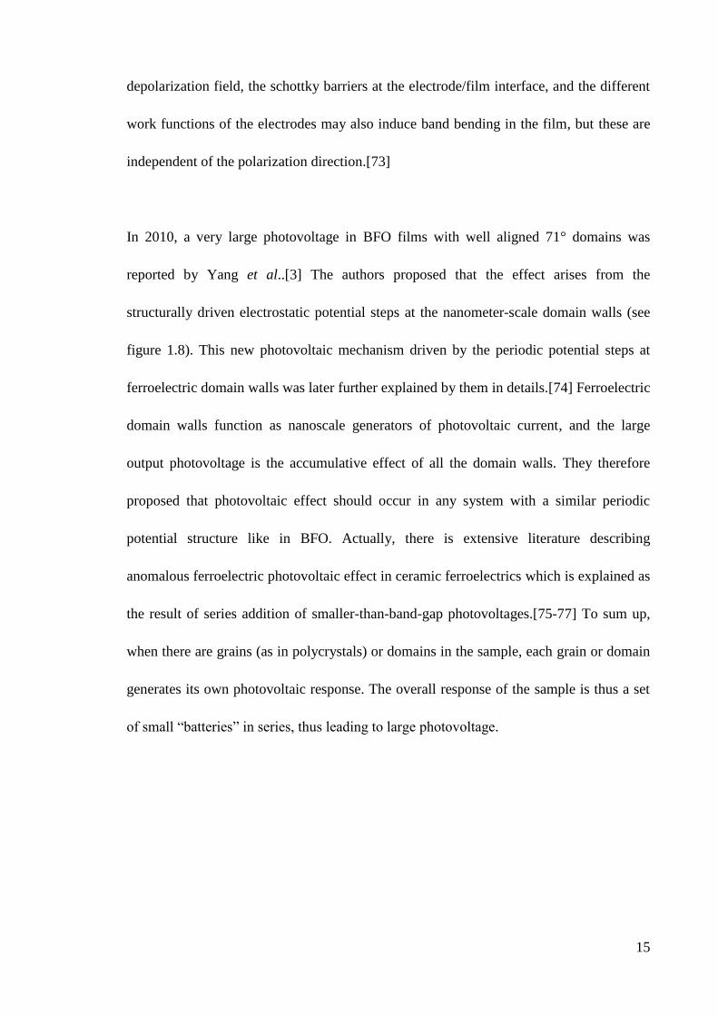
In 2010, a very large photovoltage in BFO films with well aligned 71° domains was
reported by Yang et al..[3] The authors proposed that the effect arises from the
structurally driven electrostatic potential steps at the nanometer-scale domain walls (see
figure 1.8). This new photovoltaic mechanism driven by the periodic potential steps at
ferroelectric domain walls was later further explained by them in details.[74] Ferroelectric
domain walls function as nanoscale generators of photovoltaic current, and the large
output photovoltage is the accumulative effect of all the domain walls. They therefore
proposed that photovoltaic effect should occur in any system with a similar periodic
potential structure like in BFO. Actually, there is extensive literature describing
anomalous ferroelectric photovoltaic effect in ceramic ferroelectrics which is explained as
the result of series addition of smaller-than-band-gap photovoltages.[75-77] To sum up,
when there are grains (as in polycrystals) or domains in the sample, each grain or domain
generates its own photovoltaic response. The overall response of the sample is thus a set
of small “batteries” in series, thus leading to large photovoltage.

16
Figure 1.8 (a) Schematic of 71° domain walls (four domains with 3 domain walls). (b)
Corresponding band diagram across these domains and domain walls in dark. (i)
demonstrates light hitting the bulk domain and (ii) demonstrates light hitting the domain
wall area. (c) Evolution of band diagram under light illumination. (d) Detailed picture of
the separation of electron-hole pairs at the domain wall. Figure adapted from [3].
For the domain wall contribution, it was reported that potential steps at different domain
walls are different, and the potential step at 109° domain walls is much larger than that at
71° domain walls.[61] It is thus expected that BFO films with well aligned 109º domain
walls will generate a significantly larger photovoltage. However, macroscopic
photovoltaic measurement of BFO films with 109º domain walls is restricted due to the
presence of domains with in-plane polarizations pointing in opposite directions, thus
canceling the effect. Inspired by this prediction, we therefore set our goals to study the
photovoltaic effect of BFO thin films with 109º domain walls to verify the theoretical
prediction of its significantly larger photovoltage. To reach our goal, we need to obtain
BFO thin films with 109º domains first. We therefore started our study by controlling the
domain structures in BFO films.

17
Since the photovoltaic response of BFO is switchable upon polarization reversal, it is
possible to use the photovoltaic response as a read-out signal for ferroelectric random
access memory (FeRAM). In conventional FeRAM, to read the information stored, a bias
is applied to the ferroelectric capacitor, and the polarization switching current is detected.
This process is destructive and a rewrite step is needed, which leads to high energy
consumption and reduced device lifetime. As a result, FeRAM takes up only a negligible
share of today’s memory market. To solve this problem, alternative non-destructive
read-out method is needed. Since the photovoltaic effect of ferroelectrics can be
switchable upon polarization reversal, the coupling of the photovoltaic effect and the
ferroelectric polarization can fulfill the non-destructive readout of the stored information
by simply sensing the photovoltage or photocurrent. So, after studying the photovoltaic
effect of BFO thin films, non-volatile memory device which is based on ferroelectric
photovoltaic effect will be investigated.
1.3 Purpose of Research
The objectives of this project are:
(i) To achieve precise control of the domain structures in BFO and understand the
mechanism behind it. This will be achieved by fine tuning the growth
parameters of the film, such as target composition, substrate temperature etc.
The domain structures will be studied using PFM and correlated to the
composition and structure of the film to identify the underlying mechanism.

18
(ii) To study the photovoltaic effect of BFO with 109º domains. It has been
suggested that the unusually large (above band gap) photovoltage observed in
BFO films with 71º domains is related to the energy band bending at the
domain walls.[78] Theoretical study has suggested that larger band bending
should occur at 109º domain walls, leading to higher photovoltage. However,
this prediction has not been tested experimentally. After achieving precise
control of the domain structure in BFO, we will investigate the photovoltaic
response of films with 109º domains to verify this prediction.
(iii) To explore the application of ferroelectric photovoltaic effect in non-volatile
memories. Even though large photovoltage has been observed in BFO films, it
is unlikely that ferroelectric materials can be used for solar energy harvesting.
This is mainly due to the intrinsic high resistivity of ferroelectric materials,
limiting the energy conversion efficiency. However, since the photovoltaic
response of ferroelectric materials depends on the polarization direction, it can
be used as the read-out signal for FeRAM. In this project, we also investigate
the prototype photovoltaic effect-based FeRAM and compare it performance
with other technologies under development.

19
Chapter 2 Control the domain structure in BiFeO3 thin films
In this chapter, we present our investigation on the influence of target composition and
deposition temperature on the domain structure in BFO.
2.1 Introduction to film growth and characterization techniques used
2.1.1 Pulsed laser deposition
Pulsed laser deposition (PLD) is a popular physical vapor deposition technique for
functional oxide thin films.[79-81] A schematic diagram of a basic PLD system is shown
in figure 2.1. The deposition chamber is equipped with target holder, substrate heater,
rotators, windows, and vacuum pumps. During the deposition process, a pulsed laser
beam is focused onto the target. When the laser energy density is above a threshold value,
the target materials (bulk ceramics or single crystals) will be evaporated, forming a
plasma plume. The plume travels normal to the target surface until it reaches the heated
substrate surface, and film growth occurs. During the film deposition, the chemical
environment in the chamber is controlled by various pressure gauges, and the temperature
is controlled by the heating system which is connected to the substrate holder. High
quality epitaxial films require laborious optimization of deposition parameters including
substrate temperature, oxygen pressure, laser energy density, target-to-substrate distance
etc. Moreover, different materials could have dramatically different growth windows
depending on the nature of the composition elements. Our PLD system uses a KrF
excimer laser with a wave length of 248 nm and a repetition rate from 1 to 20 Hz.

20
Figure 2.1 Schematic illustration of a pulsed laser deposition system. The inset shows the
plume during deposition. Figure adapted from [82].
PLD technique has many advantages. The laser energy density is very high, up to 1 to 5
J/cm2 at the target surface after focusing by the optical lens. The high energy laser ablates
the target material and preserves the complex stoichiometry of target material. It is thus
especially suitable for the deposition of films with complex compositions. Moreover,
multiple targets in the deposition chamber enable the deposition of super-lattices,
hetero-structures, and multi-layers by simply changing the targets.
The main disadvantage of PLD is that it can only grow films with very small size due to
the highly forward directional property of the plume. Typically, thin films with a uniform
thickness can only be obtained within a limited area, for example, 1-2 cm in diameter in
our case. Therefore, PLD can only be used in the research community, but not for

21
industrial production. Besides this, the overheated molten particulates from the target will
cause the “splashing” problem, in which case macroscopic particles will be produced.
2.1.2 Domain structure characterization by piezoelectric force microscopy
Piezoelectric force microscopy (PFM) is a variant of atomic force microscopy (AFM)
which can be used to observe and manipulate ferroelectric domains at nano-scale. It is
based on the converse piezoelectric effect. Since all ferroelectrics process piezoelectric
property, applying an electric field to the ferroelectric sample will result in the change of
its dimension. PFM is performed under contact scan mode, in which the cantilever of the
AFM probe is kept in contact with the sample surface under a constant force. To reveal
the polarization direction in the sample, a modulated alternative current (AC) bias V(ω) =
Vac cos (ωt) of frequency ω and amplitude Vac is applied to the AFM tip. The AC bias will
generate an oscillating deformation of the sample surface, d = d0 + D cos(ωt + φ), where
d0 is the equilibrium position, D is the amplitude, and φ is the phase difference with the
driving field. The resulting movement of the cantilever is detected by the photodiode,
through which the oscillating surface displacement is converted into an oscillating voltage.
A lock-in-amplifier is then used to retrieve the amplitude (D) and phase (φ) of the sample
surface deformation which is induced by converse piezoresponse effect. The amplitude
signal gives information about the magnitude of the piezoelectric coefficient, while the
phase signal determines the polarization direction. Figure 2.2 shows schematically working
mechanism of PFM.

22
Figure 2.2 Schematic of the working mechanism of PFM.
Direction of the cantilever deflection depends on the mutual orientations of the electric
field and polarization. For the upward domains (polarization vector oriented normal to the
sample surface), applying a positive bias to the tip results in the shrinkage of the sample,
and the sample surface oscillation is out of phase with respect to the applied AC voltage,
φ = 180º. On the contrary, for downward domains, the positive bias will cause the sample
to expand, and the surface oscillation is in phase with respect to the applied voltage, φ=0º.
Consequently, domains with different polarization orientations will show contrasts in the
PFM phase images, as shown in figure 2.3. The red line indicates the laser beam, and the
panel is the photodiode which has A, B, C, D, four quadrants. Figure 2.3 (a) shows the

23
original state when the cantilever is undeflected, and (b) and (c) show how light spot
moves when a bias is applied to the samples with oppositely oriented domains.
Figure 2.3 (a) The deflected laser hits the center of the photodiode when the cantilever is
undeflected. (b) How the laser spot shifts when an electric field is applied to a sample
with downward polarization. (c) How the laser spot shifts when the same electric field is
applied to a sample with upward polarization.
Detecting the vertical deformation of the sample reveals the OOP polarization direction.
This is referred to as vertical PFM. For BFO, vertical PFM alone is not enough to
determine the local polarization direction since it is along the body diagonals. Later PFM
detects the torsion of the cantilever caused by the lateral displacement of the sample
surface. If the polarization vector is perpendicular to the electric field, a shear strain will
be generated under tip bias. The shear stain leads to the angular torsion of the cantilever
which can be detected by the photodiode detector.

24
Figure 2.3 shows schematically how the vertical and lateral deflections are detected. The
photodetector is divided into four quadrants. Vertical signal = (VA+VB) - (VC+VD), and
lateral signal = (VA+Vc) - (Vb+VD).
The vertical and lateral PFM give rise to OOP and in-plane (IP) domain images,
respectively, through which the OOP and IP polarization component could be determined.
By combining the two PFM images, three-dimensional polarization vectors can be
reconstructed to reveal the exact ferroelectric domain configurations in the sample.
In the case of (001)pc BFO films, the contrast of PFM images can be interpreted as below.
The cantilever of the AFM probe is along the <110>pc direction of the film, as shown in
figure 2.4. The up and down components of the polarization should give rise to opposite
contrast (yellow and purple, respectively, in our system) in the OOP PFM image, because
their OOP piezoresponses are opposite with respect to the driving force. Domains with
polarization IP components along the cantilever direction (P2- and P4
- in figure 2.4 (a)) do
not give rise to IP PFM signal (zero amplitude), because they bend the AFM cantilever
along its length which cannot be detected by the system. A medium contrast (brown color
in our system) will be generated in the IP PFM images. Domains with polarization IP
component pointing to the right with respect to the cantilever direction (P3- in figure 2.4
(a)) should produce an opposite tone as compared with domains having polarization IP
component pointing to the left (P1- in figure 2.4 (a)). They will generate two opposite
contrasts (yellow and purple) in the PFM images, respectively. By analyzing the contrasts

25
of the IP and OOP PFM images, we can therefore reconstruct the domain structure in
BFO thin film.
Figure 2.4 (a) The color code of IP PFM images. (b) The color code of OOP PFM images.
The cantilever of the AFM probe is long the [-110] direction of the sample.
2.2 Thin film preparation and characterization procedure
Epitaxial BFO thin films are deposited on STO (001), and GdScO3 (110)o (GSO, the
subscript o refers to orthorhombic structure) single crystal substrates. The Structure,
lattice parameter, thermal expansion coefficient of substrate and in plane misfit strains of
BFO on different substrates are listed in table 2.1. BixFeO3 (BxFO) targets (KJMT
corporation) with x = 1, 0.8, 0.6, 0.5, 0.4 are used. The densities of the targets are 6.2
g/cm3, 7.2 g/cm3, 5.4 g/cm3, 4.4 g/cm3, and 4.0 g/cm3, respectively. The difference in
target density does not affect the film growth rate or growth mode under optimized
condition.

26
Table 2.1 Structure, lattice parameter, thermal expansion coefficient of substrate and in
plane misfit strains of BFO on different substrates.
Material Structure Lattice parameter(Å)
a b c
Thermal expansion
coefficient (10-6 K-1)
Misfit
strain
BFO Rhombohedral 3.965 3.965 3.965 6.5~13 /
STO Cubic 3.905 3.905 3.905 10.4 -1.4%
GSO Orthorhombic 5.49 5.75 7.93 10.9 0.2%
(i) Substrate and target preparation.
The substrate is ultrasonically cleaned for ten minutes in acetone and ethanol successively
to remove the residuals on the surface due to polishing. The target surface should be
polished with fine sand paper before deposition in order to remove the laser burned layer
formed during previous deposition, which may have different composition.
(ii) Film deposition.
After cleaning, the target and substrate are placed into the deposition chamber, which will
then be pumped to a base pressure of <10-5 Torr. The target-substrate distance is ~6 cm.
Then, the pumping valve is closed with a small leak left and the oxygen flow rate is
adjusted to maintain a desired dynamic pressure during substrate heating. The substrate
temperature is raised to desired value at a heating rate of 20 °C/min. Before the deposition,
laser energy and frequency are adjusted to the desired values. KrF excimer laser with 248
nm wavelength is used in the deposition. The laser energy is around 1 J/cm2. When the
temperature of the substrate is ready, the laser is turned on and film deposition occurs.
Details of the primary deposition parameters are listed in table 2.2.

27
Table 2.2 Deposition parameters used in this study.
Target Substrate
temperature
O2
partial pressure
Energy
density
Laser
frequency
Target-substrate
distance
BixFeO3, x=0.4,
0.5,0.6,0.8 and 1 680-750ºC 100mTorr ~1J/cm2 5Hz 6 cm
(iii) Post-deposition annealing in oxygen.
When deposition is finished, the valve leak is closed and oxygen is introduced into the
chamber till ambient pressure while the substrate remains at its deposition temperature. It
is then cooled down to room temperature at a rate of 5 °C/min.
(iv) Characterization of thin films
The domain structures are obtained using PFM (Asylum Research MFP-3D) with Pt/Ti
coated tips. JXA-8530F Field Emission Gun Electron Probe X-ray Micro-analyzer
(FEG-EPMA) is used to check the film composition. X-ray diffraction (XRD)
measurements are performed using a Shimadzu XRD6000 x-ray diffractometer.
2.3 Optimization of BiFeO3 thin film growth parameters
During film deposition by PLD, the thermodynamic environment for the phase formation
and stabilization is mainly determined by the growth temperature and oxygen pressure,
which are therefore the most important growth parameters. We have mapped out the
growth window for pure phase BFO thin film previously [83]. The deposition temperature
and oxygen pressure can be varied from 600 ºC to 750 ºC, and 1 mTorr to 300 mTorr,

28
respectively. Lower deposition temperature and higher oxygen pressure can result in the
formation of Bi2O3, while Fe2O3 will form under the opposite growth conditions.[84, 85]
This phenomenon could be explained by the volatility of Bi element. During the
deposition, after Bi and Fe arrive at the substrate, Bi might re-evaporate due to its
volatility which is more prominent at higher temperature or lower pressure. Therefore
substrate temperature and oxygen pressure can affect the re-evaporation process of Bi,
and thus adjust the Bi/Fe ratio. Under proper temperature and pressure, Bi/Fe ratio will be
close to 1. Similar results were also reported by Béa et al.[84]
Figure 2.5 PFM images of BFO thin films on exact STO substrate grown by (a)
stoichiometric BFO target and (b) B0.8FO target.
We started our study by using a stoichiometric BFO target and (001) STO substrate. At a
substrate temperature of 680 °C, the BFO films deposited using stoichiomitric target

29
contains a small amount of Bi2O3 secondary phase, and the domains are mosaic as shown
in figure 2.5 (a). By reducing the Bi content in the target to 0.8, the secondary phase is
eliminated and regular stripe domains are obtained as shown in figure 2.5 (b). This is
contradictory to common belief that extra Bi is needed in the target to compensate its high
volatility. However, we suggest that the high volatility of Bi has two competing effects:
(1) more Bi being evaporated from the target than Fe during laser ablation; and (2) high
possibility of Bi escaping from the substrate surface. So the film composition doesn’t not
depend on the target alone, and other deposition parameter such as substrate temperature
is also very important.

30
Figure 2.6 Topography and PFM images of BFO thin film grown at 680 ºC, using
B0.8FO target, under oxygen pressure of (a) 300 mtorr, (b) 200 mtorr, (c) 100 mtorr, and
(d) 50 mtorr.
Figure 2.6 shows the topography and PFM images of BFO thin films grown under
different oxygen pressures within the deposition window. B0.8FO target is used, and the
deposition temperature is 680 ºC. We can see that best quality BFO thin film with

31
smooth topography and regular stripes is obtained under 100 mtorr oxygen pressure. The
topography becomes rougher with more particles with the increase of the oxygen pressure.
On the other hand, BFO thin film starts to decompose when the oxygen pressure
decreases to 50 mtorr. We can see from figure 2.6 (d) that, there are holes in the film, and
the stripe domains start to disappear. We therefore fixed the oxygen pressure at 100 mtorr
in this study.

32
Figure 2.7 Topography and PFM images of BFO thin films on GSO substrates deposited
using B0.8FO target at 680 °C, with the laser energy density of (a) 1.5 J/cm2, (b) 1 J/cm2,
(c) 0.5 J/cm2, and (d) 0.4 J/cm2. Left: topography, Middle: IP domain image, Right: OOP
domain image.
The laser energy density has been varied from 0.4 J/cm2 to 1.5 J/cm2. As shown in figure
2.7, for films grown using B0.8FO target, smooth surface and regular domains were

33
obtained when the laser energy density is 1.0 J/cm2. At higher or lower energy density,
particles are observed on the sample surface and the domain structure becomes random.
We have fixed the laser energy density at 1 J/cm2.
2.4 Domain structure engineering in BiFeO3
2.4.1 Domain engineering through changing target composition
Figure 2.8 Schematic of the growth of BFO thin film on miscut STO substrate (2º miscut
along [100] direction), and the structural variant selection. α is the rhombohedral
distortion angle.
Figure 2.9 Topography, IP and OOP PFM images of BFO thin film (grown by B0.8FO
target) on 2º miscut STO substrate.

34
BFO thin films grown on STO contain all 4 upward polarization variants (figure 2.5 (b)).
This is expected because of the cubic symmetry of STO. A break in symmetry is
necessary to reduce the polarization variants. This can be realized by using miscut (along
(100) direction) substrate. The anisotropic surface states can reduce the 4 structural
variants of BFO film to 2, as shown in figure 2.8. The formation of structural variant r1
and r4 is prohibited on miscut STO substrate, because their rhombohedral distortion is
mechanically unfavorable. Indeed, the PFM images shown in figure 2.9 confirm the effect.
The film topography shows a step pattern. Stripe domains with 2 structural variants
separated by 71º domain walls are observed in the IP image. For films on miscut STO
substrate, the stress is easier to relax along the miscut direction than along the step
edges.[86] Therefore the energetically favorable distortion is along the downhill miscut
direction, which results in the stripe domains with only two structural variants.
Similar effect can be achieved by using substrates with lower symmetry, such as
orthorhombic DSO and GSO substrates. These substrates have a surface with non-square
unit cell, resulting in anisotropic stress in pseudocubic epitaxial films. The advantage of
using such substrates is that they can break the symmetry between different polarization
variants, but does not introduce topographic anisotropy that may complicate the result
analysis.
35
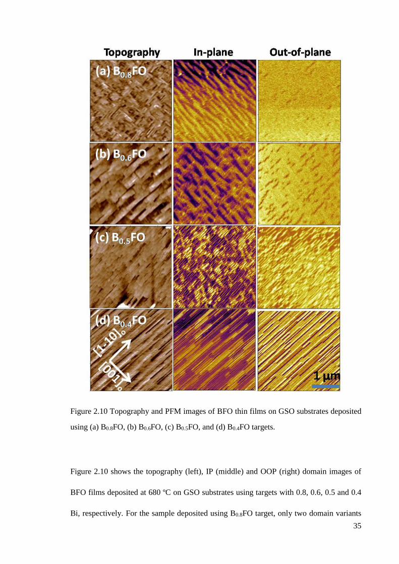
Figure 2.10 Topography and PFM images of BFO thin films on GSO substrates deposited
using (a) B0.8FO, (b) B0.6FO, (c) B0.5FO, and (d) B0.4FO targets.
Figure 2.10 shows the topography (left), IP (middle) and OOP (right) domain images of
BFO films deposited at 680 ºC on GSO substrates using targets with 0.8, 0.6, 0.5 and 0.4
Bi, respectively. For the sample deposited using B0.8FO target, only two domain variants

36
are observed in the IP image, consistent with early reports on the effect of anisotropic
substrates.[67, 87, 88] The OOP image shows uniform contrast, indicating that 71º
domains are obtained.[28] However, since the film is deposited on GSO substrate without
a bottom electrode, it is rather surprising to observe 71º domains, which are fully poled
along the OOP direction. There must be an internal bias in the as-deposited films that
competes with the large depolarization field. Possible origins of such internal field
include (1) interface bond reconstruction,[89, 90] (2) interface valence mismatch;[91] and
(3) defects, e.g. oxygen vacancies, accumulation at the interface.[92]
Interestingly, by reducing the Bi content in the target, we can change the domain structure
of the as-deposited film gradually. When B0.6FO target is used, the domains are still
mainly 71°, however, the quantity of pointing-down domains increases as shown by the
increasing dark regions in the OOP domain image in figure 2.10 (b), since dark contrast in
OOP PFM image means polarization pointing “down”. When B0.5FO and B0.4FO targets
are used, the OOP PFM images of the thin films show stripe contrast which is the
characteristic of 109° domains.[93]

37
Figure 2.11 PFM images of the same area with cantilever (a) along the [1-10] direction
and (b) along the [110] direction.
To confirm the exact domain variants, two sets of PFM images obtained at the same
location in the film but along two orthogonal <110> directions are needed. Figure 2.11
shows such images of film grown using B0.5FO target. The arrows indicate the PFM
cantilever orientation. For the upper set of images, the PFM cantilever is along the [1-10]
direction, and for the lower set of images, the PFM cantilever is along the [110] direction.
It is can be seen that the yellow-brown and purple-brown stripes in the upper IP image
turn into purple-brown and yellow-brown stripes in the lower IP image, respectively.
Combining both the OP and IP-PFM images, it can be confirmed that the four

38
polarization variants of 109º stripe domains in the film are P1- & P4
+,and P4- & P1
+,
respectively, corresponding to two structural variants. This is consistent with the previous
discussion that the anisotropic IP strain of GSO can exclude two of the structural variants.
When B0.5FO and B0.4FO targets are used, the domain structure changes to 109° stripe
domains completely (figure 2.10 (c, d)). The evolution from 71° to 109° domain structure
indicates that the original internal bias is eliminated or balanced by another factor induced
by decreasing the Bi amount in the target, and the depolarization field forces the OOP
polarization to point in opposite directions. Clearly, the domain structure of BFO films is
directly related to its Bi content, or rather Bi vacancies. Besides adjusting the composition
of the target, another way to tune the amount of Bi in the film is by changing the substrate
temperature during deposition, which will be discussed in the following section.
2.4.2 Domain engineering through adjusting deposition temperature
Due to the high volatility of Bi, increasing substrate temperature is expected to decrease
the amount of Bi in the film, leading to a similar effect as decreasing Bi content in the
target. We have deposited BFO films using B0.8FO target at substrate temperatures
ranging from 680 °C to 750 °C. The results confirm our hypothesis.

39
Figure 2.12 Topography and PFM images of BFO thin films on GSO substrates deposited
using B0.8FO target at (a) 680 °C, (b) 700 °C, (c) 720 °C, and (d) 750 °C.
Figure 2.12 shows the topography (left), IP (middle) and OOP (right) PFM images of
BFO films deposited at 680 ºC, 700 ºC, 720 ºC and 750 ºC, respectively. When deposited
at 680 °C, the film contains only 71°stripe domains. When the temperature increases to
700 ºC, the film still contains mainly 71°domains, but the increase of the dark contrast

40
in the OOP PFM images indicates that the amount of 109° domains increases. At 750 °C,
only 109° domains were obtained as shown in figure 2.12 (d).
2.4.3 Influence of target composition and deposition temperature on the domain
structure of BFO thin films
Figure 2.13 XRD patterns of films deposited (a) using targets with different composition,
and (b) at different substrate temperatures.
Despite the large variation in target composition and deposition temperature used for film
deposition discussed in the previous section, both sets of samples show no trace of
secondary phases in the XRD patterns (figure 2.13). The questions is, what drives the
change from 71 º to 109º domain structures.

41
Figure 2.14 The change of the downward pointing domain regions of BFO thin film with
(a) Bi content in the target and (b) deposition temperature.
The effects of target composition and substrate temperature on the domain structure of
BFO film are summarized in figure 2.14 quantitatively. For both changing target and
temperature experiments, five sets of samples were studied. They all show the same trend
of domain evolution. For each sample, the domain structures at different locations are
essentially the same. PFM images at 3 different locations were collected and analyzed
quantitatively. As shown in figure 2.14, clearly, the amount of downward-pointing
regions in the OOP PFM images (indicating 109° domains) increases with the decrease of
Bi content in the target and the increase of the deposition temperature.[93]
42
Figure 2.15 Bi content in BFO thin films with 71° and 109° domains measured using
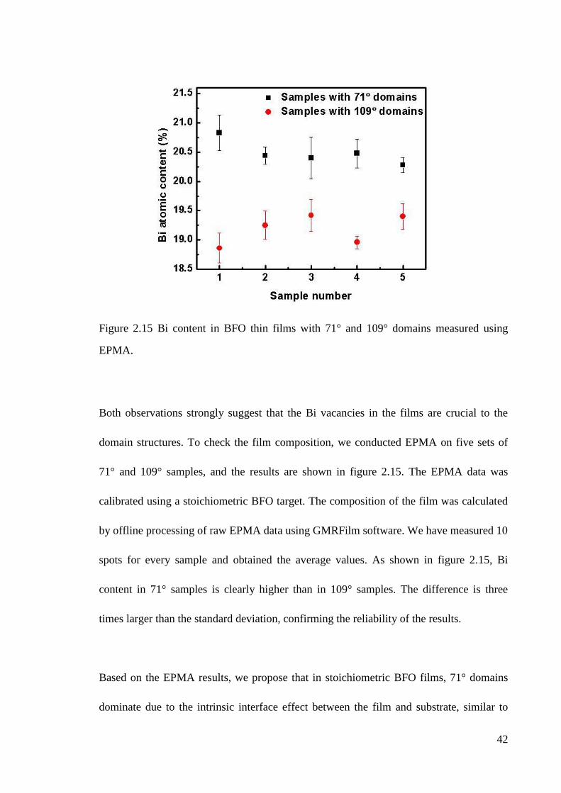
EPMA.
Both observations strongly suggest that the Bi vacancies in the films are crucial to the
domain structures. To check the film composition, we conducted EPMA on five sets of
71° and 109° samples, and the results are shown in figure 2.15. The EPMA data was
calibrated using a stoichiometric BFO target. The composition of the film was calculated
by offline processing of raw EPMA data using GMRFilm software. We have measured 10
spots for every sample and obtained the average values. As shown in figure 2.15, Bi
content in 71° samples is clearly higher than in 109° samples. The difference is three
times larger than the standard deviation, confirming the reliability of the results.
Based on the EPMA results, we propose that in stoichiometric BFO films, 71° domains
dominate due to the intrinsic interface effect between the film and substrate, similar to

43
that predicted for KNbO3 film on SrRuO3 coated substrate[89] or BFO film on LaSrMnO3
layer[91]. We know for the fully poled upward 71° domains, a large downward
depolarization field exists. This large downward depolarization field must be balanced by
an upward internal bias in the as-deposited films to make the domains stable. Here, we
assume the interface effects induce an upward internal bias which stabilizes the fully
poled 71° domains. When using BFO target with lower Bi content or depositing the film
at higher temperature, Bi vacancies will form in the thin films. We don’t have means to
analyze the distribution of Bi across the film thickness. However, based on the study by
Matthew F. Chisholm, et al., vacancies prefer to locate at the interface between the film
and substrate.[47] These negatively charged Bi vacancies at the interface could generate
an downward internal field that balances the interface effect, leading to 109° domains
formation under depolarization field.[93]
2.5 Conclusions
We have described our effort in controlling the domain structures in BFO thin films by
using BFO target with different Bi content or changing the deposition temperature. The
underlying mechanism is also discussed. we conclude that:
(i) High quality epitaxial BFO thin films with different domain structures can be
fabricated by tuning the target composition or the deposition temperature.
(ii) The results can be explained by a combined effect of the interface property and Bi
vacancies in the films. In stoichiometric BFO films, 71° domains dominate due to

44
the intrinsic interface effect between the film and substrate. When using BFO
target with lower Bi content or depositing the film at higher temperature, Bi
vacancies in the film induce another internal field that balances the interface
effect, leading to 109° domains formation under depolarization field.

45
Chapter 3 Photovoltaic property of BiFeO3 thin films with 109°
domains
Previous studies on ferroelectric photovoltaic effect mainly focused on BaTiO3 and
Pb(ZrTi)O3, whose band gaps correspond to the UV region. BFO, a multiferroic material
with robust ferroelectric and magnetic orders at room temperature[1] and a band gap
within visible light range[1], provides a unique opportunity for ferroelectric photovoltaic
effect study. Earlier work usually attribute the effect to the ferroelectric polarization
induced depolarization field, combined with other factors, such as band offsets at the
film/electrode interface[73], and defects in the thin film[94]. In 2010, Yang et al. reported
a very large photovoltage in BFO films with well aligned 71° domains.[3] The authors
proposed that the effect arises from the structurally driven electrostatic potential steps at
the nanometer-scale domain walls. Another study by Seidel et al. has reported that the
potential step at 109° domain walls is much larger than that at 71° domain walls.[61] It is
thus expected that BFO films with well aligned 109° domain walls will generate a
significantly larger photovoltage. However, macroscopic PV measurement of samples
with 109° domain walls is prohibited due to the presence of domains with IP polarizations
pointing in opposite directions (see figure 3.1 (b)), thus canceling the effect.
To investigate the photovoltaic property of BFO film with 109° domains, we tried to
control the domain patterns by using miscut orthorhombic DSO substrates. We have
successfully obtained BFO films with only two polarization variants forming 109°
domains, leading to a net IP polarization. The net polarization direction could be switched
46
by an external field using a quasi-planar setup.[95] Furthermore, by combining PFM
imaging with photovoltaic measurements, we have established a clear correlation between
the ferroelectric domain structures of BFO and its photovoltaic property.
3.1 Experimental procedure
BFO thin films with 109° domains are epitaxially grown on exact and miscut
orthorhombic DSO (110)o substrates. The lattice parameter a, b, and c of DSO are
5.44 Å, 5.71 Å, and 7.89 Å, respectively. The 2º miscut direction is along (001)o
direction. B0.8FeO3 target is used to grow films with 109º domains. The substrate and
target are prepared the same way as described previously.
The deposition oxygen pressure is 100 mtorr, and the substrate temperature is 750 ºC.
Following the BFO thin film deposition, electrode patterning is carried out following
standard photolithography technique. BFO film is cleaned using acetone and ethanol
subsequently before the photolithography followed by drying at 110 ºC for 2 minutes. We
first coat the film with a buffering layer of LOR 5A (Microchem®) using spin coater at
4000 rpm, followed by baking at 110 ºC for 2 minutes. After this, a top layer of positive
photoresist EPG 510 (Everlight®) is coated at 4000 rpm, followed by baking at 110 ºC for
2 minutes again. After the spin coating, the sample is attached to a photomask for UV
light (350 W) exposure for 6s using LithoPack 300 (SUSS MicroTec®). The sample is
developed in TMAH (Kanto®) solution for 18 seconds to remove the exposed photoresist.
40nm thick Pt electrodes are deposited by PLD. The deposition was conducted at room
temperature in vacuum (5×10⁻⁴ Pa), with a high laser density of 1 J/cm2 and a frequency

47
of 5 Hz. After the deposition of Pt, the remaining photoresist is removed by remover
solution (MicroChem®).
Polarization switching experiment is carried out using a commercial ferroelectric tester
(Radiant Technologies, Inc.). For the photovoltaic measurement, current-voltage (I-V)
curves are tested using a pA meter/DC voltage source (Hewlett Package 4140B). The
light source is a Halogen lamp and the illumination energy density was 20 mW/cm2. Each
time after the polarization switching, the I-V curve under light is measured, and then PFM
is conducted to observe the domain structure. Following this procedure, we try to
establish the correlation between photovoltaic effect and domain structure.
3.2 Photovoltaic property of BiFeO3 thin films with 109° domains
We use DSO (110)o single crystal as the substrates. The pseudo-cubic IP lattice constants
of DSO (a=3.951, b=3.946) are close to that of BFO. Similar to GSO substrates, the
asymmetric unit cell results in anisotropic stress in BFO films and a competition between
multiple structural variants for strain relaxation.[67, 87] The result is that two of the
structural variants are more favorable. However, even with two structural variants, the net
IP polarization can still point in opposite directions (see figure 3.1 (d) and (e)). Miscut
substrates are then used to generate a net IP polarization.

48
Figure 3.1 (a) Topography, (b) IP, (c) OOP PFM images of 109° BFO thin films on a
normal DSO substrate. (d) and (e) Schematic of polarization variants in the sample. (f)
Topography, (g) IP, and (h) OOP PFM images of 109° BFO thin films on a 2º miscut
DSO substrate. The arrow in (f) shows the miscut direction, and the arrow in (g) shows
the net IP polarization direction.
Figure 3.1 (a-c) shows the topography, IP and OOP PFM images of the BFO film grown
on a normal DSO substrate. Combining the IP and OOP domain images, we can
determine the local polarization direction as indicated in figure 3.1 (d) and (e). The bright
yellow stripe corresponds to P1+, the two brown stripes correspond to P2
- and P2+,
respectively, and the dark purple stripe corresponds to P1-. Looking at the IP PFM image

49
(figure 3.1 (b)), it is clear that there are 2 structural variants with 4 polarization variants
existing in this sample, and the IP polarization direction of the yellow-brown stripes is
opposite to that of the purple-brown stripes. Therefore the net IP polarization and the
potential steps across the 109° domain walls are cancelled, leading to negligible
photovoltage across the sample. On the other hand, if we use a DSO substrate with 2º
miscut towards (001)o direction (indicated by the arrow in figure 3.1 (f)), the polarization
variants are reduced to 2, as shown in figure 3.1 (g, h). The IP PFM image (figure 3.1 (g))
shows only two contrasts (yellow-brown stripes), with a very small content of
purple-brown stripes, while the OOP image (figure 3.1 (h)) shows bright-dark stripes.
This proves that 109° domains with P1+ and P2
- components dominate in this sample. This
can be understood by the effect of the step edges on the substrate surface introduced by
miscut.[86] When the first layer of BFO was deposited, the unit cells should start
nucleating along the step edges, where the vertical interface between BFO and DSO break
the IP symmetry, thus excluding 2 of 4 polarization variants. In this case, there is a net IP
polarization in the sample pointing to the miscut direction, as indicated in figure 3.1 (g).
Figure 3.2 Schematic of the planar Pt electrodes on BFO thin film and the demonstration
of electrical connection.

50
Planar electrodes are used for the measurement of photovoltaic property and the
polarization switching experiment, which allows observation of domain structure
evolution by PFM after polarization switching. Therefore, the correlation between the
domain structure and the photovoltaic property can be established. Figure 3.2 shows the
schematic of the planar device structure. Pt electrodes have a length of 500 µm, and a
width of 10 µm. The distance between two electrodes (channel width) is 5 µm. Pt
electrodes are parallel to the original domain stripes. When applying a voltage to the
device, the electric field is perpendicular to the original domain stripes and parallel to the
net IP polarization direction.[96]
Figure 3.3 Photovoltaic property of BFO sample with mainly two polarization variants of
109° domains. (a) I-V curves of the as-grown sample and the sample applied by different

51
voltages. (b) IP PFM image of as-prepared sample. (c)-(g) IP PFM images of the sample
applied by different voltages. The arrows show the net IP directions.
The I-V behavior of BFO films with net IP polarization is measured both in dark and
under white-light illumination (energy density, 20 mW/cm2). Under illumination, a photo
induced open-circuit voltage (Voc) of 0.5 V is obtained (figure 3.3 (a)), while no Voc was
observed in dark. To correlate the photovoltaic property with the domain structures of the
film, we conducted a switching experiment. By applying an external bias to the films
using the planar device, the sign of Voc can be switched. At the same time, we record the
IP domain images within the channel area (figure 3.3 (b-g)) (no change in OOP PFM
images is observed). When a negative voltage (electric field opposite to the original net IP
polarization direction) is applied to the electrodes, the original yellow-brown stripes turn
into purple-brown stripes. At -150 V, almost all the yellow-brown stripes have turned into
purple-brown ones (figure 3.3 (d)), indicating that the IP polarization is switched to the
opposite direction (see figure 3.3 (d, e, and f)). Accompanying the switching of
polarization, the Voc is changed to about -1.0 V. Further increase of the voltage leads to
complete switching of the polarization and the Voc saturates at about -1.1 V for this
device. By reversing the voltage polarity, the domain structure is switched back to its
original state, and the Voc returns to about 0.5 V. Note that the negative Voc is larger than
the corresponding positive value even after a much larger positive voltage (+350 V) is
applied. This could be due to the unswitched domains as shown in figure 3.3 (f, and g). It
is possible that these domains are pined by some defects in the film at the film-substrate
interface. Further study is needed to clarify the actual origin of domain pinning.

52
Figure 3.4 (a) Schematic of the polarization switching of 109° domains in BFO thin films.
(b) Schematic of the change of IP and OOP PFM images of the 109° stripe domains after
switching.
Figure 3.4 demonstrates that how polarization variants of 109º domain switch under an
external voltage. The PFM images reveal that P1+ switches to P2
+, while P2- switches to
P1- under the negative voltage. This proves that the IP polarization reversal is achieved by
71° rotation of the individual components, while the OOP polarization component does
not change during switching.

53
3.3 Mechanism of the photovoltaic response of BiFeO3 thin films with 109° domains
The domain density of our samples is about 40 /μm. For a 5 μm channel, there are about
200 domain walls. The largest open circuit voltage we have observed in our samples is
1.6 V, which leads to a potential drop of about 8 mV/domain. This value is comparable to
the microscopic measurement result reported by Yang et al.[3], but much smaller than the
theoretically predicted 150 mV/domain. Several reasons may contribute to the lower Voc
observed experimentally as listed below.
Figure 3.5 (a) Schematic of 109 domains, the circle demonstrates where the electrostatic
energy is high. (b) Schematic of vortex domains. Figure captured from [97].
First, the samples with mainly two polarization variants still contain small amount of
domains with opposite polarization direction. These domains will decrease the total net IP
polarization, and therefore inevitably reduces the photovoltage observed. Secondly, a
recent study reported that vortex domains form at the interface between BFO film with
109° domains and the substrate where the electrostatic energy is high.[97] As shown in
figure 3.5 (a), the electrostatic energy at the location (circled place) between the right two
109º domains and the substrate is high, and therefore vortex domains form to reduce the

54
electrostatic energy. As shown in the circle of figure 3.5 (b), the IP polarization of r1- and
r4+ is opposite to that of r1
+ and r4-. As a consequence, the total net IP polarization
decreases, which may reduce the open circuit photovoltage observed.[96]
The above two reasons cannot account for the large discrepancy between the
experimentally observed photovoltage and that predicted theoretically. It is likely that the
theoretical study has overestimated the effect of the domain walls, or it may not even be
related. For example, residual depolarization field could also explain our results. When
there is a net IP polarization, the unscreened polarization charge will generate a
depolarization field which points to the opposite direction. The residual depolarization
field in the film functions as the internal field which could separate electron-hole pairs
that are generated by light illumination, leading to the photovoltaic effect.[96]
3.4 Conclusions
We have obtained BFO films with 109º domains and investigated their photovoltaic
effect. The conclusions are:
(i) BFO domains with only 109º domains can be obtained by using miscut
orthorhombic DSO substrate. The switching experiments prove that the
polarization reversal of 109º domains is achieved by 71° rotation of the individual
components.

55
(ii) Photovoltage obtained in BFO thin film with 109º domain walls indicates a very
small electrostatic potential step (around 8 mV) at the domain wall, which is much
smaller than theoretical prediction. The results could also be explained by residual
depolarization field. Therefore, the theoretical study has possibly overestimated
the effect of the domain walls, or it may not even be related.

56
Chapter 4 Non-volatile memory based on ferroelectric photovoltaic
effect
The 2010 BCC Research report on semiconductor memory estimated that the global
market of memory was $46.2 billion in 2009, which will reach $79 billion in 2014.
Among them, the non-volatile memory market was about $12.8 billion, reaching $25.7
billion in 2014 at a compound annual growth rate of 15%.[98] The ever-increasing
demand has driven intensive research activities in this area. Currently, the non-volatile
memory market is dominated by magnetic hard disk drive (HDD) and Flash memory. The
HDD has a low read/write speed (>ms), which is why a dynamic random access memory
(DRAM) is needed to bridge the speed gap between HDD and CPU in our computers. At
present, Flash memory is widely used for portable electronics because of its low cost of
production and the well-developed semiconductor fabrication technology. However,
Flash memory has very low operation speed with ~10 µs programming and ~10 ms
erasing time.[99] Furthermore, it can only withstand ~105 rewriting cycles. These
drawbacks prevent it from becoming the primary storage device in personal computers.
A universal memory that combines the speed of DRAM and non-volatility of Flash
memory has long been the dream of electronic engineers. Several concepts are under
investigation, including resistive switching random access memory (ReRAM) based on
filamentary conduction and/or interface barrier modulation by defects,[100-102] phase
change memory[103-105] and magnetoresistive random access memory (MRAM)[106,
107] which uses tunneling magnetoresistance effect. Although they operate at higher

57
speed than Flash memory, all of them have the drawback of high energy consumption
which is detrimental for portable applications.
Ferroelectric random access memory (FeRAM) stores information using the spontaneous
polarization of ferroelectric materials. An external voltage pulse can switch the
polarization between two stable directions, representing “0” and “1”. It is non-volatile and
the read/write process is very fast, which can be completed within ns. However, despite
its great promise, FeRAM has a negligible share of today’s memory market. One problem
is that reading in conventional FeRAM is performed by applying a bias to the
ferroelectric capacitor and detecting the polarization switching current. This process is
destructive and a rewrite step is needed, leading to high energy consumption and reduced
device lifetime. Furthermore, it also requires a minimum capacitor size to generate
enough current for the sensing circuit, leading to low memory density. To realize the full
potential of FeRAM, alternative non-destructive read-out method is needed. Recently, the
resistance change of a ferroelectric tunnel junction upon polarization reversal has been
demonstrated and it can be used to sense the polarization direction
non-destructively.[108-110] However, this approach requires the ferroelectric layer to be
several nanometers thick at most, which poses a tremendous challenge on the device
fabrication. Furthermore, the stability of ferroelectricity in such a thin layer and fatigue
will cause reliability issues.
In this chapter, we demonstrate that the photovoltaic effect of a ferroelectric film can be
used to sense the polarization direction by simply reading the open circuit photovoltage or

58
short circuit photocurrent, and the device has superior performance even comparable to
that of DRAM. A prototype 16-cell memory based on the crossbar architecture has been
prepared and tested, demonstrating the scalability of this technique.[111]
4.1 Experimental Procedure
BFO films are epitaxially grown on miscut STO (001) substrates (4º miscut towards (110)
direction). (La0.7,Sr0.3)MnO3 (LSMO) and Fe are used as bottom and top electrode,
respectively, for the measurement of memory device. LSMO bottom electrode with the
thickness of 20 nm is deposited on miscut STO substrate by PLD at 670 °C with the
oxygen partial pressure of 300 mTorr. The laser energy density is fixed at 1 J/cm2, with a
frequency of 3 Hz. The growth parameters are optimized to make sure the surface
roughness is low. Following the deposition of the bottom electrode, epitaxial BFO film
was grown using a B0.8FO target with substrate temperature of 680 °C and oxygen partial
pressure of 50 mTorr. The laser energy density and reparation rate were 1J/cm2 and 10
Hz, respectively.
To prepare the top electrodes, an array of 5 µm ×5 µm squares are pattered on the BFO
film surface. After the photolithography, 5 nm-thick Fe electrode is deposited followed by
5 nm Pt to protect it from oxidation. Figure 4.1 shows the sketch of the square device
structure and the electrical connection. Transmittance of the Pt (5 nm)/Fe (5 nm)
electrode within visible spectrum is measured using UV-Vis spectroscopy as shown in
figure 4.2. About 35% of the light is transmitted, which means that the photovoltaic
signals can be further improved if transparent electrodes are used.

59
Figure 4.1 Experimental setup for the electrical characterizations of the individual
capacitors. LSMO and Pt/Fe are used as the bottom and top electrodes in both cases. A
four-probe micromanipulator is used to connect the device to a commercial ferroelectric
tester and PicoAmp meter/DC voltage source for P-V and I-V characterizations.
300 400 500 600 700 8000
10
20
30
40
50
Tra
ns
mit
an
ce
(%
)
Wavelength (nm)
d e m o d e m o d e m o d e m o d e m o
d e m o d e m o d e m o d e m o d e m o
d e m o d e m o d e m o d e m o d e m o
d e m o d e m o d e m o d e m o d e m o
d e m o d e m o d e m o d e m o d e m o
d e m o d e m o d e m o d e m o d e m o
d e m o d e m o d e m o d e m o d e m o
Figure 4.2 Transmittance of the Pt/Fe electrode at different wavelength measured by
using UV-Vis spectroscopy.

60
4.2 Basic properties of single domain BiFeO3
Figure 4.3 Basic properties of the STO substrate and single domain BFO films. (a)
Schematic of the miscut STO substrate and corresponding BFO growth, (b) 3-D
topography of the BFO film, (c) OOP PFM image of single-domain BFO film after
switching the central 2 × 2 µm2 area, the inset shows the polarization switching path, (d)
corresponding IP PFM image and cantilever orientation during scan.
To eliminate complications from multiple domains in BFO, we have used miscut
substrates (4° towards (110)) to obtain single domain films. Figure 4.3 (a) shows the
schematic of the miscut STO substrate and corresponding BFO growth, and figure 4.3 (b)
shows the 3-D topography of the BFO film. The film/substrate interface at the step edge
lifts the degeneracy of the multiple domains in BFO, and the preferred polarization
direction is indicated (see the yellow arrow in figure 4.3 (a)). Figure 4.3 (c) and (d) show
the OOP and IP PFM domain images of the BFO film, together with the cantilever
direction with respect to the film. The uniform contrasts (yellow color) of both OOP and
IP PFM images confirm that the as-grown films have single domain with polarization

61
direction as indicated in the BFO unit cell (yellow arrow). The preferred OP polarization
direction is well documented in the literature, likely a result of interface chemistry
between BFO and LSMO.[91] To clarify the polarization switching path of the film, a
positive DC bias of 9 V was applied to the cantilever tip during scanning over a 2 m by
2 m region. As a result, polarization switching occurs as shown in figure 4.3 (c) and (d).
Both the OOP and IP PFM images changed to purple color. Combining the OOP and IP
PFM images, it can be confirmed that the polarization switching is fulfilled by 180°
rotation (see inset of figure 4.3 (c), the purple arrow shows the domain after polarization
switching). Fe is chosen as the top electrode based on our investigation on the
polarization fatigue in BFO. We have learned that charge injection at the electrode/BFO
interface leads to domain pinning. When the pinned domains grow across the film,
macroscopic fatigue occurs.[112] Furthermore, our recent study has revealed that the
Schottky barrier at the interface is critical for the charge injection process. By using a low
work function metal to reduce the barrier height, charge injection can be greatly reduced
and fatigue performance significantly improved.[113]
Figure 4.4 (a) typical P-V loop of the Fe/BFO/LSMO capacitor (red line is the
corresponding I-V curve), and (b) I-V curves of the Fe/BFO/LSMO capacitor under dark
and light with opposite polarization directions.

62
-4 -2 0 2 4-100
-50
0
50
100
Po
lari
za
tio
n (C
/cm
2)
Voltage (V)
1 kHz
10 kHz
100 kHz
Figure 4.5 P-V loops measured at different frequencies.
The ferroelectric polarization-voltage (P-V) hysteresis loop shown in figure 4.4 (a)
reveals a remnant polarization of ~ 65 µC cm-2 along the [001] direction, which is
consistent with earlier reports.[1, 114] The red curve in figure 4.4 (a) is the relative I-V
curve, of which the two peaks show the switching current. The square shape of the loop
proves the good quality of the BFO film. The coercive voltage is quite small, about 1.3 V,
which can be further reduced by decreasing the film thickness. Lower coercive voltage
can reduce the energy consumption that is needed to write the memory device to ON or
OFF states. The measurement frequency of the P-V loop is 1 kHz. The frequency
dependence of the P-V loop is shown in figure 4.5. The ferroelectric property of the BFO
films has been measured under various frequencies from 1 kHz to 100 kHz. The coercive
field increases as measurement frequency increases, consistent with previous
reports.[111]

63
For our device, the applied voltage is termed positive (negative) if a positive (negative)
bias is applied to the top electrode. After poling the polarization up (down) by applying a
voltage pulse of -3 V (+3 V), the I-V curves demonstrate clear photovoltaic effect under
light (light source: Halogen lamp; energy density: 20 mW/cm2). As shown in figure 4.4
(b), when polarization points upward, the Isc was ~ -0.15 pA and the Voc was ~ +0.22 V.
After the polarization was switched, the photovoltaic effect was reversed with Isc of ~
+0.16 pA and Voc of ~ -0.12 V. It is thus possible to determine the polarization direction
(stored information) by sensing the photovoltage or photocurrent, and this process is
non-destructive. The switchable nature of the photovoltaic effect implies that it is related
to the spontaneous polarization of BFO. This has been discussed in details in the
literature.[16, 70, 72, 94] Basically, due to incomplete compensation of the polarization
charges, the residual depolarization field is always in the opposite direction of the
polarization. The depolarization field drives the photo-generated electron-hole pairs into
opposite direction before they recombine. The asymmetric Voc and Isc under positive and
negative polarization directions is likely due to the different work functions of the top and
bottom electrodes, which also induces an internal field that does not depend on the
polarization direction.

64
4.3 Properties of the Fe/BiFeO3/(La0.7,Sr0.3)MnO3 memory cells
Figure 4.6 Photovoltaic property of the Fe/BFO/LSMO device. Current-voltage curves
measured under different light intensity for (a) polarization down and (b) up states. (c)
Open circuit voltage and (d) short circuit current as functions of light intensity for both
polarization directions.
The influence of the light intensity on the photovoltaic property was tested with the light
intensity increasing from 5 to 20 mW/cm2. As expected, the photovoltaic response of the
device depends on the intensity of the light. When the light intensity increases, both Voc
and Isc increase (figure 4.6 (a-d)). The Voc of the device with upward polarization saturates
at ~ +0.21 V, and the Voc of the device with downward polarization saturates at ~ -0.12 V.
No saturation was observed for Isc up to 20 mV/cm2. The fact that the Voc and Isc increase
with the increase of light intensity is consistent with previous report.[3] Increasing light

65
intensity can generate more electron-hole pairs which are separated by the internal field
and lead to larger Voc and Isc.[3] For the measurement of Voc, the circuit is open. The
electrons and holes that are separated by the internal field will accumulate at the two
electrodes, which will generate an electric field opposite to the internal field. When the
built-in internal field is totally cancelled, photo-generated electron-hole pairs cannot be
separated any longer, therefore Voc saturates at this point. However, Isc will not saturate
with the increase of the light intensity. When measuring Isc, the loop is short circuited.
The separated electrons and holes will flow in the circuit,. As the light intensity increases,
the fixed internal field can keep separating increasing electron-hole pairs, which thus
leads to larger Isc.
Figure 4.7 Influence of poling pulse width on (a) Voc, and (b) Isc of the capacitors. The
switching voltage changes from ± 3 V to ± 6 V.
Operation speed is an important factor that defines the performance of memory device.
To assess the operation speed of the memory cells, we measured the influence of the

66
poling pulse width on the photovoltaic response and the results are shown in figure 4.7.
Square pulses of 1 ns to 1 ms (generated by pulse generator (Keithley 3401) are used to
control the polarization direction of the film, and the I-V curves under 20 mW/cm2 light
are measured subsequently. When 6 V pulses are applied, the spontaneous polarization
starts to switch within several ns. At 10 ns, the polarization is fully reversed and both Voc
and Isc reach expected values. This result demonstrates that the memory cell can be
written within 10 ns. However, this is by no means the limit. In fact, polarization
switching by pulses of <1 ns has been reported in the literature, with the ultimate limit
being set by the acoustic phonon mode (velocity of sound) in the material.[115] For the
reading process, since it does not require switching of polarization and the light can be
kept on whenever the device is in operation, so the photovoltaic response of every cell is
always ready for reading and the speed is only limited by the RC-time constant of the
circuit. What’s even more attractive is that, if we use Voc as the sensing signal, the
memory cell can be as small as lithography technique allows since Voc does not depend on
the lateral size of the capacitor.

67
Figure 4.8 Retention and fatigue behavior of the Fe/BFO/LSMO memory cell. (a) Open
circuit voltage and (b) short circuit current for both polarization directions show
negligible change after 4 months. (c) Polarization-voltage loops and (d) Current-voltage
curves measured after repetitive switching by pulses of ±3 V, 1 ms reveal no fatigue after
108 cycles. (e) Open-circuit voltage and (f) Short-circuit show slight change after the
switching cycles of 108. In (a,b,d,e,f), blue: under light with polarization up; red: under
light with polarization down.
For non-volatile memory application, long data retention and good fatigue resistance are
two critical requirements. We have monitored the Voc and Isc of several memory cells for
4 months, no deterioration in the signal has been observed (figure 4.8 (a and b)).
Furthermore, the memory cells have been subjected to bipolar switching for up to 108
cycles and show no sign of fatigue (figure 4.8 (c-f)). It is also well known in the
ferroelectric community that fatigue can be mitigated by using oxide electrodes,
68
suggesting that the non-volatile memory can sustain much more read/write cycles than
Flash memory.
4.4 Properties of a prototype memory device
To access the scalability of the photovoltaic effect based FeRAM, we have prepared and
tested a prototype memory using the cross-bar architecture. The bottom LSMO film was
patterned through photolithography process and chemical etching. After developing,
LSMO electrodes with the pattern of 2000 µm × 10 µm stripes were protected by the
photoresist layer. The rest of LSMO film was etched in a IBr/HCl solution of which the
volume ratio of HCl to IBr is 9. Then the remaining photoresist was removed by remover.
After this, the STO substrate with LSMO electrodes was cleaned by acetone and ethanol.
At last, BFO film was deposited on the top of LSMO electrodes using the same
deposition parameters mentioned in chapter 4.1. After the deposition of BFO film, its
surface was pattered with Fe electrodes. The top stripe Fe electrodes are of the same size
as the bottom LSMO electrodes but in the perpendicular direction. So a capacitor with a
size of 10 × 10 µm is formed. The preparation procedure of the top Fe electrodes is same
as that of the square Fe electrodes above in this chapter. After the deposition of top
electrode, the remaining photoresist was removed by remover solution (MicroChem®).
The schematic of the 4 × 4 cross bar device and the demonstration of the electrical
connection are shown in figure 4.9.

69
Figure 4.9 Schematic of the cross bar device structure and the demonstration of the
electrical connection.
Figure 4.10 Performance of a prototype 16 cell memory based on the cross bar
architecture. (a) Topography of the device with preset polarization direction indicated.
Blue: polarization up, Red: polarization down. (b) Open circuit voltages of all 16 cells
indicated. These are measured under 20 mW/cm2 light. Blue: positive photovoltage, Red:
negative photovoltage.
Figure 4.10 (a) depicts the topographic image of the device and each junction represents a
memory cell. The 4 × 4 cross bar structure creates 16 cells in the device. In figure 4.10
(a), junctions with blue color represent memory cells with the polarization of BFO film

70
pointing up, while junctions with red color represent memory cells with the polarization
pointing down. Despite the large size of each cell, limited by our lithography facility, all
of them are fully functional. After poling the polarization direction in each cell randomly,
we read the Voc under 20 mW/cm2 light by measuring the I-V curve of each cell. The
results are shown in figure 4.10 (b). Memory cells with upward polarization show positive
Voc while cells with downward polarization show negative Voc. The absolute values are
slightly different from those obtained from the single capacitors. But the results clearly
demonstrate the scalability of this concept. Typical memory performance, i.e., data
retention and fatigue, has been tested for the cross bar device. The results are similar to
that of the single capacitors figure 4.11.
Figure 4.11 Retention and fatigue behavior of the 4 × 4 cross bar memory cell. (a) Open
circuit voltage and (b) short circuit current for both polarization directions show
negligible change after 2 months. (c) Polarization-Electric field loops and (d)
Current-voltage curves measured after repetitive switching by pulses of ±3 V, 1 ms reveal

71
no fatigue after 107 cycles. (e) Open-circuit voltage and (f) Short-circuit current show
little change after 107 cycles. It is also well known in the ferroelectric community that
fatigue can be mitigated by using oxide electrodes, suggesting that the non-volatile
memory can sustain much more read/write cycles than Flash memory. In (a,b,d,e,f), blue:
under light with polarization up; red: under light with polarization down.
A fundamental problem for the cross-bar architecture is that sneak paths may form which
bypass the target memory cell being addressed. Practically, this can be prevented by
integrating a transistor with each cell even though it reduces the memory density. In fact,
the 1 transistor 1 capacitor (1T1C) structure is employed in conventional ferroelectric
memory. However, in the proposed device, each cell generates Voc and Isc under light by
itself. No external driving force is needed during the reading process. The sneak path
problem is rather different from that in the Memresistive cross bar memory. Further study
is underway to clarify this issue. We also hope that this study may inspire other groups to
tackle this problem as well.

72
Table 4.1 Comparison between different memory technologies.[108]
# Estimated from the DRAM cell size, since the transistor size dominates if using Voc as
the read out signal.
* Based on current study.
^ Based on existing result on polarization retention and fatigue in the literature.
$ Since the light is on continuously during the memory operation, there is a standby
power consumption. For a 1G memory with 50nm feature size and 11F2 fill factor, the
standby power consumption is about 5.5 mW.
The non-volatile memory proposed in this paper offers several advantages over other
technologies (Table 4.1). For example, the feature size is only limited by the lithography
technology if photovoltage is used as the sensing signal. Compared with Flash memory,
the photovoltaic FeRAM reported here has much higher operation speed and lower
energy consumption. The memory density is higher than MRAM and conventional
FeRAM. Writing time of less than 10 ns has been demonstrated, much faster than MRAM
and Flash. The power consumption is much less than MRAM and phase change memory
(PCM). Note that the results reported here are obtained from typical BFO capacitors as

73
proof of concept. Further optimization on the film thickness and electrode materials
selection could improve the Voc and Isc for better performance. For example, using
electrodes with larger screening length should enhance Voc due to increasing
depolarization field. Furthermore, the concept is not limited to BFO. Other ferroelectric
materials, e.g., Pb(ZrTi)O3 and BaTiO3, should give rise to similar behavior. In summary,
we report here a novel approach to create a non-volatile memory technology that uses the
polarization dependent photovoltaic effect in ferroelectrics.[111]
4.5 Conclusions
We have investigated the properties of Fe/BFO/LSMO capacitors as possible non-volatile
memory, where the stored information can be read non-destructively by sensing the
photovoltaic responses. The conclusions are:
(i) Photocurrent and photovoltage with opposite signs can be obtained by
controlling the polarization direction of the Fe/BFO/LSMO capacitors.
Coupling the photovoltaic effect with the ferroelectric polarization allows
non-destructive readout of the stored information.
(ii) The memory cells can be written within 10 ns. The reading speed is only
limited by the circuit, and the read voltage is 0. Moreover, the Fe/BFO/LSMO
memory cells have good data retention and fatigue resistance properties. No
deterioration has been observed after four months. The memory cells have

74
been subjected to voltage cycling for up to 108 cycles and show no sign of
fatigue.
(iii) The results reported here are obtained from typical BFO capacitors as proof of
concept. Further optimization on the film thickness and electrode materials
selection could improve the Voc and Isc obtained for better performance.

75
Chapter 5 Summary and Future Work
5.1 Summary
In this project, we have achieved precise control of the domain structures in BFO thin
films by tuning the target composition and deposition temperature. The photovoltaic
property of BFO thin films with regular 109° domains is studied. We conclude that the
theoretical study has overestimated the energy band bending at the domain walls. Finally,
we explored the possibility of using ferroelectric photovoltaic effect in non-volatile
memory. The conclusions are:
(i) BFO thin films with 71° or 109° domains can be obtained by using BFO targets
with different Bi content or changing the deposition temperature. Decreasing Bi
content in the target or increasing the deposition temperature changes the domain
structure of BFO from 71° to 109°. The results can be explained by a combined
effect of the interface property and Bi vacancies in the films.
(ii) BFO thin films that contain regular 109° domains with mainly two polarization
variants can be fabricated by using miscut DSO substrates. Photovoltaic effect of
such films has been investigated. A direct correlation between the 109° domains
switching and the photovoltaic response of the films is established, by conducting
PFM study using a planar device. The photovoltage is switchable upon
polarization reversal, and the IP polarization reversal of 109° domains is proven to
be achieved by 71° rotation of each component. The obtained photovoltage

76
indicates a very small electrostatic potential step at the domain wall. It is likely
that the theoretical study has overestimated the effect of the domain walls, or it
may not even be related, since residual depolarization field could also explain the
results.
(iii) Fe/BFO/LSMO capacitors are prepared as photovoltaic FeRAM cells since the
photovoltaic responses depend on the polarization direction. It enables
non-destructive read-out of the stored information (polarization direction). The
memories have very high operation speed (within 10 ns), low energy consumption
, and zero read voltage. Moreover, they demonstrate good data retention and
fatigue resistance properties. No deterioration in the signal of Voc and Isc has been
observed within four months, and the cells have been subjected to voltage cycling
for up to 108 cycles and show no sign of fatigue. A prototype 4×4 cross bar
devices have been prepared and tested, demonstrating the scalability of this novel
technique.
5.2 Future Work
5.2.1 Enhancing the photovoltaic efficiency
Ferroelectric photovoltaic effect has potential applications in various fields. However, the
efficiency is low, mainly limited by the large band gaps of ferroelectric and the small
photocurrent densities.

77
The band gap of BFO is 2.7 eV, and its corresponding wavelength is within the visible
light range (460 nm). Although it is quite small among ferroelectrics, it can still be
reduced by doping. A reduced band gap could enhance the visible light absorption, and
thus increase the photovoltaic efficiency. Under light illumination, the photo generates a
fixed amount of electron-hole pairs. How many charges could be separated and move to
the electrodes depends on how large the internal electric field is. Therefore, increasing the
depolarization field could increase the Voc. To achieve this, we suggest using electrodes
with larger screening length. In this case, the more unscreened bound charges will
generate larger depolarization field, and thus larger Voc.
5.2.2 Further development of the photovoltaic FeRAM device
Despite the superior performance of photovoltaic FeRAM demonstrated in this study,
there are still challenges to overcome before it can be used. One of them is the large
resistance of the BFO film, which prevents a direct sensing of the photovoltage. We will
explore Ca doping to reduce the internal resistance of the film while maintaining its large
polarization. Another issue is the fatigue property of the device. It is well known that
oxide electrodes could improve the fatigue peformance of ferroelectrics. It has been
suggested that oxide electrodes can decrease the oxygen vacancy concentration at the
film/electrode interface and thus reduce the domain pinning. Therefore, we will try
different oxide electrodes to improve the fatigue property of the memory cells.

78
5.2.3 Sneak path problem in the cross bar device.
Further study will also be done on the sneak path issue which is inherent to the cross bar
architecture. Different from the memresistive cross bar memory, in our proposed device,
each cell at the junction generates the photovoltage or photocurrent by itself. No external
deriving source is needed during the reading process. Therefore, memory cells with
simple 1 × 4 and 2 × 2 crossbar structure will be fabricated to investigate whether or how
each cell affects each other. For example, the property of one cell will be studied while
poling three other cells to different polarizations. We can also conduct simulations to
investigate the effect of parallel paths on the read-out signals.

79
Reference
1. Wang, J., et al., Epitaxial BiFeO3 multiferroic thin film heterostructures. Science,
2003. 299(5613): p. 1719-1722.
2. Ihlefeld, J.F., et al., Optical band gap of BiFeO3 grown by molecular-beam
epitaxy. Applied Physics Letters, 2008. 92(14): p. 3.
3. Yang, S.Y., et al., Above-bandgap voltages from ferroelectric photovoltaic devices.
Nature Nanotechnology, 2010. 5(2): p. 143-147.
4. Seidel, J., et al., Domain Wall Conductivity in La-Doped BiFeO3. Physical Review
Letters, 2010. 105(19): p. 197603.
5. Fridkin, V.M., Bulk photovoltaic effect in noncentrosymmetric crystals.
Crystallography Reports, 2001. 46(4): p. 654-658.
6. Peumans, P., S. Uchida, and S.R. Forrest, Efficient bulk heterojunction
photovoltaic cells using small-molecular-weight organic thin films. Nature, 2003.
425(6954): p. 158-162.
7. Chynoweth, A.G., Surface Space-Charge Layers in Barium Titanate. Physical
Review, 1956. 102(3): p. 705-714.
8. Kholkin, A., O. Boiarkine, and N. Setter, Transient photocurrents in lead
zirconate titanate thin films. Applied Physics Letters, 1998. 72(1): p. 130-132.
9. Qin, M., et al., Stability of photovoltage and trap of light-induced charges in
ferroelectric WO3-doped (Pb0.97La0.03)(Zr0.52Ti0.48)O3 thin films. Applied Physics
Letters, 2007. 91(9): p. 092904.
10. Zheng, F., et al., Separation of the Schottky barrier and polarization effects on the
photocurrent of Pt sandwiched Pb(Zr0.20Ti0.80)O3 films. Applied Physics Letters,
2008. 93(17): p. 172101.
11. Yao, K., et al., Large photo-induced voltage in a ferroelectric thin film with
in-plane polarization. Applied Physics Letters, 2005. 87(21): p. 212906.
12. Qin, M., K. Yao, and Y.C. Liang, Photovoltaic mechanisms in ferroelectric thin
films with the effects of the electrodes and interfaces. Applied Physics Letters,
2009. 95(2): p. 022912.
13. Qin, M., et al., Thickness effects on photoinduced current in ferroelectric
(Pb0.97La0.03)(Zr0.52Ti0.48)O3 thin films. Journal of Applied Physics, 2007. 101(1): p.
014104-014108.
14. Pintilie, L., et al., Short-circuit photocurrent in epitaxial lead zirconate-titanate
thin films. Journal of Applied Physics, 2007. 101(6): p. 064109-064109-8.
15. Yang, Y.S., et al., Schottky barrier effects in the photocurrent of sol--gel derived
lead zirconate titanate thin film capacitors. Applied Physics Letters, 2000. 76(6):
p. 774-776.
16. Lee, D., et al., Polarity control of carrier injection at ferroelectric/metal
interfaces for electrically switchable diode and photovoltaic effects. Physical
Review B, 2011. 84(12): p. 125305.
17. Pintilie, L., et al., Bi4Ti3O12 ferroelectric thin film ultraviolet detectors. Applied
Physics Letters, 1998. 73(3): p. 342.
18. Shan, X.C., et al., Fabrication of X-ray masks and applications for optical switch
molding. Sensors and Actuators A: Physical, 2003. 108(1–3): p. 224-229.

80
19. Maeda, R., et al., Piezoelectric Microactuator Devices. Journal of Electroceramics,
2004. 12(1-2): p. 89-100.
20. Scott, J.F. and C.A. Paz de Araujo, Ferroelectric Memories. Science, 1989.
246(4936): p. 1400-1405.
21. Ichiki, M., et al., Photovoltaic effect of lead lanthanum zirconate titanate in a
layered film structure design. Applied Physics Letters, 2004. 84(3): p. 395-397.
22. Teague, J.R., R. Gerson, and W.J. James, Dielectric hysteresis in single crystal
BiFeO3. Solid State Communications, 1970. 8(13): p. 1073-1074.
23. Rivera, J.P. and H. Schmid, On the birefringence of magnetoelectric BiFeO3.
Ferroelectrics, 1997. 204(1): p. 23-33.
24. Kubel, F. and H. Schmid, Structure of a ferroelectric and ferroelastic
monodomain crystal of the perovskite BiFeO3. Acta Crystallographica Section B,
1990. 46(6): p. 698-702.
25. Neaton, J.B., et al., First-principles study of spontaneous polarization in
multiferroic BiFeO3. Physical Review B, 2005. 71(1): p. 014113.
26. Zavaliche, F., et al., Ferroelectric domain structure in epitaxial BiFeO3 films.
Applied Physics Letters, 2005. 87(18): p. 182912.
27. Li, Y.L., S.Y. Hu, and L.Q. Chen, Ferroelectric domain morphologies of (001)
PbZr1 - xTixO3 epitaxial thin films. Journal of Applied Physics, 2005. 97(3): p.
034112-034117.
28. Zavaliche, F., et al., Multiferroic BiFeO3 films: domain structure and polarization
dynamics. Phase Transitions, 2006. 79(12): p. 991-1017.
29. Ederer, C. and N.A. Spaldin, Effect of Epitaxial Strain on the Spontaneous
Polarization of Thin Film Ferroelectrics. Physical Review Letters, 2005. 95(25): p.
257601.
30. Lebeugle, D., et al., Very large spontaneous electric polarization in BiFeO3 single
crystals at room temperature and its evolution under cycling fields. Applied
Physics Letters, 2007. 91(2): p. 022907.
31. Lebeugle, D., et al., Room-temperature coexistence of large electric polarization
and magnetic order in BiFeO3 single crystals. Physical Review B, 2007. 76(2): p.
024116-024120.
32. Kim, D.H., et al., Effect of epitaxial strain on ferroelectric polarization in
multiferroic BiFeO3 films. Applied Physics Letters, 2008. 92(1): p. 012911.
33. Jang, H.W., et al., Strain-Induced Polarization Rotation in Epitaxial (001) BiFeO3
Thin Films. Physical Review Letters, 2008. 101(10): p. 107602.
34. Chu, Y.H., et al., Controlling magnetism with multiferroics. Materials Today,
2007. 10(10): p. 16-23.
35. Sosnowska, I., T. Peterlinneumaier, and E. Steichele, Spiral magnetic-ordering in
bismuth ferrite. Journal of Physics C-Solid State Physics, 1982. 15(23): p.
4835-4846.
36. Lebeugle, D., et al., Electric-field-induced spin flop in BiFeO3 single crystals at
room temperature. Physical Review Letters, 2008. 100(22): p. 227602.
37. Catalan, G. and J.F. Scott, Physics and applications of bismuth ferrite. Advanced
Materials, 2009. 21(24): p. 2463-2485.
38. Eerenstein, W., et al., Comment on "Epitaxial BiFeO3 multiferroic thin film
heterostructures". Science, 2005. 307(5713): p. 1203-1203.

81
39. Béa, H., et al., Investigation on the origin of the magnetic moment of BiFeO3 thin
films by advanced x-ray characterizations. Physical Review B, 2006. 74(2): p.
020101.
40. Ederer, C. and N.A. Spaldin, Weak ferromagnetism and magnetoelectric coupling
in bismuth ferrite. Physical Review B, 2005. 71(6): p. 060401.
41. Zhao, T., et al., Electrical control of antiferromagnetic domains in multiferroic
BiFeO3 films at room temperature. Nature Materials, 2006. 5(10): p. 823-829.
42. Chu, Y.H., et al., Electric-field control of local ferromagnetism using a
magnetoelectric multiferroic Nature Materials, 2008. 7(8): p. 678-678.
43. Bibes, M. and A. Barthelemy, Multiferroics: Towards a magnetoelectric memory.
Nature Materials, 2008. 7(6): p. 425-426.
44. Ho Won, J., et al., Domain Engineering for Enhanced Ferroelectric Properties of
Epitaxial (001) BiFeO3 Thin Films. Advanced Materials, 2009. 21(7): p. 817-823.
45. Streiffer, S.K., et al., Domain patterns in epitaxial rhombohedral ferroelectric
films. I. Geometry and experiments. Journal of Applied Physics, 1998. 83(5): p.
2742-2753.
46. Wang, R.V., et al., Reversible chemical switching of a ferroelectric film. Physical
Review Letters, 2009. 102(4): p. 047601.
47. Chisholm, M.F., et al., Atomic-scale compensation phenomena at polar interfaces.
Physical Review Letters, 2010. 105(19): p. 197602.
48. Goltsev, A.V., et al., Structure and Interaction of Antiferromagnetic Domain
Walls in Hexagonal YMnO3. Physical Review Letters, 2003. 90(17): p. 177204.
49. Přívratská, J. and V. Janovec, Spontaneous polarization and/or magnetization in
non-ferroelastic domain walls: symmetry predictions. Ferroelectrics, 1999. 222(1):
p. 23-32.
50. Přívratská, J. and V. Janovec, Pyromagnetic domain walls connecting
antiferromagnetic non-ferroelastic magnetoelectric domains. Ferroelectrics, 1997.
204(1): p. 321-331.
51. Floquet, N. and C. Valot, Ferroelectric domain walls in BaTiO3: Structural wall
model interpreting fingerprints in XRPD diagrams. Ferroelectrics, 1999. 234(1): p.
107-122.
52. Padilla, J., W. Zhong, and D. Vanderbilt, First-principles investigation of 180°
domain walls in BaTiO3. Physical Review B, 1996. 53(10): p. R5969-R5973.
53. Meyer, B. and D. Vanderbilt, Ab initio study of ferroelectric domain walls in
PbTiO3. Physical Review B, 2002. 65(10): p. 104111.
54. Houchmandzadeh, B., J. Lajzerowicz, and E. Salje, Order parameter coupling and
chirality of domain walls. Journal of Physics-Condensed Matter, 1991. 3(27): p.
5163-5169.
55. Tokunaga, Y., et al., Composite domain walls in a multiferroic perovskite ferrite.
Nature Materials, 2009. 8(7): p. 558-562.
56. Rubi, D., et al., Ferromagnetism and increased ionicity in epitaxially grown
TbMnO3 films. Physical Review B, 2009. 79(10): p. 014416.
57. Venkatesan, S., et al., Nanoscale domain evolution in thin films of multiferroic
TbMnO3. Physical Review B, 2009. 80(21).

82
58. Logginov, A.S., et al., Room temperature magnetoelectric control of
micromagnetic structure in iron garnet films. Applied Physics Letters, 2008.
93(18): p. 182510.
59. Lykah, V.A., Domains and domain walls in multiferroic ferroelectric-ferromagnet
and control of its modulation. Ferroelectrics, 2010. 398(1): p. 71-76.
60. Kagawa, F., et al., Dynamics of multiferroic domain wall in spin-cycloidal
ferroelectric DyMnO3. Physical Review Letters, 2009. 102(5): p. 057604.
61. Seidel, J., et al., Conduction at domain walls in oxide multiferroics. Nature
Materials, 2009. 8(3): p. 229-234.
62. Lubk, A., S. Gemming, and N.A. Spaldin, First-principles study of ferroelectric
domain walls in multiferroic bismuth ferrite. Physical Review B, 2009. 80(10): p.
104110.
63. Daraktchiev, M., G. Catalan, and J.F. Scott, Landau Theory of Ferroelectric
Domain Walls in Magnetoelectrics. Ferroelectrics, 2008. 375(1): p. 122-131.
64. Zhang, J.X., et al., Computer simulation of ferroelectric domain structures in
epitaxial BiFeO3 thin films. Journal of Applied Physics, 2008. 103(9): p. 094111.
65. Chu, Y.H., et al., Ferroelectric size effects in multiferroic BiFeO3 thin films.
Applied Physics Letters, 2007. 90(25): p. 3.
66. Daumont, C.J.M., et al., Tuning the atomic and domain structure of epitaxial films
of multiferroic BiFeO3. Physical Review B, 2010. 81(14): p. 144115.
67. Chu, Y.H., et al., Nanoscale domain control in multiferroic BiFeO3 thin films.
Advanced Materials, 2006. 18(17): p. 2307.
68. Chu, Y.-H., et al., Nanoscale Control of Domain Architectures in BiFeO3 Thin
Films. Nano Letters, 2009. 9(4): p. 1726-1730.
69. Ihlefeld, J.F., et al., Optical band gap of BiFeO3 grown by molecular-beam
epitaxy. Applied Physics Letters, 2008. 92(14): p. 142908.
70. Choi, T., et al., Switchable Ferroelectric Diode and Photovoltaic Effect in BiFeO3.
Science, 2009. 324(5923): p. 63-66.
71. Wei, J., Y. Kui, and C.L. Yung, Bulk Photovoltaic Effect at Visible Wavelength in
Epitaxial Ferroelectric BiFeO3 Thin Films. Advanced Materials, 2009. 22(15): p.
1763-1766.
72. Yi, H.T., et al., Mechanism of the switchable photovoltaic effect in ferroelectric
BiFeO3. Advanced Materials, 2011. 23(30): p. 3403-3407.
73. Yang, S.Y., et al., Photovoltaic effects in BiFeO3. Applied Physics Letters, 2009.
95(6): p. 062909.
74. Seidel, J., et al., Efficient Photovoltaic Current Generation at Ferroelectric
Domain Walls. Physical Review Letters, 2011. 107(12): p. 126805.
75. Brody, P. and F. Crowne, Mechanism for the high voltage photovoltaic effect in
ceramic ferroelectrics. Journal of Electronic Materials, 1975. 4(5): p. 955-971.
76. Glass, A.M., D.v.d. Linde, and T.J. Negran, High-voltage bulk photovoltaic effect
and the photorefractive process in LiNbO3. Applied Physics Letters, 1974. 25(4):
p. 233-235.
77. Brody, P., Ferroelectric photovoltaic method and apparatus for transferring
information, U.S. Patent, Editor. 1978. p. 4103341.
78. Chiu, Y.-P., et al., Atomic-Scale Evolution of Local Electronic Structure Across
Multiferroic Domain Walls. Advanced Materials, 2011: p. 1530-1534.

83
79. Lowndes, D.H., et al., Synthesis of novel thin-film materials by pulsed laser
deposition. Science, 1996. 273(5277): p. 898-903.
80. Christen, H.M. and G. Eres, Recent advances in pulsed-laser deposition of
complex oxides. Journal of Physics-Condensed Matter, 2008. 20(26): p. 264005.
81. Ashfold, M.N.R., et al., Pulsed laser ablation and deposition of thin films.
Chemical Society Reviews, 2004. 33(1): p. 23-31.
82. Martin, L.W., Y.H. Chu, and R. Ramesh, Advances in the growth and
characterization of magnetic, ferroelectric, and multiferroic oxide thin films.
Materials Science and Engineering: R: Reports, 2010. 68(4-6): p. 89-133.
83. You, L., Electrical control of ferromagnetism in multiferroic bismuth
ferrite-based heterostructures, in School of Materials Science and Engineering.
2011, Nanyang Technological University. p. 38.
84. Bea, H., et al., Influence of parasitic phases on the properties of BiFeO3 epitaxial
thin films. Applied Physics Letters, 2005. 87(7): p. 072508.
85. You, L., et al., Influence of oxygen pressure on the ferroelectric properties of
epitaxial BiFeO3 thin films by pulsed laser deposition. Physical Review B
(Condensed Matter and Materials Physics), 2009. 80(2): p. 024105.
86. Sichel, R.J., et al., Anisotropic relaxation and crystallographic tilt in BiFeO3 on
miscut SrTiO3 (001). Applied Physics Letters, 2010. 96(5): p. 051901.
87. Chu, Y.H., et al., Domain control in mulfiferroic BiFeO3 through substrate
vicinality. Advanced Materials, 2007. 19(18): p. 2662.
88. Folkman, C.M., et al., Stripe domain structure in epitaxial (001) BiFeO3 thin films
on orthorhombic TbScO3 substrate. Applied Physics Letters, 2009. 94(25): p.
251911.
89. Duan, C.G., et al., Interface effect on ferroelectricity at the nanoscale. Nano
Letters, 2006. 6(3): p. 483-487.
90. Singh-Bhalla, G., et al., Built-in and induced polarization across LaAlO3/SrTiO3
heterojunctions. Nature Physics, 2011. 7(1): p. 80-86.
91. Yu, P., et al., Interface control of bulk ferroelectric polarization. Proceedings of
the National Academy of Sciences of the United States of America, 2012.109(25):
p.9710.
92. Yuan, G.L., et al., The dependence of oxygen vacancy distributions in BiFeO3
films on oxygen pressure and substrate. Applied Physics Letters, 2009. 95(1): p.
012904.
93. Guo, R., et al., Influence of target composition and deposition temperature on the
domain structure of BiFeO3 thin films. AIP Advances. 2(4): p. 042104-7.
94. Ji, W., K. Yao, and Y.C. Liang, Bulk photovoltaic effect at visible wavelength in
epitaxial ferroelectric BiFeO3 thin films. Advanced Materials, 2010. 22(15): p.
1763-1766.
95. You, L., et al., Polarization switching in quasiplanar BiFeO3 capacitors. Applied
Physics Letters, 2010. 97(6): p.062910-1.
96. Guo, R., et al., Photovoltaic property of BiFeO3 thin films with 109 degrees
domains. Applied Physics Letters, 2011. 99(12): p.122902-1.
97. Nelson, C.T., et al., Spontaneous Vortex Nanodomain Arrays at Ferroelectric
Heterointerfaces. Nano Letters, 2011. 11(2): p. 828-834.
98. Semiconductor memory: technologies and global markets. 2010.

84
99. Sun Il, S., et al., SONOS-type flash memory cell with metal/Al2O3/SiN/Si3N4/Si
structure for low-voltage high-speed program/erase operation IEEE Electron
Device Letters, 2008. 29(5): p. 512-514.
100. Yang, J.J., et al., Memristive switching mechanism for metal/oxide/metal
nanodevices. Nature Nanotechnology, 2008. 3(7): p. 429-433.
101. Waser, R. and M. Aono, Nanoionics-based resistive switching memories. Nature
Materials, 2007. 6(11): p. 833-840.
102. Kwon, D.H., et al., Atomic structure of conducting nanofilaments in TiO2 resistive
switching memory. Nature Nanotechnology, 2010. 5(2): p. 148-153.
103. Wuttig, M. and N. Yamada, Phase-change materials for rewriteable data storage.
Nature Materials, 2007. 6(11): p. 824-832.
104. Kolobov, A.V., et al., Understanding the phase-change mechanism of rewritable
optical media. Nature Materials, 2004. 3(10): p. 703-708.
105. Loke, D., et al., Breaking the Speed Limits of Phase-Change Memory. Science,
2012. 336(6088): p. 1566-1569.
106. Chappert, C., A. Fert, and F.N. Van Dau, The emergence of spin electronics in
data storage. Nature Materials, 2007. 6(11): p. 813-823.
107. Åkerman, J., Toward a universal memory. Science, 2005. 308(5721): p. 508-510.
108. Chanthbouala, A., et al., Solid-state memories based on ferroelectric tunnel
junctions. Nature Nanotechnology, 2011. 7(2): p. 101-104.
109. Garcia, V., et al., Giant tunnel electroresistance for non-destructive readout of
ferroelectric states. Nature, 2009. 460(7251): p. 81-84.
110. Gajek, M., et al., Tunnel junctions with multiferroic barriers. Nature Materials,
2007. 6(4): p. 296-302.
111. Guo, R., et al., Non-volatile memory based on ferroelectric photovoltaic effect.
Nature communications, 2013. 4: p. 1-5.
112. Zou, X., et al., Mechanism of Polarization Fatigue in BiFeO3. ACS Nano, 2012.
6(10): p. 8997-9004.
113. Zhou, Y., et al., Mechanism of Polarization Fatigue in BiFeO3: The Role of
Schottky Barrier. Unpublished, 2013.
114. Baek, S.H., et al., Ferroelastic switching for nanoscale non-volatile
magnetoelectric devices. Nature Materials, 2010. 9(4): p. 309-314.
115. Li, J., et al., Ultrafast polarization switching in thin-film ferroelectrics. Applied
Physics Letters, 2004. 84(7): p. 1174-1176.