Photovoltaic Manufacturing Technology (PVMaT) Improvements ...
74
ents ldule M. J. O'Neill and A. J. McDanal ENTECH, Inc. DF'WAirport, Texas National Renewable Energy Laboratory 1617 Cole Boulevard Golden, Colorado 80401-3393 A national laboratory of the U.S. Department of Energy Managed by Midwest Research Institute for the U.S. Department of Energy under Contract No. DE-AC36-83CH10093 DISPRIBUTIQN OF MIS DOCUMENT IS UNLIMITEQ
Transcript of Photovoltaic Manufacturing Technology (PVMaT) Improvements ...

ents ldule
M. J. O'Neill and A. J. McDanal ENTECH, Inc. DF'WAirport, Texas
National Renewable Energy Laboratory 1617 Cole Boulevard Golden, Colorado 80401-3393 A national laboratory of the U.S. Department of Energy Managed by Midwest Research Institute for the U.S. Department of Energy under Contract No. DE-AC36-83CH10093
DISPRIBUTIQN OF MIS DOCUMENT IS UNLIMITEQ
NREL/Tp-411-20277 UC Category: 1280 DE96000478 I
ntrator Module
Final Subcontra
M. J. O'Neill and A. J. McDanal ENTECH, Inc. DFW Airport, Texas
NREL technical monitor: R. Mitchell
National Renewable Energy Laboratory 1617 Cole Boulevard Golden, Colorado 80401-3393 A national laboratory of the U.S. Department of Energy Managed by Midwest Research Institute for the U.S. Department of Energy under contract No. DE-AC36-83CH10093
Prepared under Subcontract No. ZM-2-11040-4
November 1 995
DISTRIBUTION OF THIS DOCUMENT IS UNLtMlTED

This publication was reproduced from the best available camerwmJy copy submitted by the subcontractor and received no editorial review at NREL.
NOTICE
This report was prepared as an account of work sponsored by an agency of the United States government. Neither the United States government nor any agency thereof, nor any of their employees, makes any warran@, express or implied, or assumes any legal liability or responsibility for the accuracy, completeness, or usefulness of any information, apparatus, product, or process disclosed, or represents that its use would not infringe privately owned rights. Reference herein to any specific commercial product, process, or service by trade name, trademark, manufacturer, or otherwise does not necessarily constitute or imply its endorsement, recommendation, orfavoring by the United States government or any agency thereof. The views and opinions of authors expressed herein do not necessarily state or reflect those of the United States government or any agency thereof.
Available to DOE and DOE contractors from: Office of Scientific and Technical Information (OSTI) P.O. Box 62 Oak Ridge, TN 37831
Prices available by calling (615) 576-8401
Available to the public from: National Technical Information Service (NTIS) U.S. Department of Commerce 5285 Port Royal Road Springfield, VA 221 61 (703) 487-4650
. L .. " Printed on paper containing at least 50% wastepaper, including 10% postconsumer waste
. . r
c:

CONTENTS
Section Descrbtion Page
1 .o INTRODUCTION & BACKGROUND .............................. .: ......... 1
2.0 MODULE DESCRIPTION ............................................................ 3
3 .O TEAM DEVELOPMENT APPROACH ........................... A.. .......... 7
4.0 NEW MODULE MANUFACTURING PROCESS ....................... 9
5.0 KEY W R O V E ~ S UNDER THIS PROGRAM ................... 12
5.1 5.2 5.3 5.4 5.5 5.6 5.7 5.8 5.9
New Fresnel Lenses ............................................................. 12 New Lens Manufacturing Process ........................................ 17 New Solar Cells ................................................................... 19 New Cell Package ................................................................ 22 New Copper Ribbon Interconnectors ................................... 25 New Prism Cover Tape ........................................................ 28 New Heat Sink ..................................................................... 3 i New Receiver Assembly Process ......................................... 32 Cell and Module Performance .............................................. 34
6.0
7.0
PROCESS VERIFICATION VIA INITIAL RUN .......................... 39
6.1 6.2 6.3
100 kW System for TUE Energy Park .................................. 39 100 kW System for CSW Solar Park .................................... 39 SunLine Small Arrays ........................................................... 44
IMPACT OF THE IMPROVEMENTS .......................................... 46
7.1 7.2
Module Manufacturing Cost vs. Production Rate ................ 46 System Costs and Energy Economics ................................... 48
8.0 REFERENCES .............................................................................. 51
APPENDIX A - SELECTED PILOT RUN MANUFACTURING DATA
APPENDIX B - ES&H IMPLEMENTATION .ON THE PRODUCTION LINE
i

1.0 INTRODUCTION & BACKGROUND
The ENTECH technical team has been developing, field testing, refining, and commercializing photovoltaic concentrator systems since 1978 (Refs. 1-7). These systems have been based on a patented arched Fresnel lens optical concentrator, which provides maximum optical efficiency coupled with exceptional real-world error tolerance (U.S. Patent No. 4,069,812). First-generation line-focus concentrator systems were deployed in the early 1980's, and provided the highest system performance levels of that era. Second-generation systems were deployed in the mid- 1980's, and provided better performance at lower cost. Third-generation systems were deployed in the early 1990's. These systems were the &st to use low-cost silicon cells made by one-sun module manufacturers.
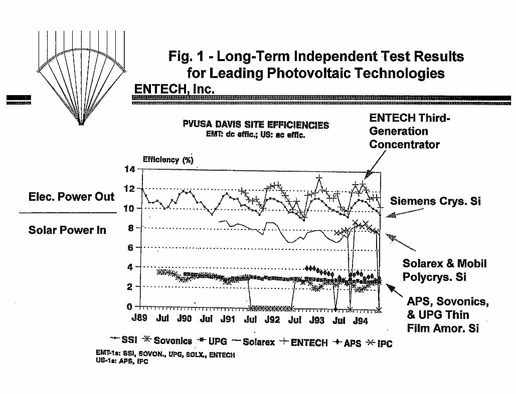
One of the third-generation systems was deployed in early 1991 at the PVUSA test site in Davis, California. This array has been independently tested side-by-side with other leading photovoltaic technologies in array sizes of at least 20 kW. Figure 1 shows the long-term results of this independent testing. The various technologies fall into four performance groups: thin-film amorphous silicon arrays are lowest at about 3% efficiency; polycrystalline silicon arrays are next at about 8% efficiency; crystalline silicon is the bighest of the one-sun arrays at about 10% efficiency; and the third- generation concentrator is the highest perfomer at about 11% efficiency.
In 1991, ENTECH won a Sandia contract under the Concentrator Initiative (CI) procurement. Under this CI contract, the ENTECH team initiated the design and development of a fourth-generation concentrator module. In 1991, ENTECH was also funded by NREL under the Photovoltaic Manufacturing Technology (PVMaT) Phase I procurement to define the manufacturing process for the new module. In 1992, ENTECH was funded by NREL under the PVMaT 2A procurement to develop and implement the manufacturing process for the new module. This report documents the work pexformed by the ENTECH team under this P W a T 2A program.
Two 100-kW power plants were deployed in 1995, using the newly developed module and the related mandacturing process. One plant is at the CSW Solar Park near Ft. Davis, Texas. The other plant is at TUE Energy Park in Dallas, Texas. Thus, the two largest utility companies in Texas are presently evaluating the new technology.
The following sections describe the new concentrator module, the key module manufacturing process improvements, and the impact of these improvements.
1

2.0 MODULE DESCRIPTION
Figure 2 shows a cross-sectional schematic of the fourth-generation concentrator module. There are four key functional elements in the module. The Fresnel lens gathers and focusses the direct portion of the available solar inadiance into a focal line. The solar cell packages are arranged along the focal line produced by the lens to convert the sunlight to electrical power. The heat sink convectively dissipates waste heat fiom the solar cell packages to the surrounding abosphere. The housing structure supports the lens and heat smk, and provides an environmental enclosure for the internal surfaces of the module. Module assembly is accomplished by snapping together six mating parts: the four sheet aluminum housing parts (two sidewalls and two endplates), the receiver assembly (one heat sink with cell packages attached), and the lens.
As further discussed in Section 3.0, the new fourth-generation module was designed by a team of orgmzations, including all of the suppliers of key parts. One of the first team design decisions for the fourth-generation module related to module size. To minimize parts count, the largest practical module size is preferred f?om both cost and reliability considerations. The lens aperture width limitation relates to the lens mandacturing process. Since 1978, Minnesota Mining and Manufacturing (3M) has produced the Fresnel lens for ENTECH, using the 3M-proprietary continuous Lensfilm process. In the early 1980's, the maximum prismatic pattern width for the Lensfilm process was 30 cm. By the late 1980'~~ this pattern width limitation was increased to 60 cm. By the early 1990'~~ the pattern width limitation was again increased to 100 cm. First-generation modules used four strips of LensfYm to form a lens with a 91-cm wide aperture. Second- and third-generation modules used two strips of Lensfilm to form a lens with a 91-cm aperture. For these earlier-generation lenses, the use of multiple strips of Lensfilm to form a lens resulted in substantial yield losses duringlamination of the 0.5 mm thick Lensfilm to 3.0 mm thick acrylic superstrate material. Thus, the decision was made to use a single strip of Lensfilm to form the fourth-generation lens. As further discussed in Section 5.1, this decision resulted in a new module aperture width of 85 cm, which is the chord width for the 100-cm wide prismatic pattern after arching into the final lens shape. The other key module size dimension is module length. Since 1978, Consumers, Inc., has produced the marine-grade aluminum housings for ENTECH. To form the sidewalls of the module housing, Consumers uses large presses with maximum length litnitations of 3.7 m. Thus, the decision was made to design the new housing at the upper end ofthis equipment limitation. This decision resulted in a new module aperture length of 366 cm. The new module aperture area is 3.1 sq.m., which is the largest photovoltaic module area of any type yet produced.
3


As further discussed in Section 5.3, solar cells for the new module are behg made by several leading one-sun module madactwing firms. Presently, most of these firms start their cell production process with 100 mm square wafers trimmed from 125 mm diameter silicon wafers. As further discussed in Section 5.3, this wafer size is well matched with the new lens size iftwo rectangular concentrator cells (about 50 mm total width by about 100 mm total lengfh) are cut from each square wder. Using such cells, 37 cell packages will fit end-to-end along the heat sink in the focal line produced by the lens. These cell packages are electrically interconnected in series to provide a module voltage slightly higher than most one-sun modules, which typically use 36 cells in series. As further discussed in Sections 5.4 and 5.6, each cell package incorporates a prismatic cell cover to eliminate gridhe obscuration losses and thereby boost cell performance. Each cell package also includes bypass diodes to protect the cell in case of shadowing.
As further discussed in Section 5.8, the cell packages are bonded to the heat sink using a proprietary new dry-fih process. The dry fih beneath the cell packages provides dielectric isolation between the cell circuit and the heat sink, as well as low themal resistance between these parts. The entire cell circuit is also encapsulated with a second dielectric film above the cell packages. The assembly of interconnected cell packages, dielectric layers, and heat sink is often called a photovoltaic receiver. The new photovoltaic receiver assembly approach is the subject of a pending U.S. Patent.
The heat sink beneath the cell packages is needed to reject the waste heat resulting from the incomplete conversion of the focussed sunlight into electrical power. Under peak irradiance conditions, about 2 kW per receiver of waste heat must be dissipated to the surrounding atmosphere by convection. The most cost-effective method of producing a large convective heat sink is by the aluminum extrusion process. Such an extruded heat sink was used on the third-generation concentrator module. However, the size of the third-generation heat sink was limited by available extrusion processes to a total fin area of about 1.7 sq.m. per meter of extruded heat sink length. In the early 199O's, this third-generation heat sink had the highest fin aredextruded length ratio yet achieved. For the fourth-generation heat smk, a new team member, Columbia Aluminum, was wiUing to attempt the extrusion of a new heat sink with twice the total fin area of the third-generation heat sink. As further discussed in Section 5.7, Columbia was successful in producing the new heat smk, which provides a phenomenal 3.4 sq.m. of fin area per meter of extruded heat sink length.
For the total heat sink length of 3.7 my the new heat sink provides 12.4 sq.m. of total fin area per module. This fh area is 4 times the aperture area of the module. The ratio
5

of heat transfer area to module aperture area is an important parameter in determining operating cell temperature, for either concentrator or one-sun modules. For a roof- mounted one-sun module, this ratio is about unity. For a game-mounted, exposed-back one-sun module, this ratio is about 2. Thus, compared to a roof-mounted one-sun module, the fourth-generation concentrator has 4 times as much heat transfer area per unit aperture area. Compared to a fiame-mounted one-sun module, the fourth- generation concentrator has 2 times as much heat transfer area per unit aperture area. With the new heat smk, the fourth-generation concentrator module has cell operating temperature levels much lower than for earlier generation concentrator modules. Indeed, side-by-side tests at both ENTECH and Sandia have confirmed that the cell operating temperature levels for the new concentrator are only 5-1 OC warmer than for fiame-mounted one-sun modules under most operating conditions.
As further discussed in Section 5.9, the electrical performance of the fourth-generation module is directly related to cell peIfomance. The lens provides 90% net optical efficiency at 21X geometric concentration ratio. The encapsulating layer above the cell package circuit provides a transmittance of 94%. The cell package packing factor on the heat sink is 98%. The product of these three factors times the cell efficiency equals the module efficiency. The power output of the module equals module efficiency times aperture area times available direct nonnal hadiance. Under standard test conditions (STC) of 1,000 W/sq.m. irradiance and 25C cell temperature, the module output is about 430 W with 17% efficient cells, or about 480 W with 19% efficient cells. In terms of aperture area (3.1 sq.m.) and power output, the new module is clearly the largest and most powerfd photovoltaic module of any type yet produced.
6
3.0 TEAM DEVELOPMENT APPROACH
At the outset of the development program, a team of experts w a ~ assembled to simultaneously design the new module and its production processes. This team includes all key component suppliers, independent mandacturing experts, government lab technical personnel, as well as ENTECH'S in-house technical sW. 'Key team members outside of ENTECH are identified in Table 1. 3M is the team member for optical components. Four of the leading silicon cell and one-sun module manufacturers fiom around the world are the team members for the concentrator cells and bypass diodes. The principal maker of solder-plated copper ribbon for the one-sun module industry is a team member. DuPont is the team member in the dielectric tape and film area. Consumers, Inc., continues to be the team member for module housings. Columbia is the heat sink team member. Two mandacturing technology h n s , AIT and nos, are also team members. Both National labs responsible for the Department of Energy's photovoltaic program are team members.
The team approach began at the brainstorming, conceptual design stage of the process and has continued through initial production and field deployment of the new module technology. Throughout, one key goal of the team approach has been to make maximum use of team members' existing production processes, rather than developing new in-house processes. A second key goal has been to incorporate continuous production processes instead of batch processes, wherever possible. Such continuous processes are obviously better equipped for high volume production at low cost than batch processes. A third key goal has been to minimjze the number of parts and the number of process steps required to make a module. A fourth key goal has been to relax allowable tolerances in module assembly, installation, and operation. The results of this team approach are described in the following sections.
7


4.0 NEW MODULE MA"ACTUlUNG PROCESS
Throughout this PVMaT program, the ENTECH team has worked to minimize both the number of parts in the new module and the number of process steps required to manufacture the new module. Figure 3 shows the new streamlined manufacturing process for the new module. Only three key sets of procured components and only three corresponding manufacturing processes are required to make the new module.
As M e r described in Section 5.4, four components must be procured to make cell packages: cells, bypass diodes, solder-plated copper ribbon, and prism cover tape. These components undergo four processes to yield complete cell packages: ribbon chopping, ribbon soldering, prism cover tape application, and flash testing for performance grouping.
As further described in Section 5.8, six additional components must be procured to make photovoltaic receivers: heat sinks, foam tape, dielectric tape, dielectric film, closeout shields, and end pieces. These components and the previously mentioned cell packages undergo eight processes to yield complete receivers: heat sink cleaning, foam tape application, dielectric tape application, cell package attachment, ribbon tab soldering, top dielectric film application (including closeout shields), end piece attachment, and receiver testing.
As previously described in Section 2.0, six additional components must be procured to make a complete concentrator module: aluminum housing kits, acrylic Fresnel lenses, lens gaskets, rotation interfaces, fasteners, and adhesives. These components and the previously mentioned receivers undergo four processes to yield complete modules: receiver positioning, housing kit attachment, lens attachment, and fastener attachment.
All of the procured components are mass-produced items. Most of these procured components are made by continuous processes (extrusion, embossing, roll-to-roll application, etc.), including the copper ribbon, the prism cover tape, the heat sinks, the foam and dielectric tapes, the dielectric film, the shields, the wire pigtail, the Fresnel lenses, the gaskets, and the structural adhesive tapes. All of the procured components can presently be produced at rates well above 10 MW/year.
All of the manufacturing processes for cell packages, receivers, and modules are simple and have been implemented with low-cost, easily replicated work stations. As furfher discussed in Section 6.0, an initial production run of about 200 kW was recently completed, without any work station duplication. During this initial run., single-shift
9


production rates of approximately 2.0 MW/year have been verified for all three key processes (cell package manufacture, receiver mandacture, and module manufacture). To produce cell packages at this rate, 8 people are presently needed (4 solderers, 1 prism cover applier, 1 flash tester, and 2 parts cleaner/suppliers). To produce receivers at this rate, 6 people are presently needed (2 tape/film appliers, 2 cell laydowners, and 2 solderer/testers). To assemble modules at this rate, 6 people are presently needed (1 parts cleaner/supplier, 1 caulker, and 4 assembly workers). Thus, a total production staff of about 20 people is presently needed to produce about 2 MWyear of concentrator modules. At a burdened labor rate of $2O/hour, this equates to about 40 cents per peak watt for the assembly labor cost content of the module.
Higher production rates can easily and quickly be reached by duplicating work stations and by implementing a second production shift. Ramp-up to a 10 MW/year production rate will require only a few months of lead time for work station duplication and production stajg training.
The following section discusses the key improvements, in both procured components and manufacturing processes, achieved under this PVMaT 2A program.
11

5.0 KEY IMPROVEMENTS UNDER THIS PROGRAM
5.1 New Fresnel Lenses
Two new versions of ENTECH's patented arched Fresnel lens line-focus optical concentrator have been designed, tooled, and produced. Figure 4 shows the basic design approach used by ENTECH to define a new lens. The same design approach has been successllly used for the past two decades on all previous generations of the arched lens. The shape of the lens is dictated by the symmetrical refiaction constraint used by ENTECH to maximize the lens optical efficiency and to minimize the effects of lens shape errors ( U S . Patent 4,069,812). This symmetrical refiaction constraint dictates that each solar ray passes through thelens symmetrically in terms of its angles of incidence and emergence at the two lens/& interfaces. At any location in the lens, the angle of incidence of a ray relative to the smooth outer lens surface is equal to the angle of emergence of the ray relative to the prismatic inner lens surface. While this condition defines the basic lens shape, it does not define the scale nor the rim angle (equivalent to F number) of the lens. The scale is selected to match the 3M Lensfilm process maximum prismatic pattern width. The rim angle is selected to maximize the concentration ratio in the presence of expected sun-pointing errors. For the fourth- generation module, both new versions of the lens provide the same focal length (73 cm), rim angle (40 degrees), and aperture width (85 cm). Both new lens versions are designed to focus sunlight onto a solar cell with an active width of 4.1 cm. Thus, the geometric concentration ratio for both versions is 21X (85 cd4.1 cm). The only difference between the two new lens versions relates to sun-pointing error tolerance. One version, designated Solar Concentrating Lensilm 1000 (SCL-1000) by 3M, is designed to accommodate up to 2 0.75 degree sun-pointing error levels with only a 10% drop in irradiance. The other version, designated SCL-3000 by 3M, is designed to accommodate up to 2 1.0 degree sun-pointing error levels.
For more than a decade, EN'IECH has successfully used the short-circuit current output of a scanning, 1 mm wide silicon cell to measure the photon flux profile across the focal plane of a Fresnel lens. Using this proven test, the focal plane irradiance profiles were scanned for both new lenses, with results shown in Figure 5. The net optical efficiency of the lens can be obtained by integrating under each of the two curves of Figure 5. For a 4.1 cm wide cell, this integration provides a net optical efficiency of 90% 5 1 % for both new lenses.
12


A second measurement of net optical efficiency was conducted by monitoring the short- circuit current output of a full-size cell with an active width of 4.1 cm. This test also provided a net optical efficiency measurement of 90% t 1%. This same full-size cell test setup was also used to measure the sun-pointing error tolerance of both new lenses, with normalized results shown in Figure 6. Note that the mild-focus SCL-1000 lens loses less than 10% of its on-track performance up to 0.8 degree sun-pointing errors. Similarly, the sharp-focus SCL-3000 lens loses less than 10% of its on-track performance up to 5 1 .O degree sun-pointing errors.
Lens/cell combinations for the previous generation of modules were designed to accommodate only 2 0.25 degree sun-pointing errors. Thus, the fourth-generation module is designed to accommodate 3 or 4 times larger sun-pointing errors than earlier modules, depending on the new lens version selection. This increased sun-pointing error tolerance clearly provides a more robust module and array.
The following section describes the new lens manufacturing process employed by 3M to make module-ready lenses.
15


5.2 New Lens Manufacturing Process
For prior generation lenses, ENTECH laminated the 0.5 mm 3M Lensfilm to 3.0 mm thick acrylic superstrate material to form a single-piece lens. For the fourth-generation lenses, 3M provides pre-laminated, module-ready lenses. ENTECH no longer has to maintain a lamination facility and no longer has to absorb the yield losses associated with this batch process. Furthermore, ENTECH no longer must worry about the environmental, safety, and health (ES&H) concerns associated with solvent lamination. Finally, module-ready lens prices fiom 3M are very reasonable. In 3 M W quantities, these lens prices are equivalent to about 30 cents per watt.
As part of this PVMaT 2A program, 3M developed a new continuous lamination process for joining the 3M LensfjJm to Rohm and Haas Implex extruded acrylic sheet. The Implex material is more impact resistant than normal acrylic sheet. Thus, while a 3.0 mm superstrate thickness is needed to survive 2.5 cm diameter hail ball impact at terminal velocity for normal acrylic, a lower thickness of Implex should,be equally strong. A lower thickness also enables the sheet to be coiled into a continuous roll, rather than being cut into individual flat sheets. Such a continuous superstrate roll makes a continuous lamination process feasible. Figure 7 shows a 3M-produced continuous roll of lens material comprising 0.5 mm Lensfilm laminated to 1.5 mm Implex via a solvent-fiee lamination process. This new continuous lens is superior to the previously used lens in terms of weight, cost, and shipping volume.
However, in early 1995, Sandia conducted a new set of simulated hail tests on a lens fiom the roll of Figure 7. This lens was damaged by 2.5 cm diameter ice balls impacting the lens at terminal velocity. Further tests and analysis are planned to determine if the 1.5 mm Implex thickness must be increased for hail survivability. While awaiting the results of these tests and analysis, ENTECH is presently using module-ready lenses from 3M, made in flat form with 3.0 mm extruded sheet sup erstrates .
17


5.3 New Solar Cells
ENTECHs fist- and second-generation modules used relatively expensive concentrator cells from Applied Solar Energy Corporation (ASEC). In the mid-1980'~~ ENTECH began to explore the use of one-sun type cells being made by one-sun module manuhcturers, including ARC0 Solar and Solarex. In the late 1980's and early 1990'~~ Solarex provided the cells for ENTECHs third-generation modules, including those for the 20 kW array at the PVUSA test site in Davis, California. In 1991, Sandia provided a separate Concentrator Initiative (CI) cell development contract to Solarex to develop the next generation of concentrator cell for ENTEcEFs fourth-generation module. Under this PVMaT 2A program, ENTECH also began working with three other cell suppliers, ME, BP Solar, and Siemens Solar. By 1993, all four cell suppliers were able to provide excellent cells for ENTECHs fourth-generation module.
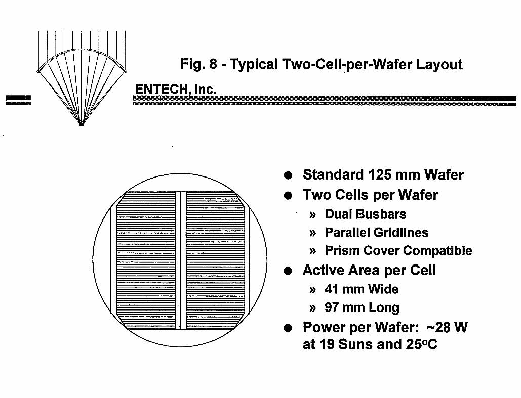
All four cell suppliers start with squared wafers cut fiom round silicon wafers, as shown in Figure 8. Two of ENTECH'S rectangular cells can be obtained Srom each squared wafer. Dual busbars are used on each cell to minimize gridhe resistance losses. Parallel gridlines are used to be compatible with ENTECHs prismatic cell cover, which is M e r discussed in Section 5.6. Beyond these similarities, the four cell suppliers use sigtdicantly different manufacturing processes. Solarex uses diamond saws to groove the cell to form buried fiont contacts. BP Solar uses lasers to groove the cell to form buried fiont contacts. ASE uses a shadow mask evaporation process to form the fiont contacts. Siemens uses screen-printed fiont contacts. The four firms are also at different stages in the development cycle of the concentrator cells. M E and BP Solar have both produced thousands of cells under commercial orders fiom ENTECH. Siemens has only produced sample quantities of cells for ENTECH, but has produced production quantities for another concentrator firm, SEACorp. Solarex has only produced sample quantities of cells for ENTECH, but has provided quotations for multi-Megawatt cell quantities for utility-scale applications.
In a normal one-sun module, a 100 mm square wafer would provide about 1.5 W of power. Ifthe one-sun cell manufacturer can produce the 100 mm square one-sun cell for $3 per watt, this equates to $4.5 per wder. In ENTECH'S module, this same wafer would provide about 28 W of power at an 18% cell efficiency. At $4.5 per wafer, this equates to 16 cents per watt for the cell cost in ENTECH'S concentrator module. Even if the extra gridlines and the two-cell separation required for the ENTECH concentrator cell were to cause the wafer price to double to $9, this still equates to only 32 cents per watt for the cell cost in ENTECH'S module. Thus, the marriage of one-sun type cells with ENTECH'S 21X concentrator provides a direct path to cost-effective silicon cells.
19

The measured perfbrmance levels of cells fiom all four suppliers are presented in Section 5.9. Integration of the cells into usable cell packages is discussed in the following section.
21
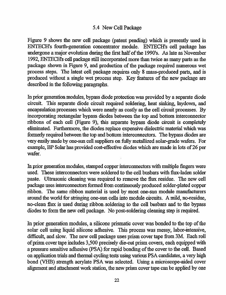
5.4 New Cell Package
Figure 9 shows the new cell package (patent pending) which is presently used in ENTECH's fourth-generation concentrator module. ENTECH'S cell package has undergone a major evolution during the first half of the 1990's. As late as November 1992, ENTECHs cell package still incorporated more than twice as many parts as the package shown in Figure 9, and production of the package required numerous wet process steps. The latest cell package requires only 8 mass-produced parts, and is produced without a single wet process step. Key features of the new package are described in the following paragraphs.
In prior generation modules, bypass diode protection was provided by a separate diode circuit. This separate diode circuit required soldering, heat sinking, laydown, and encapsulation processes which were nearly as costly as the cell circuit processes. By incorporating rectangular bypass diodes between the top and bottom interconnector ribbons of each cell (Figure 9), this separate bypass diode circuit is completely eliminated. Furthermore, the diodes replace expensive dielectric material which was formerly required between the top and bottom interconnectors. The bypass diodes are very easily made by one-sun cell suppliers on fully metallized solar-grade wafers. For example, BP Solar has provided cost-effective diodes which are made in lots of 26 per wafer.
In prior generation modules, stamped copper interconnectors with multiple fingers were used. These interconnectors were soldered to the cell busbars with flux-laden solder paste. Ultrasonic cleaning was required to remove the flux residue. The new cell package uses interconnectors formed fiom continuously produced solder-plated copper ribbon. The same ribbon material is used by most one-sun module manufacturers around the world for stringing one-sun cells into module circuits. A mild, no-residue, no-clean flux is used during ribbon.soldering to the cell busbars and to the bypass diodes to form the new cell package. No post-soldering cleaning step is required.
In prior generation modules, a silicone prismatic cover was bonded to the top of the solar cell using liquid silicone adhesive. This process was messy, labor-intensive, difficult, and slow. The new cell package uses prism cover tape fiom 3M. Each roll of prism cover tape includes 3,500 precisely die-cut prism covers, each equipped with a pressure sensitive adhesive (PSA) for rapid bonding of the cover to the cell. Based on application trials and t h e d cycling tests using various PSA candidates, a very high bond (VHB) strength acrylate PSA was selected. Using a microscope-aided cover alignment and attachment work station, the new prism cover tape can be applied by one
22


operator at rates faster than one cell per minute. Although this production step could be eventually automated, it is currently more cost effective to use a human operator.
In the early 1990 '~~ numerous attempts were made by the ENTECH technical team to incorporate dielectric protection and structural support into the cell package. One such attempt used alumina-loaded silicone both beneath the cell and above the interconnectors, all supported in an aluminum pan structure. An automated commercial potting machine was investigated in this effort. These attempts resulted in relatively cumbersome cell packages with numerous parts, which were difficult to interconnect and which had high levels of thermal resistance between the cell and heat sink. By abandoning these attempts to encapsulate the cell package as a unit, the entire package design has evolved into an elegantly simple assembly.
24

5.5 New Copper Ribbon Interconnectors
As discussed briefly in the last section, the new cell package uses 75 micron thick copper ribbon coated with 12 micron thick solder on both surfaces. As shown previously in Figure 9, the triangular shape of the ribbons allows two interconnectors to be chopped fiom each 10 cm long portion of 2.5 cm wide ribbon. The triangular shape is also well matched to the linearly increasing current level in the interconnector as it accumulates current fiom one end of the cell to the other end.
The new solder-plated ribbon with its self-contained solder costs 80% less than the previous-generation stamped interconnector and solder paste materials. In small quantity orders, the triangular ribbon interconnectors cost about a nickel apiece.
Figure 10 shows the work station which has been developed to cut the triangular pieces fiom a continuous reel of ribbon material. This small rule die chopper has already produced over 20,000 sets of interconnectors, verifying rates equivalent to 10 MW/year. For larger production rates, the chopper can be replicated for less than $20,000.
The ribbon material is very easy to use. A no-residue, no-clean flux is used to prepare the cell, diode, and ribbon surfaces for reflow-soldering. The re-flow process can be done manually with a soldering iron, or semi-automatically with a light-soldering work station. Figure 11 shows a Spire-manufactured light-soldering work station developed under this P W a T 2A project. While this Spire soldering station is capable of reflow-soldering a cell package every minute, the resultant package has residual stresses which cause problems during thermal cycling. In contrast, hand-soldered packages are very durable during thermal cycling. Thus, for ENTECHs present production process, hand-soldering is used to join the copper ribbon interconnectors to the cell and bypass diodes.
25


5.6 New Prism Cover Tape
Figure 12 shows a schematic of the new prism cover tape, which was developed under this PVMaT 2A program. The silicone prism cover optical elements are formed into the upper surface of the tape. The planar lower surface of the silicone prism cover is equipped with a pressure-sensitive adhesive (PSA). 3M makes the prism cover tape to ENTECH specifications (US. Patent No. 4,711,972). Each roll of prism cover tape contains 3,500 precisely die-cut prism covers. The PSA side of .the each cover is attached to a release liner in the same manner as a roll of labels for a laser printer. To protect and rigidize the silicone optical elements, each prism cover also has a removable liner on the optical element surface (not shown in Figure 12).
In Megawatt quantities, the new prism cover tape costs about 30 cents per cell. For typical production cells from ME, the prism cover tape increases the bare cell output of 8 W to about 14 W for the prism covered cell assembly. Thus the 6 extra watts of cell power cost about 5 cents each, for an enormous benefit to cost ratio.
To apply the cover to the cell, a prism cover alignment and application work station has been developed, as shown in Figure 13. The operator uses microscopic aids to look through the cover onto the cell before the PSA is allowed to contact the cell. The cover is moved in X-Y-Theta to align the optical elements to the gridlines, and the PSA is then pressed against the cell to form a strong, durable bond. The work station of Figure 13 has been used to apply more than 20,000 covers to cells. A operator can average rates faster than one cell covering per minute, using this work station. This rate is equivalent to about 2 MW/year for a single shift. For higher production rates, the work station can be replicated for less than $30,000.
28


5.7 New Heat Sink
The new heat sink was described in some detail in Section 2.0. Developed under this PVMaT 2A program, the aluminum eitrusion is made to ENTECH specifications by Columbia Aluminm. As shown in Figure 2, the heat sink includes 11 fins, each 15 cm long. The fins are tapered in thickness fiom the root to the tip, with an average thickness of about 2 mm. The fins are arranged in a star-burst .
radial pattem, which is very efficient from a thermal conduction viewpoint. A solid semi-circular bulb is formed at the base of the fins, with a flat top for cell package mounting. A 3.7 meter long heat sink weighs about 55 kg (120 pounds). In 1994, ENTECH purchased about 600 heat sinks for commercial orders at a price of about
' $1.25 per pound. Thus, the heat sink cost is equivalent to about 30 cents per watt of module output.
As previously described in Section 2;0, the new heat sink provides total fin area which is 4 times the module aperture area. This large ratio of heat dissipation area to energy collection area results in low cell operating temperature levels, even under the most adverse conditions (low wind, high kbient, high kradiance). Side-by-side tests at both ENTECH and Sandia have shown that the cell temperature level for the ENTECH concentrator module is only 5-1OC warmer than for fiame-mounted one- sun modules. Compared to the ENTECH third-generation concentrator modules at the PVUSA test site in Davis, California, the new heat sink provides more than twice the heat transfer area to aperture area ratio.
31

5.8 New Receiver Assembly Process
Figure 14 shows a photovoltaic receiver assembly, which consists of 37 series- connected cell packages mounted to one extruded heat sink. With materials help
. fiom DuPont, ENTECH has recently developed a proprietary new process (patent pending) for hssembling the photovoltaic receiver. This process involves fwo dry film processes to mount and encapsulate the cell package circuit. The first @-film process is used to mowit the cells to the heat smk, with a thin layer of TeEzel dielectric film between these parts. The second dry-& process is used to encapsulate the upper surface of the cell package circuit with another layer of Tefiel dielectric film. Both film processes are accomplished using commercially available tape and i3.m dispensing and application equipment fiom 3M. The dielectric isolation between the cell package circuit and the heat sink is excellent, as is the isolation between the cell package ;circuit and the surrounding atmosphere. The thermal resistance between the cell packages and the heat sink is very low, resulting in only a 10-13 C cell-to-heat sink temperature difference hder peak irradiance conditions as confirmed by Sandia. The new receiver assembly process has eliminated more than 300 parts per receiver compared to the previous receiver assembly process. The elimination of all wet silicone layers in the receiver assembly process has been a joyfiil experience at ENTECH. The details of the new process will not be made public until the pending U.S. patent is approved and published. However, ENTECH is pleased to report that the new process is simple, streamlined, and rapid, with sigmficant quality advantages and cost savings.
ci
32

5.9 Cell and Module Performance
Figure 15 shows the relationship between module efficiency and cell efficiency for the fourth-generation concentrator. The measured lens optical efficiency is 90%. The measured Tefiel encapsulating layer transmittance is 94%. The cell package to receiver packing factor is 98% (i.e., the total active length of all 37 cells is 98% of the lens aperture length). The product of these three factors times cell efficiency equals module efficiency. With 17% cells, the module efficiency is about 14%. . With 19% cells, the module efficiency is about 16%. With 22% cells, the module efficiency is about 18%.
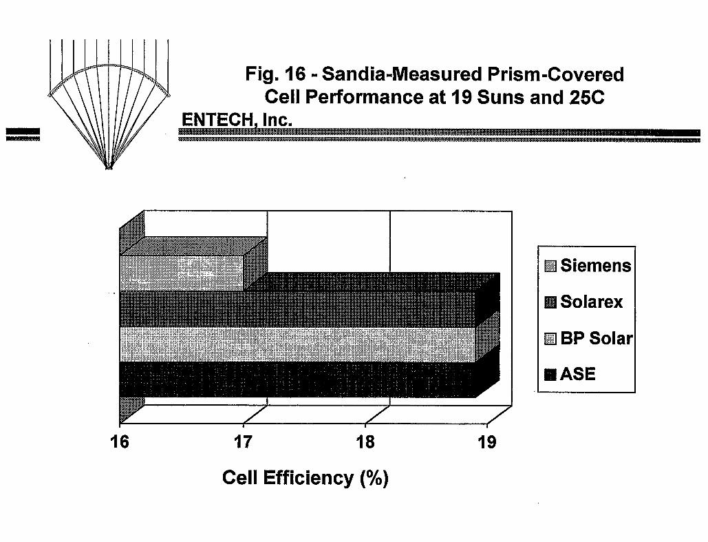
Figure 16 shows the present status of cell efficiency for the four cell suppliers. Solarex, BP Solar, and ASE have delivered cells which have been independently measured by Sandia to be 18.9% efficient at 19 suns irradiance (AM1.5D spectrum) and 25C cell temperature. Siemens has delivered cells which have been measured by Sandia to be 17% efficient under the same conditions. All cells were tested in cell packages, including prismatic cell covers and copper ribbon interconnectors, as described in Section 5.4.
The data of Figure 16 don't teu the wholestory of cell efficiency. These cells are representative of&e best-performing cells from all four suppliers. A more meaningfid pefiormance index is the lot-average cell efficiency for a large production run of cells. ENTECH has just completed two 100-kW module production runs, using over 20,000 cells from ME. The lot-average efficiency of the cell packages produced with these cell is slightly over 17% at 19 suns irradiance and 25C cell temperature.
The measured outdoor performance for two modules using these production cells is shown in Figure 17. Both modules used mild-focus SCL-1000 lenses fiom 3M, as described in Section 5.1. Two different lens thicknesses were utilized, with no impact on module performance. One of the lenses used 3.0 mm thick ordinary extruded acrylic superstrate, while the other lens used 1.5 mm thick Rohm and Haas Implex superstrate, as further discussed in Section 5.2. Note that the operational power output of each module was just under 400 W at irradiance levels of 920-940 W/sq.m. and an ambient air temperature of 5C. Smdia later tested both modules very thoroufly, and rated each at about 430 W at standard test conditions (STC) of 1,000 W/sq.m. direct irradiance and 25C cell temperature. Since the module has an aperture area of 3.1 sq.m., this 430 W power level equates to a module efficiency of about 14%, in close agreement Miith the data of Figure 15 for 17% efficient cells.
34


6.0 PROCESS VERIFICATION VLA INITIAL RUN
During 1994, ENTECH produced about 600 modules to fdiU commercial orders for two 100 kW utility-scale photovoltaic power plants. This initial run of fourth- generation modules allowed the ENTECH production team to verify the new manufacturing processes for both procured components and assembly operations. The following two sections briefly describe the two systems. Section 6.3 then describes smaller systems which are also being produced using the new mandacturing technology developed under this PVMaT 2A program.
6.1 TUE Energy Park 100-kW System
Figure 18 shows the first SolarRow large array of ENTECHs fourth-generation concentrator modules installed at TUE Energy Park in Dallas, Texas, in November 1994. The SolarRow is believed to be the world's largest two-axis photovoltaic sun- tracker. The SolarRow contains 72 modules with a total aperture area of 220 sq.m. and a total operational power output of about 25 kW. Four such SolarRows are now installed and operational at TUE Energy Park. The system was dedicated on March 8,1995. On the morning of the dedication, the system was providing 95 kW of AC power to the TUE grid. The system includes 288 concentrator modules, manufactured using the components and processes described in the previous sections of this report.
6.2 CSW Solar Park 100-kW System
Figure 19 shows one of four SolarRows installed at CSW Solar Park in Ft. Davis, Texas. Each row is over 100 meters long in the east-west direction, and represents a unitized steel structure. The structure tilts fiom north-to-south via shafts and bearings on 13 posts. The 72 modules mounted in the SolarRow fiame roll fiom east-to-west in Venetian blind fashion via shafts and bearings on both ends of each module. The system has been operational since January 14,1995. The system includes 288 concentrator modules, mandactured using the components and processes described in the previous sections of this report.
The measured power output for each of the four SolarRows, under typical operating conditions, is provided in Figs. 20 and 21. Note that each row provided 24-26 kW of power output under the operational conditions at the time of the test. During February 1995, the system was observed while providing 102 kW of AC power to the CSW grid.
39


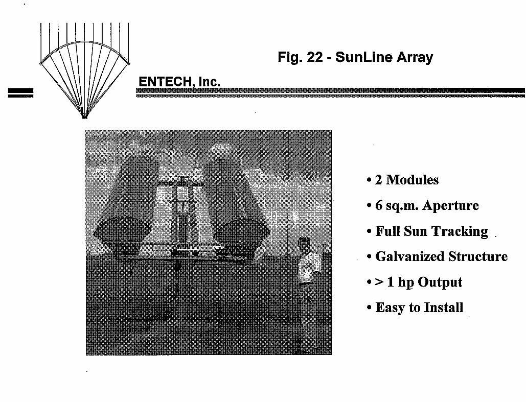
6.3 SunLine Small Arrays
Figure 22 shows a two-module small may, called S d i n e by ENTECH. ENTECH has just begun to commercialize the S d i n e array, which uses exactly the same module as the large utility-scale SolarRow arrays described in the last two sections. Thus, the S d i n e modules use the manufacturing technology described in the previous sections of this report.
In summary, via initial production runs, ENTECH has successfully verified the mandacturing technology developed under this PVMaT 2A program. ENTECH is presently applying this P W a T technology to both large arrays (SolarRow) and to small arrays (Sdine).
44

7.0 IMPACT OF THE IMPROVEMENTS
7.1 Module Manufacturing Cost vs. Production Rate
ENTECH'S fourth-generation concentrator module manufacturing cost includes the purchased component costs (the lens from 3M, the cells from one of four suppliers, the heat sink from Columbia, the module housing from Consumers, and several small items) and the module assembly costs. Table 2 summarizes these cost elements for three different annual.production rates, 100 kW, 3 MW, and 30 M W , respectively .
The purchased component costs are well known and are strong functions of annual production volume. The assembly costs are relatively low, largely due to the streamlined production processes developed under this P W T 2A program. As discussed in Section 4.0, a production staff of about 20 people can produce approximately 2 MWyear of modules. However, at present intermittent ENTECH production rates of 100-200 kW/year, stafftraining, line'star-up, and line shut- down efforts essentially double the assembly costs, compared to a continuous production level of 2-3 MW/year. At. still higher production rates, the labor cost content will continueto decline slowly, due to added automation and normal learning curve trends.
The total direct manufacturing cost for the concentrator module is about $3.30/W at 100 kW/year, $1.80/W at 3 MW/year, &d $1.20/W at 30 MW/year. Compared to one-sunphotovoltaic modules, these costs range from barely competitive at 100 kW/year to dramatically better at 3 MW/year. This situation is not diffiicult to understand, since many one-sun module manufacturers have already reached production rates of 5-20 MW/year. At a similar production rate, the concentrator module production cost is at least 70% lower than the one-sun module production cost.
The following section presents the system costs and energy economics that correspond to the module production costs discussed above.
46


7.2 System Costs and Energy Economics
The lowest curve in Figure 23 shows the module manufacturing cost versus annual production rate, taken directly from Table 2 'above. Note that at 10 Mw/year, the module manufacturing cost is about $1.50 per watt. The balance of systems @OS) costs include the SolarRow structure, the sumtracking drives and controls, the foundatioiis, Wiring, and the power conditioning system (inverter). For ENTECH'S technology, these BOS costs are slightly less than the module costs. The middle curve in Figure 23 includes module costs plus BOS costs. The highest curve in Figure 23 includes module costs plus BOS costs plus a 25% gross profit margin on both. This curve is equivalent to an installed system price. Note that this price falls below $3 per watt at 10 MW/year production rate.
The energy cost for such systems depends on two additional factors: the system annual capacity factor (at least 21% for a high insolation location like Phoenix, Albuquerque, Barstow, etc.) and the owner's annual fixed charge rate on capital investments. The fixed charge rate depends on many factors, including the owner's sources of funds, tax situation, etc. Energy cost curves for two representative values of the fixed charge rate, 5% and lo%, are shown in Figure 24. These two curves present the levelized energy cost corresponding to the system prices of Figure 23. For example, at 10 MWyear production rate, the system price is about $3 per watt. For a 5% fixed charge rate, this system price provides electricity at a levelized price of 8.5 cents per kwh. For a 10% fixed charge rate, this system price provides electricity at a levelized price of 17 cents per kwh. At higher production rates, these levelized electricity prices continue to fall to lower levels.
These energy prices are substantially lower than for present photovoltaic systems of any kind, including those being manufactured at rates well above 10 MWyear. Furtherthore, these eneru prices can be obtained without any breakthroughs in materials, mandacturing processes, stability, or efficiency. Thus, the fourth- generationconcentrator technology described in this report provides a clear and direct path to much lower electricity prices for photovoltaic systems. Indeed, the near-term electricity prices for this technology are comparable to conventional residential electricity rates in several parts of the U.S. today. What is needed is a sustainable larger annual volume of system production and sales. With the manufaccturhg technology improvements made under this PvMaT 2A program, ENTECH is now ready to make a sigm€icant contribution to the power needs of people living m the sunny regions of the world.
48


8.0 REFERENCES
1. M. J. O'Neill et al., "Photovoltaic Mandacturing Technology Improvements for ENTECH'S Concentrator Module: Phase 1 Final Technical Report," NREL/TP- 214-4486, Denver, November 1991.
2. M.J. O'Neill et al., " ~ C H ' s Fourth-Generation Linear Concentrator Module," 1992 DOE/Sandia Crystalline Photovoltaic Technology Project Review Meeting, SAND92-1454, Albuquerque, July 1992.
3. T.M. Bruton et al.; "Recent Developments in Concentrator Cells and Modules Using Silicon Laser Grooved Buried Grid Cells," 1 lth European PVSEC, Montreaux, Switzerland, October 1992.
4. M. J. ONeill, "Fourth-Generation, Line-Focus, Fresnel Lens Photovoltaic Concentrator," 4th Sunshine on Crystalline Silicon Solar Cells, Tokyo, Japan, November 1992.
5. M. J. O'Neill and A. J. McDanal, "Manufacturing Technology Improvements for a Line-Focus Concentrator Module," 23rd IEEE-PVSC, Louisville, May 1993.
6. M. J. O'Neill, "Photovoltaic Mandacturing Technology (PVMaT) Improvements for ENTECHs Concentrator Module," 12th NREL PV Program Review Meeting, Denver, October 1993.
7. M. J. O'Neill and A. J. McDanal, "Fourth-Generation Concentrator System: From the Lab to the Factory to the Field," 1st WCPEC, Hawaii, December 1994.
51
APPENDIX A - SELECTED PILOT RUN MANUFACTURING DATA
In the final year of this PVMaT2A project, ENTECH produced approximately 600 concentrator modules for two utility-scale power plants. Each of these power plants has a design rating of 100 kW. The fist of these two plants was deployed at CSW Solar Park near Ft. Davis, Texas, with inverter startup in J a n w , 1995. The second plant was deployed at TU Electric Energy Park in Dallas, Texas, with inverter startup in February, 1995. The modules for these two plants were produced at ENTECH using the PVMaT-developed mandacturing process for the first time. Production line startup, debugging, and data collection activities were included in this PVMaT2A project. This appendix provides key mandacturing data related to the pilot production run of 600 concentrator modules.
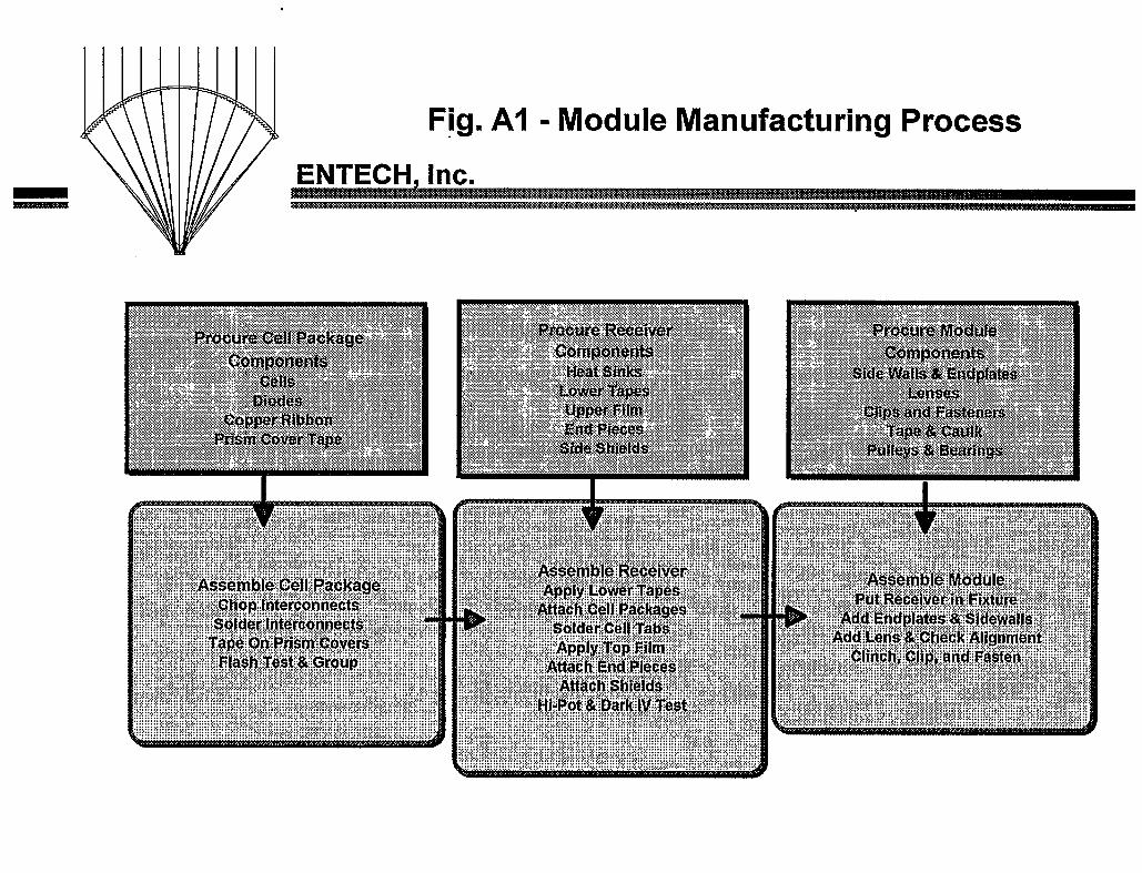
Figure A1 summarizes the new production process for ENTECH'S fourth-generation module. ENTECH procures dl key components from suppliers who have been involved in the design, development, and implementation of the new module manufacturing process. Procurement and assembly processes are divided into three elements: the cell package, the receiver, and the module. These elements have been m y descried in the main body of this report. Thirty-seven cell packages are used in each receiver. One receiver, one lens, and one housing kit are used in each module. The following paragraphs present data related to the cell package, receiver, and module production for the two utility power plants discussed above.
The cell packages were assembled by a small crew, consisting of 4 solderers, 1 prism coverer, 1 flash tester, and 2 materials suppliers. Figure A2 shows the cell package completions for a 48-day period. The bottleneck in the production process was the flash testing station, which required fiequent recaliiration and repair. Note that 12,000 cell packages were completed during this period, for an average daily output of about 248 units. Peak rates were much higher than this average rate. For example, the solderers and the prism coverer were routinely able to complete 1 cell package per minute.
Cell package yield losses were sigmficant during the pilot production run. Figure A3 shows the actual losses by category. Four of the five categories relate to cell breakage. Small cracks in the cells are difficult to see with the naked eye. Thus, the exact location where the break occurs is hard to determine. The location where the cell is found to be broken is easier to quanbfy, as shown in the figure. The prism coverer has an advantage in iden-g cracked cells. The cell is placed on a vacuum chuck for prism covering. Ifthe cell is cracked, the vacuum does not holddhe cell in place.
Appendix A - Page 1


Thus, the larger percentage of cell found broken by the prism coverer does not mean that these cells were broken in the prism covering process; indeed, most of these cells were broken during previous handling steps. Total cell breakage losses amounted to about 4% of cell package starts. An additional 2% of the cell packages were not used because their measured performance was less than 16% electrical conversion efficiency at 19 suns irradiance and 25C cell temperature. Total yield losses were therefore just under 6%. Much of the breakage loss occurred during on-the-job training of employees. Therefore, for future production runs, employee experience should reduce the total cell package yield losses to less than 5%.
The best measure of cell package quality is conversion efficiency. Figure A4 shows the daily average cell package efficiency for the same period of 48 production days. Note that the average is relatively constant, within the probable error of the efficiency measurement. This consistent value of cell package efficiency indicates a relatively robust process. Figure A5 shows the performance histogram for over 20,000 cell packages produced during the pilot production run. Note that the lot-average cell package efficiency is over 17%. Note also that nearly all of the cell packages had efficiency levels of 17.1% t 1%. This tight quality grouping is also characteristic of a robust process.
Completed cell packages were grouped by performance and then assembled into photovoltaic receivers by a relatively small crew, consisting of 2 tape/& appliers, 2 cell package bonders, and 2 solderer/testers. While peak daily rates reached 16 receivers per day, average rates were about 9 receivers per day, as shown in Figure A6. Unlike cell packages, receiver yield losses were essentially zero. If a cell were broken or Med electrical testing during assembly into a receiver, it was removed and replaced. Each receiver was tested for electrical performance by passing 25 amps of DC current through the unit in both directions while measuring the DC voltage at the receiver terminals. This test verified the continuity and impedance of both the cell circuit and the bypass diode circuit. In addition, a 2,200 V hi-pot cell-to-heat sink dielectric test was also performed on all receivers produced. The results of these electrical tests were extremely consistent on all 600 receivers produced during the pilot run, verifjrlng the robustness of the receiver manufacturing process.
Each completed receiver was integrated into a module by snapping it together with one lens, two endplates, and two sidewalls. Module assembly was performed by a small crew of 4-6 people. Figure A7 shows the module completion curve for a four-week period, including the Thanksgiving holiday. Three shipments of 27 modules each were watched each week fiom ENTECH to complete the CSW Solar Park 100 kW power
Appendix A - Page 5


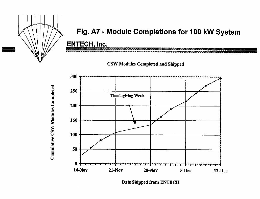

plant. Since Sandia has rated these modules at 430 Watts each, this 81 module per week rate is equivalent to about 2 MW/year of photovoltaic module production.
The best measure of module quality is power production in the field. Figure A8 shows the measured performance of 288 modules installed in four rows at the CSW Solar Park in West Texas. Each row contains 72 modules grouped into three source circuits. At the end of each row, the three source circuits are connected in pardel, with two Wires leaving each row on their way to the inverter. Each such row is called a SolarRow by ENTECH. The measured IV curve of each of the four SolarRows at CSW Solar Park is provided in Figure A8. Note that each row produced 25 kW t 1 kW during the test, which was conducted under less than peak hadiance conditions. The consistent shape of the four SolarRow IV curves indicates that the modules provide consistent power outputs, further venfjung the quality of the modules and robustness of the manufacturing process.
Appendix A - Page 10


APPENDIX B - ES&H IMPLEMENTATION ON THE PRODUCTION LINE
Under the PVMaT2A program, ENTECH initiated the implementation of a comprehensive environmental, safety and health (ES&H) plan to assure that all manufacturing processes are in compliance with OSHA standards. The “OSHA Compliance Guide” provided the basic resources necessary to hitiate an ES&H plan. These resources included: General Safety Standards, Sample Programs and OSHA forms for record-keeping, posting and reporting requirements. The overall goal of the ES&H plan is to provide policies, procedures, and practices that protect the environment as well as- protect employees fi-om safety and health hazards.
The following ES&H programs are currently in place and are under continuous review:
Accident Prevention Plan
Hazard Communication Program
Fire Safety Program
Drug-Free Workplace Policy
In the following paragraphs, each of the programs listed above will be summarized in greater detail.
ACCIDENT PREVENTION PLAN - The primary objective of this plan is to provide a safe and healthy working environment for all ENTECH employees. The plan contains a policy statement fkom ENTECH management accepting responsibility for leadership in the program and encouraging all employees to be safety-conscious. The company safety officer and his assistant are specified by name and their respective responsibilities and authority for enforcement are delineated. The plan provides provision for annual review, desmies documentation requirements, employee training, accident investigation, internal audit and inspection, training and orientation of new employees.
l3AZARDS COMMUNICATION PROGRAM - This program was implemented in compliance with the Code of Federal Regulations (CFR), 29 CFR 1910.1200. The program provides for: the proper labeling of all containers of hazardous chemicals; the location of and explanation of material safety data sheets (MSDS); employee training
Appendix B - Page 1

and information; an updated list of hazardous chemicals used at ENTECH; special precautions to follow for non-routine tasks; and procedures for outside contractors.
FIRE SAFETY PROGRAM - This program meets the OSHA requirement for a written program in 29 CFR 1910.38. The person responsible for canying out this program as well as his responsibilities and authority are specified. The program includes: building Ere exit inspections; portable Ere extinguisher rules; emergency evacuation plan procedures; fire prevention plan; and a f ie suppression system.
DRUGF’REE WORKPLACE POLICY - Company policy related to alcohol and controlled substances is stated. Company rules and disciplinary action in the event of rules violation are described. AU employees are required to sign a statement stating they have read the policy and that they agree to abide by the policy.
A written copy of each of the programs descriied above is available to employees upon request. Material safety data sheets for chemicals used in the workplace are filed together and are available to all employees. Documentation including “Sdety Hazard Reports” and “Log and Summary of Occupational Injuries and Illnesses” are maintained for review by employees.
Each ENTECH employee in a supervisory position views safety videos supplied through the Texas Workers’ Compensation Insurance Fund’s Safety Video Library. Safety videos include Supervisor Responsibility, How to Develop a Safety Program, Hazard Communication - An Overview, Housekeeping on the Job Site, and How to Conduct a Safety Meeting. These same individuals participated in a safety meeting entitled What to Do When a Spill Occurs. Attack Pac emergency spiU kits are located throughout the facility to assist in cleanup and containment of minor chemical spills, in the event one occurs. Additionally, first-aid kits, emergency eye wash kits, and an emergency shower are located in convenient spots throughout the facility.
In terms of environmental issues, ENTECH is classified as a “Conditionally Exempt Small-Quantity Generator.” As such, ENTECH can store, for an indefjhite time period, waste materials up to 1,000 kg on the premises. Toxic chemicals, flammable liquids, and hazardous wastes are properly stored in a metal flammable liquid storage cabinet. When required, iims that specialize in waste chposal will be called to dispose of these materials properly.
Appendix B - Page 2

ENTECH'S fourth-generation module manufactwing process was shown schematically in Appendix A, Figure Al. The ES&H programs discussed above were implemented under the PVMaT2A program and were verified on the production run discussed in Appendix A. Specific ES&H improvements for the three primary manufacturing steps (cell package, receiver and module manufacture) are described below.
ES&H improvements implemented in the cellpackage manufacctutingprocess include:
Solder paste and caustic fluxes were eliminated in favor of solder-plated copper ribbon and mild, no-residue, no-clean flux.
All soldering operations were performed in a large room with a large exhaust system. The ventilation system quickly removes harsh vapors generated during the soldering process. Masks and small personal fans were also available.
rn Safety glasses and gloves were required during all process steps.
rn To prevent injuries due to fatigue or due to performing the same movements repeatedly, breaks were increased fiom two 15-minute breaks to four 10-minute breaks spaced evenly throughout the day.
Employee training specifically for cell soldering included a three step process. The employee was asked to read and study a detailed process specification (attached hereto). Each employee viewed a video in which every step in the process was performed by a highly trained technician. Finally, the employee was allowed to perform the soldering operation under the supervision of a trained supervisor.
The prism cover application work station was designed with a built-in safety feature that prevented the operator fiom being injured by moving parts. To prevent injuries and relieve fatigue due to repetitive movements, thumb buttons were replaced by oversized palm buttons to operate the work station.
ES&H improvements implemented in the receiver manufactwingprocess include:
1 Back braces were worn by production workers anytime receivers were required to be lifted. Receivers were moved fiom station to station on specially fabricated roll-around tables.
Appendix B - Page 3
H
H
H
H
H
Mild, biodegradable degreasers were used to clean bare aluminum extrusions.
As in the cell package process, no-residue, no-clean flux was used to solder the solder-plated interconnects f?om cell to cell. Vapors generated during this process step were removed via a ventilation/exhaust system.
Messy two-part mixtures of RTV and alumina were eliminated in favor of clean, simple VHB t a p e s l h below and above the cell packages.
Each receiver was subjected to standard hi-pot testing and dark IV testing with a power supplF Electrical leads were well marked with tags to prevent improper hook-up or electrical shock. ,
Safety glasses, gloves, lab coats and hair nets are required during all process steps.
ES&H improvements implemented during the m h l e manufaccturingprocess include:
H The specially-fabricated roll-around tables are used to move receivers to the module assembly fixture.
Back braces are worn to prevent back injuries when lifting receivers or handling modules.
Lifting aids are used to raise/install the Fresnel lens on the module.
Lifting aids, roll-around tables and dollies are used to move the completely assembled module to the shipping dock.
Safety glasses are required during all process steps.
H
H
H
1
Appendix B - Page 4

.
PHOTOVOLTAIC CELL SOLDERING PROCESS SPEClFlCATION ENTECH Drawing No. 14005
MATERIAL REQUIRED Photovoltaic Cell (Dwg. No. 18006) Two Diodes (Dwg. No. 18007) Multicore X32-1Om No Residue Flux Multicore lTC1 Tip TinnerCleaner Two Back Interconnects (Dwg. No. 18005-01) Two Front Interconnects (Dwg. No. 18005-2) Cotton Gloves Cotton Tip Applicators
EQUIPMENT REQUIRED 100 Watt Soldering Iron (Weller, W1 OOPG) Soldering Stand (Weller, PHI 00) Solder tip (Weller, CT6D7) Two Solder Fixtures (Dwg. No. 18003) Voltmeter Halogen Lamp (20 Watt Bulb) Safety Glasses Cell Assembly Drawing (Dwg. No. 18000)
PROCEDURE
1.
2.
3.
Position the cell in the solder fixture with the active cell area (dark side) facing up. Position both diodes in the solder fixture with the side marked "N" (negative polarity) facing down and the "N"-mark on the end nearest you. NOTE: Because. the cell.and diode are extremely fragile, handle very carefully to prevent breakage.
With a cotton tip swab flux the busbar on each side of the cell and flux the exposed surface of both diodes.
Since front interconnects will be soldered to the cell busbar and to the diode on both sides of the cell, flux the entire surface of both interconnects on the side to be soldered. Check to make sure that all parts to be soldered have been fluxed.

4.
5.
6.
7.
a.
9.
10.
11.
12.
Place a front interconnect in the fixture, fluxed side down. Push the blunt end of the interconnect toward the fixture and push out along the diagonal edge to properly position the interconnect in the fixture. The interconnect should not extend into the active cell area. A small area between the interconnect and the inner edge of the busbar (adjacent to the cell active area) should be visible.
With a slow and deliberate motion of the soldering iron, solder the interconnect to the cell busbar. Solder by moving the soldering iron in a smooth, continuous motion toward you. Use the positioning tool to hold the parts in place. NOTE: When soldering, the soldering iron tip is always pointed away from the cell active area. While holding the parts in place with the positioning tool, solder the interconnect to the diode. Solder by moving the soldering iron in a slow continuous motion away from you.
Rotate the fixture 180 degrees and place the second front interconnect in the fixture. Push the blunt end of the interconnect toward the fixture and push out along the diagonal edge for proper positioning. The interconnect should not extend into the active cell area. A small area between the interconnect and the inner edge of the busbar (adjacent to the cell active area) should be visible. Check for proper positioning.
As in Step 5, solder the interconnect to the cell busbar by moving the soldering iron in a slow continuous motion toward you. The parts are held in place with the positioning tool. Solder the interconnect to the diode by moving the soldering iron in a slow continuous motion away from you.
By gently rubbing with your finger, check to see if there a re any sharp points on the front of the cell at any place solder has been reflowed. If any sharp points are found, carefully smooth out with the soldering iron. This completes the soldering process on the front side of the cell. Remove the cell assembly from the fixture. Turn the assembly over and position the assembly in the second soldering fixture.
Flux the exposed surface of the two diodes. Flux the back of the cell along both long edges. An area about 1/4 inch wide along the entire length of the cell is sufficient.
Flux the entire surface of both back interconnects on the side to be soldered.
Place a back interconnect in the fixture, fluxed side down. Push the blunt end of the interconnect toward the fixture and push out along the diagonal edge to properfy position the interconnect in the fixture. Check to make sure that the interconnect does not extend too far out on the back of the cell. The edge of the interconnect should be parallel to the edge of the cell and no more than 0.12 inches from it.
Repeat Step 5

13. Rotate the fixture 180 degrees and place the second back interconnect in the fixture as described in Step 11.
14. Repeat Step 5.
15. By gently rubbing with your finger, check to see if there are any sharp points on the back of the cell at any place solder has been reflowed. If any sharp points a r e found, carefully smooth out with the soldering iron. This completes the soldering process.
16. Remove the finished soldered cell assembly from the fixture.
17. Perform a voltage check on the cell under illumination to make sure the cell is not shorted top-to-bottom. Position the cell under the lamp with the light on the active cell area. With one probe on the back interconnect and the other probe on the front interconnect on the opposite side of the cell, measure the cell output voltage under illumination. The output voltage will vary from cell to cell but should always be within 0.35 to 0.55 volts. A cell assembly with a output voltage outside this range should be set aside for further evaluation.
18. The fully soldered cell assembly should be dimensionally consistent with the cell assembly shown in ENTECH Drawing No. 18000,

Form Approved OMB NO. 0704-0188 REPORT DOCUMENTATION PAGE
J
1. AGENCY USE ONLY (Leave blank)
4.TlTLE AND SUBTITLE
Photovoltaic Manufacturing Technology (PVMaT) Improvements for ENTECH's Concentrator Module
6. AUMOR(S)
M. J. ONeill and A. J. McDanal
7. PERFORMING ORGANIZATION NAME(S) AND ADDRESS(ES)
ENTECH, Inc. P.O. Box 61 2246 (1 01 5 Royal Lane) DFW Airport, TX 75261 -2246
2. REPORT DATE 3. REPORT TYPE AND DATES COVERED October 1995 Final Subcontract Report, 17 February 1992 - 14 June 1995
9. SPONSORlNG/MONlTORlNG AGENCY NAME@) AND ADDRESS(ES)
National Renewable Energy Laboratory 1617 Cole Bhrd. Golden, CO 80401 -3393
17. SECURITY CLASSIFICATION OF REPORT Unclassified
11. SUPPLEMENTARY NOTES
NREL Technical Monitor: R. Mitchell 1 2 a DISTRIBUTION/AVAILABlLlTY STATEMENT
18. SECURITY CLASSIFICATION 19. SECURITY CLASSIFICATION OF THIS PAGE OF ABSTRACT Unclassified Unclassified
~~ ~~ ~
5. FUNDING NUMBERS
C: ZM-2-11040-4
TA: PV650101
8. PERFbRMING ORGANIZATION REPORT NUMBER
10. SPONSORING/MONlTORING AGENCY REPORT NUMBER
TP-411-20277
DE96000478
1%. DISTRIBUTION CODE
UC-1270
~~ ~~ ~
13. ABSTRACT (Marimurn 200 words)
Since 1978, the ENTECH technical team has been developing, field testing, refining, and commercializing photovoltaic concentrator systems based on a patented arched Fresnel lens optical concentrator, which provides maximum optical efficiency coupled with exceptional real-world error tolerance. First- through third-generation systems were deployed from the early 1980s to the early 1990s. In 1991, ENTECH was awarded a contract by Sandia National Laboratories to develop afourthgeneration concentrator module. In 1992, ENTECH was funded by NREL under the PVMaT Phase 2A procurement to develop and implement the manufacturing process for the new module. This report documents the work performed by ENTECH, Inc. under this PVMaT Phase 2A program.
14. SUBJECT TERMS
photovoltaics ; solar cells ; concentrator module ; ENTECH ; PVMaT; manufacturing
15. NUMBER OF PAGES 73
16. PRICE CODE
20. LIMITATION OF ABSTRACT
I I1
N S N 7540-01-280-5500 Standard Form 298 (Rev. 2-89) Prescribed by ANSI Std. 239-1
298-1 0