PHOTONIC PROCESSING OF ULTRA-BROADBAND RADIO …
146
PHOTONIC PROCESSING OF ULTRA-BROADBAND RADIO FREQUENCY WAVEFORMS A Dissertation Submitted to the Faculty of Purdue University by Ehsan Hamidi In Partial Fulfillment of the Requirements for the Degree of Doctor of Philosophy December 2010 Purdue University West Lafayette, Indiana
Transcript of PHOTONIC PROCESSING OF ULTRA-BROADBAND RADIO …
PHOTONIC PROCESSING OF ULTRA-BROADBAND RADIO FREQUENCY
WAVEFORMS
A Dissertation
Submitted to the Faculty
of
Purdue University
by
Ehsan Hamidi
In Partial Fulfillment of the
Requirements for the Degree
of
Doctor of Philosophy
December 2010
Purdue University
West Lafayette, Indiana

ii
To my mother Shahnaz Hamidi and my father Esmaeil Hamidi.

iii
ACKNOWLEDGMENTS
I would like to thank my advisor Professor Andrew M. Weiner for his guidance,
support, and patience throughout my graduate study. It was a great opportunity to be a
member of his group to learn and do research. I also would like to thank Professor Mark
R. Bell, Professor Demitrios Peroulis, and Professor Vladimir M. Shalaev for serving as
my Ph.D. committee members and for their helpful comments.
My special thanks go to our group research engineer Dr. Daniel E. Leaird for his
invaluable technical support and many fruitful discussions. I would like to thank my
colleague V. R. Supradeepa, and my former colleagues Dr. Ingrid S. Lin, Dr. Shijun Xiao,
and specially Dr. Jason D. McKinney for generous discussions. I would like to thank
Professor William J. Chappell for lending a network analyzer during some of experiments
and for helpful discussions.
Thanks to Christopher Lin formerly from Avanex Corporation for donation of
VIPA devices.
Finally, I would like to thank all the staff of Purdue University and specially
School of Electrical and Computer Engineering who have provided unique environment
and made being a student a great experience.

iv
TABLE OF CONTENTS
Page
LIST OF TABLES ........................................................................................................... vii
LIST OF FIGURES ......................................................................................................... viii
LIST OF ABBREVIATIONS .......................................................................................... xv
ABSTRACT ................................................................................................................... xvii
1. INTRODUCTION......................................................................................................... 1
1.1 Waveform Compression by Phase-Only Matched Filtering .............................. 2
1.2 Dispersion Compensation of Broadband Antennas ........................................... 5
1.3 Tunable Programmable Microwave Photonic Filters ........................................ 7
1.4 Concluding Additions ...................................................................................... 12
2. RADIO FREQUENCY PHOTONIC MATCHED FILTER ....................................... 14
2.1 Hyperfine Fourier Transform Optical Pulse Shaping ...................................... 14
2.1.1 Virtually imaged phased array (VIPA) ................................................ 15
2.1.2 Transmissive and reflective FT pulse shapers ..................................... 17
2.1.3 Discussion on design and calibration .................................................. 18
2.2 RF Photonic Filter Based on Optical Pulse Shaping ....................................... 21
2.3 Matched Filtering Electrical Waveforms ........................................................ 23

v
Page
2.3.1 Generation of RF arbitrary waveforms ................................................ 23
2.3.2 Compression of chirp waveform ......................................................... 24
2.3.3 Compression of pseudorandom sequence waveform .......................... 31
2.3.4 Correlation processing of Hadamard codes ......................................... 35
2.4 Matched Filtering Theory ................................................................................ 37
2.4.1 Matched filter simplified model .......................................................... 38
2.4.2 Derivation of compression parameters ................................................ 40
2.4.3 Comparison of experiment, simulation, and theory ............................ 43
3. POST-COMPENSATION OF ANTENNA DISPERSION AND ARBITRARY
WAVEFORMS IDENTIFICATION ........................................................................... 45
3.1 Antenna Dispersion ......................................................................................... 45
3.2 Experimental Results ....................................................................................... 48
3.2.1 Post-compensation of antenna link dispersion .................................... 48
3.2.2 Resolving closely spaced multipaths ................................................... 53
3.2.3 Identification of PR sequence over an antenna link ............................ 57
4. TUNABLE PROGRAMMABLE MICROWAVE PHOTONIC FILTER BASED
ON OPTICAL COMB SOURCE ................................................................................ 61
4.1 Programmable Microwave Photonic Filter Based on Single-Sideband
Modulation and Line-by-Line Optical Pulse Shaping ..................................... 62
4.1.1 Theoretical model ................................................................................ 63
4.1.2 Experimental results ............................................................................ 66
4.1.3 Importance of apodization accuracy .................................................... 71
4.1.4 Role of comb lines spectral phase ....................................................... 72
4.2 Tunable Microwave Photonic Filter Based on Single-Sideband Modulation
and Interferometer ........................................................................................... 74
vi
Page
4.2.1 Theoretical discussion ......................................................................... 75
4.2.2 Experimental results ............................................................................ 78
4.3 Tunable Microwave Photonic Filter Based on Phase-Programming Optical
Pulse Shaper, Single-Sideband Modulation and Interferometer ..................... 81
4.4 Tunable Microwave Photonic Filter Based on Intensity Modulation and
Interferometer .................................................................................................. 84
5. SUMMARY AND FUTURE PROSPECT ................................................................. 90
5.1 Fast Real-Time Ultra-Broadband RF Waveform Identification ...................... 92
5.2 Toward Dispersion Free Wireless Communication Systems .......................... 92
5.3 Microwave Photonic Filter with Large Number of Complex Coefficient
Taps ................................................................................................................. 93
LIST OF REFERENCES ................................................................................................. 95
APPENDICES
A. Derivation of Matched Filtering Gain and Compression Parameters Based
on Fourier Series............................................................................................ 102
B. Unbalanced Double-Sideband Modulation ................................................... 106
C. Derivation of Radio Frequency Photonic Filters Gain .................................. 115
D. Simulation of Apodized Multitap Filters....................................................... 121
VITA .............................................................................................................................. 126
vii
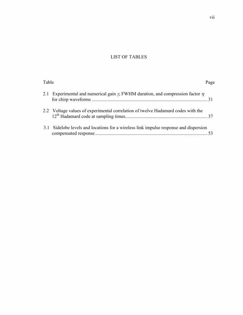
LIST OF TABLES
Table Page
2.1 Experimental and numerical gain , FWHM duration, and compression factor
for chirp waveforms ................................................................................................. 31
2.2 Voltage values of experimental correlation of twelve Hadamard codes with the
12th
Hadamard code at sampling times ..................................................................... 37
3.1 Sidelobe levels and locations for a wireless link impulse response and dispersion
compensated response .............................................................................................. 53
viii
LIST OF FIGURES
Figure Page
1.1 Photonic processing of analog RF signals ................................................................. 2
1.2 Matched filtering via correlation processing.............................................................. 4
1.3 Multitap microwave photonic filter (adapted from [30]) ........................................... 9
1.4 A multitap microwave photonic filter transfer function (adapted from [30]) .......... 10
1.5 Multitap microwave photonic filter based on multiple CW lasers (adapted from
[30]) ....................................................................................................................... 11
2.1 Photonic generation and compression of ultra-broadband RF waveforms .............. 14
2.2 VIPA structure ......................................................................................................... 15
2.3 VIPA as a spectral disperser (adapted from [63]) .................................................... 16
2.4 VIPA model (adapted from [63]) ............................................................................. 16
2.5 Output angle vs. wavelength for VIPA (adapted from [62]) ................................... 17
2.6 FT pulse shaper in transmissive geometry based on diffraction gratings ................ 17
2.7 Hyperfine FT pulse shaper in reflective geometry based on VIPA .......................... 18
2.8 Calibration setup for SLM in an optical pulse shaper .............................................. 19
2.9 Calibration raw data set ........................................................................................... 19
2.10 Pixel location vs. wavelength. Experimental results, linear and quadratic curve
fits are in solid circles, dashed and solid lines respectively. ................................. 20
2.11 RF photonic programmable matched filter ............................................................. 22
ix
Figure Page
2.12 RF photonic AWG .................................................................................................. 23
2.13 (a) Experimentally synthesized input linear chirp electrical waveform with >15
GHz frequency content centered at ~7.5 GHz. (b) Experimental output linear
chirp electrical waveform when the pulse shaper is quiescent. (c) Experimental
output compressed electrical waveform after the matched filter is applied. (d)
Calculated ideal photonically compressed electrical waveform ............................ 25
2.14 (a) Calculated spectral phases of the waveforms in Fig. 2.13 (b) and (c) are
shown in squares and solid circles respectively. (b) Calculated spectral
amplitudes of the waveforms in Fig. 2.13 (b) and (c) are shown in squares and
solid circles respectively ........................................................................................ 27
2.15 (a) Output linear chirp electrical waveform with ~12.5 GHz BW centered at
~6.25 GHz when the pulse shaper is quiescent. (b) Output compressed
electrical waveform after the matched filter is applied. (c) Calculated ideally
compressed electrical waveform ........................................................................... 28
2.16 (a) Output linear chirp electrical waveform with ~10 GHz BW centered at ~5
GHz when the pulse shaper is quiescent. (b) Output compressed electrical
waveform after the matched filter is applied. (c) Calculated ideally compressed
electrical waveform ............................................................................................... 29
2.17 (a) Output linear chirp electrical waveform with ~7.5 GHz BW centered at
~3.75 GHz when the pulse shaper is quiescent. (b) Output compressed
electrical waveform after the matched filter is applied. (c) Calculated ideally
compressed electrical waveform ........................................................................... 30
2.18 (a) Experimentally synthesized input 15-chip PR electrical waveform. (b)
Experimental output 15-chip PR electrical waveform when the pulse shaper is
quiescent. (c) Experimental output compressed electrical waveform after the
matched filter is applied. (d) Calculated ideal photonically compressed
electrical waveform ............................................................................................... 32
2.19 (a) Calculated spectral phases of the waveforms in Fig. 2.18 (b) and (c) are
shown in squares and solid circles respectively. (b) Calculated spectral
amplitudes of the waveforms in Fig. 2.18 (b) and (c) are shown in squares and
solid circles respectively ........................................................................................ 33

x
Figure Page
2.20 (a) Output periodic 15-chip PR sequence waveform at 13.5 Gb/s when the pulse
shaper is quiescent. (b) Output compressed electrical waveform after the
matched filter is applied. (c) Calculated ideally compressed electrical
waveform ............................................................................................................... 34
2.21 (a) Output 12th
Hadamard code waveform at 13.5 Gb/s when the pulse shaper is
quiescent. (b) Output compressed electrical waveform after the matched filter
is applied. (c) Calculated ideally compressed electrical waveform ....................... 36
2.22 Output Hadamard code waveforms from 1st to 12
th codes at 13.5 Gb/s as solid
line when the pulse shaper is quiescent. Output Hadamard code waveforms
correlated with the 12th
Hadamard code waveform in grey line ............................ 37
2.23 Operation of a matched filter in presence of additive white Gaussian noise .......... 38
2.24 Simplified RF photonic matched filter block diagram............................................ 39
2.25 Gain parameter vs. frequency bandwidth for ultra-broadband RF chirp electrical
waveforms. The circles show the experimental gain parameter vs. the
frequency corresponding to the chirp fastest oscillation cycle. The squares
show the calculated gain parameter after processing waveforms through an
ideal photonically matched filter. The dashed line shows the maximum
theoretical gain parameter given by (2.29) ............................................................ 44
3.1 The LOS antenna link configuration ........................................................................ 46
3.2 (a) Measured time domain response of a ridged TEM horn antenna link. The 30-
ps driving pulse is shown in the inset. (b) The antenna link frequency response,
relative amplitude and phase extracted from the time domain response ............... 47
3.3 Experimental setup for post-compensation of dispersion. The LOS antenna link
is followed by an RF amplifier and the RF photonic phase filter .......................... 48
3.4 (a) Output electrical waveform when the pulse shaper is quiescent. (b) Output
dispersion compensated electrical waveform after the phase filter is applied,
and calculated dispersion-compensated electrical waveform by an ideal
photonic phase filter as solid and dashed lines respectively ................................. 50
3.5 Comparison of normalized power for: (a) The antenna link impulse response. (b)
Measured dispersion-compensated waveform. (c) Calculated dispersion-
compensated waveform ......................................................................................... 52
xi
Figure Page
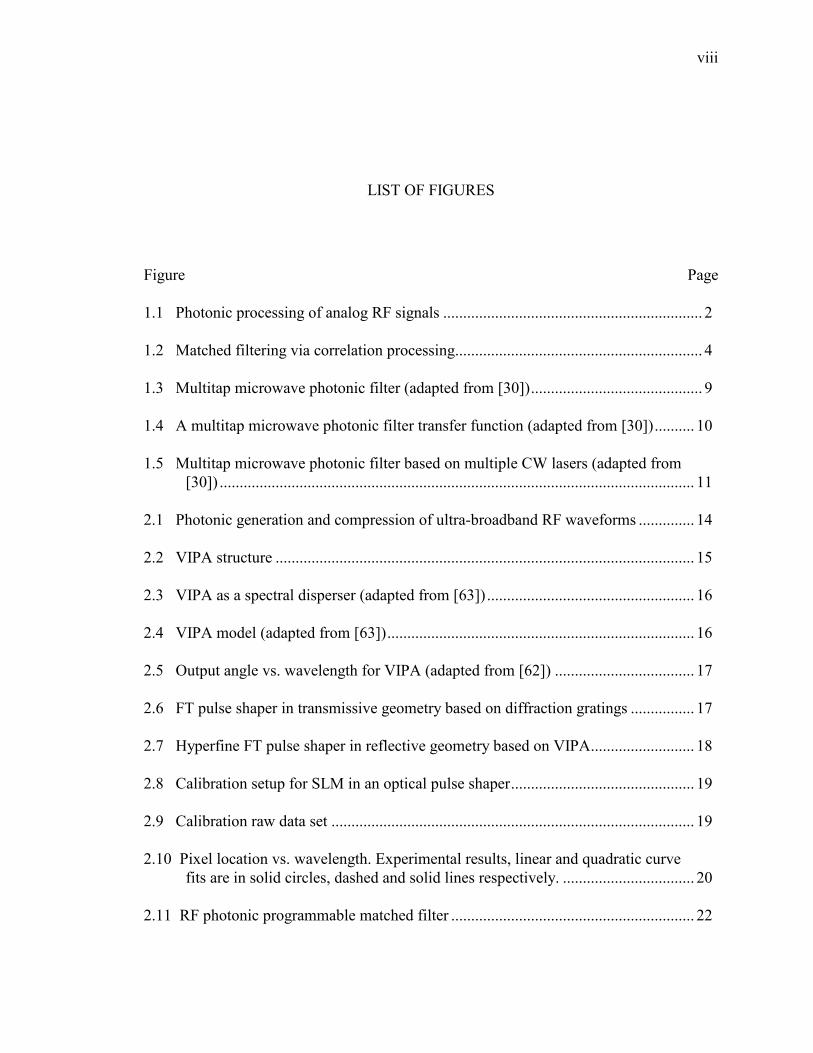
3.6 Radar configuration.................................................................................................. 53
3.7 (a) Radar link response with TM reflection without the phase filter. (b) Radar
link response after applying the dispersion compensating filter. Magnified view
of two highly resolved pulses shown in the inset. ................................................. 55
3.8 (a) Radar link response with TE reflection without the phase filter. (b) Radar link
response after applying the dispersion compensating filter ................................... 56
3.9 Experimental setup for waveform identification. 15-chip PR sequence is
generated by Agilent N4901 Serial Bit Error Rate Tester and transmitted via
the wireless link followed by an RF amplifier and the RF photonic phase filter .. 58
3.10 (a) Generated 15-chip PR sequence waveform. (b) Experimental and simulated
distorted PR sequence received through the antenna link in solid and dashed
lines respectively. (c) Output of the RF photonic filter when the pulse shaper is
quiescent. (d) Experimental and simulated retrieved PR sequence after
compensating the antenna link dispersion in solid and dashed lines
respectively. (e) Experimental and simulated received waveform after
compensating the antenna link dispersion and conjugate phase filtering the PR
sequence waveform in solid and dashed lines respectively ................................... 59
4.1 Configuration of programmable microwave photonic filter .................................... 62
4.2 The microwave photonic link frequency response without DCF. ............................ 66
4.3 (a) Unapodized optical comb. (b) Normalized and simulated filter transfer
functions in solid and dashed lines respectively. The vertical dashed lines
depict individual Nyquist zones, where m refers to the zone number, explained
in the text. The filter can be used in a spur free regime within the span of any
one of these zones. ................................................................................................. 68
4.4 (a) Gaussian apodized optical comb. (b) Normalized and simulated filter transfer
functions in solid and dashed lines respectively. ................................................... 69
4.5 (a) Normalized and simulated filter transfer functions for unapodized comb in
solid and dashed lines respectively. (b) Normalized and simulated filter transfer
functions for apodized comb in solid and dashed lines respectively. .................... 70
4.6 Simulated filter transfer function for an ideally Gaussian apodized comb .............. 71
xii
Figure Page
4.7 (a) Optical frequency comb. (b) Normalized and simulated filter transfer
functions for compensated comb in solid and dashed lines respectively. (c)
Normalized and simulated filter transfer functions for uncompensated comb in
solid and dashed lines respectively ........................................................................ 73
4.8 Configuration of tunable programmable microwave photonic filter ....................... 75
4.9 (a) Gaussian apodized optical frequency comb. (b) Normalized and simulated
filter transfer functions for m.100-20 ps relative delay in solid and dashed lines
respectively. (c) Normalized and simulated filter transfer functions for m.100-
50 ps relative delay in solid and dashed lines respectively ................................... 79
4.10 Tunable filter passband center vs. relative delay .................................................. 80
4.11 Configuration of multitap microwave photonic filter with complex coefficient
taps ......................................................................................................................... 81
4.12 (a) Unapodized optical frequency comb. (b) Normalized and simulated filter
transfer function in solid and dashed lines respectively ........................................ 82
4.13 The normalized measured filter transfer functions for a linearly increasing phase
in steps of -/8, /8, /4 and /2 in (a), (b), (c) and (d) respectively .................... 83
4.14 Configuration of microwave photonic filter based on IM biased at minimum
transmission ........................................................................................................... 86
4.15 (a) Unapodized optical frequency comb. (b) Measured and simulated filter
transfer functions in solid and dashed lines respectively ...................................... 87
4.16 (a) Gaussian apodized optical frequency comb. (b) (c) (d) Measured and
simulated filter transfer functions for relative delays of m.100+29 ps, m.100+10
ps and m.100+48 ps respectively ........................................................................... 88
Appendix Figure
B.1 Transfer functions when RF power applied to the first arm 3-dB stronger and
weaker than RF power applied to the second arm in solid and dashed lines
respectively .......................................................................................................... 109
B.2 Transfer functions when optical power in the second arm is 3-dB weaker and
stronger in solid and dashed lines respectively ................................................... 110

xiii
Figure Page
B.3 Transfer functions when the RF signals have 100 and 80 degrees phase
difference in solid and dashed lines respectively ................................................ 111
B.4 Maximum transfer function variation vs. RF power imbalance applied to the
arms of dual-drive modulator .............................................................................. 111
B.5 Maximum transfer function variation vs. phase difference between RF signals
applied to the arms of dual-drive modulator ....................................................... 112
B.6 Amplitude frequency responses of hybrid’s 0 and 90-degree ports in black and
grey respectively .................................................................................................. 112
B.7 Phase frequency responses of hybrid’s 0 and 90-degree ports in black and grey
respectively .......................................................................................................... 113
B.8 Measured transfer function of the RF photonic link with 60-km SMF ................. 113
B.9 Simulated transfer function of the RF photonic link with 60-km SMF using the
measured hybrid scattering parameters ............................................................... 114
C.1 Model for microwave photonic filter based on IM ............................................... 115
C.2 Model for microwave photonic filter based on a dual-drive modulator ................ 116
C.3 Model for tunable microwave photonic filter based on SSB modulation and
interferometric scheme ........................................................................................ 118
C.4 Model for tunable microwave photonic filter based on IM and interferometor .... 119
D.1 (a) Flat comb. (b) Gaussian apodized comb. (c) Simulated filter transfer
functions for flat and Gaussian tap profiles in grey and black lines respectively 122
D.2 SLS and 3-dB BW as a function of maxline-to-minline extinction of a Gaussian
apodized comb with 100 lines ............................................................................. 123
D.3 SLS for >1.5FWHM away from the bandpass center and 3-dB BW as a function
of comb maxline-to-minline extinction ............................................................... 123
D.4 The filter transfer function for Gaussian apodized comb with maxline-to-minline
extinction of 10.5 dB and 32 lines ....................................................................... 124

xiv
Figure Page
D.5 SLS for >750 MHz away from the bandpass center and the corresponding 3-dB
BW as a function of minimum required number of lines .................................... 124
xv
LIST OF ABBREVIATIONS
ASE Amplified spontaneous emission
AWG Arbitrary waveform generator
BW Bandwidth
CDMA Code division multiple access
CW Continuous wave
DCF Dispersion compensating fiber
DPSK Differential phase shift keying
DSB Double-sideband
EDFA Erbium doped fiber amplifier
FCC Federal communications commission
FIR Finite impulse response
FFT Fast Fourier transform
FSR Free spectral range
FT Fourier transform
FWHM Full width at half maximum
IF Intermediate frequency
LCM Liquid crystal modulator
LOS Line of sight
MEMS Micro-electro-mechanical systems
MZ Mach-Zehnder
O/E Optical-to-electrical
OSA Optical spectrum analyzer
PD Photodetector, or Photodiode
PR Pseudorandom
RF Radio frequency
SAW Surface acoustic wave
SLM Spatial light modulator
SLS Sidelobe suppression
SMF Single mode fiber
SNR Signal-to-noise ratio
SSB Single-sideband
TE Transverse electric
TEM Transverse electromagnetic
TM Transverse magnetic

xvi
UWB Ultra-wideband
VIPA Virtually imaged phased array
VNA Vector network analyzer

xvii
ABSTRACT
Hamidi, Ehsan. Ph.D., Purdue University, December 2010. Photonic Processing of Ultra-
broadband Radio Frequency Waveforms. Major Professor: Andrew M. Weiner.
Photonic processing has been significantly explored in the past few decades to
process electrical signals; however, photonic processing of ultra-broadband signals with
bandwidths in excess of multi GHz and large fractional bandwidth has been less
investigated with minimal attention given to time domain aspects. Moreover photonic
processing benefits from properties such as large bandwidth, immunity to electromagnetic
interference, tunability, and programmability compared to electrical processing. Therefore
radio frequency photonic techniques can be utilized to enhance the performance of analog
radio frequency systems in detection and filtering of ultra-broadband signals.
We present the first implementation of radio frequency photonic matched filter
based on hyperfine optical pulse shaping to compress ultra-broadband arbitrary radio
frequency waveforms to their bandwidth limited duration. This filter which has a
programmable arbitrary frequency response enables real-time fast processing of ultra-
broadband signals. Further more the application of this technique to post-compensate
broadband antenna’s dispersion will be demonstrated which potentially pushes ultra-
broadband radio frequency systems and radars toward dispersion free performance.
Finally for the first time tunable programmable microwave photonic filters based on
optical frequency combs are implemented. These filters have finite impulse response with
tap weights programmed by arbitrary complex coefficients. The large number of comb
lines provides more freedom to shape the bandpass filter while tunability is achieved
using an interferometric scheme.
1
1. INTRODUCTION
Photonic processing of electrical signals has been investigated for the past three
decades [1] to enhance the performance of radio frequency (RF) systems, and is
categorized under RF photonics which is also alternately referred as microwave photonics
[2]. In early years, RF photonics focused on delay lines with application in phased array
antennas [3], and developed into versatile techniques as RF photonic filters [4-13], and
finally RF photonic waveform generators were introduced [14-22]. RF photonics offers
lot of advantages such as ultra-broad bandwidth, immunity to electromagnetic
interference, flexibility, low loss, etc. [2].
During the past decade many photonic techniques have been developed for
generation of arbitrary RF waveforms with instantaneous bandwidths exceeding the multi
GHz values available via electronic arbitrary waveform generator (AWG) technology. A
prominent technique is based on optical spectrum shaping followed by frequency to time
mapping in a dispersive medium and then optical-to-electrical (O/E) conversion for the
generation of arbitrary RF electrical waveforms which has demonstrated tens of GHz of
bandwidth [16, 19]. Later on these photonically generated RF waveforms were used to
compensate broadband antenna dispersion [23, 24] and to measure antennas’ frequency
dependent delay [25]. Although a lot of effort has been devoted to the generation of RF
waveforms via photonic techniques, still practical ways to process and detect ultra-
broadband electrical signals for applications in RF systems are lacking [26]. On the other
hand, digital ultra-wideband (UWB) receivers which are based on sampling and digital
signal processing are limited by the analog-to-digital (A/D) converters’ speed and
dynamic range [27]. Also the state-of-the-art in implementing a UWB receiver is limited
to bandwidths much less than the UWB frequency band [28]. Hence, photonic processing
2
of RF waveforms is an interesting candidate for processing ultra-broadband electrical
signals in wireless systems [29].
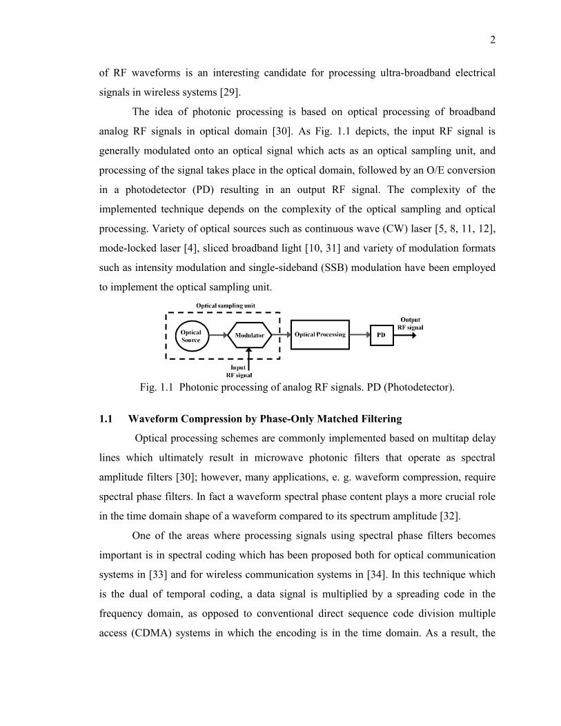
The idea of photonic processing is based on optical processing of broadband
analog RF signals in optical domain [30]. As Fig. 1.1 depicts, the input RF signal is
generally modulated onto an optical signal which acts as an optical sampling unit, and
processing of the signal takes place in the optical domain, followed by an O/E conversion
in a photodetector (PD) resulting in an output RF signal. The complexity of the
implemented technique depends on the complexity of the optical sampling and optical
processing. Variety of optical sources such as continuous wave (CW) laser [5, 8, 11, 12],
mode-locked laser [4], sliced broadband light [10, 31] and variety of modulation formats
such as intensity modulation and single-sideband (SSB) modulation have been employed
to implement the optical sampling unit.
Fig. 1.1 Photonic processing of analog RF signals. PD (Photodetector).
1.1 Waveform Compression by Phase-Only Matched Filtering
Optical processing schemes are commonly implemented based on multitap delay
lines which ultimately result in microwave photonic filters that operate as spectral
amplitude filters [30]; however, many applications, e. g. waveform compression, require
spectral phase filters. In fact a waveform spectral phase content plays a more crucial role
in the time domain shape of a waveform compared to its spectrum amplitude [32].
One of the areas where processing signals using spectral phase filters becomes
important is in spectral coding which has been proposed both for optical communication
systems in [33] and for wireless communication systems in [34]. In this technique which
is the dual of temporal coding, a data signal is multiplied by a spreading code in the
frequency domain, as opposed to conventional direct sequence code division multiple
access (CDMA) systems in which the encoding is in the time domain. As a result, the

3
signal will be spread in time due to arbitrary spectral phase. At the receiver, the received
signal spectrum is multiplied by the conjugate of the spreading signal spectrum to retrieve
the data or in other words to decode the signal. Hence this technique requires Fourier
transform (FT) of signals for processing waveforms since multiplication takes place in the
frequency domain.
In optical communication systems, spectral coding has been easily realized
through FT optical pulse shaping which acts as an optical spectral phase filter [35].
Although in wireless communication systems, accessing Fourier transform of signals is
not easy to achieve and therefore spectral coding and decoding are performed by using
surface acoustic wave (SAW) devices. Due to difficulties and challenges in fabricating
SAW correlators, they have been demonstrated only for center frequencies up to 3.63
GHz with 1.1-GHz bandwidth (BW) which is only 30% fractional bandwidth with
insertion loss of 23 dB even after accounting for the compression gain [36]. This
frequency bandwidth is well below the UWB frequency band (3.1-10.6 GHz) allocated by
the Federal Communications Commission (FCC) [37] and bandwidths accessible via RF
photonic AWG techniques with almost 200% fractional bandwidth.
Matched filters are commonly used in communication systems for maximizing the
signal-to-noise ratio (SNR) of the received signal in presence of additive white Gaussian
noise [38, 39]. By definition a matched filter is a linear time-invariant filter such that its
impulse response is a time-reversed version of the specified signal. As we will discuss in
details later this definition leads to a filter such that its spectral phase response is a
conjugate of the signal spectral phase. The operation of this filter on the corresponding
signal without noise results in an output signal which has a linear spectral phase due to
multiplication in frequency domain. In other words the output waveform will be
compressed to its bandwidth limited duration. This property of a matched filter can be
used as a spectral decoding technique in communication systems. The phase only
matched filters have been already investigated in optics area [40].
Conventionally a matched filter is implemented via correlation [39] as illustrated
in Fig. 1.2 in which a received signal, r(t) is multiplied with the specified signal, s(t) and
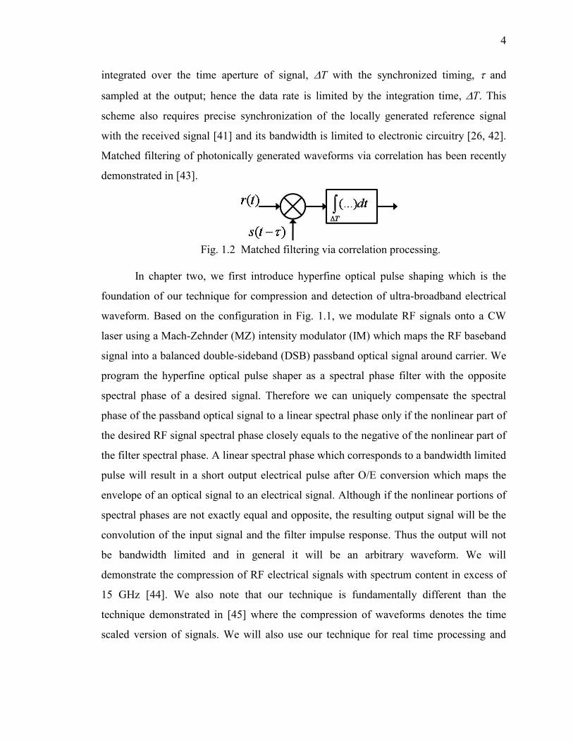
4
integrated over the time aperture of signal, T with the synchronized timing, and
sampled at the output; hence the data rate is limited by the integration time, T. This
scheme also requires precise synchronization of the locally generated reference signal
with the received signal [41] and its bandwidth is limited to electronic circuitry [26, 42].
Matched filtering of photonically generated waveforms via correlation has been recently
demonstrated in [43].
Fig. 1.2 Matched filtering via correlation processing.
In chapter two, we first introduce hyperfine optical pulse shaping which is the
foundation of our technique for compression and detection of ultra-broadband electrical
waveform. Based on the configuration in Fig. 1.1, we modulate RF signals onto a CW
laser using a Mach-Zehnder (MZ) intensity modulator (IM) which maps the RF baseband
signal into a balanced double-sideband (DSB) passband optical signal around carrier. We
program the hyperfine optical pulse shaper as a spectral phase filter with the opposite
spectral phase of a desired signal. Therefore we can uniquely compensate the spectral
phase of the passband optical signal to a linear spectral phase only if the nonlinear part of
the desired RF signal spectral phase closely equals to the negative of the nonlinear part of
the filter spectral phase. A linear spectral phase which corresponds to a bandwidth limited
pulse will result in a short output electrical pulse after O/E conversion which maps the
envelope of an optical signal to an electrical signal. Although if the nonlinear portions of
spectral phases are not exactly equal and opposite, the resulting output signal will be the
convolution of the input signal and the filter impulse response. Thus the output will not
be bandwidth limited and in general it will be an arbitrary waveform. We will
demonstrate the compression of RF electrical signals with spectrum content in excess of
15 GHz [44]. We also note that our technique is fundamentally different than the
technique demonstrated in [45] where the compression of waveforms denotes the time
scaled version of signals. We will also use our technique for real time processing and
5
correlation of pseudorandom (PR) sequences and orthogonal sequences such as
Hadamard codes.
1.2 Dispersion Compensation of Broadband Antennas
Interest in UWB systems has grown rapidly due to appealing features such as high
data rate, multi-access and low probability of intercept communications. The application
of UWB to ranging and radar has also received attention [46, 47], due to its potential for
hyperfine range resolution. Although the efficient use of single carrier, large fractional
bandwidth signals that efficiently utilize the ultrawide bandwidth allocated by FCC [37]
remains a challenge. Manipulation of large instantaneous bandwidth UWB signals incurs
challenges related to generation, transmission and detection.
One of the key limitations in UWB transmission system [42], particularly in line
of sight (LOS), is signal distortion due to dispersion and frequency dependent
transmission. Channel non-uniformity assuming no emission regulation is arising from
non-uniform spectral amplitude response of the channel including the receiver and
transmitter elements which determines the effective channel bandwidth. To overcome this
limitation shaping the transmitting signal spectrum has been proposed in [48]. Shaping of
the power spectrum has been demonstrated by utilizing RF photonic AWG to tailor the
spectral amplitude of transmitting signals according to UWB emission regulation [49].
Dispersion due to the nonlinear RF spectral phase response of the transmitter
and/or receiver elements is the focus of our investigation. In particular, for large
fractional bandwidth signals, some of antennas utilized in a wireless link may contribute
very large dispersion to the signal due their physical structure and frequency dependent
impedance [50, 51]. This problem has been theoretically investigated, and optimization of
transmit waveforms in order to optimize the received signal amplitude, energy, or
duration has been analyzed [52]. Recently experiments have been reported in which
photonically generated UWB RF waveforms were synthesized in order to successfully
precompensate for antenna dispersion [23, 24]. The application of photonically generated
6
arbitrary waveforms to measure the frequency dependent delay of broadband antennas has
also been demonstrated [25].
In principle the precompensation technique relies on the generation of a transmit
signal shaped according to the time-reversed impulse response of the link. Although in
point-to-multipoint systems when diversity is present among receivers, e.g. different
receive antennas, this technique can not compensate all the links simultaneously.
Furthermore, in the context of wireless communications, when the delay between
adjacent symbols is less than the time spread of the impulse response, this technique
requires synthesis of a waveform equal to the coherent combination of two or more
delayed precompensation waveforms. This adds to the complexity required from the
AWG and may exceed current capabilities.
Alternately, real-time post-processing to remove dispersion can be performed at
the front end of the receiver. This resolves the problems of receiver diversity and AWG
complexity. Here, by connecting the output of a receiving antenna to a programmable
UWB phase filter implemented in photonics, we demonstrate compensation of the
dispersion associated with antennas in a LOS wireless link. In addition, we also
demonstrate waveform identification functionality through appropriate programming of
the phase filter.
The FCC’s regulation on UWB emission includes a constraint on full bandwidth
peak power, which has been analyzed as a function of repetition rate for various pulse
bandwidths [53]. It is shown that for repetition rates less than 187.5 kHz, the full
bandwidth peak power constraint dominates the average power spectral density
constraint. Therefore, for a fixed bandwidth one may transmit higher energy at the
allowed peak power by utilizing waveforms that are spread in time by the application of
spectral phase modulation.
On the other hand in radar systems where high energy pulses are required at low
repetition rates, the amplification of large fractional bandwidth pulses becomes a bottle-
neck because of the trade-off between bandwidth and output swing in RF power
amplifiers. In order to increase the pulse energy at a fixed peak voltage, bandwidth
7
limited pulses are commonly replaced by spread-time waveforms which are spectrally
phase modulated, e.g. linear chirp [54]. Conventionally the return signal is correlated
with a replica of the transmit signal to obtain compression and realize the ultimate range
resolution. Although this scheme requires accurate timing between received waveforms
and reference signals and must be performed in multiple shots or in multi-channel
processors [54] in absence of prior knowledge of return signal delay. These problems are
particularly difficult when the bandwidths are very large. A different solution is to use a
real-time spectral phase filter, which cancels the spectral phase of the waveform. This
compresses the waveform to the bandwidth limit, which can be used to improve SNR
and better resolve closely spaced return signals. In this context we further demonstrate
compression of arbitrary waveforms by simultaneously phase compensating the
waveform itself and dispersion compensating the wireless link [55].
In chapter three, we utilize the technique introduced in chapter two for the
dispersion compensation of wireless links caused by the nonlinear spectral phase of
broadband antennas. We demonstrate how we compress a chirp impulse response of a
pair of ridged TEM (Transverse Electromagnetic) horn antennas in LOS to its bandwidth
limited duration after the receiving antenna. Therefore we are able to overcome the
antenna’s introduced distortion. This technique improves the time domain resolution
which can increase the range resolution of ultra-broadband radars while combined with
the matched filtering scheme it enables real-time processing of received signals in radars
[55].
1.3 Tunable Programmable Microwave Photonic Filters
Microwave filter design area has been conventionally the focus of implementation
of electrical filters for different applications in communication systems. Although there
have been significant advances in this area, still there are desired filter properties that can
not be achieved simultaneously. The trade-off among different filter aspects sets
constraints on the state-of-the-art filters. Filter sharpness, selectivity, loss, tunability,
8
programmability and noise figure are some of the most important filter parameters [56].
Here we briefly review the current technology in microwave filter design.
High selectivity and sharpness require high order filter which results in high loss.
These high order filters are usually not programmable or tunable; however, they can be
slightly altered after fabrication, for example by introducing a metal rod into a filter
resonator the center frequency of the bandpass filter can be adjusted. As an example, an
eight-pole filter based on microstrip technology has been demonstrated in [57].
In order to overcome high loss, the application of high temperature
superconductors has led into extremely low loss, highly selective and sharp filters. A
filter with twenty poles has been reported in [58]. As we notice achieving high selectivity
with low loss requires high quality factor components which prevents us from fabricating
tunable filters.
The implementation of tunable filters in microwave engineering mainly relies on
Micro-Electro-Mechanical Systems (MEMS) technology. Although these filters can
achieve a large tunable range with a reasonable loss, their orders usually do not exceed
few poles and as a result the filter passband can not be configured to a great extent [59,
60].
In summary implementation of programmable tunable filters with high selectivity
and sharpness and low loss remains a challenge in microwave filter design. High
selectivity and sharpness require high order filters which results in high loss. To obtain
low loss filters, utilization of high quality factor components becomes essential; however,
tunable components generally have low quality factors. Therefore there has been growing
interest in microwave photonic filters in the past few decades due to their
programmability and tunability over a large bandwidth. The dominant schemes in
microwave photonic filters are based on multitap filters which are discussed in following.
The multitap delay line concept is the basis of two most common categories of
microwave photonic filters [30]. In the first scheme which is shown in Fig. 1.3, the RF
signal is modulated onto an optical source and then demultiplexed into a number of
physical optical delay lines. The outputs are multiplexed together and fed into a PD to

9
convert the optical signal to an electrical signal. In order to have a configuration free from
environmental effects and thus stable and repeatable performance, the source coherence
time is chosen much smaller than the differential delay between taps, resulting in an
incoherent regime in which the photodetector output is the sum of the optical powers of
the filter samples. Although the shape of the filter transfer function can be programmed
by adjusting the tap weights, generally the peak of the bandpass is set by the differential
delay between taps and may not be tuned. The resulting filter impulse response is given
by
N
kk kTtath
0
)()( (1.1)
where T is the differential delay between taps and ak’s are the tap coefficients. Here we
note that since a tap weight is proportional to power intensity it can only take a definite
positive value. Hence only filters with impulse responses which sample by positive
coefficients can be implemented through this scheme. By Fourier transformation of the
impulse response we obtain the frequency response of the filter as
N
k
TjkkeaH
0
)( (1.2)
Fig. 1.3 Multitap microwave photonic filter (adapted from [30]).

10
The above expression represents a transfer function with a periodic spectral
characteristic as shown in Fig. 1.4. The filter free spectral range (FSR) is inversely
proportional to the tap delay spacing T and the bandpass full width at half maximum
(FWHM) is given by
Q
FSRFWHM (1.3)
where Q is the quality factor which relates to the number of taps and for uniformly
weighted taps is approximately equals to the number of taps N. We note that the bandpass
center can be tuned by controlling the delay T. As we notice, the filter bandpass
characteristic may be controlled by adjusting the taps’ weights.
A multitap microwave photonic filter can be also implemented based on the
configuration shown in Fig. 1.5 which has been explored more recently. In this scheme
the delay lines are replaced by an optical source comprising multiple optical frequencies
and a dispersive medium. Each optical carrier experiences a wavelength dependent delay
due to the medium dispersion. By equally spacing of the carriers in frequency, taps with
equal delay spacing will be obtained. The weight of each tap can be adjusted by
controlling the intensity of corresponding carrier. We may characterize the performance
of the filter similar to the foregoing analysis, and we can show the impulse response of
the filter is given by (1.1) where ak’s are the intensity of optical carriers.
Fig. 1.4 A multitap microwave photonic filter transfer function (adapted from [30]).
The multiple frequency source has been implemented by using a mode-locked
laser, by combining a few CW sources, or a spectrally sliced broadband source. Due to
cost, it is difficult to reach a large number of taps by combining many CW lasers. Slicing
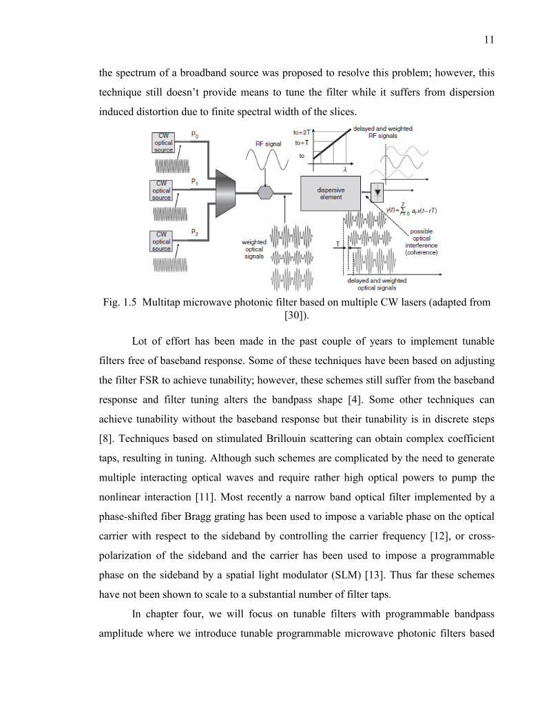
11
the spectrum of a broadband source was proposed to resolve this problem; however, this
technique still doesn’t provide means to tune the filter while it suffers from dispersion
induced distortion due to finite spectral width of the slices.
Fig. 1.5 Multitap microwave photonic filter based on multiple CW lasers (adapted from
[30]).
Lot of effort has been made in the past couple of years to implement tunable
filters free of baseband response. Some of these techniques have been based on adjusting
the filter FSR to achieve tunability; however, these schemes still suffer from the baseband
response and filter tuning alters the bandpass shape [4]. Some other techniques can
achieve tunability without the baseband response but their tunability is in discrete steps
[8]. Techniques based on stimulated Brillouin scattering can obtain complex coefficient
taps, resulting in tuning. Although such schemes are complicated by the need to generate
multiple interacting optical waves and require rather high optical powers to pump the
nonlinear interaction [11]. Most recently a narrow band optical filter implemented by a
phase-shifted fiber Bragg grating has been used to impose a variable phase on the optical
carrier with respect to the sideband by controlling the carrier frequency [12], or cross-
polarization of the sideband and the carrier has been used to impose a programmable
phase on the sideband by a spatial light modulator (SLM) [13]. Thus far these schemes
have not been shown to scale to a substantial number of filter taps.
In chapter four, we will focus on tunable filters with programmable bandpass
amplitude where we introduce tunable programmable microwave photonic filters based
12
on optical frequency combs. As depicted in Fig. 1.1 we employ optical frequency comb
combined with a Lithium Niobate MZ modulator which acts as an optical sampling unit.
A dispersive medium such as single mode fiber (SMF) before the photodiode (PD)
imposes a wavelength dependent delay on the comb lines which serve as filter taps. The
application of optical frequency combs benefits from large number of lines that can be
scaled to a larger number of lines without significant additional complexity resulting in
multitap microwave photonic filters with large number of taps. We will introduce line-by-
line optical pulse shaping as a tool for controlling the intensity of individual comb lines
which enables shaping the bandpass of resulting microwave photonic filters. The line-by-
line optical pulse shaping is based on high resolution Fourier transform optical pulse
shaper using diffraction gratings. To achieve filter tunability we will employ a novel
interferometric scheme which introduces a linearly incremental programmable phase
across taps by controlling an optical delay resulting in a tunable filter [61].
1.4 Concluding Additions
In chapter five, we will provide a summary of techniques which we have
developed and demonstrated. We will describe their importance and possibilities where
they can be utilized to improve the technology. We will briefly point out future research
opportunities in the field of photonic processing of RF signals and we will also explain
the possibility of using other technologies in the aforementioned techniques to improve
their performance, to integrate and to optimize important parameters such as loss, size,
nonlinearity, bandwidth, stability, etc.
There are four appendices which are devoted for further details and discussions
which didn’t seem necessary in the body of chapters. Appendix A deals with the
theoretical derivation of matched filtering parameters for periodic chirp waveforms with
100% duty cycle. Appendix B investigates the effect of unbalanced DSB modulation on
the performance of microwave photonic filters introduced in chapter four through
derivation, experiment and simulation. Appendix C provides a complete derivation of
microwave photonic filters’ RF gain in different configurations introduced in chapter

13
four. Appendix D discusses the filter parameters such as sidelobe suppression (SLS) and
3-dB bandwidth for a Gaussian profile comb with respect to the number of comb lines
and apodization through simulation.
14
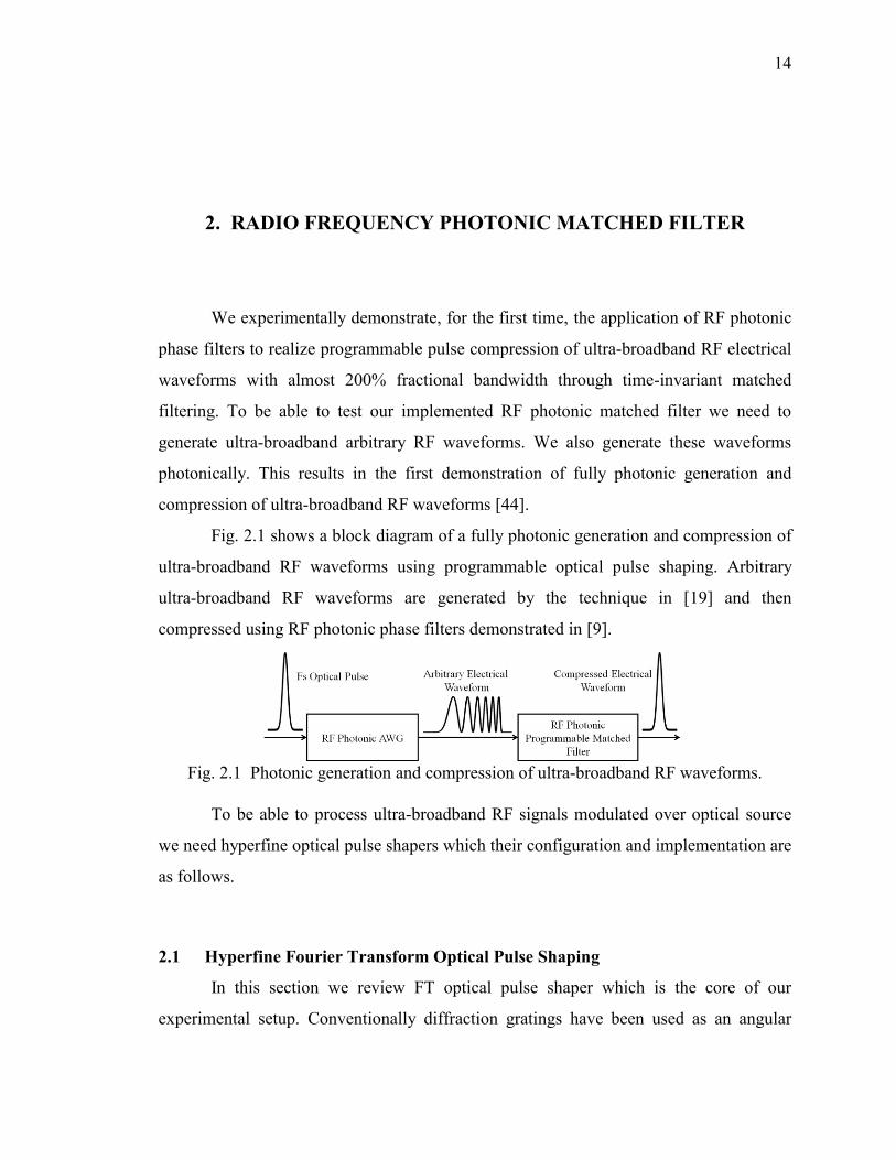
2. RADIO FREQUENCY PHOTONIC MATCHED FILTER
We experimentally demonstrate, for the first time, the application of RF photonic
phase filters to realize programmable pulse compression of ultra-broadband RF electrical
waveforms with almost 200% fractional bandwidth through time-invariant matched
filtering. To be able to test our implemented RF photonic matched filter we need to
generate ultra-broadband arbitrary RF waveforms. We also generate these waveforms
photonically. This results in the first demonstration of fully photonic generation and
compression of ultra-broadband RF waveforms [44].
Fig. 2.1 shows a block diagram of a fully photonic generation and compression of
ultra-broadband RF waveforms using programmable optical pulse shaping. Arbitrary
ultra-broadband RF waveforms are generated by the technique in [19] and then
compressed using RF photonic phase filters demonstrated in [9].
Fig. 2.1 Photonic generation and compression of ultra-broadband RF waveforms.
To be able to process ultra-broadband RF signals modulated over optical source
we need hyperfine optical pulse shapers which their configuration and implementation are
as follows.
2.1 Hyperfine Fourier Transform Optical Pulse Shaping
In this section we review FT optical pulse shaper which is the core of our
experimental setup. Conventionally diffraction gratings have been used as an angular
15
disperser in optical pulse shapers; however, an optical pulse shaper spectral resolution is
limited by the low angular dispersion of diffraction gratings. In following we will
introduce a highly dispersive device named Virtually Imaged Phased Array (VIPA) [62]
which we use to implement a hyperfine optical pulse shaper.
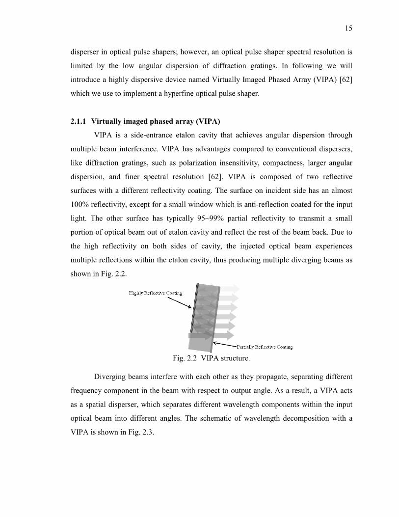
2.1.1 Virtually imaged phased array (VIPA)
VIPA is a side-entrance etalon cavity that achieves angular dispersion through
multiple beam interference. VIPA has advantages compared to conventional dispersers,
like diffraction gratings, such as polarization insensitivity, compactness, larger angular
dispersion, and finer spectral resolution [62]. VIPA is composed of two reflective
surfaces with a different reflectivity coating. The surface on incident side has an almost
100% reflectivity, except for a small window which is anti-reflection coated for the input
light. The other surface has typically 95~99% partial reflectivity to transmit a small
portion of optical beam out of etalon cavity and reflect the rest of the beam back. Due to
the high reflectivity on both sides of cavity, the injected optical beam experiences
multiple reflections within the etalon cavity, thus producing multiple diverging beams as
shown in Fig. 2.2.
Fig. 2.2 VIPA structure.
Diverging beams interfere with each other as they propagate, separating different
frequency component in the beam with respect to output angle. As a result, a VIPA acts
as a spatial disperser, which separates different wavelength components within the input
optical beam into different angles. The schematic of wavelength decomposition with a
VIPA is shown in Fig. 2.3.
16
Fig. 2.3 VIPA as a spectral disperser (adapted from [63]).
VIPA is named after the fact that the multiple partially reflected beams from
VIPA can be modeled as an array of individual images of the incident beam waist as
shown in Fig. 2.4. The spatial distance between virtual array elements results in constant
relative phase.
Fig. 2.4 VIPA model (adapted from [63]).
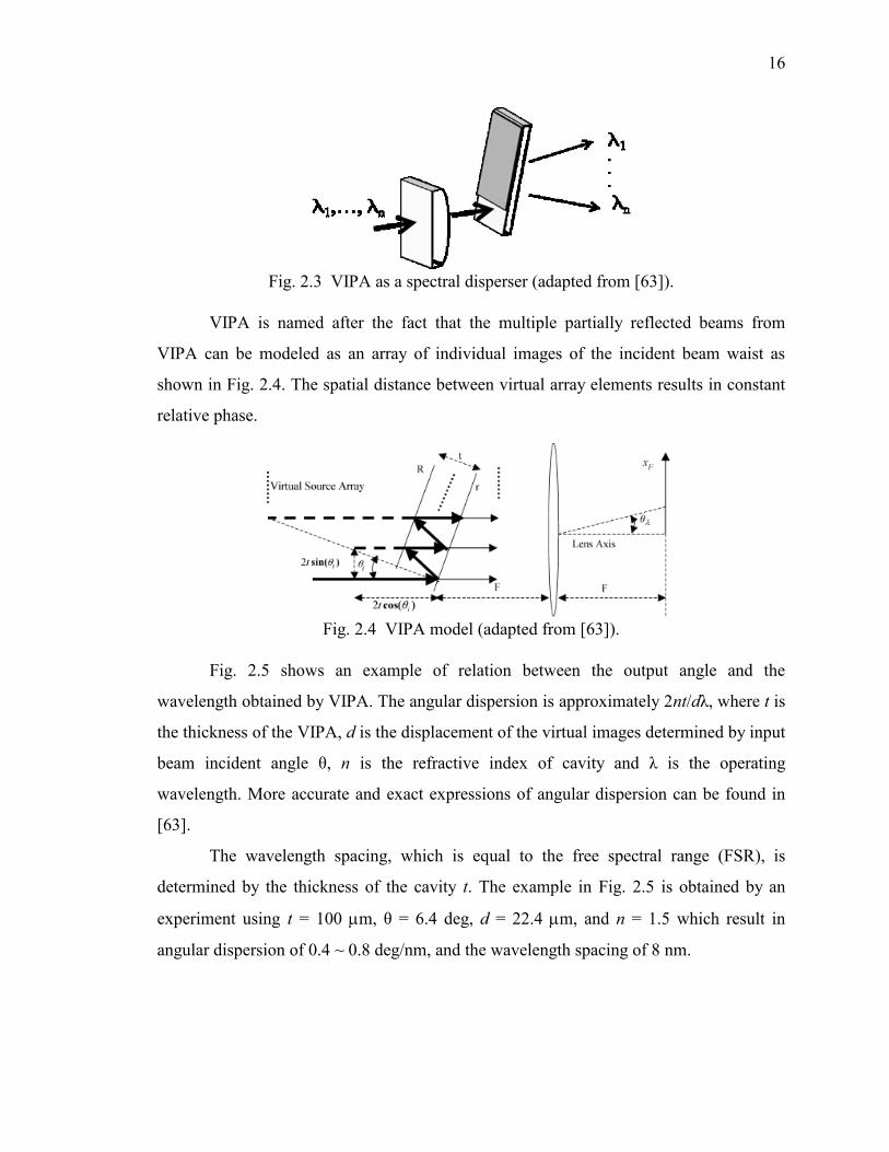
Fig. 2.5 shows an example of relation between the output angle and the
wavelength obtained by VIPA. The angular dispersion is approximately 2nt/dλ, where t is
the thickness of the VIPA, d is the displacement of the virtual images determined by input
beam incident angle θ, n is the refractive index of cavity and λ is the operating
wavelength. More accurate and exact expressions of angular dispersion can be found in
[63].
The wavelength spacing, which is equal to the free spectral range (FSR), is
determined by the thickness of the cavity t. The example in Fig. 2.5 is obtained by an
experiment using t = 100 m, θ = 6.4 deg, d = 22.4 m, and n = 1.5 which result in
angular dispersion of 0.4 ~ 0.8 deg/nm, and the wavelength spacing of 8 nm.
17
Fig. 2.5 Output angle vs. wavelength for VIPA (adapted from [62]).
2.1.2 Transmissive and reflective FT pulse shapers
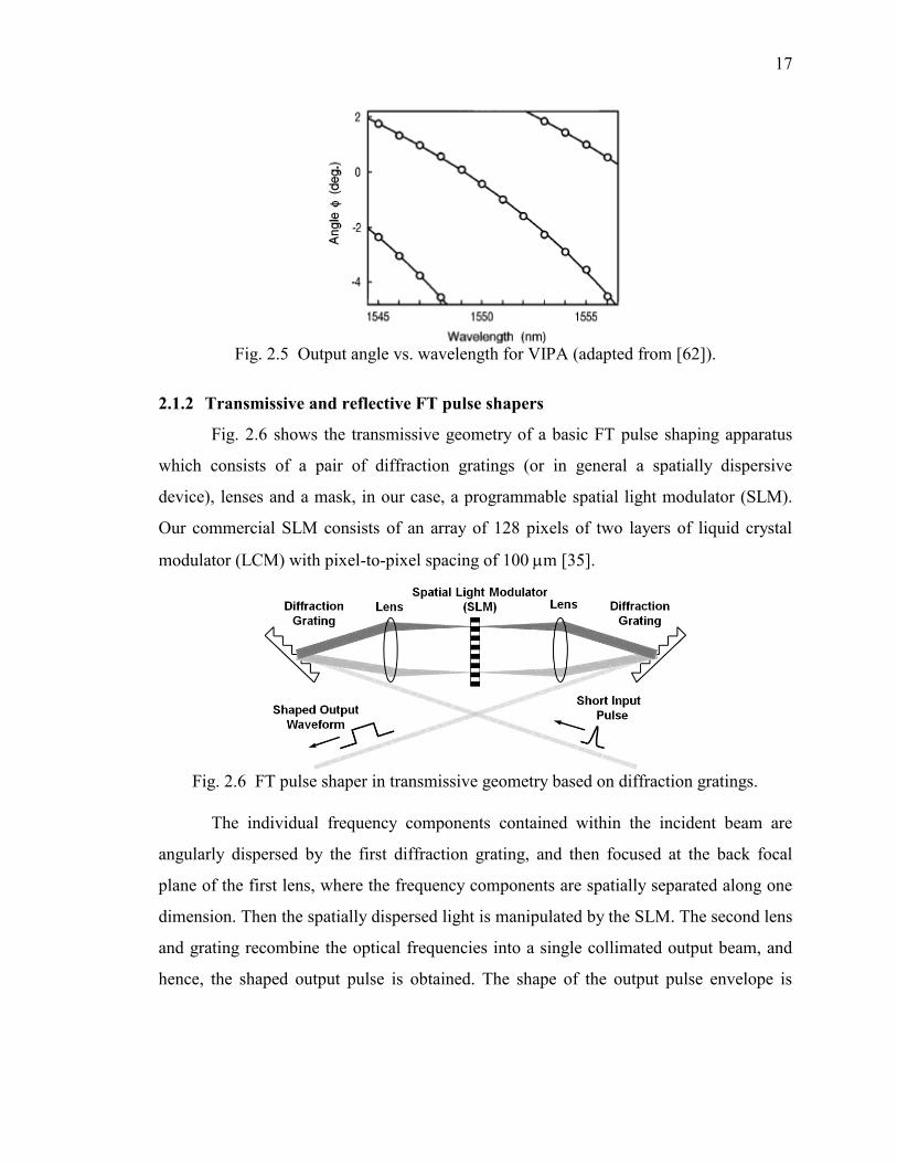
Fig. 2.6 shows the transmissive geometry of a basic FT pulse shaping apparatus
which consists of a pair of diffraction gratings (or in general a spatially dispersive
device), lenses and a mask, in our case, a programmable spatial light modulator (SLM).
Our commercial SLM consists of an array of 128 pixels of two layers of liquid crystal
modulator (LCM) with pixel-to-pixel spacing of 100 m [35].
Fig. 2.6 FT pulse shaper in transmissive geometry based on diffraction gratings.
The individual frequency components contained within the incident beam are
angularly dispersed by the first diffraction grating, and then focused at the back focal
plane of the first lens, where the frequency components are spatially separated along one
dimension. Then the spatially dispersed light is manipulated by the SLM. The second lens
and grating recombine the optical frequencies into a single collimated output beam, and
hence, the shaped output pulse is obtained. The shape of the output pulse envelope is
18
given by the Fourier transform of the pattern transferred by the masks onto the optical
spectrum.
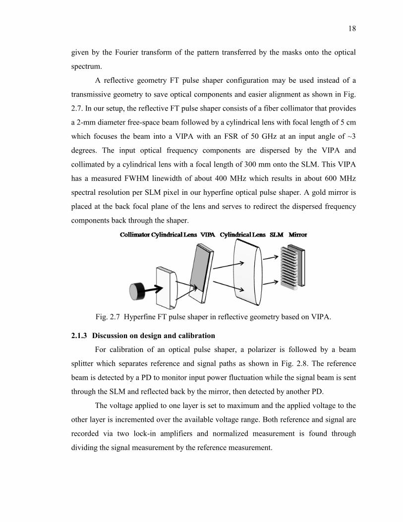
A reflective geometry FT pulse shaper configuration may be used instead of a
transmissive geometry to save optical components and easier alignment as shown in Fig.
2.7. In our setup, the reflective FT pulse shaper consists of a fiber collimator that provides
a 2-mm diameter free-space beam followed by a cylindrical lens with focal length of 5 cm
which focuses the beam into a VIPA with an FSR of 50 GHz at an input angle of ~3
degrees. The input optical frequency components are dispersed by the VIPA and
collimated by a cylindrical lens with a focal length of 300 mm onto the SLM. This VIPA
has a measured FWHM linewidth of about 400 MHz which results in about 600 MHz
spectral resolution per SLM pixel in our hyperfine optical pulse shaper. A gold mirror is
placed at the back focal plane of the lens and serves to redirect the dispersed frequency
components back through the shaper.
Fig. 2.7 Hyperfine FT pulse shaper in reflective geometry based on VIPA.
2.1.3 Discussion on design and calibration
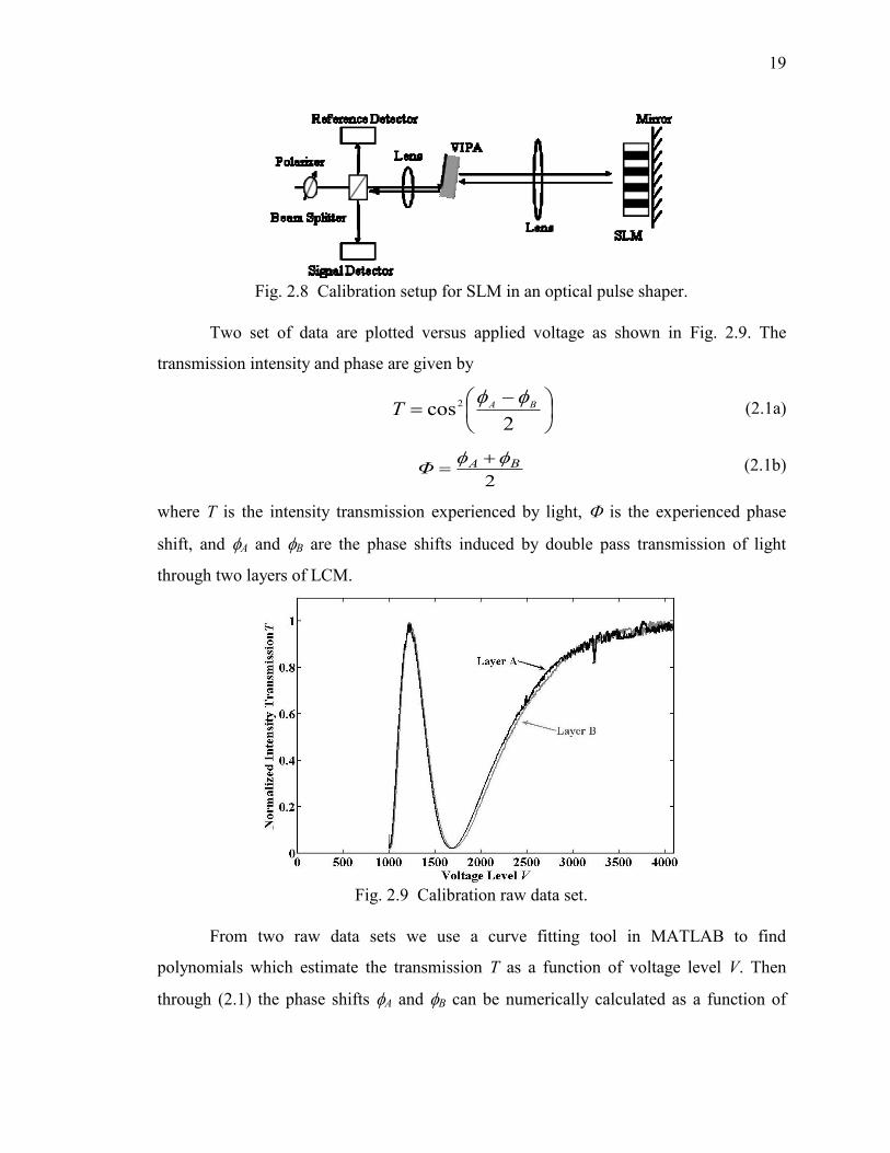
For calibration of an optical pulse shaper, a polarizer is followed by a beam
splitter which separates reference and signal paths as shown in Fig. 2.8. The reference
beam is detected by a PD to monitor input power fluctuation while the signal beam is sent
through the SLM and reflected back by the mirror, then detected by another PD.
The voltage applied to one layer is set to maximum and the applied voltage to the
other layer is incremented over the available voltage range. Both reference and signal are
recorded via two lock-in amplifiers and normalized measurement is found through
dividing the signal measurement by the reference measurement.
19
Fig. 2.8 Calibration setup for SLM in an optical pulse shaper.
Two set of data are plotted versus applied voltage as shown in Fig. 2.9. The
transmission intensity and phase are given by
2cos2 BAT
(2.1a)
2
BAΦ
(2.1b)
where T is the intensity transmission experienced by light, is the experienced phase
shift, and A and B are the phase shifts induced by double pass transmission of light
through two layers of LCM.
Fig. 2.9 Calibration raw data set.
From two raw data sets we use a curve fitting tool in MATLAB to find
polynomials which estimate the transmission T as a function of voltage level V. Then
through (2.1) the phase shifts A and B can be numerically calculated as a function of
20
voltage level V. To program an SLM for a given phase shift and transmission T we find
the corresponding phase shifts A and B using (2.1) and then we calculate the required
voltage levels.
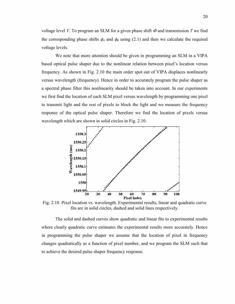
We note that more attention should be given in programming an SLM in a VIPA
based optical pulse shaper due to the nonlinear relation between pixel’s location versus
frequency. As shown in Fig. 2.10 the main order spot out of VIPA displaces nonlinearly
versus wavelength (frequency). Hence in order to accurately program the pulse shaper as
a spectral phase filter this nonlinearity should be taken into account. In our experiments
we first find the location of each SLM pixel versus wavelength by programming one pixel
to transmit light and the rest of pixels to block the light and we measure the frequency
response of the optical pulse shaper. Therefore we find the location of pixels versus
wavelength which are shown in solid circles in Fig. 2.10.
Fig. 2.10 Pixel location vs. wavelength. Experimental results, linear and quadratic curve
fits are in solid circles, dashed and solid lines respectively.
The solid and dashed curves show quadratic and linear fits to experimental results
where clearly quadratic curve estimates the experimental results more accurately. Hence
in programming the pulse shaper we assume that the location of pixel in frequency
changes quadratically as a function of pixel number, and we program the SLM such that
to achieve the desired pulse shaper frequency response.

21
2.2 RF Photonic Filter Based on Optical Pulse Shaping
The design and implementation of microwave photonic filters have been
investigated for many years [30]. These filters offer appealing features such as
programmability, tunability and broad bandwidth. Conventionally these filters are
designed based on multitap scheme which can be modeled as finite impulse response
(FIR) filters that will be discussed in details in chapter four. This technique has been used
to implement discrete time optical filters which perform as spectral amplitude filters.
Although little consideration has been given to spectral phase filters with an exception of
true-time delay lines which correspond to a controllable linear spectral phase for beam
forming in phased-array antennas [64].
Recently programmable RF photonic filters with arbitrary phase/amplitude
response were implemented via hyperfine resolution optical pulse shaping in [5, 9]. This
unveils a new approach for compression of spread-time electrical waveforms, in general,
and detection of spectrally encoded electrical waveforms, in particular, in ultra-broadband
wireless communication systems via matched filtering.
A schematic of RF photonic programmable waveform compressor/matched filter
is shown in Fig. 2.11 which is based on [9]. A tunable laser with a line-width below 0.1
pm centered at 1550.17 nm is input to a Lithium Niobate Mach-Zehnder (MZ) intensity
modulator (IM) with an electrical 3-dB BW of 30 GHz and a minimum transmission
voltage of V~4.75 V. A Mach-Zehnder intensity modulator is a two-arm interferometer
with 3-dB input splitter and 3-dB output coupler. We bias the modulator very close to its
minimum transmission and one of it arms is driven with an RF signal generated via the
RF photonic AWG that will be explained later. The importance of this biasing scheme is
explained in section 2.4.2. As a result, the output optical intensity is negligible when the
electrical input is zero, and for positive values of AC voltage input the optical carrier
electric field is modulated with electrical waveform so that the RF waveform maps
directly to the envelope of the optical carrier electric field. Modulating the optical carrier
with an RF electrical waveform in the MZ modulator transfers the RF signal into the
optical domain as a DSB modulation about the optical carrier. The resulting DSB
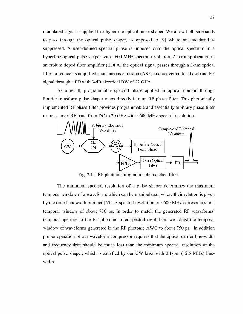
22
modulated signal is applied to a hyperfine optical pulse shaper. We allow both sidebands
to pass through the optical pulse shaper, as opposed to [9] where one sideband is
suppressed. A user-defined spectral phase is imposed onto the optical spectrum in a
hyperfine optical pulse shaper with ~600 MHz spectral resolution. After amplification in
an erbium doped fiber amplifier (EDFA) the optical signal passes through a 3-nm optical
filter to reduce its amplified spontaneous emission (ASE) and converted to a baseband RF
signal through a PD with 3-dB electrical BW of 22 GHz.
As a result, programmable spectral phase applied in optical domain through
Fourier transform pulse shaper maps directly into an RF phase filter. This photonically
implemented RF phase filter provides programmable and essentially arbitrary phase filter
response over RF band from DC to 20 GHz with ~600 MHz spectral resolution.
Fig. 2.11 RF photonic programmable matched filter.
The minimum spectral resolution of a pulse shaper determines the maximum
temporal window of a waveform, which can be manipulated, where their relation is given
by the time-bandwidth product [65]. A spectral resolution of ~600 MHz corresponds to a
temporal window of about 730 ps. In order to match the generated RF waveforms’
temporal aperture to the RF photonic filter spectral resolution, we adjust the temporal
window of waveforms generated in the RF photonic AWG to about 750 ps. In addition
proper operation of our waveform compressor requires that the optical carrier line-width
and frequency drift should be much less than the minimum spectral resolution of the
optical pulse shaper, which is satisfied by our CW laser with 0.1-pm (12.5 MHz) line-
width.
23
2.3 Matched Filtering Electrical Waveforms
In this section the experimental results are presented in which the matched filter
configuration in Fig. 2.10 is implemented and few examples of arbitrary waveforms are
generated and compressed by the application of spectral phase filtering. Before moving to
experimental results we discuss two approaches which we use to generate these ultra-
broadband arbitrary waveforms to test our matched filter. In following section we discuss
the first approach which is based on RF photonic AWG and in the second approach we
use the pattern generator from an Agilent N4901B Serial Bit Error Rate Tester, which we
program to generate periodically repeating binary patterns. The former approach provides
us with more complex waveforms considering the large dynamic range that voltage
amplitude can be programmed; however, the latter approach limits us to waveforms with
two level voltages, i.e. digital waveforms.
2.3.1 Generation of RF arbitrary waveforms
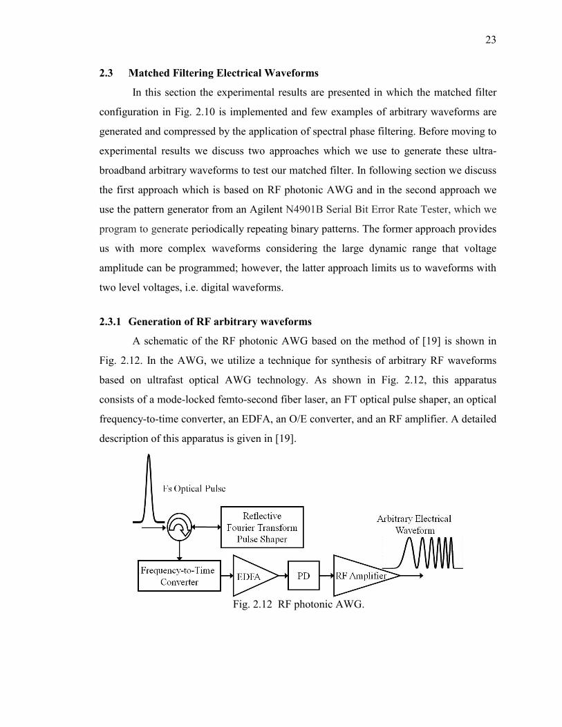
A schematic of the RF photonic AWG based on the method of [19] is shown in
Fig. 2.12. In the AWG, we utilize a technique for synthesis of arbitrary RF waveforms
based on ultrafast optical AWG technology. As shown in Fig. 2.12, this apparatus
consists of a mode-locked femto-second fiber laser, an FT optical pulse shaper, an optical
frequency-to-time converter, an EDFA, an O/E converter, and an RF amplifier. A detailed
description of this apparatus is given in [19].
Fig. 2.12 RF photonic AWG.
24
Ultra-short optical pulses from the mode-locked laser (~100 fs, 50 MHz repetition
rate) are spectrally filtered in the reflective-geometry FT optical pulse shaper which
enables to impose a user-defined optical filter function onto the power spectrum of the
optical pulses. The output pulses are dispersed in 1.6 km of SMF which uniquely maps
optical frequency to time and results in a temporal intensity profile which is a scaled
version of the filter function applied in the optical pulse shaper.
The output tailored optical intensity waveforms are converted to electrical signals
via O/E conversion in a PD with an electrical 3-dB BW of ~22 GHz. The RF electrical
output of the PD is amplified with a broadband RF amplifier (0.1-18 GHz, ~30-dB gain)
to be applied to an IM in the next stage. Currently we can achieve 0.7-V peak-to-peak
electrical waveforms.
The time aperture of the generated waveforms is determined by the optical
bandwidth and the length of the fiber stretcher. In our setup the length of the fiber
stretcher has been chosen 1.6 km in order to obtain waveforms with about 750-ps
temporal window which is the time aperture of the RF photonic filter setup.
2.3.2 Compression of chirp waveform
Fig. 2.13 shows matched filtering of an ultra-broadband RF electrical chirp
waveform. The chirp waveform is designed with a spectrum centered at ~7.5 GHz, a
~733 ps temporal window, and the fastest oscillation cycle corresponding to ~15 GHz.
Fig. 2.13(a) shows the pre-equalized RF chirp waveform synthesized via the RF photonic
AWG which is applied to the RF photonic filter. We pre-equalize the modulator electrical
input signal by generating its higher frequency content with stronger amplitude to
overcome the higher frequency roll-off of modulator, photodiode and pulse shaper
resulting in a uniform chirp at the RF photonic output when the pulse shaper is quiescent.
Fig. 2.13(b) shows the RF photonic filter output electrical waveform when the pulse
shaper is quiescent. As a result of the pre-equalization, the amplitude of the chirp
waveform in Fig. 2.13(b) is more uniform in time than the input chirp waveform in Fig.
2.13(a), and the individual oscillations have become sharper due to the squaring operation
of photodiode.
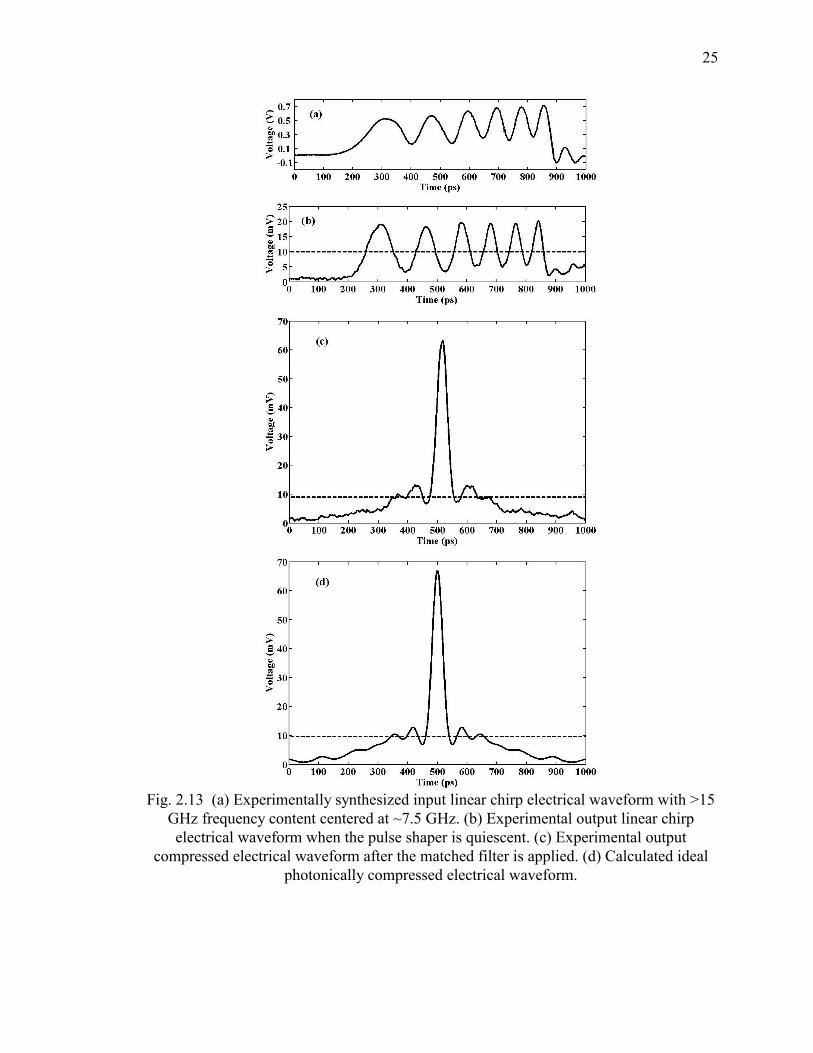
25
Fig. 2.13 (a) Experimentally synthesized input linear chirp electrical waveform with >15
GHz frequency content centered at ~7.5 GHz. (b) Experimental output linear chirp
electrical waveform when the pulse shaper is quiescent. (c) Experimental output
compressed electrical waveform after the matched filter is applied. (d) Calculated ideal
photonically compressed electrical waveform.
26
Fig. 2.13(c) shows the compressed electrical waveform at the output after the
conjugate spectral phase, i.e. the matched filter, is applied through the RF photonic filter.
A calculation of the electrical waveform of Fig. 2.13(b) processed through an ideal
conjugate spectral phase optical filter which is numerically performed through FFT in
MATLAB is shown in Fig. 2.13(d).
Here we give two definitions to compare the output uncompressed and
compressed voltage waveforms in order to evaluate the waveform compressor
performance. We define a gain parameter as the ratio of the compressed pulse peak
voltage, minus its DC level, to the uncompressed waveform peak voltage, minus its DC
level, all measured after the PD, as
uu
cc
DCV
DCV
(2.2)
where subscripts “c” and “u” denote “compressed” and “uncompressed” respectively.
can be expressed in decibels (dB) as
10log20)dB( (2.3)
Since a photodiode maps optical intensity to an electrical signal, the resulting
voltage signal is required to be a positive definite quantity and has a non-zero DC level.
The subtraction of the DC voltage is relevant since a DC voltage carries no information
and may be easily blocked by a DC blocker. We also define a compression factor as the
ratio of the uncompressed voltage waveform temporal window Tu to the compressed
voltage pulse FWHM duration tc, all measured after subtraction of their DC levels, as
c
u
t
T (2.4)
Note that the pulse FWHM duration is most meaningful for a waveform with no
DC level, and it gives a measure of frequency bandwidth for signals with no DC level.
Therefore the temporal pulse width has been measured after subtraction of the DC level,
which has information about frequency content of the pulse.
A 14.21-dB gain parameter has been achieved, and the output electrical voltage
pulse FWHM duration is 40 ps which corresponds to a compression factor of 18.3. For

27
the ideally matched filtered waveform, a 15.11-dB gain parameter and a 38-ps FWHM
electrical voltage pulse duration, which corresponds to a compression factor of 19.3, are
expected. In each trace Fig. 2.13 the dashed line shows the DC level of the PD output
voltage waveform averaged over its 733-ps temporal window from 148 to 880 ps. The
excellent agreement between experiment and simulation suggests that the uncompressed
RF waveform spectral phase is being corrected with a high degree of precision.
Fig. 2.14 (a) Calculated spectral phases of the waveforms in Fig. 2.13 (b) and (c) are
shown in squares and solid circles respectively. (b) Calculated spectral amplitudes of the
waveforms in Fig. 2.13 (b) and (c) are shown in squares and solid circles respectively.
The spectral phase and amplitude of the chirp waveform in Fig. 13(b) are
calculated through fast Fourier transform (FFT) and shown by squares in Fig. 2.14 (a), (b)
respectively. The large quadratic spectral phase is consistent with the linearly chirp
waveform design. Similarly the spectral phase and amplitude of the compressed
28
waveform are shown by solid circles in Fig. 2.14 (a), (b) respectively which show that the
spectral phase is compensated with an error less than 0.2 rad from DC to 15 GHz.
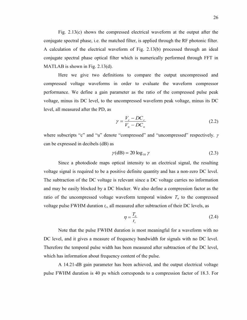
Fig. 2.15 (a) Output linear chirp electrical waveform with ~12.5 GHz BW centered at
~6.25 GHz when the pulse shaper is quiescent. (b) Output compressed electrical
waveform after the matched filter is applied. (c) Calculated ideally compressed electrical
waveform.
The slight difference between the uncompressed and compressed spectral
amplitudes is expected since the phase programming in SLM introduces some frequency

29
dependent loss which is due to the abrupt phase change between adjacent SLM pixels.
This effect has been studied in line-by-line pulse shaping [66].
Fig. 2.16 (a) Output linear chirp electrical waveform with ~10 GHz BW centered at ~5
GHz when the pulse shaper is quiescent. (b) Output compressed electrical waveform after
the matched filter is applied. (c) Calculated ideally compressed electrical waveform.
We have also performed waveform compression for ultra-broadband RF electrical
chirp waveforms similar to Fig. 2.13 for different frequency bandwidths where Fig. 2.15,
Fig. 2.16, and Fig. 2.17 show the results for linearly frequency-modulated electrical
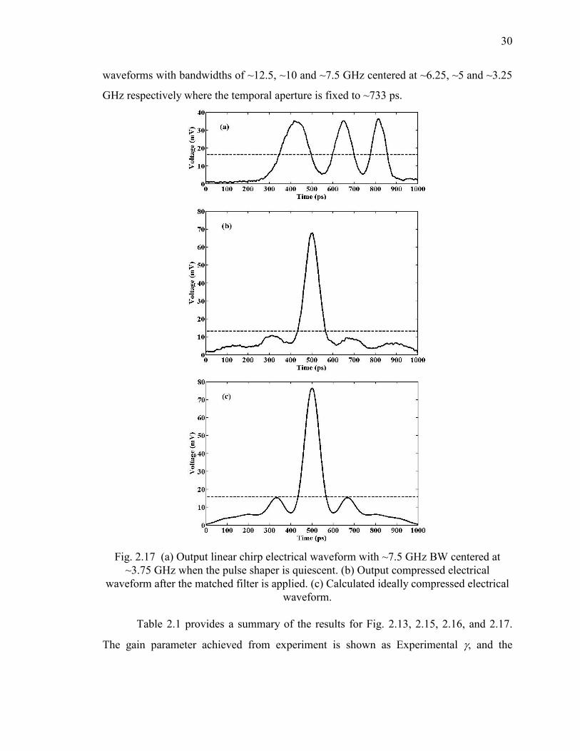
30
waveforms with bandwidths of ~12.5, ~10 and ~7.5 GHz centered at ~6.25, ~5 and ~3.25
GHz respectively where the temporal aperture is fixed to ~733 ps.
Fig. 2.17 (a) Output linear chirp electrical waveform with ~7.5 GHz BW centered at
~3.75 GHz when the pulse shaper is quiescent. (b) Output compressed electrical
waveform after the matched filter is applied. (c) Calculated ideally compressed electrical
waveform.
Table 2.1 provides a summary of the results for Fig. 2.13, 2.15, 2.16, and 2.17.
The gain parameter achieved from experiment is shown as Experimental , and the
31
calculated gain parameter after processing the chirp waveform through an ideal matched
filter is given as Numerical . The FWHM pulse duration of resultant compressed pulse
from experiment and after processing the chirp waveform through an ideal compressor
and also their corresponding compression factor are similarly given. Here also the
excellent agreement between experiment and simulation suggests that the uncompressed
RF electrical chirp waveforms are compressed with a high degree of precision.
Table 2.1 Experimental and numerical gain , FWHM duration, and compression factor
for chirp waveforms. Frequency
Bandwidth
(GHz)
Experimental
(dB)
Numerical
(dB)
Experimental
FWHM (ps)
Experimental
Numerical
FWHM
(ps)
Numerical
15 14.2 15.1 40 18.3 38 19.3
12.5 12 13 46 15.9 45 16.3
10 10.4 11.6 54 13.6 54 13.6
7.5 8.7 9.6 70 10.5 69 10.6
2.3.3 Compression of pseudorandom sequence waveform
Fig. 2.18 shows the matched filtering of a 15-chip PR code (001001101011110)
ultra-broadband RF electrical waveform at a chip rate corresponding to ~18.7 Gb/s with
~800-ps temporal window generated by the RF photonic AWG. Fig. 2.18(a) shows the
pre-equalized RF 15-chip PR waveform synthesized via the RF photonic AWG. Fig.
2.18(b) shows the RF photonic filter output electrical waveform when the pulse shaper
adds no spectral phase. The spectral phase and amplitude of the PR waveform are
calculated by FFT of the data in Fig. 2.18(b) and are shown by squares in Fig. 2.19. Fig.
2.18(c) shows the compressed electrical waveform at the PD output after the conjugate
spectral phase is applied. The spectral amplitude and phase of the compressed waveform
are shown by solid circles in Fig. 2.19 which show that the spectral phase is compensated
with an error less than 0.2 rad from DC to 15.5 GHz. A 14.07-dB gain parameter has been
achieved, and the output electrical voltage pulse FWHM duration is 50 ps which
corresponds to a compression factor of 16.
32
Fig. 2.18 (a) Experimentally synthesized input 15-chip PR electrical waveform. (b)
Experimental output 15-chip PR electrical waveform when the pulse shaper is quiescent.
(c) Experimental output compressed electrical waveform after the matched filter is
applied. (d) Calculated ideal photonically compressed electrical waveform.
A calculation of the electrical waveform of Fig. 2.18(b) processed through an
ideal conjugate spectral phase optical filter is shown in Fig. 2.18(d). For the ideally
33
matched filtered electrical waveform, a 14.85-dB gain parameter and a 46-ps FWHM
pulse duration, which corresponds to a compression factor of 17.4, are expected. Here
also the excellent agreement between experiment and simulation suggests that the
uncompressed RF electrical waveform is matched filtered with a high degree of precision.
Fig. 2.19 (a) Calculated spectral phases of the waveforms in Fig. 2.17 (b) and (c) are
shown in squares and solid circles respectively. (b) Calculated spectral amplitudes of the
waveforms in Fig. 2.17 (b) and (c) are shown in squares and solid circles respectively.
Using the second approach for generation of RF electrical waveforms we use the
pattern generator from a SerialBERT to generate a periodically repeating 15-chip PR
sequence (001001101011110) at 13.5 Gb/s. Fig. 2.20(a) shows the 15-chip PR electrical
waveform when the pulse shaper is quiescent. Fig. 2.20(b) shows the compressed
electrical waveform at the PD output after the conjugate spectral phase is applied. A 15.3-
34
dB gain parameter has been achieved, and the output electrical voltage pulse FWHM
duration is 53 ps which corresponds to a compression factor of 21.
Fig. 2.20 (a) Output periodic 15-chip PR sequence waveform at 13.5 Gb/s when the
pulse shaper is quiescent. (b) Output compressed electrical waveform after the matched
filter is applied. (c) Calculated ideally compressed electrical waveform.
A calculation of the electrical waveform of Fig. 2.20(a) processed through an ideal
conjugate spectral phase optical filter is shown in Fig. 2.20(c). For the ideally matched
filtered electrical waveform, a 15.9-dB gain parameter and a 51-ps FWHM pulse
duration, which corresponds to a compression factor of 21.8, are expected. Here also the
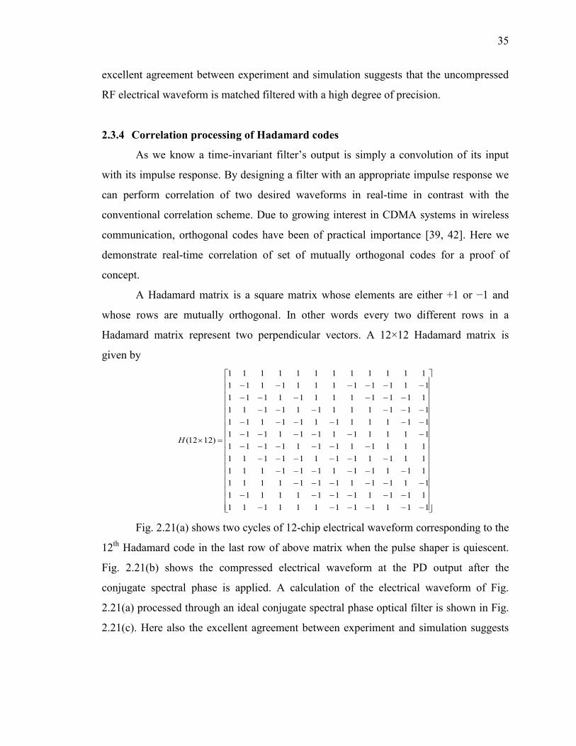
35
excellent agreement between experiment and simulation suggests that the uncompressed
RF electrical waveform is matched filtered with a high degree of precision.
2.3.4 Correlation processing of Hadamard codes
As we know a time-invariant filter’s output is simply a convolution of its input
with its impulse response. By designing a filter with an appropriate impulse response we
can perform correlation of two desired waveforms in real-time in contrast with the
conventional correlation scheme. Due to growing interest in CDMA systems in wireless
communication, orthogonal codes have been of practical importance [39, 42]. Here we
demonstrate real-time correlation of set of mutually orthogonal codes for a proof of
concept.
A Hadamard matrix is a square matrix whose elements are either +1 or −1 and
whose rows are mutually orthogonal. In other words every two different rows in a
Hadamard matrix represent two perpendicular vectors. A 12×12 Hadamard matrix is
given by
111111111111
111111111111
111111111111
111111111111
111111111111
111111111111
111111111111
111111111111
111111111111
111111111111
111111111111
111111111111
)1212(H
Fig. 2.21(a) shows two cycles of 12-chip electrical waveform corresponding to the
12th
Hadamard code in the last row of above matrix when the pulse shaper is quiescent.
Fig. 2.21(b) shows the compressed electrical waveform at the PD output after the
conjugate spectral phase is applied. A calculation of the electrical waveform of Fig.
2.21(a) processed through an ideal conjugate spectral phase optical filter is shown in Fig.
2.21(c). Here also the excellent agreement between experiment and simulation suggests

36
that the uncompressed RF electrical waveform is matched filtered with a high degree of
precision.
Now we generate twelve mutually orthogonal waveforms which are shown
consecutively in Fig. 2.22 as a solid line in using rows of the above matrix. We utilize our
matched filter to implement a filter with an impulse response matched to the 12th
Hadamard code waveform.
Fig. 2.21 (a) Output 12
th Hadamard code waveform at 13.5 Gb/s when the pulse shaper is
quiescent. (b) Output compressed electrical waveform after the matched filter is applied.
(c) Calculated ideally compressed electrical waveform.
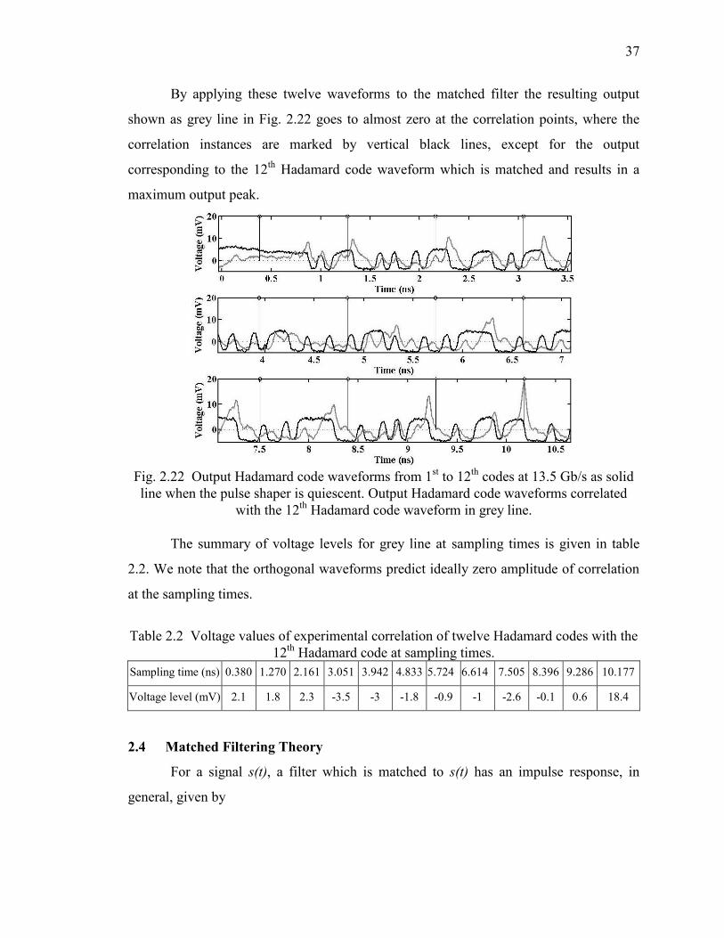
37
By applying these twelve waveforms to the matched filter the resulting output
shown as grey line in Fig. 2.22 goes to almost zero at the correlation points, where the
correlation instances are marked by vertical black lines, except for the output
corresponding to the 12th
Hadamard code waveform which is matched and results in a
maximum output peak.
Fig. 2.22 Output Hadamard code waveforms from 1
st to 12
th codes at 13.5 Gb/s as solid
line when the pulse shaper is quiescent. Output Hadamard code waveforms correlated
with the 12th
Hadamard code waveform in grey line.
The summary of voltage levels for grey line at sampling times is given in table
2.2. We note that the orthogonal waveforms predict ideally zero amplitude of correlation
at the sampling times.
Table 2.2 Voltage values of experimental correlation of twelve Hadamard codes with the
12th
Hadamard code at sampling times.
Sampling time (ns) 0.380 1.270 2.161 3.051 3.942 4.833 5.724 6.614 7.505 8.396 9.286 10.177
Voltage level (mV) 2.1 1.8 2.3 -3.5 -3 -1.8 -0.9 -1 -2.6 -0.1 0.6 18.4
2.4 Matched Filtering Theory
For a signal s(t), a filter which is matched to s(t) has an impulse response, in
general, given by
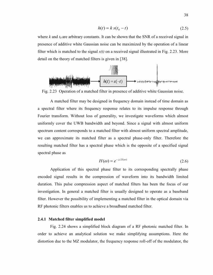
38
)()( 0 ttskth (2.5)
where k and t0 are arbitrary constants. It can be shown that the SNR of a received signal in
presence of additive white Gaussian noise can be maximized by the operation of a linear
filter which is matched to the signal s(t) on a received signal illustrated in Fig. 2.23. More
detail on the theory of matched filters is given in [38].
Fig. 2.23 Operation of a matched filter in presence of additive white Gaussian noise.
A matched filter may be designed in frequency domain instead of time domain as
a spectral filter where its frequency response relates to its impulse response through
Fourier transform. Without loss of generality, we investigate waveforms which almost
uniformly cover the UWB bandwidth and beyond. Since a signal with almost uniform
spectrum content corresponds to a matched filter with almost uniform spectral amplitude,
we can approximate its matched filter as a spectral phase-only filter. Therefore the
resulting matched filter has a spectral phase which is the opposite of a specified signal
spectral phase as
)()( SjeH (2.6)
Application of this spectral phase filter to its corresponding spectrally phase
encoded signal results in the compression of waveform into its bandwidth limited
duration. This pulse compression aspect of matched filters has been the focus of our
investigation. In general a matched filter is usually designed to operate as a baseband
filter. However the possibility of implementing a matched filter in the optical domain via
RF photonic filters enables us to achieve a broadband matched filter.
2.4.1 Matched filter simplified model
Fig. 2.24 shows a simplified block diagram of a RF photonic matched filter. In
order to achieve an analytical solution we make simplifying assumptions. Here the
distortion due to the MZ modulator, the frequency response roll-off of the modulator, the
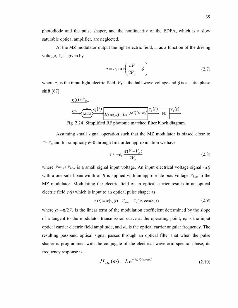
39
photodiode and the pulse shaper, and the nonlinearity of the EDFA, which is a slow
saturable optical amplifier, are neglected.
At the MZ modulator output the light electric field, e, as a function of the driving
voltage, V, is given by
V
Vee
2cos0 (2.7)
where e0 is the input light electric field, V is the half-wave voltage and is a static phase
shift [67].
Fig. 2.24 Simplified RF photonic matched filter block diagram.
Assuming small signal operation such that the MZ modulator is biased close to
V=V and for simplicity =0 through first order approximation we have
V
VVee
2
)(0
(2.8)
where V=vi+Vbias is a small signal input voltage. An input electrical voltage signal vi(t)
with a one-sided bandwidth of B is applied with an appropriate bias voltage Vbias to the
MZ modulator. Modulating the electric field of an optical carrier results in an optical
electric field ei(t) which is input to an optical pulse shaper as
)cos(])([)( 0 tωeVVtvte cbiasii (2.9)
where /2V is the linear term of the modulation coefficient determined by the slope
of a tangent to the modulator transmission curve at the operating point, e0 is the input
optical carrier electric field amplitude, and c is the optical carrier angular frequency. The
resulting passband optical signal passes through an optical filter that when the pulse
shaper is programmed with the conjugate of the electrical waveform spectral phase, its
frequency response is
)(
)( ciVj
MF eLH
(2.10)
40
where L accounts for the optical pulse shaper spectral loss which in general is a function
of angular frequency and in our pulse shaper it rolls off ~3 dB over a 20-GHz BW;
however, we approximate it as a constant. Further details on RF photonic filter spectral
amplitude are given in [5]. We can find the output optical electric field after passing
through the matched filter through Fourier transform as
)cos(]|})({|[
)}()({)(
1
0
1
tVVVeL
EHte
cbiasi
iMFo
F
F (2.11)
and when there is no spectral phase is added, the output electric field spectrum after
passing through the pulse shaper is simply
)cos(])([)()( 0 tωeVVtvLteLte cbiasiio (2.12)
A photodiode maps its input optical intensity to an electrical signal and it operates
as a square-law detector where its output electrical voltage signal is proportional to the
square of its input optical electric field
2)()( teκtv oo (2.13)
where is the O/E conversion coefficient. Thus from (2.11) we find the PD output
compressed electrical signal when the matched filter is applied as
212
0
22 ]|})({|[2
1)( VVVeLκtv biasio F (2.14)
The output uncompressed electrical signal, when the pulse shaper adds no spectral
phase, becomes
22
0
22 ])([2
1)( VVtveLκtv biasio (2.15)
2.4.2 Derivation of compression parameters
Following we briefly provide a simple analysis which describes the relation
between the gain parameter, the compression factor, and the bandwidth to characterize
the performance of a waveform compressor. We consider an electrical voltage signal vi(t)
with a spectrum uniformly equal to S0 from -B to B in the baseband and zero elsewhere.
The electrical signal spectral phase is assumed arbitrary; however, we are interested in a
spectral phase which spreads the signal vi(t) quite uniformly over its time aperture Tu. By

41
appropriately designing this spread-time waveform, the energy of the waveform may be
evenly spread over its time window. An arbitrary electrical waveform generated via the
RF photonic AWG is a definite positive voltage signal, since the photodiode has a
definite positive output voltage. Hence we assume the signal vi(t) takes definite positive
values over its temporal window and zero elsewhere. As a result the uncompressed
electrical signal vi(t) contains a positive DC voltage over its time aperture which is
uT
i
u
v dvT
DC0
)(1
(2.16)
We also assume that the signal vi(t) has a constant AC energy equal to U given by
uT
vi dDCvU0
2))(( (2.17)
where we can show through Parseval’s equation that
B
US
20
(2.18)
From foregoing assumptions we approximate
elsewhere 0
22for
)2sin(
|})({|01
uu
v
i
Tt
TDC
t
tBS
V
F (2.19)
Equation (2.19) is an approximation which roughly holds over the time aperture
of the signal from -Tu/2 to Tu/2. By substituting (2.19) in (2.11) we find an expression for
the output compressed electrical signal
2
0
2
0
22 )2sin(
2
1)(
VVDC
t
tBSeLtv biasvo
(2.20)
Then we find the compressed pulse peak voltage as
22
0
22 )2(2
1 VVDCBUeLV biasvc (2.21)
From (2.20), the DC level of the output compressed pulse over its temporal
window can be approximated. Here the DC level of the sinc function over the time
aperture Tu can be neglected compared to DCv when the time-bandwidth product TuB is
large. Then
42
22
0
22 )(2
1 VVDCeLDC biasvc (2.22)
The term Vbias-V can be made negligible by biasing the modulator close to its
minimum transmission. For an input electrical waveform that spreads extensively enough
over time the resulting output uncompressed signal DC voltage over its time window will
be much smaller than the output compressed waveform peak voltage, in other words
VVDCBU biasv 2 (2.23)
Thus we can show through (2.20) that the compressed pulse FWHM duration tc is
approximately given by
B
tc
44.0 (2.24)
Defining the maximum peak voltage of vi(t) as Vp, we write the output
uncompressed waveform peak voltage from (2.15) as
22
0
22 )(2
1 VVVeLV biaspu (2.25)
Finally by substituting in the gain parameter expression, we will obtain
uT
biasi
u
biasp
biasv
dVVvT
VVV
VVDCBUBU
0
22 ])([1
)(
)(222
(2.26)
In order to achieve further intuition in (2.26), we provide an approximate
analytical solution for a simple case. We assume vi(t) as a linear frequency-modulated
signal, which is long enough to span many frequency-modulation oscillations, as
elsewhere 0
22-
for 12
cos2)(
2
uuu
u
p
i
Tt
TTt
T
BV
tv (2.27)
If the signal time-bandwidth product is much larger than one, or in other words
there are many oscillations in the signal temporal window, then by approximating the DC
level and the ac energy of the signal, and the associated integrals, we can show
p
bias
p
bias
uuu
V
VV
V
VVBTBTBT
5
81
5
8
5
4
5
2
(2.28)
43
This expression shows that the theoretical gain parameter for a linear chirp signal
is decreasing by increasing Vbias-V and it takes its maximum value for Vbias=V which
corresponds to a bias point at the minimum transmission of the modulator. We note that
the low biasing of MZ modulator has been previously investigated to obtain high dynamic
range in photonic links [68].
We define the maximum gain parameter 0 as
BTBT uu5
4
5
20 (2.29)
By substituting for B we finally obtain
531.0176.00 (2.30)
Equations (2.29) and (2.30) show that for large values of compression factor, i. e.,
an input chirp waveform has a large time-bandwidth product, the maximum gain
parameter becomes approximately proportional to compression factor with a factor of
0.176. This expression gives us a rough estimate of an achievable gain parameter versus
compression factor. The foregoing analysis can also be performed through Fourier series
instead of Fourier transform that for completeness is given in Appendix A, which
precisely results in (2.28) for a periodic waveform with temporal window Tu set equal to
the repetition period Tr.
2.4.3 Comparison of experiment, simulation, and theory
The experimental and calculated gain parameters for compression of RF chirp
waveforms given in Table 2.1 are shown as a function of bandwidth of their frequency
content in Fig. 2.25. The circles illustrate the achieved gain parameter through
experiment. The squares show the gain parameter after processing the electrical chirp
waveforms through an ideal optical phase-only matched filter in simulation. The dashed
line shows the maximum theoretical gain parameter given by (2.29).
The difference between an ideal matched filter gain parameter and a theoretical
gain parameter predicted by (2.29) comes from the simplifying assumptions and
approximations that have been made in our derivation. Hence Fig. 2.25 illustrates the

44
behavior of an RF photonic matched filter performance which is in excellent agreement
with our experimental and numerical results.
Fig. 2.25 Gain parameter vs. frequency bandwidth for ultra-broadband RF chirp electrical
waveforms. The circles show the experimental gain parameter versus the frequency
corresponding to the chirp fastest oscillation cycle. The squares show the calculated gain
parameter after processing waveforms through an ideal photonically matched filter. The
dashed line shows the maximum theoretical gain parameter given by (2.29).
45
3. POST-COMPENSATION OF ANTENNA DISPERSION AND
ARBITRARY WAVEFORMS IDENTIFICATION
For the first time we demonstrate post-compensation of antenna dispersion using
RF photonic phase filters. We employ the technique discussed in chapter two to apply the
opposite of antennas nonlinear spectral phase to RF signals after a receiving antenna.
Therefore we are able to dispersion compensate a wireless antenna link.
In following first we describe how we measure an antenna impulse response by
exciting the antenna link with a very short electrical pulse, and we extract the spectral
phase of the antenna response by taking FFT. Then we compress the antenna link impulse
response to its bandwidth limited duration using an RF photonic phase filter. Further we
will demonstrate resolving different paths in a multipath environment and how this can
improve the performance of broadband radars. Finally we illustrate retrieval and
identification of user-defined waveforms transmitted over a wireless link by dispersion
compensation and matched filtering.
3.1 Antenna Dispersion
For large fractional bandwidth signals, the antennas utilized on both ends of a
wireless link may contribute very large dispersion to the receiving signal. While low
dispersion antennas exist, such as the planar bowtie or the ridged TEM, there are
frequency dependent antennas such as Archimedean spiral and log-periodic antennas.
From a bandwidth perspective, these represent appealing options for UWB systems. This
category of antennas although is known to introduce a strong frequency-dependent delay
to wideband signals, and provide examples of the effects of dispersion in UWB links.
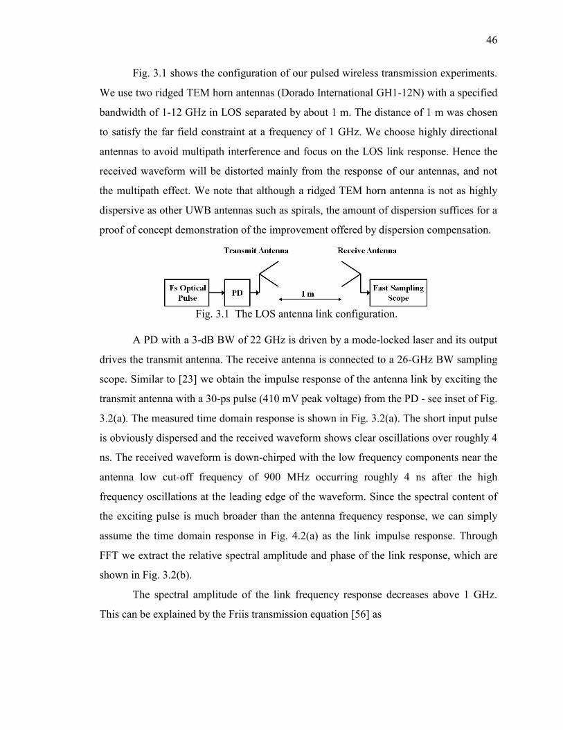
46
Fig. 3.1 shows the configuration of our pulsed wireless transmission experiments.
We use two ridged TEM horn antennas (Dorado International GH1-12N) with a specified
bandwidth of 1-12 GHz in LOS separated by about 1 m. The distance of 1 m was chosen
to satisfy the far field constraint at a frequency of 1 GHz. We choose highly directional
antennas to avoid multipath interference and focus on the LOS link response. Hence the
received waveform will be distorted mainly from the response of our antennas, and not
the multipath effect. We note that although a ridged TEM horn antenna is not as highly
dispersive as other UWB antennas such as spirals, the amount of dispersion suffices for a
proof of concept demonstration of the improvement offered by dispersion compensation.
Fig. 3.1 The LOS antenna link configuration.
A PD with a 3-dB BW of 22 GHz is driven by a mode-locked laser and its output
drives the transmit antenna. The receive antenna is connected to a 26-GHz BW sampling
scope. Similar to [23] we obtain the impulse response of the antenna link by exciting the
transmit antenna with a 30-ps pulse (410 mV peak voltage) from the PD - see inset of Fig.
3.2(a). The measured time domain response is shown in Fig. 3.2(a). The short input pulse
is obviously dispersed and the received waveform shows clear oscillations over roughly 4
ns. The received waveform is down-chirped with the low frequency components near the
antenna low cut-off frequency of 900 MHz occurring roughly 4 ns after the high
frequency oscillations at the leading edge of the waveform. Since the spectral content of
the exciting pulse is much broader than the antenna frequency response, we can simply
assume the time domain response in Fig. 4.2(a) as the link impulse response. Through
FFT we extract the relative spectral amplitude and phase of the link response, which are
shown in Fig. 3.2(b).
The spectral amplitude of the link frequency response decreases above 1 GHz.
This can be explained by the Friis transmission equation [56] as
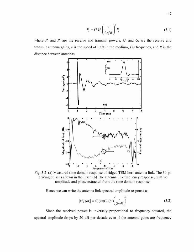
47
trtr PfR
vGGP
2
4
(3.1)
where Pr and Pt are the receive and transmit powers, Gr and Gt are the receive and
transmit antenna gains, v is the speed of light in the medium, f is frequency, and R is the
distance between antennas.
Fig. 3.2 (a) Measured time domain response of ridged TEM horn antenna link. The 30-ps
driving pulse is shown in the inset. (b) The antenna link frequency response, relative
amplitude and phase extracted from the time domain response.
Hence we can write the antenna link spectral amplitude response as
2
2)()()(
R
vGGH rtL
(3.2)
Since the received power is inversely proportional to frequency squared, the
spectral amplitude drops by 20 dB per decade even if the antenna gains are frequency
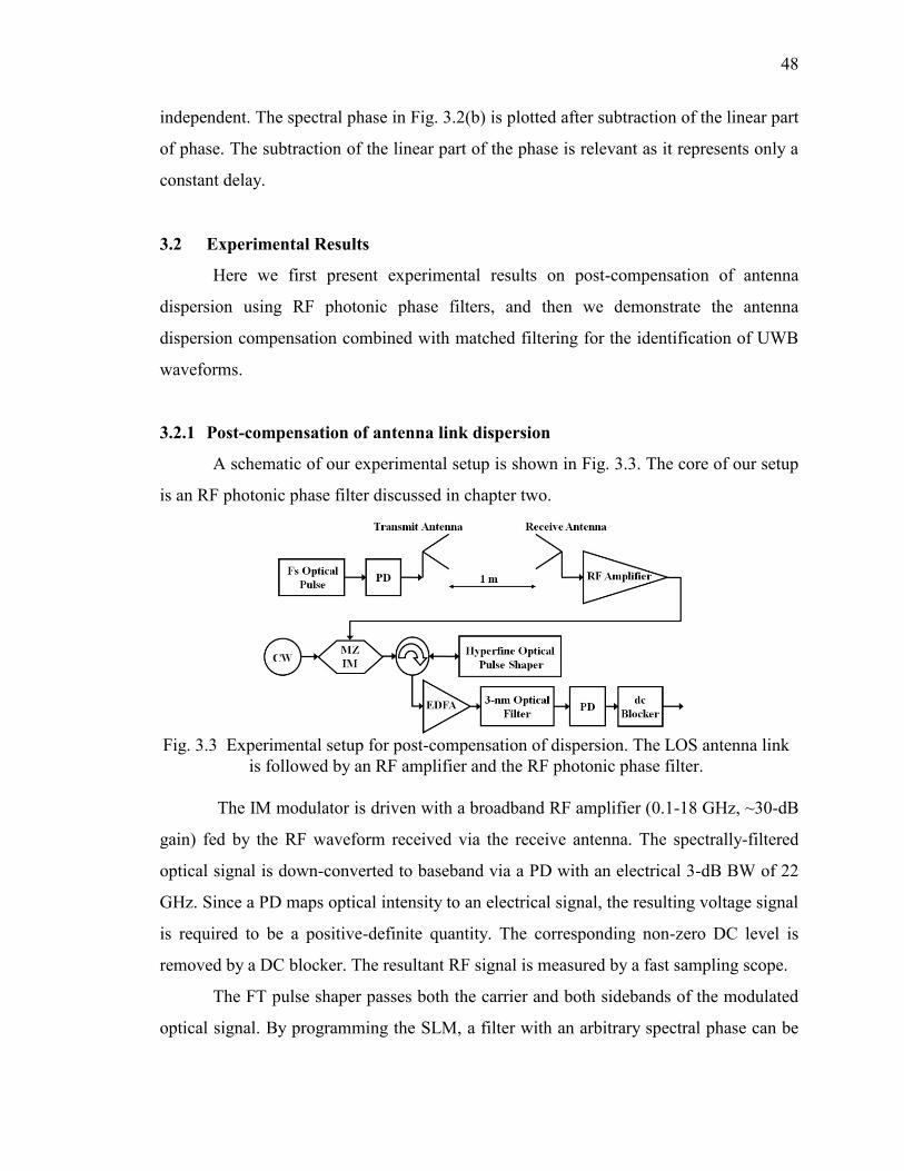
48
independent. The spectral phase in Fig. 3.2(b) is plotted after subtraction of the linear part
of phase. The subtraction of the linear part of the phase is relevant as it represents only a
constant delay.
3.2 Experimental Results
Here we first present experimental results on post-compensation of antenna
dispersion using RF photonic phase filters, and then we demonstrate the antenna
dispersion compensation combined with matched filtering for the identification of UWB
waveforms.
3.2.1 Post-compensation of antenna link dispersion
A schematic of our experimental setup is shown in Fig. 3.3. The core of our setup
is an RF photonic phase filter discussed in chapter two.
Fig. 3.3 Experimental setup for post-compensation of dispersion. The LOS antenna link
is followed by an RF amplifier and the RF photonic phase filter.
The IM modulator is driven with a broadband RF amplifier (0.1-18 GHz, ~30-dB
gain) fed by the RF waveform received via the receive antenna. The spectrally-filtered
optical signal is down-converted to baseband via a PD with an electrical 3-dB BW of 22
GHz. Since a PD maps optical intensity to an electrical signal, the resulting voltage signal
is required to be a positive-definite quantity. The corresponding non-zero DC level is
removed by a DC blocker. The resultant RF signal is measured by a fast sampling scope.
The FT pulse shaper passes both the carrier and both sidebands of the modulated
optical signal. By programming the SLM, a filter with an arbitrary spectral phase can be
49
synthesized and imposed on the optical signal. After O/E conversion, the relation between
input and output electrical signals is given by
)()()( iFo VHV (3.3)
where HF() is the RF photonic filter frequency response, and Vi() and Vo() are the
Fourier transforms of input and output electrical signals. For practical signals which are
real, one sideband is a complex-conjugate of the other. Thus, in our apparatus optical
phase filters are programmed with complex-conjugate symmetry about the optical carrier
frequency. In order to program the RF photonic filter as a phase-only filter we first extract
the spectrum of the output dispersed electrical waveform when the pulse shaper is
quiescent, i.e., no spectral phase is added, by taking FFT of the measured output
waveform. By imposing the opposite of the output dispersed waveform’s spectral phase
onto the corresponding optical signal spectrum, the envelope of the optical carrier electric
field is compressed to its transform-limited duration. This results in an electrical pulse
that is compressed to the bandwidth limited duration after O/E conversion. In other words
we have HF()=exp[-j<Vi()], which results in an output electrical signal with spectrum
)()()()(
ii
Vj
o VVeV i (3.4)
The results of antenna link dispersion compensation are shown in Fig. 3.4, where
voltage profiles after the DC blocker of Fig. 3.3 are plotted. Fig. 3.4(a) shows the output
waveform when the pulse shaper is quiescent. The output waveform after the RF photonic
filter when no spectral phase is added is almost the same as the received dispersed
waveform in Fig. 3.2(a). Then the spectral phase of the waveform in Fig. 3.4(a) is
extracted via FFT, and the SLM in the pulse shaper is programmed for equal but opposite
spectral phase. Mathematically we have HF()=exp[-j<HL()] which results in
)()(
)()()()(
iL
iL
Hj
o
VH
VHeV L
(3.5)
Assuming an input bandwidth limited pulse with a bandwidth larger than the link
bandwidth, the output signal Vo() becomes proportional to |HL()| with a constant factor.
Fig. 3.4(b) shows the compressed electrical waveform at the output after the conjugate
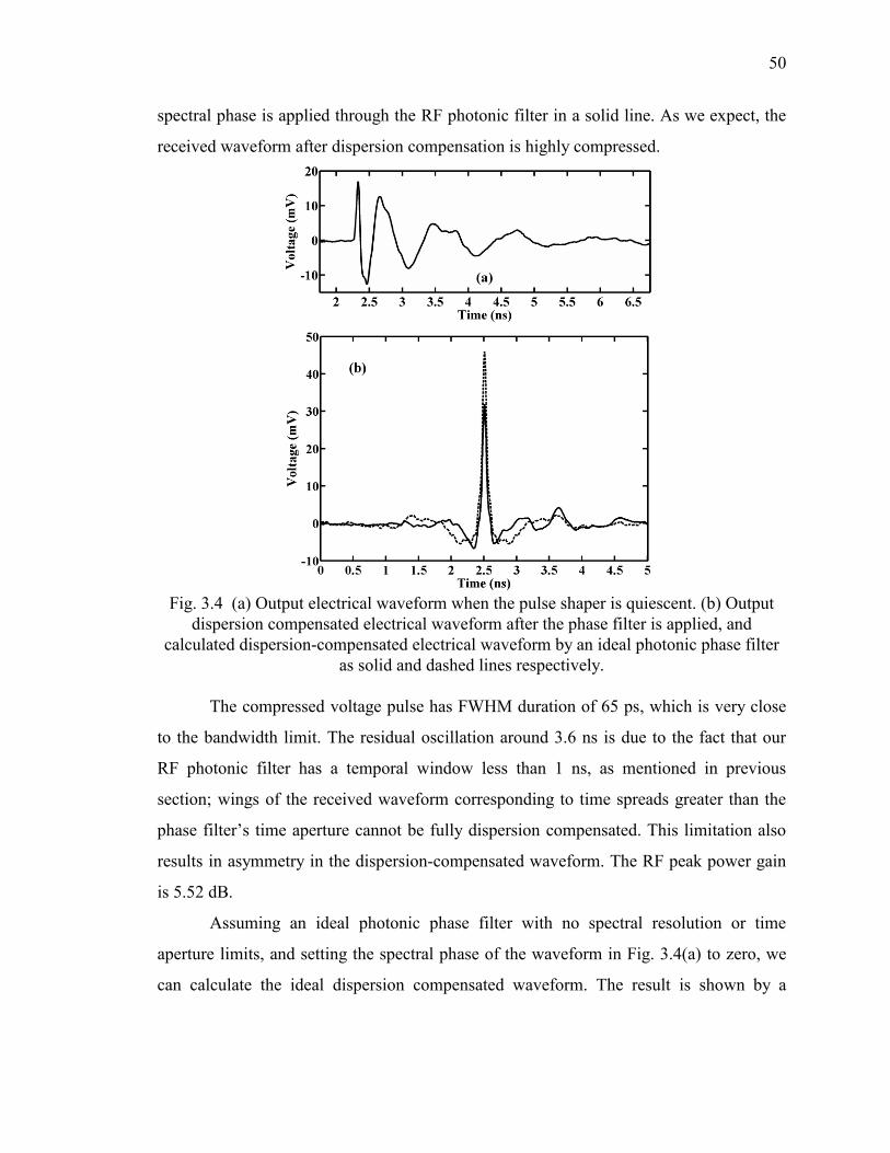
50
spectral phase is applied through the RF photonic filter in a solid line. As we expect, the
received waveform after dispersion compensation is highly compressed.
Fig. 3.4 (a) Output electrical waveform when the pulse shaper is quiescent. (b) Output
dispersion compensated electrical waveform after the phase filter is applied, and
calculated dispersion-compensated electrical waveform by an ideal photonic phase filter
as solid and dashed lines respectively.
The compressed voltage pulse has FWHM duration of 65 ps, which is very close
to the bandwidth limit. The residual oscillation around 3.6 ns is due to the fact that our
RF photonic filter has a temporal window less than 1 ns, as mentioned in previous
section; wings of the received waveform corresponding to time spreads greater than the
phase filter’s time aperture cannot be fully dispersion compensated. This limitation also
results in asymmetry in the dispersion-compensated waveform. The RF peak power gain
is 5.52 dB.
Assuming an ideal photonic phase filter with no spectral resolution or time
aperture limits, and setting the spectral phase of the waveform in Fig. 3.4(a) to zero, we
can calculate the ideal dispersion compensated waveform. The result is shown by a
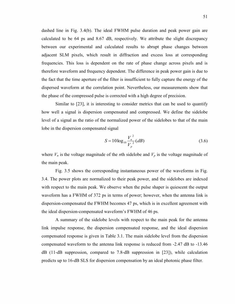
51
dashed line in Fig. 3.4(b). The ideal FWHM pulse duration and peak power gain are
calculated to be 64 ps and 8.67 dB, respectively. We attribute the slight discrepancy
between our experimental and calculated results to abrupt phase changes between
adjacent SLM pixels, which result in diffraction and excess loss at corresponding
frequencies. This loss is dependent on the rate of phase change across pixels and is
therefore waveform and frequency dependent. The difference in peak power gain is due to
the fact that the time aperture of the filter is insufficient to fully capture the energy of the
dispersed waveform at the correlation point. Nevertheless, our measurements show that
the phase of the compressed pulse is corrected with a high degree of precision.
Similar to [23], it is interesting to consider metrics that can be used to quantify
how well a signal is dispersion compensated and compressed. We define the sidelobe
level of a signal as the ratio of the normalized power of the sidelobes to that of the main
lobe in the dispersion compensated signal
)(log102
2
10 dBV
VS
p
n (3.6)
where Vn is the voltage magnitude of the nth sidelobe and Vp is the voltage magnitude of
the main peak.
Fig. 3.5 shows the corresponding instantaneous power of the waveforms in Fig.
3.4. The power plots are normalized to their peak power, and the sidelobes are indexed
with respect to the main peak. We observe when the pulse shaper is quiescent the output
waveform has a FWHM of 372 ps in terms of power; however, when the antenna link is
dispersion-compensated the FWHM becomes 47 ps, which is in excellent agreement with
the ideal dispersion-compensated waveform’s FWHM of 46 ps.
A summary of the sidelobe levels with respect to the main peak for the antenna
link impulse response, the dispersion compensated response, and the ideal dispersion
compensated response is given in Table 3.1. The main sidelobe level from the dispersion
compensated waveform to the antenna link response is reduced from -2.47 dB to -13.46
dB (11-dB suppression, compared to 7.8-dB suppression in [23]), while calculation
predicts up to 16-dB SLS for dispersion compensation by an ideal photonic phase filter.
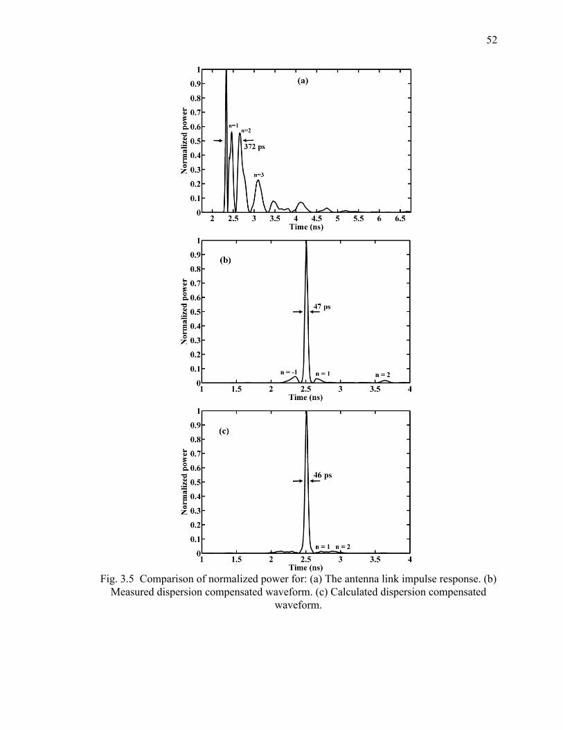
52
Fig. 3.5 Comparison of normalized power for: (a) The antenna link impulse response. (b)
Measured dispersion compensated waveform. (c) Calculated dispersion compensated
waveform.
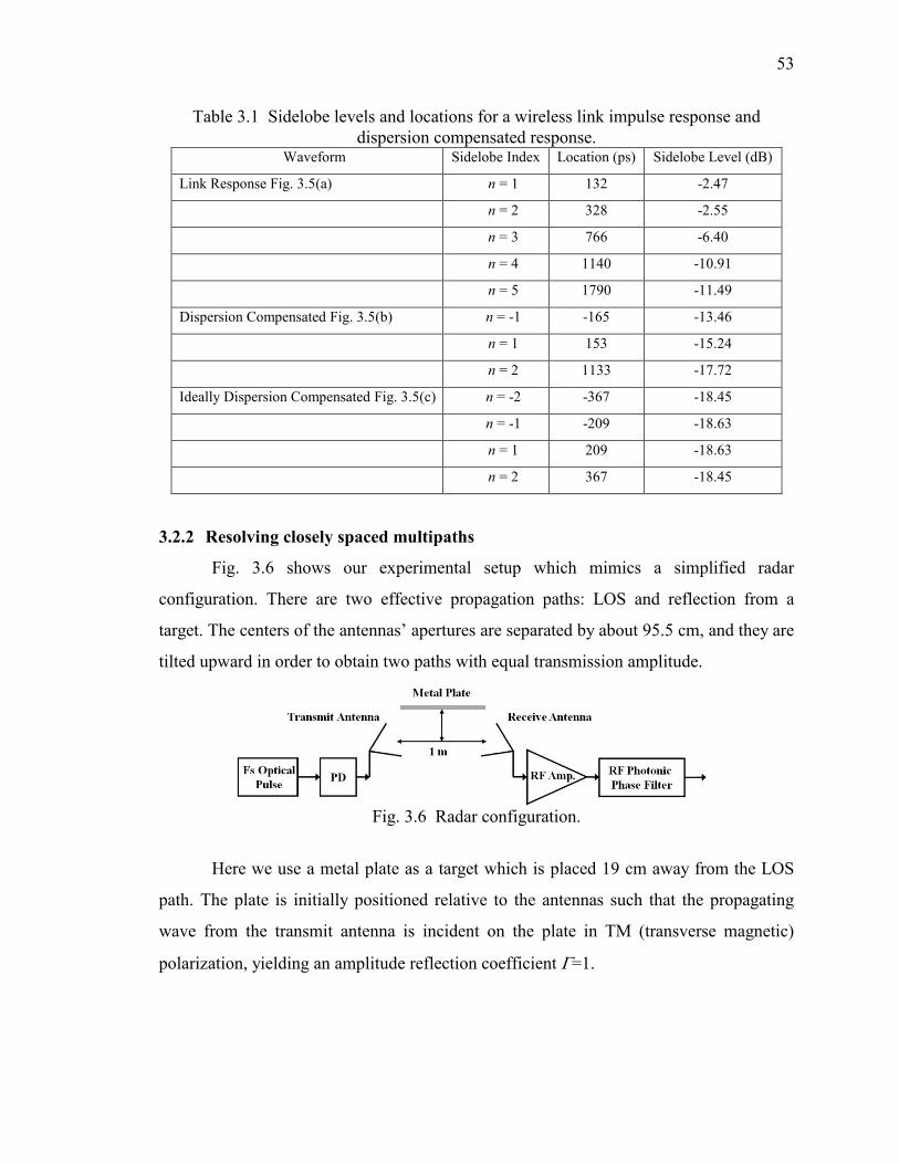
53
Table 3.1 Sidelobe levels and locations for a wireless link impulse response and
dispersion compensated response. Waveform Sidelobe Index Location (ps) Sidelobe Level (dB)
Link Response Fig. 3.5(a) n = 1 132 -2.47
n = 2 328 -2.55
n = 3 766 -6.40
n = 4 1140 -10.91
n = 5 1790 -11.49
Dispersion Compensated Fig. 3.5(b) n = -1 -165 -13.46
n = 1 153 -15.24
n = 2 1133 -17.72
Ideally Dispersion Compensated Fig. 3.5(c) n = -2 -367 -18.45
n = -1 -209 -18.63
n = 1 209 -18.63
n = 2 367 -18.45
3.2.2 Resolving closely spaced multipaths
Fig. 3.6 shows our experimental setup which mimics a simplified radar
configuration. There are two effective propagation paths: LOS and reflection from a
target. The centers of the antennas’ apertures are separated by about 95.5 cm, and they are
tilted upward in order to obtain two paths with equal transmission amplitude.
Fig. 3.6 Radar configuration.
Here we use a metal plate as a target which is placed 19 cm away from the LOS
path. The plate is initially positioned relative to the antennas such that the propagating
wave from the transmit antenna is incident on the plate in TM (transverse magnetic)
polarization, yielding an amplitude reflection coefficient =1.
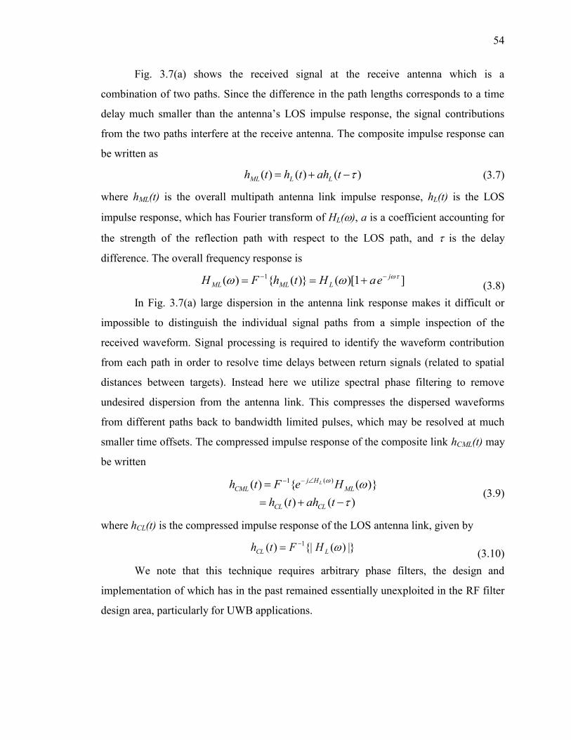
54
Fig. 3.7(a) shows the received signal at the receive antenna which is a
combination of two paths. Since the difference in the path lengths corresponds to a time
delay much smaller than the antenna’s LOS impulse response, the signal contributions
from the two paths interfere at the receive antenna. The composite impulse response can
be written as
)()()( tahthth LLML (3.7)
where hML(t) is the overall multipath antenna link impulse response, hL(t) is the LOS
impulse response, which has Fourier transform of HL(), a is a coefficient accounting for
the strength of the reflection path with respect to the LOS path, and is the delay
difference. The overall frequency response is
]1)[()}({)( 1 j
LMLML eaHthFH (3.8)
In Fig. 3.7(a) large dispersion in the antenna link response makes it difficult or
impossible to distinguish the individual signal paths from a simple inspection of the
received waveform. Signal processing is required to identify the waveform contribution
from each path in order to resolve time delays between return signals (related to spatial
distances between targets). Instead here we utilize spectral phase filtering to remove
undesired dispersion from the antenna link. This compresses the dispersed waveforms
from different paths back to bandwidth limited pulses, which may be resolved at much
smaller time offsets. The compressed impulse response of the composite link hCML(t) may
be written
)()(
)}({)()(1
tahth
HeFth
CLCL
ML
Hj
CMLL
(3.9)
where hCL(t) is the compressed impulse response of the LOS antenna link, given by
|})({|)( 1 LCL HFth
(3.10)
We note that this technique requires arbitrary phase filters, the design and
implementation of which has in the past remained essentially unexploited in the RF filter
design area, particularly for UWB applications.
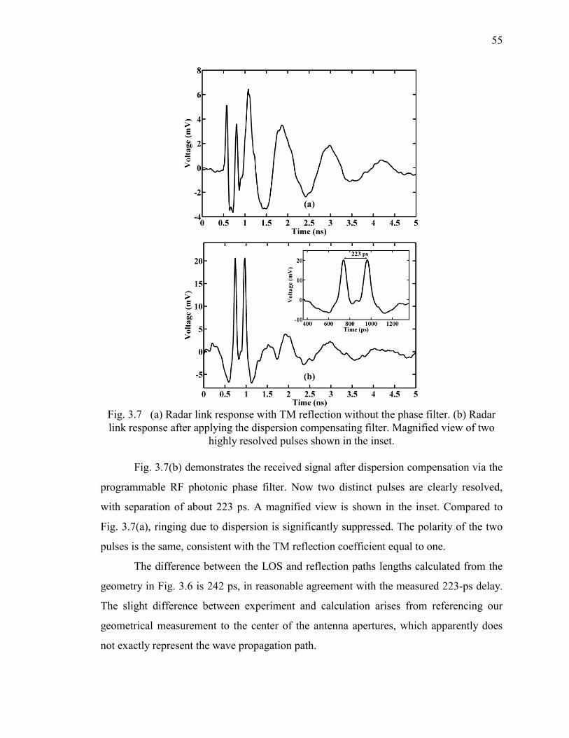
55
Fig. 3.7 (a) Radar link response with TM reflection without the phase filter. (b) Radar
link response after applying the dispersion compensating filter. Magnified view of two
highly resolved pulses shown in the inset.
Fig. 3.7(b) demonstrates the received signal after dispersion compensation via the
programmable RF photonic phase filter. Now two distinct pulses are clearly resolved,
with separation of about 223 ps. A magnified view is shown in the inset. Compared to
Fig. 3.7(a), ringing due to dispersion is significantly suppressed. The polarity of the two
pulses is the same, consistent with the TM reflection coefficient equal to one.
The difference between the LOS and reflection paths lengths calculated from the
geometry in Fig. 3.6 is 242 ps, in reasonable agreement with the measured 223-ps delay.
The slight difference between experiment and calculation arises from referencing our
geometrical measurement to the center of the antenna apertures, which apparently does
not exactly represent the wave propagation path.
56
Fig. 3.8 (a) Radar link response with TE reflection without the phase filter. (b) Radar
link response after applying the dispersion compensating filter.
We performed a similar experiment with the apparatus repositioned such that the
wave incident on the metal plate is in TE (transverse electric) polarization, which has a
reflection coefficient equal to minus one (=-1). Here the centers of the antenna apertures
are separated by about 92 cm and the metal plate is placed 26 cm away from the LOS.
Fig. 3.8(a) shows the received signal arising from the combination of the two paths
without dispersion compensation. Fig. 3.8(b) shows the received signal after dispersion
compensation via the programmable RF photonic phase filter. We observe two highly
resolved pulses separated by about 490 ps. The polarities of the two pulses are opposite,
as expected for TE reflection.

57
Summarizing the results of this section: we have demonstrated pulse compression
over UWB bandwidths, yielding distance resolution proportional to the bandwidth limited
pulse duration. This significantly improves on results without dispersion compensation,
where resolution is significantly degraded.
3.2.3 Identification of PR sequence over an antenna link
As mentioned, the application of UWB spread-time waveforms instead of
monopulses may be used to enhance transmit energy from a peak voltage limited
transmitter; however, utilizing a phase filter to realize pulse compression becomes
necessary. Spread-time waveforms may also be employed in UWB wireless
communication, for purposes of multi-access for example [42].
Here we utilize the programmable RF photonic phase filter both to dispersion
compensate the antenna link and simultaneously to compress a specific spread-time
waveform. This is achieved by programming the filter to apply the conjugate of the sum
of the antenna link spectral phase and the spread-time waveform spectral phase. Hence by
transmitting the spread-time waveform from the transmit antenna, we will obtain a
compressed pulse at the output of the RF photonic phase filter corresponding to each path
from the transmit antenna to the receive antenna. Compression of the spread-time
waveform at the receiver should also provide gain in RF peak power and improve the
SNR.
Fig. 3.9 shows the experimental setup, which is similar to the LOS setup of Fig.
3.3, but with a pattern generator providing the input electrical signal. Here we use the
pattern generator from an Agilent N4901B Serial Bit Error Rate Tester, which we
program to generate a periodically repeating PR sequence of 15-chip length
(000100110101111) at 13.5 Gb/s.
Fig. 3.10(a) shows two cycles of the pattern generator output. The waveform
observed at the receive antenna is shown as a solid line in Fig. 3.10(b). The dashed line
shows the simulation result, calculated by convolving the pattern generator output with
the antenna link impulse response
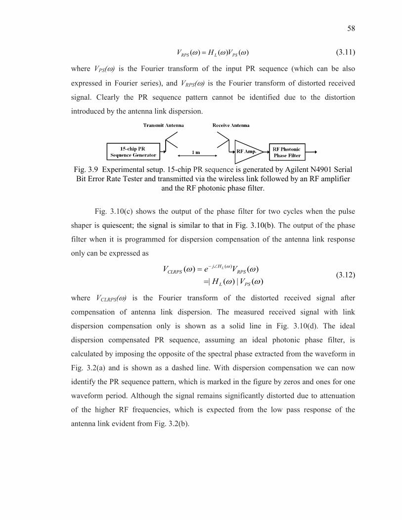
58
)()()( PSLRPS VHV
(3.11)
where VPS() is the Fourier transform of the input PR sequence (which can be also
expressed in Fourier series), and VRPS() is the Fourier transform of distorted received
signal. Clearly the PR sequence pattern cannot be identified due to the distortion
introduced by the antenna link dispersion.
Fig. 3.9 Experimental setup. 15-chip PR sequence is generated by Agilent N4901 Serial
Bit Error Rate Tester and transmitted via the wireless link followed by an RF amplifier
and the RF photonic phase filter.
Fig. 3.10(c) shows the output of the phase filter for two cycles when the pulse
shaper is quiescent; the signal is similar to that in Fig. 3.10(b). The output of the phase
filter when it is programmed for dispersion compensation of the antenna link response
only can be expressed as
)(|)(|
)()()(
PSL
RPS
Hj
CLRPS
VH
VeV L
(3.12)
where VCLRPS() is the Fourier transform of the distorted received signal after
compensation of antenna link dispersion. The measured received signal with link
dispersion compensation only is shown as a solid line in Fig. 3.10(d). The ideal
dispersion compensated PR sequence, assuming an ideal photonic phase filter, is
calculated by imposing the opposite of the spectral phase extracted from the waveform in
Fig. 3.2(a) and is shown as a dashed line. With dispersion compensation we can now
identify the PR sequence pattern, which is marked in the figure by zeros and ones for one
waveform period. Although the signal remains significantly distorted due to attenuation
of the higher RF frequencies, which is expected from the low pass response of the
antenna link evident from Fig. 3.2(b).

59
Fig. 3.10 (a) Generated PR sequence waveform. (b) Experimental and simulated
distorted PR sequence received through the antenna link as solid and dashed lines
respectively. (c) Output of the RF photonic filter when the pulse shaper is quiescent. (d)
Experimental and simulated retrieved PR sequence after compensating the antenna link
dispersion as solid and dashed lines respectively. (e) Experimental and simulated received
waveform after compensating the antenna link dispersion and conjugate phase filtering
the PR sequence waveform in solid and dashed lines respectively.
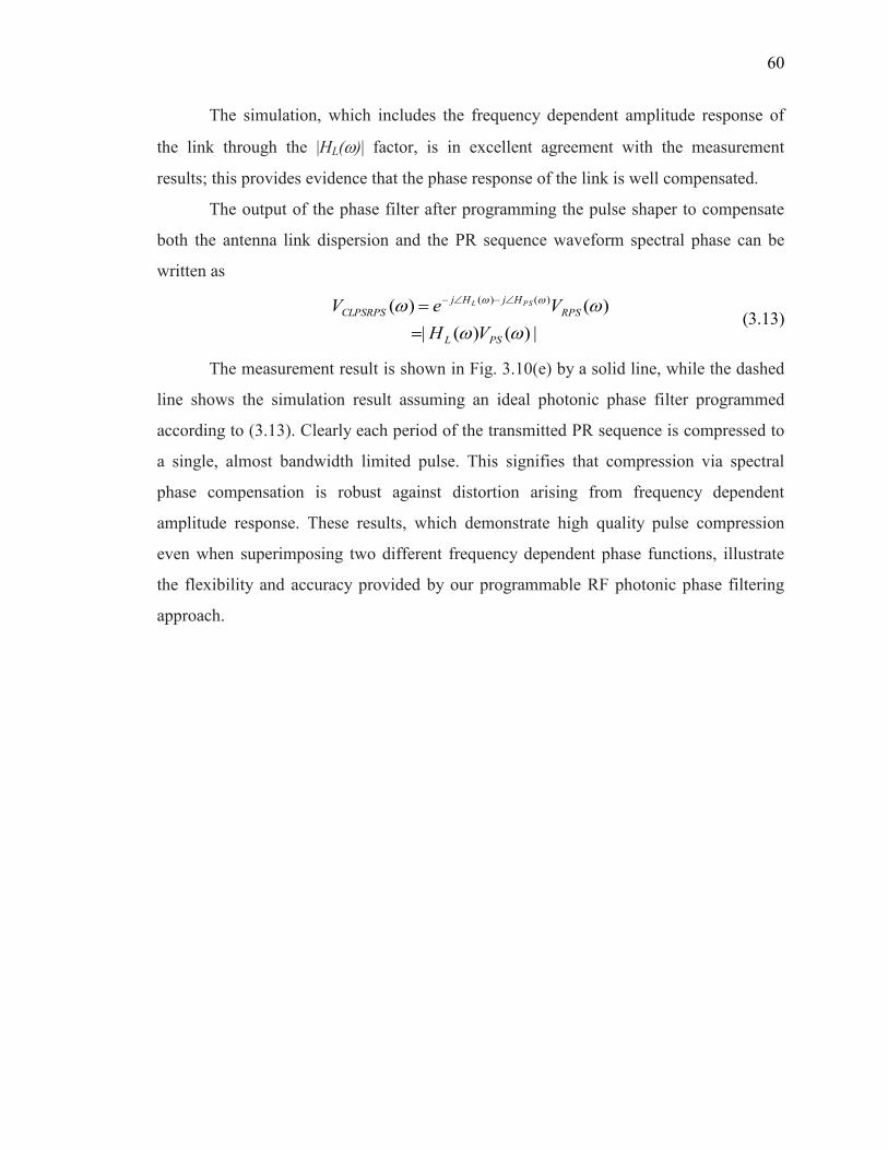
60
The simulation, which includes the frequency dependent amplitude response of
the link through the |HL()| factor, is in excellent agreement with the measurement
results; this provides evidence that the phase response of the link is well compensated.
The output of the phase filter after programming the pulse shaper to compensate
both the antenna link dispersion and the PR sequence waveform spectral phase can be
written as
|)()(|
)()()()(
PSL
RPS
HjHj
CLPSRPS
VH
VeV PSL
(3.13)
The measurement result is shown in Fig. 3.10(e) by a solid line, while the dashed
line shows the simulation result assuming an ideal photonic phase filter programmed
according to (3.13). Clearly each period of the transmitted PR sequence is compressed to
a single, almost bandwidth limited pulse. This signifies that compression via spectral
phase compensation is robust against distortion arising from frequency dependent
amplitude response. These results, which demonstrate high quality pulse compression
even when superimposing two different frequency dependent phase functions, illustrate
the flexibility and accuracy provided by our programmable RF photonic phase filtering
approach.
61
4. TUNABLE PROGRAMMABLE RF PHOTONIC FILTER BASED
ON OPTICAL COMB SOURCE
For the first time, we demonstrate multitap microwave photonic filtering based on
an optical comb source and a dispersive medium. Essentially an optical comb consists of
an evenly spaced set of narrow linewidth optical tones, in which both the frequency
spacing and the absolute frequencies remain approximately constant. By using an optical
comb, we are able to exploit line-by-line pulse shaping [69] to manipulate the intensities
of individual frequency tones. This enables programmable apodization of the tap
amplitudes, which allows us to achieve clean bandpass filter shapes with more than 35-
dB sidelobe suppression (SLS) [61].
Furthermore, we demonstrate a new scheme, based on passing the comb through
an interferometer into which the modulator is embedded, that makes possible tuning of
the RF passband frequency while maintaining independent programmable apodization
capability. Both apodization and RF frequency tuning exploit the narrow optical
linewidth, hence long coherence time, of optical comb sources, which is in sharp contrast
to many traditional microwave photonic filtering approaches based on short coherence
time sources.
We note that in [5] the electrical signal is modulated on a CW laser followed by a
hyperfine resolution FT pulse shaper and O/E conversion that provides programmable
optical filter functions which are mapped directly into the RF domain. In other words
there is a direct mapping between the spectral amplitude response of the optical filter
(with respect to the laser carrier frequency) and the spectral amplitude response of the
resulting RF filter (referenced to baseband). Although in our current scheme using a comb
of optical frequencies, the shaped optical power spectrum is mapped into the time domain
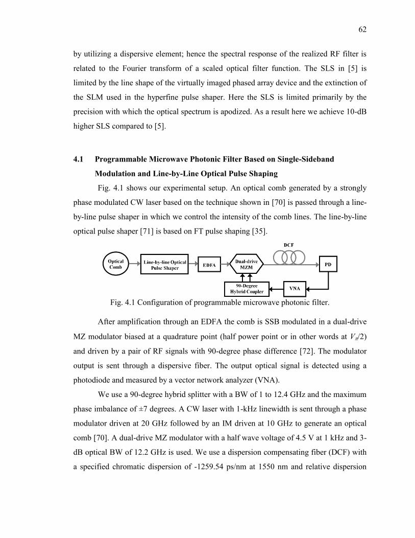
62
by utilizing a dispersive element; hence the spectral response of the realized RF filter is
related to the Fourier transform of a scaled optical filter function. The SLS in [5] is
limited by the line shape of the virtually imaged phased array device and the extinction of
the SLM used in the hyperfine pulse shaper. Here the SLS is limited primarily by the
precision with which the optical spectrum is apodized. As a result here we achieve 10-dB
higher SLS compared to [5].
4.1 Programmable Microwave Photonic Filter Based on Single-Sideband
Modulation and Line-by-Line Optical Pulse Shaping
Fig. 4.1 shows our experimental setup. An optical comb generated by a strongly
phase modulated CW laser based on the technique shown in [70] is passed through a line-
by-line pulse shaper in which we control the intensity of the comb lines. The line-by-line
optical pulse shaper [71] is based on FT pulse shaping [35].
Fig. 4.1 Configuration of programmable microwave photonic filter.
After amplification through an EDFA the comb is SSB modulated in a dual-drive
MZ modulator biased at a quadrature point (half power point or in other words at V/2)
and driven by a pair of RF signals with 90-degree phase difference [72]. The modulator
output is sent through a dispersive fiber. The output optical signal is detected using a
photodiode and measured by a vector network analyzer (VNA).
We use a 90-degree hybrid splitter with a BW of 1 to 12.4 GHz and the maximum
phase imbalance of ±7 degrees. A CW laser with 1-kHz linewidth is sent through a phase
modulator driven at 20 GHz followed by an IM driven at 10 GHz to generate an optical
comb [70]. A dual-drive MZ modulator with a half wave voltage of 4.5 V at 1 kHz and 3-
dB optical BW of 12.2 GHz is used. We use a dispersion compensating fiber (DCF) with
a specified chromatic dispersion of -1259.54 ps/nm at 1550 nm and relative dispersion
63
slope (the ratio of dispersion slope to dispersion at 1550 nm) of 0.00455/nm, resulting in
delay difference of 96 ps between adjacent 10-GHz spaced comb lines (taps). The PD has
a 3-dB BW of 22 GHz with a responsivity of 0.6 A/W. We measure the filter transfer
functions using a VNA over a span of 300 kHz to 20 GHz.
4.1.1 Theoretical model
We assume an optical comb consisting of N lines and write its electric field as
..)(1
0
)(ccepte
N
n
tj
nnn
(4.1)
where pn, n and n are the optical intensity, angular frequency and phase of the n th line
respectively, and c.c. stands for the complex conjugate of the first term on the right side.
For a comb the optical frequencies satisfy n=0+n, and the intensity of the comb
source is periodic at repetition frequency . Later we will see through derivations that
the initial phases of the lines do not affect the RF filter function, which is also verified by
an experiment. The RF electrical signal is split into two equal RF signals with 90 degree
phase difference using a broadband 90-degree hybrid splitter [56]. The RF outputs are
applied to the two arms of the MZ modulator. Each of the comb lines undergoes a SSB
modulation. The output electric field corresponding to the n th line can be written as
..)()sin(
2)cos(
22cceepte
tV
vtjt
V
vtj
nn
RFRF
nnRFRF
nn
(4.2)
where vRF is the voltage amplitude of driving RF signal into the 90-degree hybrid splitter,
and V is the half wave voltage of the MZ modulator. Assuming vRF<<V we can
approximate (4.2) as
..2
)( 4)(cce
V
veepte
tjRFj
tj
nnRFnn
(4.3)
where the first term in the brackets is the output optical carrier and the second term is the
higher frequency sideband generated at n+RF. We note that here we make assumptions
which result in ideal single sideband modulation; however, deviations from these
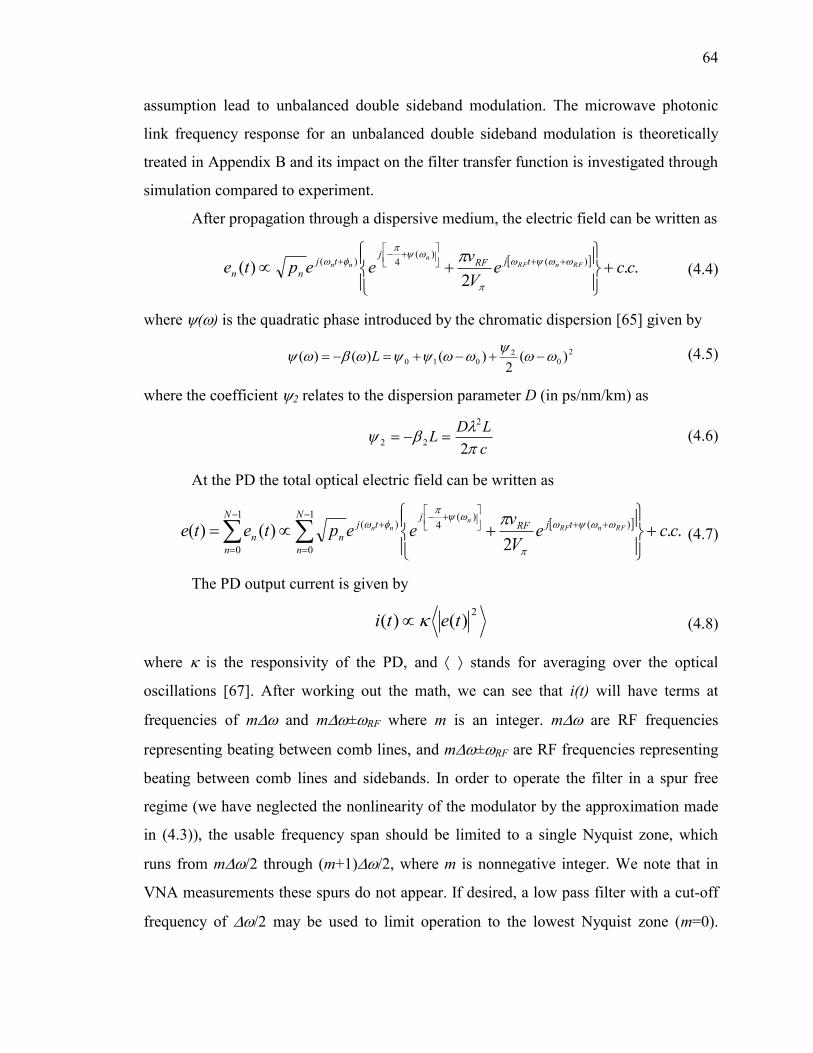
64
assumption lead to unbalanced double sideband modulation. The microwave photonic
link frequency response for an unbalanced double sideband modulation is theoretically
treated in Appendix B and its impact on the filter transfer function is investigated through
simulation compared to experiment.
After propagation through a dispersive medium, the electric field can be written as
..2
)()(
)(4)(
cceV
veepte RFnRF
nnn tjRF
jtj
nn
(4.4)
where () is the quadratic phase introduced by the chromatic dispersion [65] given by
2
02
010 )(2
)()()(
L (4.5)
where the coefficient 2 relates to the dispersion parameter D (in ps/nm/km) as
c
LDL
2
2
22 (4.6)
At the PD the total optical electric field can be written as
..2
)()(1
0
)()(
4)(1
0
cceV
veeptete
N
n
tjRFj
tj
n
N
n
nRFnRF
nnn
(4.7)
The PD output current is given by
2
)()( teti (4.8)
where is the responsivity of the PD, and stands for averaging over the optical
oscillations [67]. After working out the math, we can see that i(t) will have terms at
frequencies of m and m±RF where m is an integer. m are RF frequencies
representing beating between comb lines, and m±RF are RF frequencies representing
beating between comb lines and sidebands. In order to operate the filter in a spur free
regime (we have neglected the nonlinearity of the modulator by the approximation made
in (4.3)), the usable frequency span should be limited to a single Nyquist zone, which
runs from m/2 through (m+1)/2, where m is nonnegative integer. We note that in
VNA measurements these spurs do not appear. If desired, a low pass filter with a cut-off
frequency of /2 may be used to limit operation to the lowest Nyquist zone (m=0).
65
Alternately, a bandpass filter centered at frequency (2m+1)/4 and bandwidth /2 may
be used to limit operation to a single Nyquist zone for m≥1.
After simplification we can show that the component of the current with
frequency RF is given by
..2
)(1
0
)()(cce
V
vpti
N
n
tjRFn
nRFnRF
RF
(4.9)
By substituting in the quadratic phase from (4.5), we find
..2
)(1
0
2
2221
cceV
vpti
N
n
ntjRF
n
RFRFRFRF
RF
(4.10)
Therefore we can write the filter transfer function as
1
0
2 2
221
)(N
n
jn
n
j
RFRF
RFRF
epeH
(4.11)
We notice that the filter spectral amplitude response is periodic in frequency with
a FSR of
T
FSR11
2
(4.12)
where T=2 is the differential delay between taps. By taking an inverse Fourier
transform of (4.11) we can write the time domain impulse response as
1
0
2
)(
2
21
)(N
n
nTtj
nepth
(4.13)
We note that while 2 is negative for a DCF resulting in negative T, -1 is the
total group delay of dispersive fiber and always large enough to guarantee that h(t)
satisfies causality. The impulse response is a scaled version of the comb spectrum, which
is the consequence of frequency-to-time mapping in a dispersive medium. For pn≥0 the
bandpass filter is at m/T where m is an integer. We can shape the filter function by
apodizing the pn’s. From here on we neglect the multiplicative factor preceding the
summation sign in (4.11) since it only has spectral phase.

66
The microwave photonic filters which we implement are based on the concept of
multitap delay line filters that can be modeled by FIR filters. These filters have been fully
studied in digital signal processing as discrete-time FIR filters [73, 74].
4.1.2 Experimental results
In order to compare our experimental results with simulation we make some
assumptions. We run our simulations based on (4.11); however, this relation does not
include some of the factors affecting the overall frequency response of our filter. The
cable loss, the modulator transfer function, and the PD response are all frequency
dependent and roll off for higher frequencies. Since we do not have an accurate measure
of all these frequency responses, therefore we introduce a way to subtract these effects
from experimental results, so that we end up with plots which can be compared with
simulation results. In order to measure the frequency roll-offs, we remove the dispersive
fiber from our setup and connect the output of modulator directly to the PD. Thus we do
not have the filtering response due to tapped delay lines. Then we measure the transfer
function and also record the optical power measured at the PD. Fig. 4.2 shows the filter
transfer function, plotted in RF gain units, when we remove the DCF and the optical
power into the PD is about 5.5 dBm. A thorough derivation of RF gain for the microwave
photonic filters in this chapter is given in Appendix C.
Fig. 4.2 The photonic link frequency response without DCF.
67
Although Fig. 4.2 is measured using the optical comb source, a similar curve is
obtained using the CW laser directly provided that the optical power is held constant.
Most of the roll-off up to ~12 GHz arises from the frequency response of the modulator
which is a well known linear roll-off in logarithmic scale. We also note that 3-dB optical
BW of the modulator translates into 6-dB drop in the RF gain [67]. The measured transfer
function includes all the losses and roll-offs. In comparing our experimental results with
simulation, we subtract this transfer function from our measured filter transfer functions
while correcting for optical power applied to the PD.
Fig. 4.3(a) shows the optical comb at the PD measured using an optical spectrum
analyzer (OSA) when there is no programming applied to the SLM in the line-by-line
pulse shaper. As we notice, the comb is not uniform and the intensity of the lines has
large variation from one to the other. This is a characteristic common to many comb
sources, such as ours, based on strong periodic phase modulation of a CW source.
Fig. 4.3(b) shows the normalized filter transfer function as a solid line and the
simulated filter transfer function as a dashed line. The filter has a 3-dB BW of ~510 MHz
and the main SLS is 9 dB. The location of the bandpass filter gives us the FSR of filter
which is 10.4 GHz, and is in agreement with the 96-ps tap delay. As we see there is a
close agreement between simulated and measured filter functions. The vertical dashed
lines separate the Nyquist zones; the filter can be used in a regime free of sampling spurs
over the span of any one of these zones. This statement also holds for the rest of the
transfer function plots.
Next we apodize the optical comb with a Gaussian apodization using the line-by-
line pulse shaper which is shown in Fig. 4.4(a) measured by an OSA. Due to the Fourier
transform property of the Gaussian function and frequency to time mapping of the
dispersive medium, we expect the filter transfer function also to have a Gaussian profile
in which the sidelobes are highly suppressed. Fig. 4.4(b) shows the normalized filter
transfer function as a solid line and the simulated filter transfer function as a dashed line.
As we see there is a close agreement between simulated and measured filter functions.
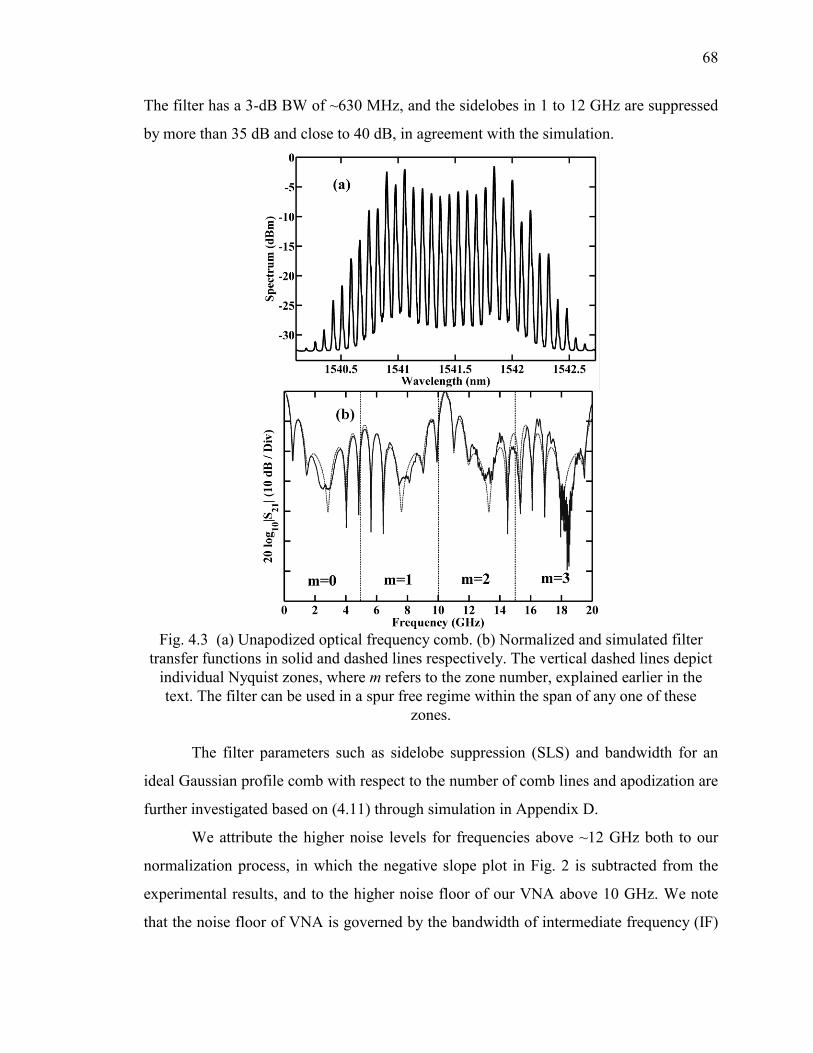
68
The filter has a 3-dB BW of ~630 MHz, and the sidelobes in 1 to 12 GHz are suppressed
by more than 35 dB and close to 40 dB, in agreement with the simulation.
Fig. 4.3 (a) Unapodized optical frequency comb. (b) Normalized and simulated filter
transfer functions in solid and dashed lines respectively. The vertical dashed lines depict
individual Nyquist zones, where m refers to the zone number, explained earlier in the
text. The filter can be used in a spur free regime within the span of any one of these
zones.
The filter parameters such as sidelobe suppression (SLS) and bandwidth for an
ideal Gaussian profile comb with respect to the number of comb lines and apodization are
further investigated based on (4.11) through simulation in Appendix D.
We attribute the higher noise levels for frequencies above ~12 GHz both to our
normalization process, in which the negative slope plot in Fig. 2 is subtracted from the
experimental results, and to the higher noise floor of our VNA above 10 GHz. We note
that the noise floor of VNA is governed by the bandwidth of intermediate frequency (IF)
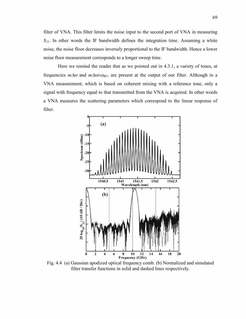
69
filter of VNA. This filter limits the noise input to the second port of VNA in measuring
S21. In other words the IF bandwidth defines the integration time. Assuming a white
noise, the noise floor decreases inversely proportional to the IF bandwidth. Hence a lower
noise floor measurement corresponds to a longer sweep time.
Here we remind the reader that as we pointed out in 4.3.1, a variety of tones, at
frequencies m and m±RF, are present at the output of our filter. Although in a
VNA measurement, which is based on coherent mixing with a reference tone, only a
signal with frequency equal to that transmitted from the VNA is acquired. In other words
a VNA measures the scattering parameters which correspond to the linear response of
filter.
Fig. 4.4 (a) Gaussian apodized optical frequency comb. (b) Normalized and simulated
filter transfer functions in solid and dashed lines respectively.
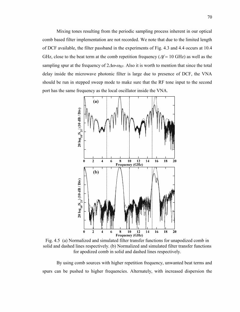
70
Mixing tones resulting from the periodic sampling process inherent in our optical
comb based filter implementation are not recorded. We note that due to the limited length
of DCF available, the filter passband in the experiments of Fig. 4.3 and 4.4 occurs at 10.4
GHz, close to the beat term at the comb repetition frequency (f10 GHz) as well as the
sampling spur at the frequency of 2-RF. Also it is worth to mention that since the total
delay inside the microwave photonic filter is large due to presence of DCF, the VNA
should be run in stepped sweep mode to make sure that the RF tone input to the second
port has the same frequency as the local oscillator inside the VNA.
Fig. 4.5 (a) Normalized and simulated filter transfer functions for unapodized comb in
solid and dashed lines respectively. (b) Normalized and simulated filter transfer functions
for apodized comb in solid and dashed lines respectively.
By using comb sources with higher repetition frequency, unwanted beat terms and
spurs can be pushed to higher frequencies. Alternately, with increased dispersion the
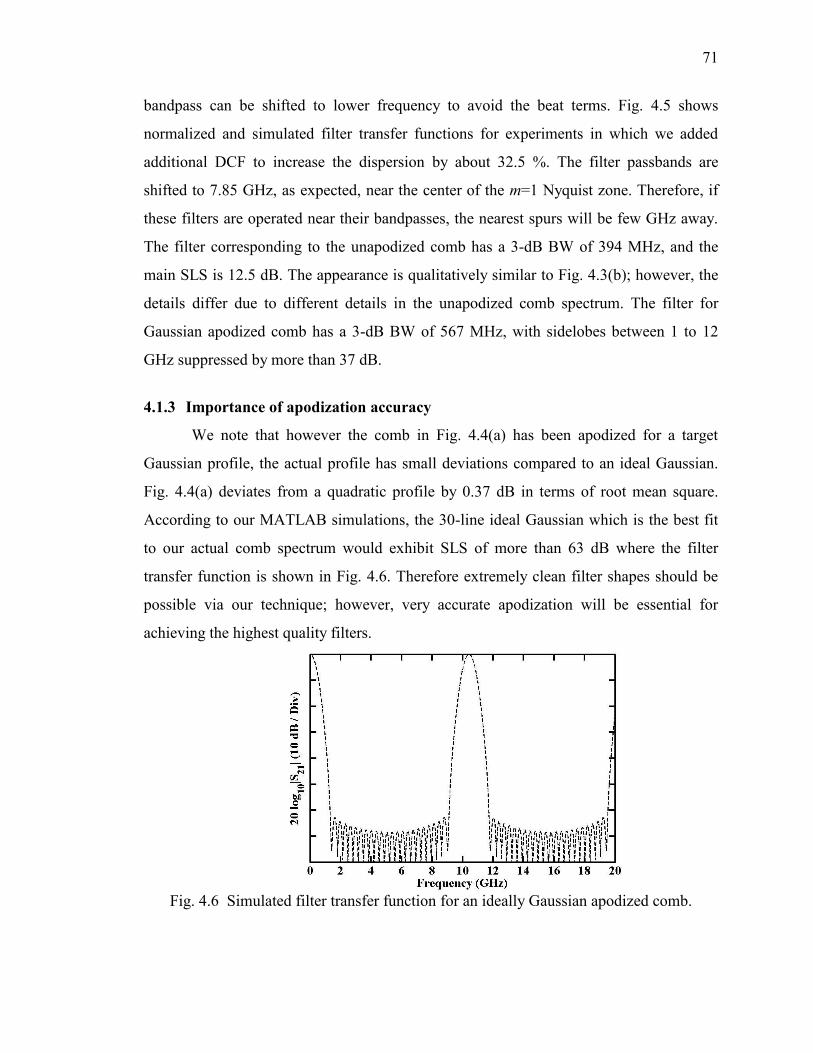
71
bandpass can be shifted to lower frequency to avoid the beat terms. Fig. 4.5 shows
normalized and simulated filter transfer functions for experiments in which we added
additional DCF to increase the dispersion by about 32.5 %. The filter passbands are
shifted to 7.85 GHz, as expected, near the center of the m=1 Nyquist zone. Therefore, if
these filters are operated near their bandpasses, the nearest spurs will be few GHz away.
The filter corresponding to the unapodized comb has a 3-dB BW of 394 MHz, and the
main SLS is 12.5 dB. The appearance is qualitatively similar to Fig. 4.3(b); however, the
details differ due to different details in the unapodized comb spectrum. The filter for
Gaussian apodized comb has a 3-dB BW of 567 MHz, with sidelobes between 1 to 12
GHz suppressed by more than 37 dB.
4.1.3 Importance of apodization accuracy
We note that however the comb in Fig. 4.4(a) has been apodized for a target
Gaussian profile, the actual profile has small deviations compared to an ideal Gaussian.
Fig. 4.4(a) deviates from a quadratic profile by 0.37 dB in terms of root mean square.
According to our MATLAB simulations, the 30-line ideal Gaussian which is the best fit
to our actual comb spectrum would exhibit SLS of more than 63 dB where the filter
transfer function is shown in Fig. 4.6. Therefore extremely clean filter shapes should be
possible via our technique; however, very accurate apodization will be essential for
achieving the highest quality filters.
Fig. 4.6 Simulated filter transfer function for an ideally Gaussian apodized comb.
72
4.1.4 Role of comb lines spectral phase
It is also worth discussing the role of the phase of the optical comb lines out of the
comb generator. Generally, the output of a comb generator such as ours, based on strong
phase modulation of a CW laser, is not a train of bandwidth limited pulses. Although
when desired, we can use the line-by-line pulse shaper to correct the phases of the comb
lines, which does produce a train of bandwidth limited pulses (in other words a phase-
compensated comb). As predicted earlier by (4.11), the spectral phase of the optical comb
source, n, used as the sampling signal does not affect the RF filter response. This
prediction is valid in our experiments conditioned to neglecting the photodiode
nonlinearity for pulsed input. Due to low optical power levels in our experiment the
nonlinearity of photodiode should be minimal even for pulsed input. Further details on
pulsed optical links can be found in [75]. For all experiments we use the uncompensated
comb that its instantaneous optical power varies around its low average power and does
not produce nonlinearity in the photodiode, except in the following experiment for Fig.
4.7(b) where we use the compensated comb.
Instead of the dual-drive MZ modulator depicted in Fig. 4.1, for this experiment
we used a standard MZ IM with a half-wave voltage of 4.75 V at 1 GHz and a 3-dB BW
of 35 GHz. Intensity modulation results in a balanced DSB modulation rather than SSB
modulation. Also for this experiment we employed a SMF with a length of about 70 km
as the dispersive medium. No apodization is employed in these experiments.
Fig. 4.7(a) shows the optical comb measured at the PD. Fig. 4.7(b) shows the
normalized and simulated transfer functions of the filter as solid and dashed lines
respectively when the phases of the comb lines are compensated using the line-by-line
pulse shaper. In this case we verified by intensity autocorrelation measurements that the
comb consisted of a train of pulses, periodic at 10 GHz and with approximately
bandwidth limited pulse durations. This corresponds to at most linear phase across the
comb lines. We note that in this experiment the filter frequency response is affected by
the well-known frequency dependent fading effect due to dispersion acting on both
sidebands; this effect has been included in our simulation [27].

73
Fig. 4.7 (a) Optical frequency comb. (b) Normalized and simulated filter transfer
functions for compensated comb in solid and dashed lines respectively. (c) Normalized
and simulated filter transfer functions for uncompensated comb in solid and dashed lines
respectively.
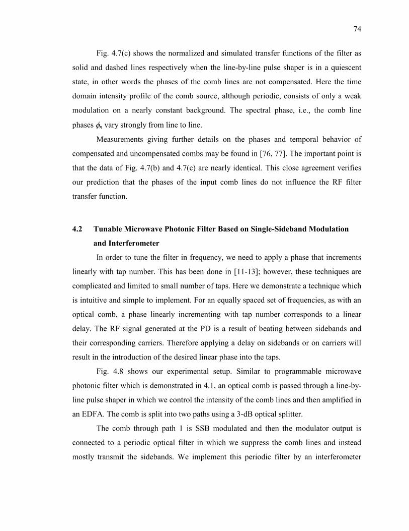
74
Fig. 4.7(c) shows the normalized and simulated transfer functions of the filter as
solid and dashed lines respectively when the line-by-line pulse shaper is in a quiescent
state, in other words the phases of the comb lines are not compensated. Here the time
domain intensity profile of the comb source, although periodic, consists of only a weak
modulation on a nearly constant background. The spectral phase, i.e., the comb line
phases n vary strongly from line to line.
Measurements giving further details on the phases and temporal behavior of
compensated and uncompensated combs may be found in [76, 77]. The important point is
that the data of Fig. 4.7(b) and 4.7(c) are nearly identical. This close agreement verifies
our prediction that the phases of the input comb lines do not influence the RF filter
transfer function.
4.2 Tunable Microwave Photonic Filter Based on Single-Sideband Modulation
and Interferometer
In order to tune the filter in frequency, we need to apply a phase that increments
linearly with tap number. This has been done in [11-13]; however, these techniques are
complicated and limited to small number of taps. Here we demonstrate a technique which
is intuitive and simple to implement. For an equally spaced set of frequencies, as with an
optical comb, a phase linearly incrementing with tap number corresponds to a linear
delay. The RF signal generated at the PD is a result of beating between sidebands and
their corresponding carriers. Therefore applying a delay on sidebands or on carriers will
result in the introduction of the desired linear phase into the taps.
Fig. 4.8 shows our experimental setup. Similar to programmable microwave
photonic filter which is demonstrated in 4.1, an optical comb is passed through a line-by-
line pulse shaper in which we control the intensity of the comb lines and then amplified in
an EDFA. The comb is split into two paths using a 3-dB optical splitter.
The comb through path 1 is SSB modulated and then the modulator output is
connected to a periodic optical filter in which we suppress the comb lines and instead
mostly transmit the sidebands. We implement this periodic filter by an interferometer
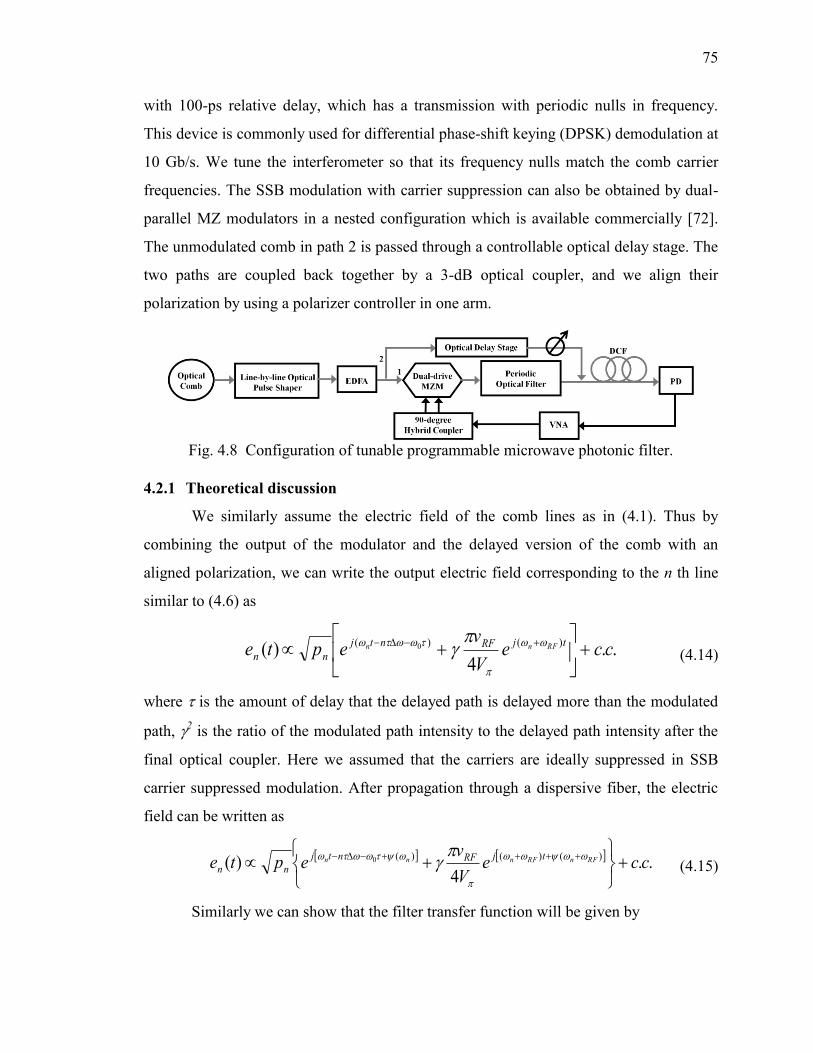
75
with 100-ps relative delay, which has a transmission with periodic nulls in frequency.
This device is commonly used for differential phase-shift keying (DPSK) demodulation at
10 Gb/s. We tune the interferometer so that its frequency nulls match the comb carrier
frequencies. The SSB modulation with carrier suppression can also be obtained by dual-
parallel MZ modulators in a nested configuration which is available commercially [72].
The unmodulated comb in path 2 is passed through a controllable optical delay stage. The
two paths are coupled back together by a 3-dB optical coupler, and we align their
polarization by using a polarizer controller in one arm.
Fig. 4.8 Configuration of tunable programmable microwave photonic filter.
4.2.1 Theoretical discussion
We similarly assume the electric field of the comb lines as in (4.1). Thus by
combining the output of the modulator and the delayed version of the comb with an
aligned polarization, we can write the output electric field corresponding to the n th line
similar to (4.6) as
..4
)()()( 0 cce
V
vepte
tjRFntj
nnRFnn
(4.14)
where is the amount of delay that the delayed path is delayed more than the modulated
path, 2 is the ratio of the modulated path intensity to the delayed path intensity after the
final optical coupler. Here we assumed that the carriers are ideally suppressed in SSB
carrier suppressed modulation. After propagation through a dispersive fiber, the electric
field can be written as
..4
)()()()(0 cce
V
vepte RFnRFnnn tjRFntj
nn
(4.15)
Similarly we can show that the filter transfer function will be given by
76
1
0
)(2 2
2210
)(N
n
jn
n
j
RFRF
RFRF
epeH
(4.16)
The most important point is that the transfer function can be tuned in the
frequency domain by controlling the relative delay between two paths. The RF
frequency shift is given by
22
f (4.17)
Therefore a programmable tuning can be achieved by a programmable optical
delay stage. We also note although the optical phase shift referenced to the carrier
frequency is transferred directly into the RF domain, it doesn’t affect tuning of the
filter. That is, the spectral amplitude response of the filter in (4.16) is independent of this
phase.
From a practical point of view, obtaining a SSB carrier suppressed modulation is a
difficult task. Errors in fabrication of dual-parallel MZ modulators, imbalance of RF
signals’ strength, and imbalance of 90-degree hybrid splitter result in non-ideal operation
and presence of residual carrier after modulation. Also the thermal drift and sensitivity to
biasing voltages lead us to a controlling circuitry with a feedback loop for biasing the
modulator. Here we briefly explain what will happen in the presence of residual carrier.
The beat between the sidebands from the modulated path and the carriers through the
delayed path will result in a tunable filter as (4.16), but also the beat between the
sidebands and the carriers through the modulated path results in a non-tunable filter
which is given by (4.11). By neglecting the common multiplicative spectral phase factor
preceding the summation sign in (4.11) and (4.16), we can write the overall filter
frequency response as
1
0
)(1
0
202)(N
n
jn
n
jN
n
jn
nRFRFRF epeepH
(4.17)
We point out a few assumptions that we have made in our analysis above. First,
we have assumed the coherence time of individual optical comb lines is large compared
to the small delay between modulated and delayed paths. This is easily satisfied for

77
practical comb sources. Note however that spectral sliced ASE sources, used in [10] for
example, do not meet this coherence time criterion and cannot be employed in our
scheme. Also we assume that the polarizations are aligned and that there are negligible
polarization rotation fluctuations. Finally, note that when the intensity in the modulated
path is much less than the intensity in the delayed path, in other words for small values of
, we can ignore the first term on the right side of (4.17), and it will be simplified to
(4.16).
Here we briefly explain what coupling ratio should be chosen for the optical
splitter and coupler in our scheme. For the given optical power input to the splitter, we
can show that the desired RF signal with a frequency of RF (or in other words the filter
transfer function) generated at the PD is also proportional to
)1()1()( RFH (4.18)
where and are the splitter and coupler coupling coefficients in terms of power. As we
can see the above expression is maximized when and are chosen equal to 0.5, or in
other words we choose 3-dB splitter and couplers.
We note that the DPSK demodulator interferometer which we use for carrier
suppression also alters the frequency response of our implemented filters; however, this
change is irrelevant when a SSB carrier suppressed modulation is used. The filter transfer
function in presence of DPSK demodulator interferometer is given by
1
0
)(1
0
202)1(2
cos)1()(N
n
jn
n
jN
n
jn
nRF
RFRFRF epeepH
(4.19)
where is the ratio of the nulls’ amplitude to the peaks’ amplitude of demodulator
interferometer in terms of power transmission, or in other words -10log10 (dB) is the
degree of extinction with which the demodulator interferometer suppress the carriers.
Here we assumed 3-dB splitter and coupler. For small values of the first term in
brackets on the right side vanishes and (4.19) will simplify as
1
0
)( 20 sin)(N
n
jn
nRFj
RFRFepeH
(4.20)
78
4.2.2 Experimental results
Now in order to demonstrate filter tunability, we configure our setup as in Fig.
4.8. As we discussed earlier we use 3-dB splitter and coupler to obtain the minimum loss.
To measure the Gaussian apodized optical comb at the PD, shown in Fig. 4.9(a), we
disconnect the modulator path. The normalized filter transfer function is plotted in Fig.
4.9(b) in solid line. The filter passband occurs at 2.1 GHz which corresponds to a relative
delay of m.100-20 ps, where m is an integer. We use (4.20) to simulate the filter transfer
function which is shown in Fig. 4.9(b) in dashed line.
In order to show tuning we reduce the delay in the delayed path by 30 ps and we
measure the transfer function. We expect the bandpass filter shifts by 3.12 GHz to higher
frequency. Fig. 4.9(c) shows the normalized and simulated transfer functions in solid and
dashed lines respectively where the passband occurs at 5.25 GHz. The frequency shift is
very much as expected given the change in relative delay. The filter of Fig. 4.9(c) has a 3-
dB BW of ~720 MHz and 36-dB SLS over 0-10 GHz. These results confirm our
prediction that filter tuning is possible, without baseband response and without significant
change in passband width, by varying delay in an interferometric setup.
Compared to Fig. 4.4, Fig. 4.9 shows higher noise and some spurious peaks which
we discuss briefly in the following. First, we believe that the spurious peaks around 8.5
and 11.4 GHz in Fig. 4.9 (b) and (c) respectively arise due to undesired reflection in our
setup. In effect this could lead to an unwanted weak interference component with a
different delay, corresponding to a different passband frequency. Therefore, for future
experiments care should be taken to reduce reflections, possibly taking advantage of
optical isolators. On the other hand the degradation of the 90-degree hybrid splitter above
12.4 GHz, not included in our simulations, results in unbalanced DSB modulation which
can also produce undesired filter responses for frequencies above 12.4 GHz, to which we
attribute the spurious peak at 18.7 GHz in Fig. 4.9(b). Finally we attribute the very weak
peaks at 10.4 GHz in Fig. 4.9 (b) and (c), which are more than 40-dB down compared to
passband peak at 5.25 GHz in Fig. 4.9(c), to finite extinction of the carrier in the
modulator path.
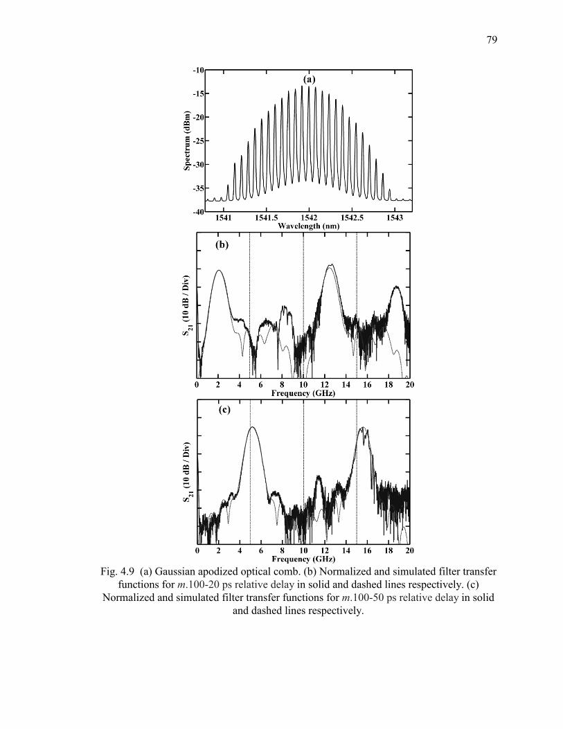
79
Fig. 4.9 (a) Gaussian apodized optical comb. (b) Normalized and simulated filter transfer
functions for m.100-20 ps relative delay in solid and dashed lines respectively. (c)
Normalized and simulated filter transfer functions for m.100-50 ps relative delay in solid
and dashed lines respectively.
80
As in Fig. 4.8(b), any remaining carrier is expected to contribute a peak at the
filter FSR, 10.4 GHz. We also notice from (4.20) that the use of a filter for carrier
suppression in our tuning experiments of Fig. 4.9 leads to a sin(RF/) frequency
dependent attenuation factor that is not present for the data of Fig. 4.4; this effect has
been taken into account in our simulation.
Also as predicted in (4.18), for fixed input optical power, the interferometric filter
configuration provides lower RF gain compared to the single path (noninterferometric)
configuration. For 3-dB splitter and coupler the theoretical RF gain decreases by 12 dB.
Hence, we expect that our bandpass filter tuned to 5 GHz has a 12-dB lower RF gain
compared to Fig. 4.4(b). The bandpass filter at 5.25 GHz in Fig. 4.9(c) has 15-dB higher
loss which agrees closely since the DPSK demodulator interferometer has an additional
insertion loss of about 2 dB. In the future it should be possible to restore some of the
reduced RF gain by using a complementary modulator configuration with differential
detection [78].
Finally we scan the delay stage in increments of 0.9375 mm (round trip delay of
6.25 ps) and measure the filter transfer function. The center of filter’s passband as a
function of the relative delay is plotted in Fig. 4.10. The solid circles show the measured
filter’s passband center and the solid line shows a linear fit to the experimental results.
The fit has a slope of 0.1025 GHz/ps.
Fig. 4.10 Tunable filter passband center vs. relative delay .

81
This corresponds to 10.25-GHz frequency shift for a relative delay of 100 ps,
which introduces a 2-incremental phase shift between adjacent taps; this closely agrees
with the measured FSR of 10.4 GHz. The maximum deviation of the linear fit from the
experimental results is 117 MHz. This clearly confirms the linear frequency tuning with
respect to the programmable delay predicted by (4.17).
4.3 Tunable Microwave Photonic Filter Based on Single-Sideband Modulation,
Phase-Programming Optical Pulse Shaper and Interferometer
As we discussed in previous part the linearly incrementing phase introduced into
taps can be done by relatively delaying one of the arms in our interferometric scheme.
Although the line-by-line pulse shaping setup which is used to apodize the comb lines
intensities can also be utilized to impose an arbitrary phase onto comb lines. Therefore a
multitap microwave photonic filter with complex tap coefficients can be realized. Here for
the proof of concept we apply an evenly increasing or decreasing phase across comb lines
that corresponds to a programmable delay and we can tune the bandpass filter location.
Fig. 4.11 shows our experimental setup which is similar to Fig. 4.8 except that the
pulse shaper is relocated to after the modulator. We have removed the DPSK demodulator
to avoid higher loss in modulated path but the splitter and coupler coupling coefficients
and the losses in modulator and the line-by-line pulse shaper are such that the carriers at
the end of path 1 are about 20-dB weaker than the carriers in path 2.
Fig. 4.11 Configuration of multitap microwave photonic filter with complex coefficient
taps.
Similar to (4.17) we can write the filter transfer function as
1
0
)(1
0
202)(N
n
jjn
n
jN
n
jn
nRFnRFRF epeepH (4.21)

82
where n are the phase applied by the line-by-line pulse shaper, and is the relative delay
between two path. For small (here equals to -20 dB) we can neglect the first term on the
right side of equation and we will have
1
0
)( 2)(N
n
jjn
nRFnRFepH (4.22)
As we notice in (4.22) there are two mechanisms which can tune the bandpass
filter location; controlling the relative optical delay between two paths or introducing
linear spectral phase across comb lines. In order to measure the comb at the PD which is
shown in Fig. 4.12(a) the path 1 was disconnected.
Fig. 4.12 (a) Unapodized optical frequency comb. (b) Normalized and simulated
filter transfer functions in solid and dashed lines respectively.
83
Fig. 4.12(b) shows the filter transfer function measured using VNA in solid line
when the pulse shaper is quiescent. Here also in order to account for the modulator roll-
off we normalize the measured transfer function by the transfer function in the absence of
DCF similar to 4.3.2. We note that the filter passband is located at 3.3 GHz which
corresponds to relative delay of 31.7 ps since we assume zero phase is applied to the
comb lines. We calculate the filter transfer function using (4.22) which is plotted as a
dashed line in Fig. 4.12(b).
Now we apply a linearly decreasing phase in steps of /8 to the comb lines by
programming the line-by-line pulse shaper. The normalized measured filter transfer
function is shown in Fig. 4.13(a). As we expect the filter passband shifts to higher
frequencies by 0.7 GHz which is in close agreement with the theoretical value of FSR/16
= 0.65 GHz.
Fig. 4.13 The normalized measured filter transfer functions for a linearly increasing
phase in steps of -/8, /8, /4 and /2 in (a), (b), (c) and (d) respectively.

84
The normalized measured filter transfer functions for a linearly increasing phase
in steps of /8, /4 and /2 are shown in Fig. 4.13 (b), (c), (d) respectively, and the filter’s
passbands occur at 2.68, 2 and 0.77 GHz. We note that the filter passband location can be
tuned by programming the line-by-line pulse shaper as a linear spectral phase filter which
corresponds to a programmable delay in path 1. From practical point of view it is
advantageous to embed the pulse shaper into path 2 since the spatial location of comb
lines with respect to SLM pixels is fixed; however, the spatial location of sidebands also
depends on radio frequency which can degrade the performance of the filter due to finite
resolution of the pulse shaper. We also note that the tap intensities still can be apodized
by programming the transmission of the pulse shaper since tap intensity is a product of
carrier electric field in path 2 and the sideband electric field in path 1.
This scheme enables to arbitrarily program the taps’ phase and amplitude. In other
words, a user defined FIR multitap filter with complex coefficients can be implemented
through this scheme.
4.4 Tunable Microwave Photonic Filter Based on Intensity Modulation and
Interferometer
To achieve SSB modulation a dual-drive modulator and a 90-degree hybrid are
necessary. In Fig. 4.11 we also utilize a two-arm 100-ps interferometer (DPSK
demodulator) to suppress the optical carriers. In order to eliminate extra component and
cost while significantly reducing the electrical complexity we introduce a new scheme
which is based on an IM biased at its minimum transmission resulting in balanced DSB
modulation with carrier suppression. Coherent detection in an RF photonic link with a
single CW input laser based on an IM biased at its minimum transmission has been
already investigated in [79].
Fig. 4.14 shows our experimental setup similar to Fig. 4.11 where we replace
dual-drive modulator and hybrid with an IM. We note that this scheme which is similar to
[6] enables controlling individual taps using the line-by-line pulse shaping while in

85
contrast it doesn’t suffer from residual passband response and it is simpler since it doesn’t
require a custom designed double input MZ modulator.
Again we assume the electric field of the comb lines given by (4.1). Assuming a
chirp free modulator the output electric field corresponding to the n th line can be written
as
..)()sin(
cceeptet
V
vtj
tj
nn
RFRF
n
n
(4.23)
Thus by combining the output of the modulator and the delayed version of the
comb with an aligned polarization, we can write the total electric field corresponding to
the n th line in the first order approximation as
..)sin(2
)()( 0 cct
V
vjeepte RF
RFnjtj
nnn
(4.24)
where is the amount of delay that path 2 is delayed more than path 1. Here we assumed
that the carriers are ideally suppressed in DSB carrier suppressed modulation. After
simplification we can show that the component of the current with frequency RF is given
by
..
2)(
022
2
022
2
2
1
0
2
cce
eV
vpti
RFRFRF
RFRFRF
RF
nntj
N
n
nntjRF
n
(4.25)
Therefore we can write the filter transfer function as
1
0
)(21
0
)(2 20
22
20
22
)(N
n
jn
n
jN
n
jn
n
j
RFRF
RFRF
RF
epeepeH
(4.26)
The two terms on the right in (4.26) are the transfer functions of two filters with
an identical spectral amplitude response periodic in frequency with a FSR of

86
T
FSR11
2
(4.27)
The first and second filters are shifted respectively to higher and lower
frequencies with respect to baseband and its replicas at integer FSRs by the amount
22
f (4.28)
We note that photonic links with DSB modulation and dispersive fiber show
fading at certain frequencies [80]. Although in our interferometric configuration the two
terms that normally destructively interfere are now split into two different frequency
passbands, and fading no longer occurs.
A CW laser with specified 1-kHz linewidth is sent through a phase modulator
driven at 10 GHz followed by an IM driven at 10 GHz to generate an optical comb. An
MZ IM with a half-wave voltage of 4.75 V at 1 GHz and 3-dB optical BW of 35 GHz is
used. We use a DCF with a specified chromatic dispersion of -1259.54 ps/nm at 1550 nm
and relative dispersion slope (the ratio of dispersion slope to dispersion at 1550 nm) of
0.00455/nm, resulting in delay difference of 96 ps between adjacent 10-GHz spaced comb
lines (taps). The PD has a 3 dB BW of 22 GHz with a responsivity of 0.6 A/W. We
measure the filter transfer functions using a VNA over a span of 300 kHz-20 GHz.
Fig. 4.14 Configuration of microwave photonic filter based on IM biased at minimum
transmission.
Fig. 4.15(a) shows the optical comb at the PD generated using the scheme in [81]
when there is no programming applied to the SLM in the line-by-line pulse shaper. As we
notice, although the comb is relatively flat, the intensity of the lines has some variation
87
from one to the other. This is a characteristic common to many comb sources, such as
ours, based on strong periodic phase modulation of a CW source.
Fig. 4.15(b) shows the measured filter transfer function in solid line and the
simulated filter transfer function in dashed line. The filter has a 3-dB BW of ~245 MHz
and the main SLS is 16.5 dB. The first filter passband occurs at 2.98 GHz which
corresponds to a relative delay of m.100+29 ps, where m is an integer. The second
bandpass occurs at FSR-2.98 GHz as predicted by our analysis. The spacing between first
and third filter passbands gives us the FSR of filter which is 10.4 GHz. As we see there is
a close agreement between simulated and measured filter functions.
Fig. 4.15 (a) Unapodized optical frequency comb. (b) Measured and simulated filter
transfer functions in solid and dashed lines respectively.
Next we apodize the optical comb with a Gaussian apodization which is shown in
Fig. 4.16(a) using the line-by-line pulse shaper. To measure the Gaussian apodized
optical comb at the PD we disconnect the modulator path.
88
Due to the Fourier transform property of Gaussian function, we expect the filter
transfer function also to have a Gaussian profile in which the sidelobes are highly
suppressed. Fig. 4.16(b) shows the measured filter transfer function in solid line and the
simulated filter transfer function in dashed line. As we see there is a close agreement
between simulated and measured filter functions. The filter has a 3-dB BW of ~340 MHz,
and the sidelobes between 0 to 10 GHz are suppressed by more than 26 dB and mostly by
32 dB, in agreement with the simulation.
Fig. 4.16 (a) Gaussian apodized optical frequency comb. (b) (c) (d) Measured and
simulated filter transfer functions for relative delays of m.100+29 ps, m.100+10 ps and
m.100+48 ps in solid and dashed lines respectively.
We note that although the comb in Fig. 4.16(a) has been apodized for a target
Gaussian profile, the actual profile has some deviations compared to an ideal Gaussian.
Fig. 4.16(a) deviates from a quadratic profile by 0.47 dB in terms of root mean square.
According to our MATLAB simulations, the 56-line ideal Gaussian which is the best fit
to our actual comb spectrum would exhibit SLS of more than 72 dB. Therefore extremely
89
clean filter shapes are potentially possible via our technique, although very accurate
apodization will be essential for achieving the highest quality filters.
Now in order to demonstrate filter tunability, we control the delayed path. The
measured filter transfer function is plotted in Fig. 4.16(c) in solid line. The bandpass filter
occurs at 1.02 GHz which corresponds to a relative delay of m.100+10 ps, where m is an
integer. The sidelobes are suppressed by more than 31 dB. We use (4.26) to simulate the
filter transfer function which is shown in Fig. 4.16(c) in dashed line. In order to show
tuning we increase the delay in the delayed path by 38 ps and we measure the transfer
function. We expect the first filter passband in Fig. 4.16(c) to shift by 4 GHz to higher
frequency. Fig. 4.16(d) shows the measured and simulated transfer functions in solid and
dashed lines respectively where the first and second bandpasses occur at 4.99 and 5.4
GHz respectively. The frequency shift is very much as expected given the change in
relative delay. Now in this limiting case the two transfer functions in (4.26) partially
overlap resulting in a wider bandpass filter. The filter of Fig. 4.16(d) has a 3-dB BW of
~820 MHz and 27-dB SLS.
90
5. SUMMARY AND FUTURE PROSPECT
In the past few years, many techniques have been developed for photonic
generation of electrical signals, which later on received great attention due to growing
radio-over-fiber (RoF) technology. This has been in response to the growing need for
higher data rates in communication systems which result in large bandwidth signals. The
primary limiting factor in handling these large bandwidth signals has been the generating
and processing interfaces of wireless transmitters and receivers. Although these large
bandwidth electrical signals have been realized through photonic techniques and
developing electronic techniques, technology for fast processing and filtering of these
signals is still missing. Therefore we have investigated photonic techniques for
processing of ultra-broadband RF waveforms at receiving front end. These techniques can
find wide spread use in many ultra-broadband communication settings.
Essentially the photonic processing techniques investigated in our research can be
modeled as an RF photonic link which has been studied for many years [82]. One of the
important parameters of an RF photonic link is noise figure which is a function of
insertion loss, laser induced noise and photodetector thermal noise. The insertion loss
which is currently considerable in our demonstrated techniques dominates the noise
figure leading to the degradation of SNR. The insertion loss of an RF photonic link is
governed by few factors; the half wave voltage of the MZ modulator, the optical source
power, the optical insertion loss of the optical elements such as optical pulse shaper and
dispersive fiber, and the responsivity of the photodetector. Recent efforts have led to
modulators with half-wave voltage less than 1 V [83] which results in much lower RF
photonic link loss. The optical source power can be increased to obtain a lower loss RF
photonic link or even turn an RF photonic link into an amplifier [84]; however, this is
91
ultimately limited by the power handling of the optical components and more importantly
the photodetector. Although the implementation of free space optical pulse shapers with
lower insertion loss is theoretically possible, the integration of optical pulse shapers can
significantly decrease their insertion loss and improve their robustness while greatly
reducing their size [85]. Utilization of very low loss DCF or fiber Bragg grating can
provide large amount of dispersion while having low loss which can even further reduce
the RF photonic loss of our microwave photonic filters demonstrated in chapter four.
Finally large bandwidth photodetectors with higher power handling and higher efficiency
can decrease the RF photonic link loss [86].
Recently there has been a lot of ongoing research in the integration of photonics
onto chip level devices. This was initiated by optical interconnects to enable the transfer
of high data rates between processors in next generation computers [87]. In order to be
compatible with electronic technology the photonic device research for interconnect
applications has been mainly focused on silicon technology which is referred as silicon
photonics [88]. Silicon photonics has been a promising technology to integrate photonic
devices such as lasers, modulators, couplers, splitters, multiplexers, demultiplexers,
switches, delay lines, dispersive waveguides, resonators, array waveguide gratings,
photodetectors, etc. [89-95] into low loss, small size, high reliability, and low cost on-
chip devices. Although all these devices has not been yet fabricated on a single chip to
implement an on-chip optical interconnect, they provide the building blocks of our
demonstrated photonic processing techniques that can potentially enable full integration
of these techniques into silicon photonics. We note that micro ring resonators integrated
into silicon photonics has been already utilized to demonstrate photonically assisted RF
arbitrary waveform generation [22] and microwave photonic notch filter [96].
Finally the dynamic range of our proposed techniques also follows the dynamic
range of an RF photonic link which is mainly governed by the nonlinearity of MZ
modulator and photodiode. The linearity of RF photonic links has been well investigated
and there is still ongoing research in this field [97]. Other forms of RF photonic links
with different modulation formats and detection schemes may be adopted in order to
92
improve the dynamic range and the noise figure in our proposed photonic processing
techniques [98].
5.1 Fast Real-Time Ultra-Broadband RF Waveform Identification
We demonstrated ultra-broadband RF photonic matched filters for the
compression of arbitrary RF waveforms with time apertures larger than 700 ps, in excess
of 15-GHz spectral content and almost 200% fractional bandwidth. It is worth noting that
the longest waveform time apertures which this filter can process is limited by the
spectral resolution of hyperfine optical pulse shaper, and the shortest time domain
features is defined by the filter total bandwidth. In other words the complexity of the
waveforms is given by their time-bandwidth product corresponding to the filter time-
bandwidth product. A 2-D optical pulse shaper can process high complexity waveforms
however for the price of a much larger bandwidth [99]. Since RF systems have ultimate
limitations on their bandwidth, to be able to process high complexity RF waveforms
using this filter a hyperfine optical pulse shaper with a narrower spectral resolution is
necessary. As an application example the compression of chirp waveform technique
which we demonstrated in chapter two can be utilized to implement the scheme proposed
in [100] for multi-access communication system.
5.2 Toward Dispersion Free Wireless Communication Systems
Although low dispersion antennas are available, but depending on directivity,
size, etc. in a wireless link, antennas may be utilized which induce nonlinear spectral
phase resulting in distortion of received signal while other RF components in the
transmitter and receiver may also contribute a nonlinear spectral phase into the signal.
Therefore programmable spectral phase filters which can overcome dispersion are
practically appealing. The dispersion arising from antennas becomes more pronounced in
the transmission of broadband RF signals. We note that this scheme still doesn’t
compensate the dispersion arising from multipath which results in channel spectral
amplitude variations.
93
In chapter three we introduced the application of microwave photonic phase filters
to post-compensate broadband antenna dispersion. We showed how the distorted impulse
response of a wireless link in LOS can be restored to its bandwidth limit duration in an
ultra-broadband regime. We further demonstrated how this technique can be utilized in
radar systems to approach their ultimate bandwidth limit resolution in time domain while
benefiting from being real time and asynchronous which can significantly improve the
processing speed [54]. We also investigated that dispersion compensation combined with
matched filtering at the receiver may be employed for identification of user defined
waveforms in wireless system.
Since these microwave photonic filters are essentially based on matched filters
introduced in chapter two, all the possible improvements mentioned earlier are also
applicable here. In addition the time aperture of impulse response of dispersive antennas
is commonly large; hence a microwave photonic phase filter with large time aperture is
desirable. Due to time-bandwidth product relation, this translates into very high spectral
resolution in hyperfine optical pulse shapers.
5.3 Microwave Photonic Filter with Large Number of Complex Coefficient Taps
We presented the application of optical comb sources in multitap microwave
photonic filters to increase the number of available taps in these filters. We utilized line-
by-line optical pulse shaping as a tool to control the intensity of comb lines which results
in individually programming of taps’ amplitudes. We demonstrated an interferometric
scheme to introduce an incremental linear phase into taps by a programmable optical
delay to tune the location of bandpass filter. By embedding the line-by-line optical pulse
shaper into one arm of the interferometer the phase introduced onto each tap can be also
programmed. Therefore we can implement a microwave photonic filter with arbitrary
complex tap weights which can be used to design variety of filters. The large number of
taps and apodization of comb profile enables us to implement highly selective
programmable filters with high sidelobe suppression and sharpness while complex tap
weights lead us to tunable and more versatile filters.
94
On the other hand the development of optical frequency combs with higher
repetition rates can increase the usable bandwidth of these filters while higher number of
comb lines enables more freedom in shaping the bandpass filter. Generation of optical
combs which inherently possess the desirable apodizations eliminates the need for optical
pulse shaping [81].
As we noted in chapter four these filters suffer from intermodulation distortion.
This issue invokes for further investigation and research to find techniques which
eliminate or minimize this undesirable effect [101, 102].
These filters can be used in ultra-broadband RF systems for filtering where fast
reconfiguration and tuning are required. Since these filters retain arbitrary FIR, they can
be utilized in fast processing of analog signals as a counter part of discrete time signal
processing techniques. A large range of sampling windows and their corresponding
transfer functions are given in [103] which can be implemented using our scheme. These
filters can be also used as a part of a RAKE receiver in a multipath environment to
enhance the performance of RF communication systems [104].

LIST OF REFERENCES
95
LIST OF REFERENCES
[1] K. Wilner, and A. P. Van Den Heuvel, “Fiber-optic delay lines for microwave signal
processing,” Proc. IEEE, vol. 64, no. 5, pp. 805-807, May 1976.
[2] J. P. Yao, “Microwave photonics,” J. Lightw. Technol., vol. 27, no. 3, pp. 314-335,
Feb. 2009.
[3] W. Ng, A. A. Walston, G. L. Tangonan, J. J. Lee, I. L. Newberg, N. Bernstein, “The
first demonstration of an optically steered microwave phased array antenna using
true-time-delay,” J. Lightw.Technol., vol. 9, no. 9, pp. 1124-1131, Sep. 1991.
[4] A. Ortigosa-Blanch, J. Mora, J. Capmany, B. Ortega, and D. Pastor, “Tunable radio-
frequency photonic filter based on an actively mode-locked fiber laser,” Opt. Lett.,
vol. 31, no. 6, pp. 709-711, Mar. 2006.
[5] S. Xiao, and A. M. Weiner, “Coherent photonic processing of microwave signals
using spatial light modulator: programmable amplitude filters,” J. Lightw. Technol.,
vol. 24, no. 7, pp. 2523-2529, Jul. 2006.
[6] J. Mora, A. Ortigosa-Blanch, D. Pastor, and J. Capmany, “Tunable microwave
photonic filter free from baseband and carrier suppression effect not requiring single
sideband modulation using a Mach-Zenhder configuration,” Opt. Exp., vol. 14, no.
17, pp. 7960-7965, Aug. 2006.
[7] A. Loayssa, J. Capmany, M. Sagues, and J. Mora, “Demonstration of incoherent
microwave photonic filters with all-optical complex coefficients,” IEEE Photon.
Technol. Lett., vol. 18, no. 16, pp. 1744-1746, Aug. 2006.
[8] J. Mora, S. Sales, M. D. Manzanedo, R. Garcia-Olcina, J. Capmany, B. Ortega, and
D. Pastor, “Continuous tuning of photonic transversal filter based on the
modification of tapped weights,” IEEE Photon. Technol. Lett., vol. 18, no. 15, pp.
1594-1596, Aug. 2006.
[9] S. Xiao, and A. M. Weiner, “Programmable photonic microwave filters with
arbitrary ultra-wideband phase response,” IEEE Trans. Microw. Theory Tech., vol.
54, no. 11, pp. 4002-4008, Nov. 2006.
[10] J. H. Lee, Y. M. Chang, Y. G. Han, S. B. Lee, and H. Y. Chung, “Fully
reconfigurable photonic microwave transversal filter based on digital micromirror
device and continuous-wave, incoherent supercontinuum source,” Appl. Opt., vol.
46, no. 22, pp. 5158-5167, Aug. 2007.
[11] M. Sagues, A. Loayssa, and J. Capmany, “Multitap complex-coefficient incoherent
microwave photonic filters based on stimulated Brillouin scattering,” IEEE Photon.
Technol. Lett., vol. 19, no. 16, pp. 1194-1196, Aug. 2007.
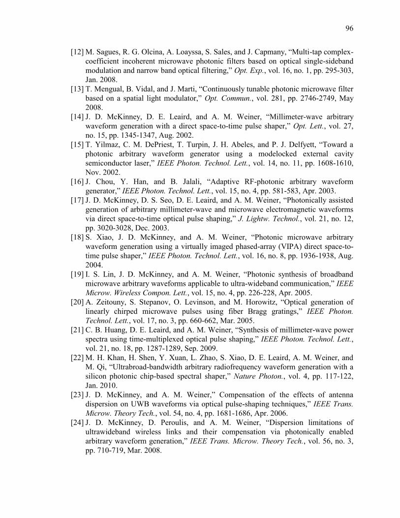
96
[12] M. Sagues, R. G. Olcina, A. Loayssa, S. Sales, and J. Capmany, “Multi-tap complex-
coefficient incoherent microwave photonic filters based on optical single-sideband
modulation and narrow band optical filtering,” Opt. Exp., vol. 16, no. 1, pp. 295-303,
Jan. 2008.
[13] T. Mengual, B. Vidal, and J. Marti, “Continuously tunable photonic microwave filter
based on a spatial light modulator,” Opt. Commun., vol. 281, pp. 2746-2749, May
2008.
[14] J. D. McKinney, D. E. Leaird, and A. M. Weiner, “Millimeter-wave arbitrary
waveform generation with a direct space-to-time pulse shaper,” Opt. Lett., vol. 27,
no. 15, pp. 1345-1347, Aug. 2002.
[15] T. Yilmaz, C. M. DePriest, T. Turpin, J. H. Abeles, and P. J. Delfyett, “Toward a
photonic arbitrary waveform generator using a modelocked external cavity
semiconductor laser,” IEEE Photon. Technol. Lett., vol. 14, no. 11, pp. 1608-1610,
Nov. 2002.
[16] J. Chou, Y. Han, and B. Jalali, “Adaptive RF-photonic arbitrary waveform
generator,” IEEE Photon. Technol. Lett., vol. 15, no. 4, pp. 581-583, Apr. 2003.
[17] J. D. McKinney, D. S. Seo, D. E. Leaird, and A. M. Weiner, “Photonically assisted
generation of arbitrary millimeter-wave and microwave electromagnetic waveforms
via direct space-to-time optical pulse shaping,” J. Lightw. Technol., vol. 21, no. 12,
pp. 3020-3028, Dec. 2003.
[18] S. Xiao, J. D. McKinney, and A. M. Weiner, “Photonic microwave arbitrary
waveform generation using a virtually imaged phased-array (VIPA) direct space-to-
time pulse shaper,” IEEE Photon. Technol. Lett., vol. 16, no. 8, pp. 1936-1938, Aug.
2004.
[19] I. S. Lin, J. D. McKinney, and A. M. Weiner, “Photonic synthesis of broadband
microwave arbitrary waveforms applicable to ultra-wideband communication,” IEEE
Microw. Wireless Compon. Lett., vol. 15, no. 4, pp. 226-228, Apr. 2005.
[20] A. Zeitouny, S. Stepanov, O. Levinson, and M. Horowitz, “Optical generation of
linearly chirped microwave pulses using fiber Bragg gratings,” IEEE Photon.
Technol. Lett., vol. 17, no. 3, pp. 660-662, Mar. 2005.
[21] C. B. Huang, D. E. Leaird, and A. M. Weiner, “Synthesis of millimeter-wave power
spectra using time-multiplexed optical pulse shaping,” IEEE Photon. Technol. Lett.,
vol. 21, no. 18, pp. 1287-1289, Sep. 2009.
[22] M. H. Khan, H. Shen, Y. Xuan, L. Zhao, S. Xiao, D. E. Leaird, A. M. Weiner, and
M. Qi, “Ultrabroad-bandwidth arbitrary radiofrequency waveform generation with a
silicon photonic chip-based spectral shaper,” Nature Photon., vol. 4, pp. 117-122,
Jan. 2010.
[23] J. D. McKinney, and A. M. Weiner,” Compensation of the effects of antenna
dispersion on UWB waveforms via optical pulse-shaping techniques,” IEEE Trans.
Microw. Theory Tech., vol. 54, no. 4, pp. 1681-1686, Apr. 2006.
[24] J. D. McKinney, D. Peroulis, and A. M. Weiner, “Dispersion limitations of
ultrawideband wireless links and their compensation via photonically enabled
arbitrary waveform generation,” IEEE Trans. Microw. Theory Tech., vol. 56, no. 3,
pp. 710-719, Mar. 2008.
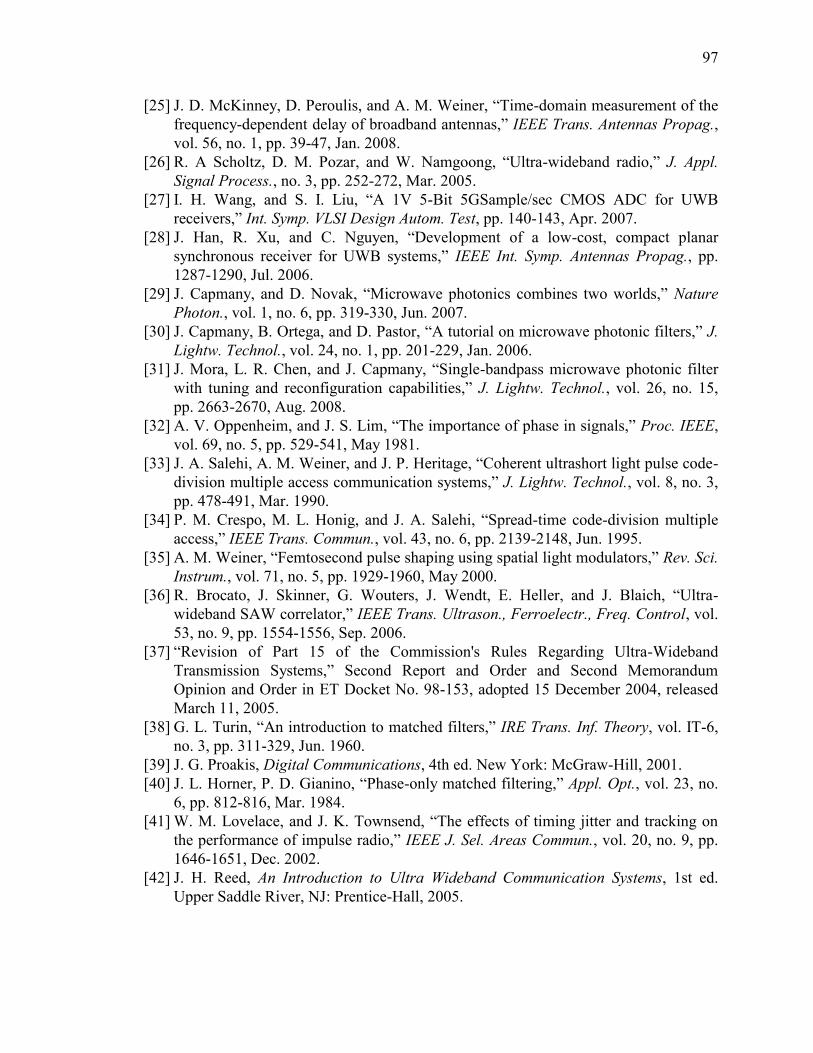
97
[25] J. D. McKinney, D. Peroulis, and A. M. Weiner, “Time-domain measurement of the
frequency-dependent delay of broadband antennas,” IEEE Trans. Antennas Propag.,
vol. 56, no. 1, pp. 39-47, Jan. 2008.
[26] R. A Scholtz, D. M. Pozar, and W. Namgoong, “Ultra-wideband radio,” J. Appl.
Signal Process., no. 3, pp. 252-272, Mar. 2005.
[27] I. H. Wang, and S. I. Liu, “A 1V 5-Bit 5GSample/sec CMOS ADC for UWB
receivers,” Int. Symp. VLSI Design Autom. Test, pp. 140-143, Apr. 2007.
[28] J. Han, R. Xu, and C. Nguyen, “Development of a low-cost, compact planar
synchronous receiver for UWB systems,” IEEE Int. Symp. Antennas Propag., pp.
1287-1290, Jul. 2006.
[29] J. Capmany, and D. Novak, “Microwave photonics combines two worlds,” Nature
Photon., vol. 1, no. 6, pp. 319-330, Jun. 2007.
[30] J. Capmany, B. Ortega, and D. Pastor, “A tutorial on microwave photonic filters,” J.
Lightw. Technol., vol. 24, no. 1, pp. 201-229, Jan. 2006.
[31] J. Mora, L. R. Chen, and J. Capmany, “Single-bandpass microwave photonic filter
with tuning and reconfiguration capabilities,” J. Lightw. Technol., vol. 26, no. 15,
pp. 2663-2670, Aug. 2008.
[32] A. V. Oppenheim, and J. S. Lim, “The importance of phase in signals,” Proc. IEEE,
vol. 69, no. 5, pp. 529-541, May 1981.
[33] J. A. Salehi, A. M. Weiner, and J. P. Heritage, “Coherent ultrashort light pulse code-
division multiple access communication systems,” J. Lightw. Technol., vol. 8, no. 3,
pp. 478-491, Mar. 1990.
[34] P. M. Crespo, M. L. Honig, and J. A. Salehi, “Spread-time code-division multiple
access,” IEEE Trans. Commun., vol. 43, no. 6, pp. 2139-2148, Jun. 1995.
[35] A. M. Weiner, “Femtosecond pulse shaping using spatial light modulators,” Rev. Sci.
Instrum., vol. 71, no. 5, pp. 1929-1960, May 2000.
[36] R. Brocato, J. Skinner, G. Wouters, J. Wendt, E. Heller, and J. Blaich, “Ultra-
wideband SAW correlator,” IEEE Trans. Ultrason., Ferroelectr., Freq. Control, vol.
53, no. 9, pp. 1554-1556, Sep. 2006.
[37] “Revision of Part 15 of the Commission's Rules Regarding Ultra-Wideband
Transmission Systems,” Second Report and Order and Second Memorandum
Opinion and Order in ET Docket No. 98-153, adopted 15 December 2004, released
March 11, 2005.
[38] G. L. Turin, “An introduction to matched filters,” IRE Trans. Inf. Theory, vol. IT-6,
no. 3, pp. 311-329, Jun. 1960.
[39] J. G. Proakis, Digital Communications, 4th ed. New York: McGraw-Hill, 2001.
[40] J. L. Horner, P. D. Gianino, “Phase-only matched filtering,” Appl. Opt., vol. 23, no.
6, pp. 812-816, Mar. 1984.
[41] W. M. Lovelace, and J. K. Townsend, “The effects of timing jitter and tracking on
the performance of impulse radio,” IEEE J. Sel. Areas Commun., vol. 20, no. 9, pp.
1646-1651, Dec. 2002.
[42] J. H. Reed, An Introduction to Ultra Wideband Communication Systems, 1st ed.
Upper Saddle River, NJ: Prentice-Hall, 2005.
98
[43] I. S. Lin, and A. M. Weiner, “Selective correlation detection of photonically-
generated ultra-wideband RF signals,” J. Lightw. Technol., vol. 26, no. 15, pp. 2692-
2699, Aug. 2008.
[44] E. Hamidi, and A. M. Weiner, “Phase-only matched filtering ultrawideband arbitrary
microwave waveforms via optical pulse shaping,” J. Lightw. Technol., vol. 26, no.
15, pp. 2355-2363, Aug. 2008.
[45] J. D. Schwartz, J. Azana, D. V. Plant, “An electronic temporal imaging system for
compression and reversal of arbitrary UWB waveforms,” IEEE Symp. Radio
Wireless, pp. 487-490, Jan. 2008.
[46] J. Y. Lee, and R. A. Scholtz, “Ranging in a dense multipath environment using an
UWB radio link,” IEEE J. Sel. Areas Commun., vol. 20, no. 9, pp. 1677-1683, Dec.
2002.
[47] R. J. Fontana, L. A. Foster, B. Fair, and D. Wu, “Recent advances in ultrawideband
radar and ranging systems,” IEEE Int. Conf. Ultra-Wideband, pp. 19-25, Sep. 2007.
[48] M. Abtahi, M. Mirshafiei, S. LaRochelle, and L. A. Rusch, “All-optical 500 Mb/s
UWB transceiver: an experimental demonstration,” J. Lightw. Technol., vol. 26, no.
15, pp. 2795-2802, Aug. 2008.
[49] J. D. McKinney, I. S. Lin, and A. M. Weiner, “Shaping the power spectrum of
ultrawideband radio-frequency signals,” IEEE Trans. Microw. Theory Tech., vol. 54,
no. 12, pp. 4247-4255, Dec. 2006.
[50] D. Lamensdorf, and L. Susman, “Baseband-pulse-antenna techniques,” IEEE
Antennas Propag. Mag., vol. 36, no. 1, pp. 20-30, Feb. 1994.
[51] A. Shlivinski, E. Heyman, and R. Kastner, “Antenna characterization in the time
domain,” IEEE Trans. Antennas Propag., vol. 45, no. 7, pp. 1140-1149, Jul. 1997.
[52] D. M. Pozar, “Waveform optimizations for ultrawideband radio systems,” IEEE
Trans. Antennas Propag., vol. 51, no. 9, pp. 2335-2345, Sep. 2003.
[53] R. J. Fontana, and E. A. Richley, “Observations on low data rate, short pulse UWB
systems,” IEEE Int. Conf. Ultra-Wideband, pp. 334-338, Sep. 2007.
[54] J. D. Taylor, Ultrawideband Radar Technology, 1st ed. Boca Raton, FL: CRC Press,
2001.
[55] E. Hamidi, and A. M. Weiner, “Post-compensation of ultra-wideband antenna
dispersion using microwave photonic phase filters and its applications to UWB
systems,” IEEE Trans. Microw. Theory Tech., vol. 57, no. 4, pp. 890-898, Apr. 2009.
[56] D. M. Pozar, Microwave Engineering, 3rd ed. New York: Wiley, 2004.
[57] J. S. Hong, and M. J. Lancaster, “Design of highly selective microstrip bandpass
filters with a single pair of attenuation poles at finite frequencies,” IEEE Trans.
Microw. Theory Tech., vol. 48, no. 7, pp. 1098-1107, Jul. 2000.
[58] G. Tsuzuki, S. Ye, and S. Berkowitz, “Ultra-selective 22-pole 10-transmission zero
superconducting bandpass filter surpasses 50-pole Chebyshev filter,” IEEE Trans.
Microw. Theory Tech., vol 50, no. 12, pp. 2924-2929, Dec. 2002.
[59] H. Joshi, H. H. Sigmarsson, S. Moon, D. Peroulis, and W. J. Chappell, “High-Q fully
reconfigurable tunable bandpass filters,” IEEE Trans. Microw. Theory Tech., vol. 57,
no. 12, pp. 3525-3533, Dec. 2009.
99
[60] S. J. Park, I. Reines, C. Patel, and G. M. Rebeiz, “High-Q RF-MEMS 4-6-GHz
tunable evanescent-mode cavity filter,” IEEE Trans. Microw. Theory Tech., vol. 58,
no. 2, pp. 381-389, Feb. 2010.
[61] E. Hamidi, D. E. Leaird, and A. M. Weiner, “Tunable programmable microwave
photonic filters based on an optical frequency comb,” IEEE Trans. Microw. Theory
Tech., vol. 58, no. 11, pp. 3269-3278, Nov. 2010.
[62] M. Shirasaki, “Large angular dispersion by a virtually imaged phased array and its
application to a wavelength demultiplexer,” Opt. Lett., vol. 21, no. 5, pp. 366-368,
Mar. 1996.
[63] S. Xiao, A. M. Weiner, and C. Lin, “A dispersion law for virtually imaged phased-
array spectral dispersers based on paraxial wave theory,” IEEE J. Quantum
Electron., vol. 40, no. 4, pp. 420-426, Apr. 2004.
[64] B. M. Jung, J. D. Shin, and B. G. Kim, “Optical true time-delay for two-dimensional
X-band phased array antennas,” IEEE Photon. Technol. Lett., vol. 19, no. 12, pp.
877-879, Jun. 2007.
[65] A. M. Weiner, Ultrafast Optics, 1st ed. New York: Wiley, 2009.
[66] C. B. Huang, Z. Jiang, D. E. Leaird, and A. M. Weiner, “The impact of optical comb
stability on waveforms generated via spectral line-by-line pulse shaping,” Opt. Exp.,
vol. 14, no. 26, pp. 13164-13176, Dec. 2006.
[67] W. S. C. Chang, RF Photonic Technology in Optical Fiber Links, 1st ed. Cambridge,
U. K.: Cambridge Univ. Press, 2002.
[68] M. L. Farwell, W. S. C. Chang, and D. R. Huber, “Increased linear dynamic range by
low biasing the Mach-Zehnder modulator,” IEEE Photon. Technol. Lett., vol. 5, no.
7, pp. 779-782, Jul. 1999.
[69] Z. Jiang, D. E. Leaird, and A. M. Weiner, “Optical arbitrary waveform generation
and characterization using spectral line-by-line control,” J. Lightw. Technol., vol. 24,
no. 7, pp. 2487-2494, Jul. 2006.
[70] C. B. Huang, S. G. Park, D. E. Leaird, and A. M. Weiner, “Nonlinearly broadened
phase-modulated continuous-wave laser frequency combs characterized using DPSK
decoding,” Opt. Exp., vol. 16, no. 4, pp. 2520-2527, Feb. 2008.
[71] Z. Jiang, C. B. Huang, D. E. Leaird, and A. M. Weiner, “Optical arbitrary waveform
processing of more than 100 spectral comb lines,” Nature Photon., vol. 1, pp. 463-
467, Aug. 2007.
[72] K. Takano, Y. Naganuma, and K. Nakagawa, “Performance analysis of optical single
sideband modulation based on Mach-Zehnder interferometers and its dispersive fiber
transmission,” IEICE Trans. Commun., vol. E88–B, no. 5, pp. 1994-2003, May
2005.
[73] J. Capmany, B. Ortega, D. Pastor, and S. Sales, “Discrete-time optical processing of
microwave signals,” J. Lightw. Technol., vol. 23, no. 2, pp. 702-723, Feb. 2005.
[74] A. V. Oppenheim, and R. W. Schafer, Discrete-Time Signal Processing, 3rd ed.
Englewood Cliffs, NJ: Prentice-Hall, 2009.
[75] J. D. McKinney, and K. J. Williams, “Sampled analog optical links,” IEEE Trans.
Microw. Theory Tech., vol. 57, no. 8, pp. 2093-2099, Aug. 2009.
100
[76] V. R. Supradeepa, D. E. Leaird, and A. M. Weiner, “Optical arbitrary waveform
characterization via dual-quadrature spectral interferometry,” Opt. Exp., vol. 17, no.
1, pp. 25-33, Jan. 2009.
[77] H. Miao, D. E. Leaird, C. Langrock, M. M. Fejer, and A. M. Weiner, “Optical
arbitrary waveform characterization via dual-quadrature spectral shearing
interferometry,” Opt. Exp., vol. 17, no. 5, pp. 3381-3389, Mar. 2009.
[78] J. D. McKinney, M. Godinez, V. J. Urick, S. Thaniyavarn, W. Charczenko, and K. J.
Williams, “Sub-10-dB noise figure in a multiple-GHz analog optical link,” IEEE
Photon. Technol. Lett., vol. 19, no. 7, pp. 465-467, Apr. 2007.
[79] C. Middleton, and R. Desalvo, “High performance microwave photonic links using
double sideband suppressed carrier modulation and balanced coherent heterodyne
detection,” Proc. IEEE Military Commun. Conf., pp. 124-129, 2009.
[80] F. Devaux, Y. Sorel, and J. F. Kerdiles, “Simple measurement of fiber dispersion and
of chirp parameter of intensity modulated light emitter,” J. Lightw. Technol., vol 11,
no. 12, pp. 1937-1940, Dec. 1993.
[81] R. Wu, V. R. Supradeepa, C. M. Long, D. E. Leaird, and A. M. Weiner, “Generation
of very flat optical frequency combs from continuous wave lasers using cascaded
intensity and phase modulators driven by tailored radio frequency waveforms,” Opt.
Lett., vol. 35, no. 19, pp. 3234-3236, Oct. 2010.
[82] L. T. Nichols, K. J. Williams, and R. D. Esman, “Optimizing the ultrawide-band
photonic link,” IEEE Trans. Microw. Theory Tech., vol. 45, no. 8, pp. 1384-1389,
Aug. 1997.
[83] Y. Shi, C. Zhang, H. Zhang, J. H. Bechtel, L. R. Dalton, B. H. Robinson, and W. H.
Steier, “Low (sub-1-volt) halfwave voltage polymeric electro-optic modulators
achieved by controlling chromophore shape,” Science, vol. 288, no. 5463, pp. 119-
122, Apr. 2000.
[84] V. J. Urick, M. S. Rogge, F. Bucholtz, and K. J. Williams, “Wideband (0.045-6.25
GHz) 40km analogue fibre-optic link with ultra-high (>40 dB) all-photonic gain,”
Electron. Lett., vol. 42, no. 9, pp. 552-553, Apr. 2006.
[85] M. J. R. Heck, P. Munoz, B. W. Tilma, E. A. J. M. Bente, Y. Barbarin, Y. S. Oei, R.
Notzel, and M. K. Smit, “Design, fabrication and characterization of an InP-based
tunable integrated optical pulse shaper,” IEEE J. Quantum Electron., vol. 44, no. 4,
pp. 370-377, Apr. 2008.
[86] D. A. Tulchinsky, J. B. Boos, P. Doewon, P. G. Goetz, W. S. Rabinovich, and K. J.
Williams, “High-current photodetectors as efficient, linear, and high-power RF
output stages,” J. Lightw. Technol., vol. 26, no. 4, pp. 408-416, Feb. 2008.
[87] D. A. B. Miller, “Rationale and challenges for optical interconnects to electronic
chips,” Proc. IEEE, vol. 88, no. 6, pp. 728-749, Jun. 2000.
[88] B. Jalali and S. Fathpour, “Silicon photonics,” J. Lightw. Technol., vol. 24, no. 12,
pp. 4600-4615, Dec. 2006.
[89] D. Dai, A. Fang, and J. E Bowers, “Hybrid silicon lasers for optical interconnects,”
New J. Physics, vol. 11, 125016-125032, Dec. 2009.
[90] H. Rong, R. Jones, A. Liu, O. Cohen, D. Hak, A. Fang and M. Paniccia, “A
continuous-wave Raman silicon laser,” Nature, vol. 433, pp. 725-728, Feb. 2005.

101
[91] S. Manipatruni, K. Preston, L. Chen, and M. Lipson, “Ultra-low voltage, ultra-small
mode volume silicon microring modulator,” Opt. Exp., vol. 18, no. 17, pp. 18235-
18242, Aug. 2010.
[92] P. Cheben, J. H. Schmid, A. Delage, A. Densmore, S. Janz, B. Lamontagne, J.
Lapointe, E. Post, P. Waldron, and D. X. Xu, “A high-resolution silicon-on-insulator
arrayed waveguide grating microspectrometer with sub-micrometer aperture
waveguides,” Opt. Exp., vol. 15, no. 5, pp. 2299-2306, Mar. 2007.
[93] J. Van Campenhout, W. M. Green, and Y. A. Vlasov, “Design of a digital, ultra-
broadband electro-optic switch for reconfigurable optical networks-on-chip,” Opt.
Exp., vol. 17, no. 26, pp. 23793-23808, Dec. 2009.
[94] F. Horst, W. M. J. Green, B. J. Offrein, and Y. A. Vlasov, “Silicon-on-insulator
echelle grating WDM demultiplexers with two stigmatic points,” IEEE Photon.
Technol. Lett., vol. 21, no. 23, pp. 1743-1745, Dec. 2009.
[95] S. Assefa, F. Xia, and Y. A. Vlasov, “Reinventing nanophotonic avalanche
photodetector for on chip optical interconnects,” Nature, vol. 464, pp. 80-84, Mar.
2010.
[96] M. S. Rasras, K. Y. Tu, D. M. Gill, Y. K. Chen, A. E. White, S. S. Patel, A.
Pomerene, D. Carothers, J. Beattie, M. Beals, J. Michel, and L. C. Kimerling,
“Demonstration of a tunable microwave-photonic notch filter using low-loss silicon
ring resonators,” J. Lightw. Technol., vol. 27, no. 12, pp. 2105-2110, Jun. 2009.
[97] T. E. Darcie and P. F. Driessen, “Class-AB techniques for high-dynamic-range
microwave photonic links,” IEEE Photon. Technol. Lett., vol. 18, no. 8, pp. 929-931,
Apr. 2006.
[98] V. J. Urick, F. Bucholtz, P. S. Devgan, J. D. McKinney, and K. J. Williams, “Phase
modulation with interferometric detection as an alternative to intensity modulation
with direct detection for analog-photonic links,” IEEE Trans. Microw. Theory Tech.,
vol. 55, no. 9, pp. 1978-1985, Sep. 2007.
[99] V. R. Supradeepa, C. B. Huang, D. E. Leaird, and A. M. Weiner, “Femtosecond
pulse shaping in two dimensions: towards higher complexity optical waveforms,”
Opt. Exp., vol. 16, no. 16, pp. 11878-11887, Aug. 2008.
[100] H. Liu, “Multicode ultra-wideband scheme using chirp waveforms,” IEEE J. Sel.
Areas Commun., vol. 24, no. 4, pp. 885-891, Apr. 2006.
[101] B. Vidal, V. Polo, J. L. Corral, and J. Marti, “Harmonic suppressed photonic
microwave filter,” J. Lightw. Technol., vol. 21, no. 12, pp. 3150-3154, Dec. 2003.
[102] Y. Yan, and J. Yao, “Photonic microwave bandpass filter with improved dynamic
range,” Opt. Lett., vol. 33, no. 15, pp. 1756-1758, Aug. 2008.
[103] F. J. Harris, “On the use of windows for harmonic analysis with the discrete
Fourier transform,” Proc. IEEE, vol. 66, no. 1, pp. 51-83, Jan. 1978.
[104] D. Cassioli, M. Z. Win, F. Vatalaro, and A. F. Molisch, “Low complexity Rake
receivers in ultra-wideband channels,” IEEE Trans. Wireless Commun., vol. 6, no. 4,
pp. 1265-1274, Apr. 2007.

APPENDICES
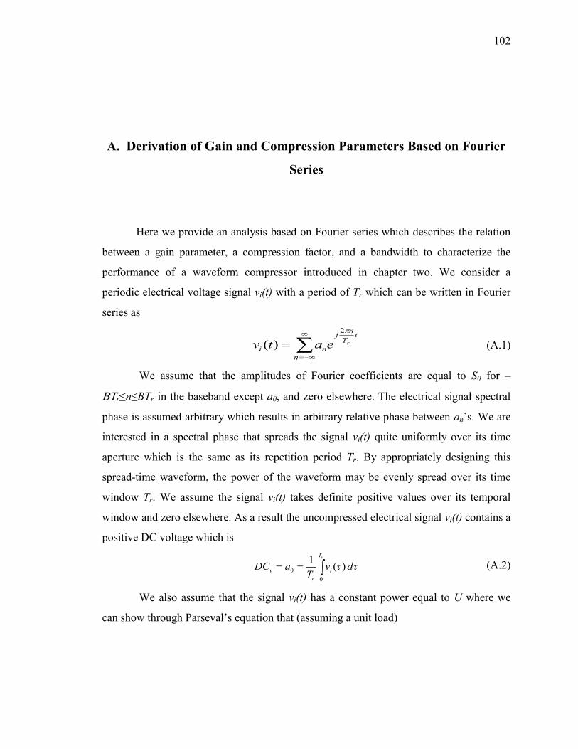
102
A. Derivation of Gain and Compression Parameters Based on Fourier
Series
Here we provide an analysis based on Fourier series which describes the relation
between a gain parameter, a compression factor, and a bandwidth to characterize the
performance of a waveform compressor introduced in chapter two. We consider a
periodic electrical voltage signal vi(t) with a period of Tr which can be written in Fourier
series as
n
tT
nj
nireatv
2
)( (A.1)
We assume that the amplitudes of Fourier coefficients are equal to S0 for –
r≤n≤BTr in the baseband except a0, and zero elsewhere. The electrical signal spectral
phase is assumed arbitrary which results in arbitrary relative phase between an’s. We are
interested in a spectral phase that spreads the signal vi(t) quite uniformly over its time
aperture which is the same as its repetition period Tr. By appropriately designing this
spread-time waveform, the power of the waveform may be evenly spread over its time
window Tr. We assume the signal vi(t) takes definite positive values over its temporal
window and zero elsewhere. As a result the uncompressed electrical signal vi(t) contains a
positive DC voltage which is
rT
i
r
v dvT
aDC0
0 )(1
(A.2)
We also assume that the signal vi(t) has a constant power equal to U where we
can show through Parseval’s equation that (assuming a unit load)
103
rT
i
r
m
mn
n dttvT
aU0
22 |)(|1
|| (A.3)
Also we have
2
0
2
0
2 2|| amSam
mn
n
(A.4)
where
rBTm (A.5)
From foregoing assumptions we can write
k
r
n
tT
nj
nt
kTtBSSaea r
)](2sin[)(|| 000
2
(A.6)
By substituting (A.6) in (2.11) we find an expression for the output compressed
electrical voltage
2
0002
022 )](2sin[
)(2
1)(
k
rbiaso
t
nTtBSSaVVeLtv
(A.7)
Then we find the compressed pulse peak voltage as
002 amSVVV biasc (A.8)
The DC level of the output compressed pulse voltage over its temporal window
can be approximated as
2
0
2
0
22 )(2
1aVVeLDC biasc (A.9)
The term Vbias-V can be made negligible by biasing the IM close to its minimum
transmission. For an input electrical waveform that spreads extensively enough over time
the resulting output uncompressed signal DC voltage over its time window will be much
smaller than the output compressed waveform peak voltage, in other words
VVamS bias 002 (A.10)
Thus we can show through (A.7) that the compressed pulse FWHM duration tc is
approximately given by
B
tc
44.0 (A.11)
104
Defining the maximum peak voltage of vi(t) as Vp, we write the output
uncompressed waveform peak voltage as
22
0
22 )(2
1 VVVeLV biaspu (A.12)
Finally by substituting in the gain parameter expression, we will obtain
rT
biasi
r
biasp
bias
dVVvT
VVV
aVVmSmS
0
22
000
])([1
)(
)(4
(A.13)
In order to achieve further intuition into (A.13), we provide an approximate
analytical solution for a simple case. We assume vi(t) as a linear frequency-modulated
signal with a period of Tr which is given over –r/2≤t≤Tr/2 by
1
2cos
2)(
2
r
w
p
i
Tt
T
BVtv (A.14)
If the signal time-bandwidth product is much larger than one, or in other words
there are many oscillations in the signal temporal window then we can approximate the
integral in (A.13) as below
22
0
2
28])([
1
VV
VVdVVv
Tbias
pp
T
biasi
r
r
(A.15)
For U from (A.4) we have
8
3|)(|
12
0
2 p
T
i
r
Vdttv
TU
r
(A.16)
The DC level of signal vi(t) is given by
2
)(1
0
0
p
T
i
r
v
Vdv
TaDC
r
(A.17)
Then we can find S0 by substituting for a0 and U in (A.4) as
r
p
BT
VS
40 (A.18)
By substituting for S0 in (A.13) we find the gain parameter

105
22
2
28)(
24
p
bias
p
biasp
p
bias
pr
pr
VVV
VVVV
VVV
VBTVBT
(A.19)
After simplification we rewrite it as
p
bias
p
biasr
r
V
VV
V
VVBTBT
8
5
4
2
(A.20)
This expression shows that the theoretical gain parameter for a linear chirp signal
is decreasing by increasing Vbias-V and it takes its maximum value for Vbias=V. For
Vbias=V which corresponds to a bias point at the minimum transmission of the modulator
we define the maximum gain parameter 0
rr BTBT
5
4
5
20 (A.21)
By substituting for B we finally obtain
531.0176.00 (A.22)
Equations (A.21) and (A.22) show that for large values of compression factor, i.
e., an input chirp waveform has a large time-bandwidth product, the maximum gain
parameter becomes approximately proportional to compression factor with a factor of
0.176. This expression gives us a rough estimate of an achievable gain parameter versus
compression factor.
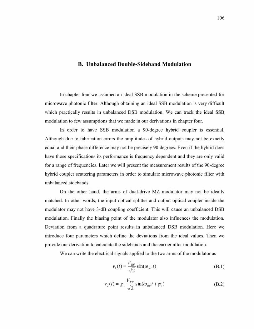
106
B. Unbalanced Double-Sideband Modulation
In chapter four we assumed an ideal SSB modulation in the scheme presented for
microwave photonic filter. Although obtaining an ideal SSB modulation is very difficult
which practically results in unbalanced DSB modulation. We can track the ideal SSB
modulation to few assumptions that we made in our derivations in chapter four.
In order to have SSB modulation a 90-degree hybrid coupler is essential.
Although due to fabrication errors the amplitudes of hybrid outputs may not be exactly
equal and their phase difference may not be precisely 90 degrees. Even if the hybrid does
have those specifications its performance is frequency dependent and they are only valid
for a range of frequencies. Later we will present the measurement results of the 90-degree
hybrid coupler scattering parameters in order to simulate microwave photonic filter with
unbalanced sidebands.
On the other hand, the arms of dual-drive MZ modulator may not be ideally
matched. In other words, the input optical splitter and output optical coupler inside the
modulator may not have 3-dB coupling coefficient. This will cause an unbalanced DSB
modulation. Finally the biasing point of the modulator also influences the modulation.
Deviation from a quadrature point results in unbalanced DSB modulation. Here we
introduce four parameters which define the deviations from the ideal values. Then we
provide our derivation to calculate the sidebands and the carrier after modulation.
We can write the electrical signals applied to the two arms of the modulator as
)sin(2
)(1 tV
tv RFRF (B.1)
)sin(2
)(2 vRFRF
v tV
tv (B.2)

107
where v is the amplitude imbalance between two electrical signals and ideally it equals
to one. v is the phase difference between two electrical signals and ideally it equals to 90
degrees.
Assuming a CW input to the modulator, we can write the modulator output optical
electric field as
mjV
tvjtj
m
V
tvjtj
eee
te
)()(
0
21
2)( (B.3)
where e0 and are the modulator input electric field amplitude and angular frequency, m
is the amplitude imbalance between two waveguides and ideally it equals to one. m is the
phase corresponding to the modulator bias point which it ideally equals to 90 degrees for
biasing at quadrature point. By substituting v1(t) and v2(t) into (B.3) we can rewrite it as
mvRFRF
vRFRF jt
V
Vj
m
tV
Vj
tj eeee
te
)sin(
2)sin(
20
2)( (B.4)
To the first order approximation for small values of VRF/√2V we can simplify
(B.4) as
)sin(
21)sin(
21
2)( 0
vRFRF
v
j
mRFRFtj t
V
Vjet
V
Vje
ete m
(B.5)
Now we find the carrier as
)1(2
)( 0 mj
m
tj
c eee
te (B.6)
We also find the positive and negative sidebands respectively as
)()(0 124
)( vmRF j
vm
tjRF
s eeV
Vete
(B.7)
)()(0 124
)( vmRF j
vm
tjRF
s eeV
Vete
(B.8)
The terms in the brackets in (B.6), (B.7) and (B.8) give the amplitude and phase of
sidebands and the carrier as a function of parameters which we have defined. For ideal
values of m=1, v=1, m= andv= we have
108
tj
c ee
jte
2)1()( 0 (B.9)
0)( tes (B.10)
tjRF
sRFe
V
Vete
)(0
22)(
(B.11)
By biasing the modulator at opposite quadrature the phase m can be set to -
where the negative sideband will vanish and the positive sideband will appear. In other
words
tj
c ee
jte
2)1()( 0 (B.12)
tjRF
sRFe
V
Vete
)(0
22)(
(B.13)
0)( tes (B.14)
After propagation through the dispersive fiber we can write the electric fields of
(B.6), (B.7) and (B.8) as
)1(2
)( )(0 mj
m
jtj
c eee
te
(B.15)
)()()(0 124
)( vmRFRF j
vm
jtjRF
s eeV
Vete
(B.16)
)()()(0 124
)( vmRFRF j
vm
jtjRF
s eeV
Vete
(B.17)
where the chromatic dispersion is given by (4.5). We write the PD current as
2
)()( teti (B.18)
The terms generating current at the frequency of ±RF are given by
..)()()()()( ccteteteteti scsc
(B.19)
Then
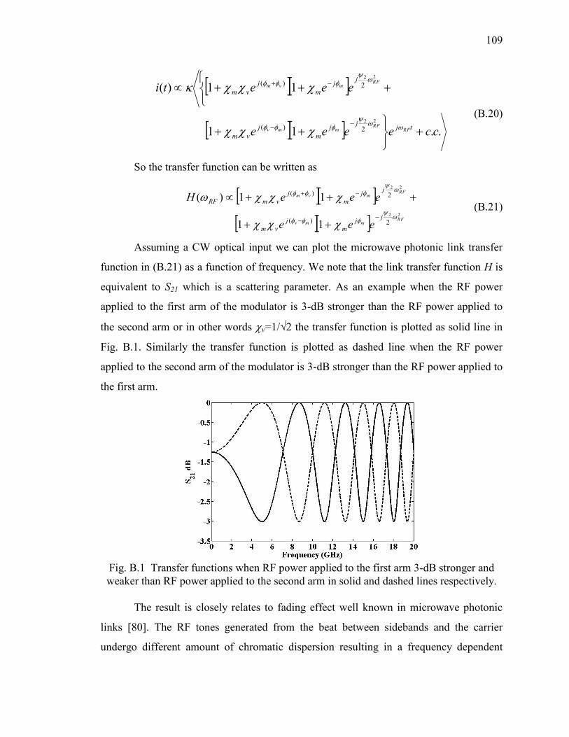
109
..11
11)(
22
22
2)(
2)(
cceeee
eeeti
tjj
j
m
j
vm
jj
m
j
vm
RFRF
mmv
RFmvm
(B.20)
So the transfer function can be written as
22
22
2)(
2)(
11
11)(
RFmmv
RFmvm
jj
m
j
vm
jj
m
j
vmRF
eee
eeeH
(B.21)
Assuming a CW optical input we can plot the microwave photonic link transfer
function in (B.21) as a function of frequency. We note that the link transfer function H is
equivalent to S21 which is a scattering parameter. As an example when the RF power
applied to the first arm of the modulator is 3-dB stronger than the RF power applied to
the second arm or in other words v=1/√2 the transfer function is plotted as solid line in
Fig. B.1. Similarly the transfer function is plotted as dashed line when the RF power
applied to the second arm of the modulator is 3-dB stronger than the RF power applied to
the first arm.
Fig. B.1 Transfer functions when RF power applied to the first arm 3-dB stronger and
weaker than RF power applied to the second arm in solid and dashed lines respectively.
The result is closely relates to fading effect well known in microwave photonic
links [80]. The RF tones generated from the beat between sidebands and the carrier
undergo different amount of chromatic dispersion resulting in a frequency dependent

110
interference. This interference appears as an amplitude variation in the transfer function
that its swing relates to the relative intensity of two sidebands. This variation becomes
faster for higher frequencies since the chromatic dispersion is quadratically dependent on
frequency.
Now we plot the transfer function when the contribution of the second arm optical
power at the output is 3-dB weaker than the one from the first arm, or in other words
m=1/√2, as solid in Fig. B.2. Similarly we plot the transfer function when the
contribution of the second arm optical power at the output is 3-dB stronger than the one
from the first arm as dashed line.
Fig. B.2 Transfer functions when optical power in the second arm is 3-dB weaker and
stronger in solid and dashed lines respectively.
Now we plot the transfer function when the phase difference between the RF
signals applied to the two arms is 100 degrees, or in other words v=5, as solid in Fig.
B.3. Similarly we plot transfer function when the phase difference between the RF signals
applied to the two arms is 80 degrees, or in other wordsv=4as dashed line. The
transfer function illustrates similar effect as in Fig. B.3 for biasing the modulator away
from a quadrature point.
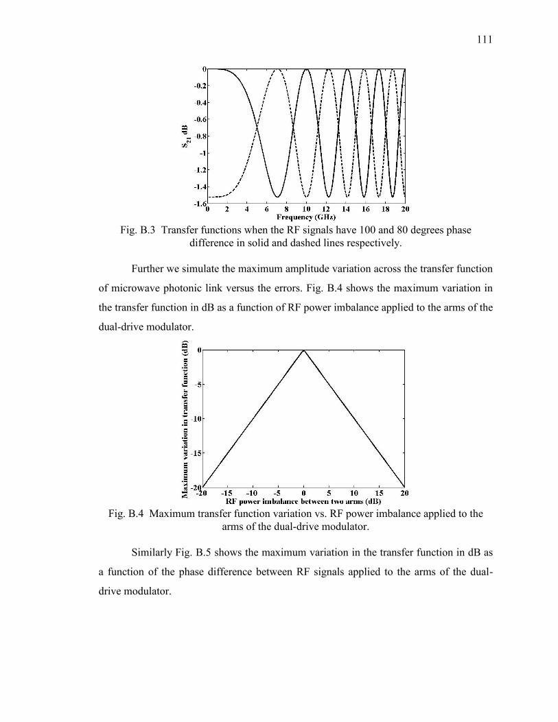
111
Fig. B.3 Transfer functions when the RF signals have 100 and 80 degrees phase
difference in solid and dashed lines respectively.
Further we simulate the maximum amplitude variation across the transfer function
of microwave photonic link versus the errors. Fig. B.4 shows the maximum variation in
the transfer function in dB as a function of RF power imbalance applied to the arms of the
dual-drive modulator.
Fig. B.4 Maximum transfer function variation vs. RF power imbalance applied to the
arms of the dual-drive modulator.
Similarly Fig. B.5 shows the maximum variation in the transfer function in dB as
a function of the phase difference between RF signals applied to the arms of the dual-
drive modulator.

112
Fig. B.5 Maximum transfer function variation vs. phase difference between RF signals
applied to the arms of the dual-drive modulator.
In the next step we measure the hybrid scattering parameters and we use these
parameters to find the frequency dependent amplitude imbalance between two electrical
signals, v and phase difference between two electrical signals v. We use a VNA to
measure the scattering parameters from the input to each of the output ports while the rest
of the ports are terminated with matched loads. The black and grey plots in Fig. B.6 show
the amplitudes of transmission from the input to the 0 and 90-degree ports of the hybrid
respectively. As we expect over the frequency range of 1 to 12.4 GHz the hybrid
transmission closely equals to -3 dB.
Fig. B.6 Amplitude frequency responses of hybrid’s 0 and 90-degree ports in black and
grey respectively.

113
In Fig. B.7 we plot the nonlinear part of scattering parameters’ phases. The black
and grey plots show the phases of transmission from the input to the 0 and 90-degree
ports of the hybrid respectively. As we expect over the frequency range of 1 to 12.4 GHz
the phase difference between ports remains about 90 degrees.
Fig. B.7 Phase frequency responses of hybrid’s 0 and 90-degree ports in black and grey
respectively.
Now we measure the RF photonic link transfer function. We use a CW laser
connected to the modulator which is driven by the 90-degree hybrid. The output is
dispersed through a 60-km SMF and after amplification in an EDFA the output is
detected using a PD. The transmission shown in Fig. B.8 is measured using a VNA.
Fig. B.8 Measured transfer function of the microwave photonic link with 60-km SMF.
We note that the dips at 15 and 18.5 GHz are the signatures of DSB modulation
with fading effect. For frequencies out of 1 to 12.4 GHz the performance of hybrid
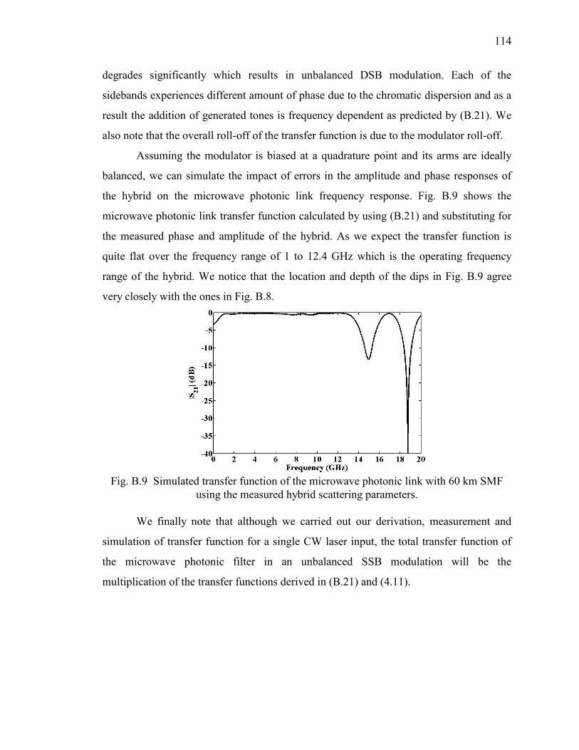
114
degrades significantly which results in unbalanced DSB modulation. Each of the
sidebands experiences different amount of phase due to the chromatic dispersion and as a
result the addition of generated tones is frequency dependent as predicted by (B.21). We
also note that the overall roll-off of the transfer function is due to the modulator roll-off.
Assuming the modulator is biased at a quadrature point and its arms are ideally
balanced, we can simulate the impact of errors in the amplitude and phase responses of
the hybrid on the microwave photonic link frequency response. Fig. B.9 shows the
microwave photonic link transfer function calculated by using (B.21) and substituting for
the measured phase and amplitude of the hybrid. As we expect the transfer function is
quite flat over the frequency range of 1 to 12.4 GHz which is the operating frequency
range of the hybrid. We notice that the location and depth of the dips in Fig. B.9 agree
very closely with the ones in Fig. B.8.
Fig. B.9 Simulated transfer function of the microwave photonic link with 60 km SMF
using the measured hybrid scattering parameters.
We finally note that although we carried out our derivation, measurement and
simulation of transfer function for a single CW laser input, the total transfer function of
the microwave photonic filter in an unbalanced SSB modulation will be the
multiplication of the transfer functions derived in (B.21) and (4.11).

115
C. Derivation of Radio Frequency Photonic Filters Gain
Here we provide the derivation of microwave photonic filters’ gain discussed in
chapter four. Although we will carry out the derivations for a single optical tone as a
source rather than an optical comb, we can show that the RF gains derived in this
appendix correspond to the maximum peak of the filter passband where the powers of all
taps constructively add in-phase.
Fig. C.1 Model for microwave photonic filter based on an IM.
Fig. C.1 shows our model for a filter configuration based on an IM. An RF tone
with power of PRF with an angular frequency of RF is driving an IM which is biased at a
quadrature point, Vbias=V/2 where V is the half-wave voltage. We write the input
electrical signal into the modulator as
)cos()( tVtv RFRFin (C.1)
An optical source with an optical power of PS is connected to an optical pulse
shaper with an optical loss of LPS and then its output is amplified by an optical amplifier
with a gain of GA. We write the electric field of the optical source with an angular
frequency of as
tj
ss ePta )( (C.2)
We assume the modulator optical insertion loss is LM. Then we can write the
optical output of the modulator as
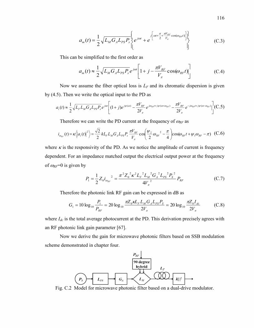
116
)cos(
2
2
1)(
tV
Vtj
tj
sPSAMm
RFRF
eePLGLta
(C.3)
This can be simplified to the first order as
)cos(1
2
1)( t
V
VjePLGLta RF
RFtj
sPSAMm
(C.4)
Now we assume the fiber optical loss is LF and its chromatic dispersion is given
by (4.5). Then we write the optical input to the PD as
)()()(
22)1(
2
1)( RFRFRFRF jtjRFjtjRFjtj
sPSAMFi eV
Ve
V
VejePLGLLta
(C.5)
Therefore we can write the PD current at the frequency of RF as
)cos(42
cos2
2)()( 1
222
RFRFRF
RF
sPSAMFi tV
VPLGLkLtati
RF
(C.6)
where is the responsivity of the PD. As we notice the amplitude of current is frequency
dependent. For an impedance matched output the electrical output power at the frequency
of RF=0 is given by
RF
SPSAMF PV
PLGLLZiZP
RF 2
2222222
0
22
0142
1
(C.7)
Therefore the photonic link RF gain can be expressed in dB as
V
IZ
V
PLGLLZ
P
PG dcSPSAMF
RF 2log20
2log20log10 0
10
0
10
1
101 (C.8)
where Idc is the total average photocurrent at the PD. This derivation precisely agrees with
an RF photonic link gain parameter [67].
Now we derive the gain for microwave photonic filters based on SSB modulation
scheme demonstrated in chapter four.
Fig. C.2 Model for microwave photonic filter based on a dual-drive modulator.
117
An RF tone with power of PRF with an angular frequency of RF is split into two
RF signals with 90 degree phase difference. Assuming an ideal hybrid the loss from input
port to the output ports equals to 3 dB. Each of the two outputs is driving one arm of the
dual-drive modulator which is biased at a quadrature point, Vbias=V/2. We can write the
input electrical signal into the 90-degree hybrid as
)cos()( tVtv RFRFin (C.9)
Then we can write the RF electrical signals to arms of modulator as
)sin(2
)(1 tV
tv RFRF (C.10)
)cos(2
)(2 tV
tv RFRF (C.11)
We assume the optical source electric field similar as before. Then we can write
the optical output of the modulator as
)cos(
22)sin(
2
2
1)(
tV
Vtjt
V
Vtj
sPSAMm
RFRF
RFRF
eePLGLta
(C.12)
This can be simplified to the first order as
tjRFtj
sPSAMmRFe
V
VjePLGLta
21
2
1)( (C.13)
Now the optical input into the PD can be written as
)()(
2)1(
2
1)( RFRF jtjRFjtj
sPSAMFi eV
VejePLGLLta
(C.14)
Then we can write the PD current at the frequency of RF as
42cos
2
1)()( 1
222
RFRFRF
RF
sPSAMFi tV
VPLGLLtati
RF
(C.15)
For an impedance matched output the electrical power in the first harmonic at the
output is given by

118
RF
SPSAMF PV
PLGLLZiZP
RF 2
2222222
0
22
0142
1
(C.16)
As we notice the electrical power in the first harmonic derived in (C.16) exactly
equals to the electrical power found in (C.6). Hence the RF photonic link gain for a SSB
modulation also is given by (C.8).
Now we derive the gain for tunable RF photonic filters based on interferometric
scheme demonstrated in chapter four. As it shown in Fig. C.3 we model the DPSK
demodulator as an ideal optical filter which only suppresses the carriers in the modulated
path. Therefore at the PD the sidebands from the modulated path and the comb lines in
the delayed path beat. Here we assume 3-dB optical splitter and coupler which result in
the maximum RF photonic gain.
Fig. C.3 Model for tunable RF photonic filter based on SSB modulation and
interferometric scheme.
Similarly we can write the optical output of the modulator as
)cos(
22)sin(
2
22
1)(
tV
Vtjt
V
Vtj
sPSAMm
RFRF
RFRF
eePLGLta
(C.17)
This can be simplified to the first order as
tjRFtj
sPSAMmRFe
V
VjePLGLta
21
22
1)( (C.18)
After the optical filter we assume the carriers are thoroughly suppressed. Hence its
output can be written as
tj
sPSAMRF
mRFePLGL
V
Vta
)(
4)(
(C.19)
Now we can write the optical input into the PD as
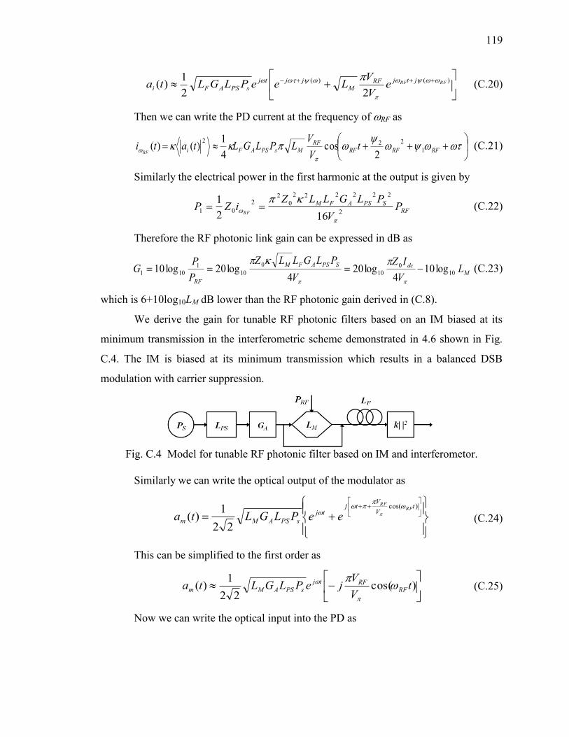
119
)()(
22
1)( RFRF jtjRF
M
jjtj
sPSAFi eV
VLeePLGLta
(C.20)
Then we can write the PD current at the frequency of RF as
RFRFRF
RF
MsPSAFi tV
VLPLGLtati
RF 1
222
2cos
4
1)()( (C.21)
Similarly the electrical power in the first harmonic at the output is given by
RF
SPSAFM PV
PLGLLZiZP
RF 2
222222
0
22
01162
1
(C.22)
Therefore the RF photonic link gain can be expressed in dB as
M
dcSPSAFM
RF
LV
IZ
V
PLGLLZ
P
PG 10
0
10
0
101
101 log104
log204
log20log10
(C.23)
which is 6+10log10LM dB lower than the RF photonic gain derived in (C.8).
We derive the gain for tunable RF photonic filters based on an IM biased at its
minimum transmission in the interferometric scheme demonstrated in 4.6 shown in Fig.
C.4. The IM is biased at its minimum transmission which results in a balanced DSB
modulation with carrier suppression.
Fig. C.4 Model for tunable RF photonic filter based on IM and interferometor.
Similarly we can write the optical output of the modulator as
)cos(
22
1)(
tV
Vtj
tj
sPSAMm
RFRF
eePLGLta
(C.24)
This can be simplified to the first order as
)cos(
22
1)( t
V
VjePLGLta RF
RFtj
sPSAMm
(C.25)
Now we can write the optical input into the PD as

120
)()()(
4
2
1)(
RFRFRFRF jtjjtjRFM
jj
tj
sPSAFi
eeV
VLje
ePLGLta
(C.26)
Then we can write the PD current at the frequency of RF as
)cos(2
sin4
1)()( 1
222
RFRFRF
RF
MsPSAMFi tV
VLPLGLLtati
RF
(C.27)
We can rewrite (C.27) as
22
1
22
12
sin2
sin
8
1)(
RFRFRFRFRFRF
RF
MsPSAMF
tt
V
VLPLGLLti
RF
(C.28)
We notice that two sine terms in brackets have a phase argument dependent on
delay with an opposite sign. Each of those terms contributes to a different bandpass as
derived in (4.26). Hence the electrical power in the first harmonic at the output
contributing to one passband is given by
RF
SPSAFM PV
PLGLLZiZP
2
222222
0
22
101642
1
(C.29)
Therefore the RF photonic link gain can be expressed in dB as
M
dcSPSAFM
RF
LV
IZ
V
PLGLLZ
P
PG 10
0
10
0
10
1
101 log108
log208
log20log10
(C.30)
which is 12+10log10LM dB lower than the RF photonic gain derived in (C.8).

121
D. Simulation of Apodized Multitap Filters
Here we briefly discuss simulation results based on the theoretical transfer
function (4.11) calculated numerically in MATLAB and investigate the impact of
apodization of tap weights on filter parameters such as SLS and 3-dB BW. To
demonstrate the potential of these filters to achieve high SLS, we simulate the transfer
functions of filters with two tap weight apodizations. We assume the comb source
spacing equals to 10 GHz at 1550 nm with 100 comb lines and we assume a perfect SSB
modulation. We choose the length of dispersive fiber such that we can obtain 100-ps
delay spacing between taps.
First we assume that the comb spectral lines have a uniform intensity or in other
words the tap weights are equal which is plotted in Fig. D.1(a). The simulated bandpass
filter is shown in grey line in Fig. D.1(c). The center of bandpass filter is set at 2.5 GHz
by applying an incremental phase across taps in steps of /2.
As we expect the filter has the shape of a sinc function with about 13-dB SLS.
Now we apodize the comb source by a Gaussian profile plotted in Fig. D.1(b). We note
that the optical power of the combs in Fig. D.1 (a), (b) are set equal. We assume that the
extinction between the strongest line (center of the comb) to the weakest line (edges of
the comb) is 20 dB which we can easily achieve by programming SLM in the line-by-line
optical pulse shaper. The filter transfer function is given in black line in Fig. D.1(c) which
illustrates SLS as large as 58 dB.
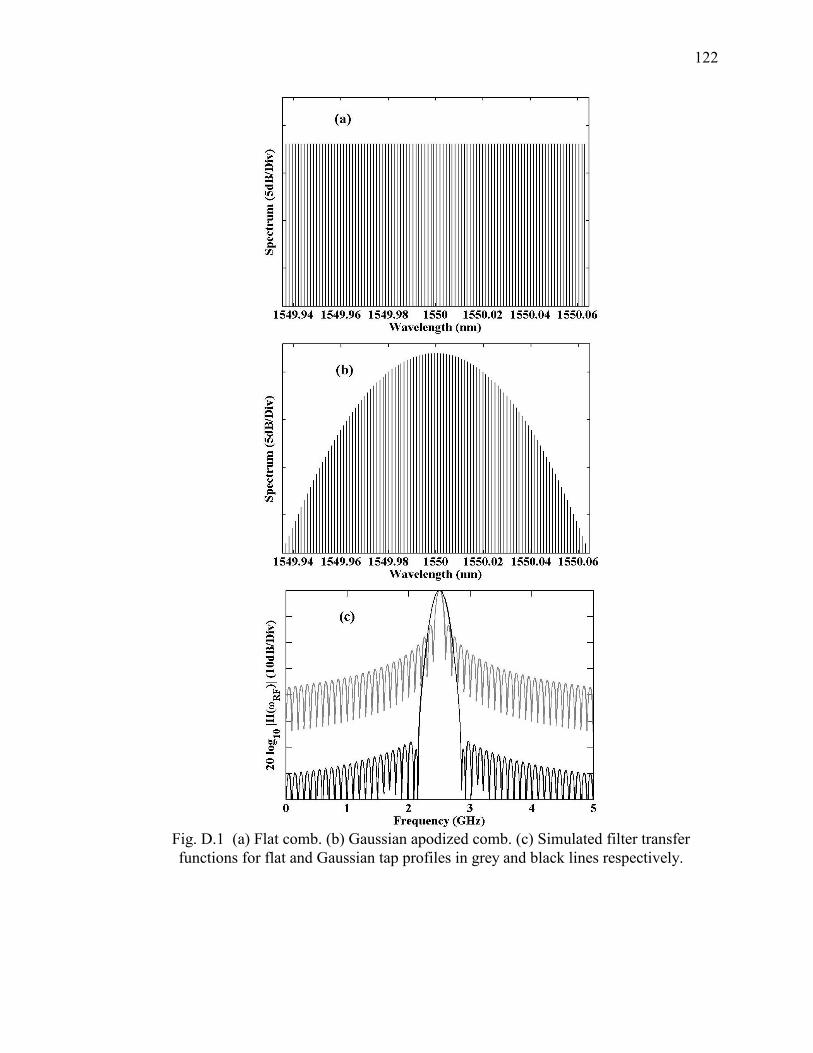
122
Fig. D.1 (a) Flat comb. (b) Gaussian apodized comb. (c) Simulated filter transfer
functions for flat and Gaussian tap profiles in grey and black lines respectively.

123
Now we simulate the 3-dB BW and SLS as a function of maxline-to-minline
extinction which we define it as the extinction between the strongest line to the weakest
line for a comb apodized with a Gaussian profile. The simulation results are shown in
Fig. D.2. As we notice by increasing the maxline-to-minline extinction in logarithmic
scale, the SLS increases linearly in logarithmic scale and the FWHM of filter passband
also increases linearly in linear scale.
Fig. D.2 SLS and 3-dB BW as a function of maxline-to-minline extinction of a Gaussian
apodized comb with 100 lines.
Depending on the application, different filter properties might be of interest. Here
we define suppression points at one and half times of the filter FWHM away from the
bandpass center. This property identifies the sharpness of the filter or in other words the
slope of the filter at the band edges.
Fig. D.3 SLS for >1.5FWHM away from the bandpass center and 3-dB BW as a function
of comb maxline-to-minline extinction.
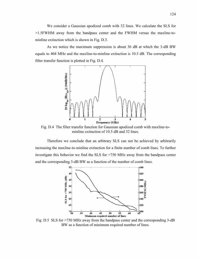
124
We consider a Gaussian apodized comb with 32 lines. We calculate the SLS for
>1.5FWHM away from the bandpass center and the FWHM versus the maxline-to-
minline extinction which is shown in Fig. D.3.
As we notice the maximum suppression is about 36 dB at which the 3-dB BW
equals to 404 MHz and the maxline-to-minline extinction is 10.5 dB. The corresponding
filter transfer function is plotted in Fig. D.4.
Fig. D.4 The filter transfer function for Gaussian apodized comb with maxline-to-
minline extinction of 10.5 dB and 32 lines.
Therefore we conclude that an arbitrary SLS can not be achieved by arbitrarily
increasing the maxline-to-minline extinction for a finite number of comb lines. To further
investigate this behavior we find the SLS for >750 MHz away from the bandpass center
and the corresponding 3-dB BW as a function of the number of comb lines.
Fig. D.5 SLS for >750 MHz away from the bandpass center and the corresponding 3-dB
BW as a function of minimum required number of lines.

125
Here we also assume the comb is Gaussian apodized; however, we set the
maxline-to-minline extinction such that we achieve the maximum SLS. The simulation
results are illustrated in Fig. D.5. We note that for 48 lines with a 21-dB maxline-to-
minline extinction we can achieve 60-dB suppression for >750 MHz away from the
bandpass center which has a corresponding 3-dB BW of 354 MHz.

VITA
126
VITA
Ehsan Hamidi received the B.Sc. degree in Electrical Engineering from Sharif
University of Technology, Tehran, Iran, in 2005, and is currently a Ph.D. candidate in the
School of Electrical and Computer Engineering at Purdue University, West Lafayette, IN.
He has been a Research Assistant in the Ultrafast Optics and Optical Fiber
Communications Laboratory since 2005. His current research interests include Radio
Frequency Photonics, Ultrafast Optics, Optical Pulse Shaping, and Optical Signal
Processing, Optical Frequency Combs, and Optical Metrology.
Mr. Hamidi is a student member of the IEEE Photonics Society and the IEEE
Communications Society. He was nominated as a student paper award finalist in 29th
International Union of Radio Science General Assembly, 2009 IEEE International
Symposium on Antennas and Propagation, and 2010 IEEE International Topical Meeting
on Microwave Photonics. He has served as a reviewer for IEEE/OSA Journal of
Lightwave Technology, IEEE Photonics Technology Letters, Optics Letters, and Optics
Express.