Subtask A: Final Report Presentation to ExCo June 14, 2013 - Task 43

HAWAII NATURAL ENERGY INSTITUTEwww.hnei.hawaii.eduDOE Hydrogen Program Review 2007, Arlington
Photoelectrochemical Hydrogen Production: UNLV-SHGR Program Subtask
This presentation does not contain any proprietary or confidential information
Robert PerretUniversity of Nevada Las Vegas
Research Foundation
Eric L. MillerUniversity of Hawaii at Manoa
15 May 2007 #PDP37

2
• Project start date: 1 Oct. 2004• Project end date: 31 Dec. 2007• Percent complete: 70%
• Barriers for photoelectrochemical(PEC) H2 production technologies:
–Y: Materials Efficiency–Z: Materials Durability–AB: Bulk Materials Synthesis–AC: Device Configuration Designs
• Total project funding: $2.81M–DOE share: $1,685,861–Contractor share: $1,123,361
• FY06 Funding : $ 958k• Funding for FY07: $0
Timeline
Budget
Barriers
• University of Hawaii at Manoa / Eric L. Miller• University of Nevada, Las Vegas / Clemens Heske• University of California, Santa Barbara /
Eric McFarland• National Renewable Energy Laboratory /
Mowafak Al-Jassim & John Turner• MVSystems Incorporated / Arun Madan• Intematix Corporation / Xiaodong Xiang• Altair Nanotechnologies Incorporated /
Vesco Manev
Collaborators / PIs
OVERVIEW

3
The primary objective is to assist DOE in the development of hydrogen-production technology utilizing solar energy to photoelectrochemically split water. The primary focus is on low-cost thin film materials (such as metal oxides) and novel multi-junction thin film devices (such as the UH-Hybrid Photoelectrode- HPE)
OBJECTIVES
Identify and develop new PEC film materials compatible with high-efficiency, low-cost H2 production devices: Target: 1.6 mA/cm2 – 6.5 mA/cm2 AM 1.5 photocurrentDemonstrate functional multi-junction device incorporating best-available PEC film materials: Target: 2 - 8 % STH efficiency under AM 1.5 illuminationDevelop avenues, integrating new theoretical, synthesis and analytical techniques, for optimizing future PEC materials and devicesExplore avenues toward manufacture scaled devices and systems
catalystFoil Substrate
Solid-state-junctionConductive Interface (e.g., ITO)
Photoactive PEC Film
light
HPE Deviceelectrolyte
DOE PEC Program Targets
Specific UNLV-SHRG PEC Project Goals
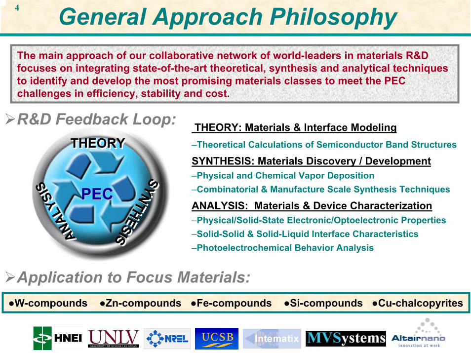
4 General Approach PhilosophyThe main approach of our collaborative network of world-leaders in materials R&D focuses on integrating state-of-the-art theoretical, synthesis and analytical techniques to identify and develop the most promising materials classes to meet the PEC challenges in efficiency, stability and cost.
THEORY: Materials & Interface Modeling–Theoretical Calculations of Semiconductor Band Structures
SYNTHESIS: Materials Discovery / Development–Physical and Chemical Vapor Deposition –Combinatorial & Manufacture Scale Synthesis Techniques
ANALYSIS: Materials & Device Characterization–Physical/Solid-State Electronic/Optoelectronic Properties–Solid-Solid & Solid-Liquid Interface Characteristics –Photoelectrochemical Behavior Analysis
THEORYTHEORY
SYNTHESIS
SYNTHESISANAL
YSIS
ANAL
YSIS PECPEC
R&D Feedback Loop:
Application to Focus Materials:
tu
●W-compounds ●Zn-compounds ●Fe-compounds ●Si-compounds ●Cu-chalcopyrites
5 SUMMARY
Collaborative Research Team Established: combining materials theory, synthesis and characterizations, to expedite the materials discovery and development process for improved PEC devices.Critical Experience, Protocols, and Infrastructure Developed:
–Versatile synthesis tools established for fabricating PEC materials & devices–Comprehensive characterization protocols established for PEC materials & devices– Rapid-throughput synthesis & screening techniques developed to facilitate discovery– Manufacture scale process demonstrated for HPE device fabrication
Focus Materials Classes Established: including WO3-, ZnO- Fe2O3-, silicon- , and copper chalcopyrite-based thin films.Key Targets Met in Focus Materials Experiments:
–Photocurrents in excess of 3 mA/cm2 in tungsten-based compound films–Photocurrents in excess of 6.5 mA/cm2 in Si- and chalcopyrite-based films (with additional bias
constraints to be corrected in band edge alignment modifications)–STH Device efficiencies in excess of 3% in WO3-based multijunction structures under 1 sun
FUTUREContinued Development of Research Team Capabilities and CollaborationContinued Optimization of Performance and Durability in Focus MaterialsContinued Discovery of New Materials and Possible Down-Selection of Old MaterialsSelection of Best Materials for Incorporation in High-Efficiency PEC Devices
PROGRESS

6 Approach: Theory
Background of Density-Functional Theory (DFT):
K-S equation)()()()(8
22
2
rrrVrm
hj
KSjjeffj ψεψψ
π=+∇−
)()()()( rVrVrVrV XCNHeff ++=
:)(rVXC Exchange-correlation potentials: LDA, or GGA
Applications:Total energies, Electronic structures such as band structure anddensity of states, Optical properties such as optical absorptioncoefficient and transition properties
To provide theoretical guidance and understanding on materials studied by the PEC teamTo search for new materials and new concepts
Theoretical modeling of PEC materials:

7 Approach: Theory
Collaboration on WO3with the PEC team:
Results on ZnO:N-incorporation leads to bandgap reduction in ZnOGa-N cluster doping may form intermediate band in ZnOGroup-IB elements (Cu, Ag, Au) lead to VBM up shift in ZnOp-type and gap reduced ZnO is possible by Cu and Ag incorporationGa-N cluster doping may form intermediate band in ZnO
Specific Applications in PEC Materials
Determined conduction and valence band positions for cation and anion doped WO3 –Nitrogen incorporation leads to bandgap reduction in WO3–Calculated optical absorption coefficient for WO3:N–Calculated a minimal shift for the conduction band minimum with molybdenum doping.
New Materials:Theoretical results from WO3 and ZnO to be included in modeling of new PEC
material systems

8 Approach: SynthesisCollectively, our team commands a broad portfolio of thin film synthesis techniques to facilitate the discovery and development of PEC materials and devices for high-performance, low-cost hydrogen production systems, including. Team synthesis capabilities include:
Physical Vapor Deposition SystemsChemical Vapor Deposition SystemsSpray Pyrolysis Fabrication SystemsSol-Gel Fabrication Systems
Reactive sputtering system for compound material films (including oxides, sulfides, etc.)
Co-Evaporation system for copper chalcopyrite films (CIGS, CGS, etc.)
Plasma-enhanced CVD system for low temperature synthesis of metal oxide films
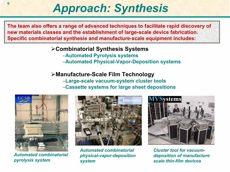
9 Approach: SynthesisThe team also offers a range of advanced techniques to facilitate rapid discovery of new materials classes and the establishment of large-scale device fabrication. Specific combinatorial synthesis and manufacture-scale equipment includes:
Combinatorial Synthesis Systems–Automated Pyrolysis systems–Automated Physical-Vapor-Deposition systems
Manufacture-Scale Film Technology–Large-scale vacuum-system cluster tools–Cassette systems for large sheet depositions
Automated combinatorial pyrolysis system
Automated combinatorial physical-vapor-deposition system
Cluster tool for vacuum-deposition of manufacture scale thin-film devices
10 Approach: Characterizations
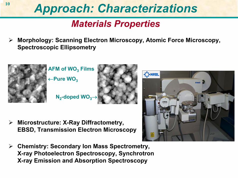
Morphology: Scanning Electron Microscopy, Atomic Force Microscopy, Spectroscopic Ellipsometry
Microstructure: X-Ray Diffractometry,EBSD, Transmission Electron Microscopy
Chemistry: Secondary Ion Mass Spectrometry,X-ray Photoelectron Spectroscopy, SynchrotronX-ray Emission and Absorption Spectroscopy
AFM of WO3 Films
←Pure WO3
N2-doped WO3→
Materials Properties
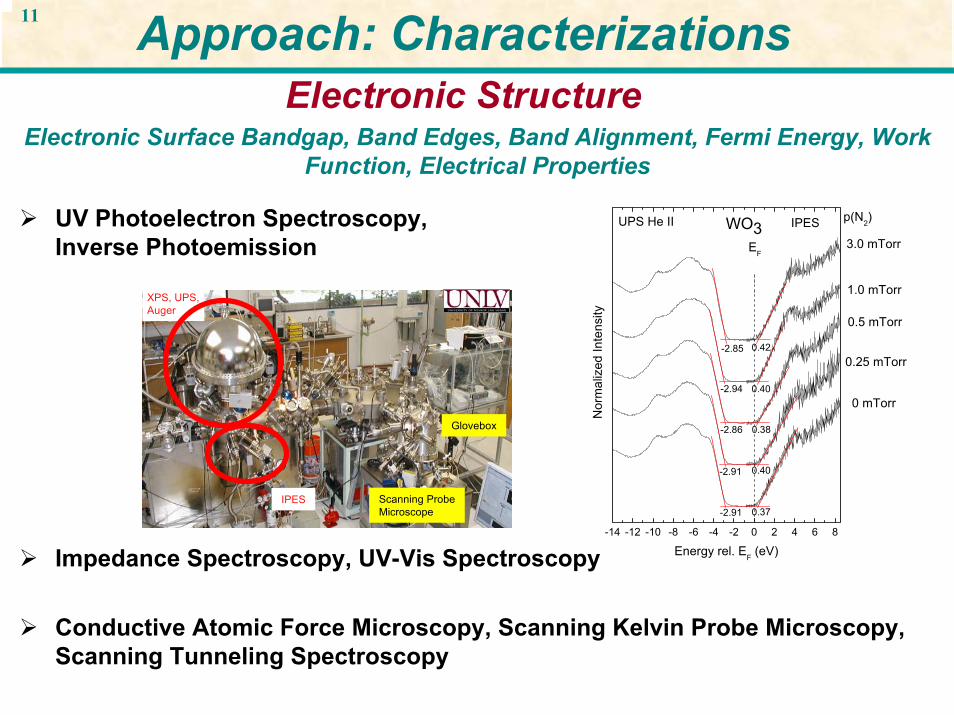
11 Approach: CharacterizationsElectronic Structure
Electronic Surface Bandgap, Band Edges, Band Alignment, Fermi Energy, Work Function, Electrical Properties
UV Photoelectron Spectroscopy,Inverse Photoemission
Impedance Spectroscopy, UV-Vis Spectroscopy
Conductive Atomic Force Microscopy, Scanning Kelvin Probe Microscopy, Scanning Tunneling Spectroscopy
Scanning ProbeMicroscope
IPES
XPS, UPS,Auger
Glovebox
-14 -12 -10 -8 -6 -4 -2 0 2 4 6 8
WO3
0.42-2.85
-2.94
0.38-2.86
0.40
0.37
3.0 mTorr
1.0 mTorr
0.5 mTorr
0.25 mTorr
0 mTorr
IPES
Nor
mal
ized
Inte
nsity
Energy rel. EF (eV)
UPS He II
EF
p(N2)
-2.91
-2.91
0.40
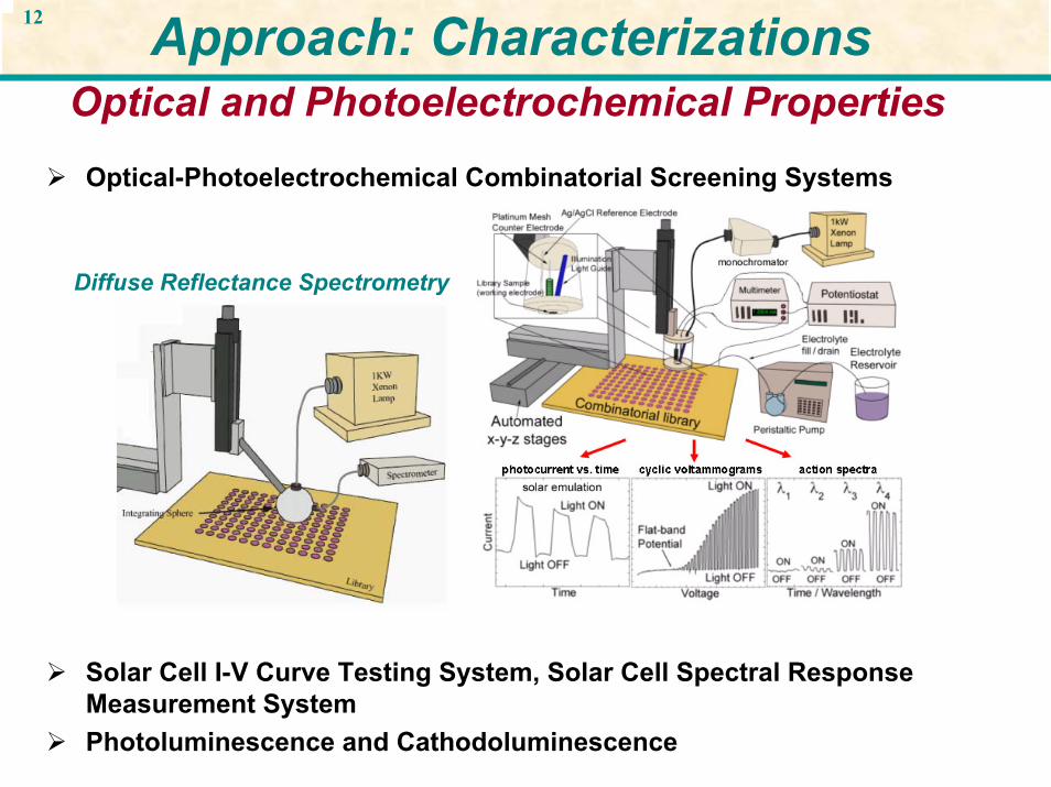
12 Approach: CharacterizationsOptical and Photoelectrochemical Properties
Optical-Photoelectrochemical Combinatorial Screening Systems
Solar Cell I-V Curve Testing System, Solar Cell Spectral Response Measurement SystemPhotoluminescence and Cathodoluminescence
Diffuse Reflectance Spectrometry

13
Our team utilizes its collective expertise and capabilities in theoretical materials modeling, in materials synthesis, and in materials screening and characterization to identify and develop an expansive set of promising PEC thin-film materials classes. The five classes of “focus materials” currently under investigation include:
Tungsten-Based Compound Films (U. Hawaii, Intematix)–Modified Tungsten Oxide Compounds with Anion/Cation Substitutions
Zinc-Based Compound Films (NREL)–Modified Zinc Oxide Compounds with Anion/Cation Substitutions
Iron-Based Compound Films (UCSB, Altair Nano)–Novel Iron-Based Compound Materials, including Fe2O3 Nanorods
Silicon-Based Compound Films (MVSystems)–Amorphous Silicon Carbide Films with p- and n- type Doping
Copper Chalcopyrite Compound Films (U. Hawaii)–Copper-Indium-Gallium-Selenium-Sulfur Compounds
Specific Approach: Focus Materials

14 Progress: Tungsten-Based Compound Films
Hybrid Photoelectrode with pure WO3 films
0
2
4
6
8
10
0.0 0.5 1.0 1.5 2.00
2
4
6
8
10
12
Integrated HPE performance level
a-Si/a-Si tandem, filtered by WO3 film
a-Si/a-Si tandemstainless steel substrate
High performance WO3 film
Cur
rent
(mA
/cm
2 )
Voltage (V)
STH
efficiency (%)
0
2
4
6
8
10
0.0 0.5 1.0 1.5 2.00
2
4
6
8
10
12
Integrated HPE performance level
a-Si/a-Si tandem, filtered by WO3 film
a-Si/a-Si tandemstainless steel substrate
High performance WO3 film
Cur
rent
(mA
/cm
2 )
Voltage (V)
STH
efficiency (%)
Glass substrate
Glass substrate
Non-Conductive Epoxy
WO3
RTV SiliconeITOa-Si
(nip-nip) TCO
TCO
Glass substrate
Glass substrate
Non-Conductive Epoxy
WO3
RTV SiliconeITOa-Si
(nip-nip) TCO
TCO
00.0
0.5
1.0
1.5
2.0
2.5
3.0
20 40 60 80 100C
urre
nt (m
A/c
m2 )
Load Line Analysis Device Configuration time (min)
Performance
Tungsten oxide is a model material to study PEC hydrogen generation…
Sufficient absorption to generatemodest photocurrents
Good electron transport properties
High Stability in Electrolytes
Thin film process scalable
Demonstrated in prototype multi-junction devices.
promiseNon ideal band edge alignment –requires supplemental bias
Bandgap requires reduction to increase photocurrents
The photostability over extended time periods and for new tungsten-alloy compositions requires validation
challenges

15 Progress: Tungsten-Based Compound Films
1.6 1.8 2.0 2.2 2.4 2.6 2.8 3.00
50
100
150
200
250
0 mTorr N2 2 mTorr N2 3 mTorr N2 4 mTorr N2 6 mTOrr N2
hν (eV)
(αhν
)1/2 (c
m-1ev
)1/2
UV edge plotted as indirect bandgapCalculated current density based on UV absorption edge for a 1 μm thick filmShaded region represents absorbed portion of AM1.5G
Pure WO3 – 2.59 mA/cm2
4 mTorr N2 – 6.30 mA/cm2
With sufficient nitrogen in the sputtering ambient, bandgap reductions are realized, however this increase in absorption does not correlate with an increase in measured photocurrents . . .
0.0 0.4 0.8 1.2 1.6 2.0 2.40.0
0.5
1.0
1.5
2.0
2.5
3.0
3.5 0 mTorr N2 2 mTorr N2 3 mTorr N2 4 mtorr N2 6 mTorr N2
Cur
rent
Den
sity
(mA
/cm
2 )
Potential (V vs. SCE)
0.33 M H3PO4AM 1.5G illumination
PEC testing of WO3:N

16
2 0 2 1 2 2 2 3 2 4 2 5 2 6 2 7 2 8 2 9 3 0
6 m T o r r N 2 4 m T o r r N 2 3 m T o r r N 2 2 m T o r r N 2 0 m T o r r N 2
D e g re e s (2 - th e ta )
Cou
nts
(nor
mal
ized
)
2 0 2 1 2 2 2 3 2 4 2 5 2 6 2 7 2 8 2 9 3 0
6 m T o r r N 2 4 m T o r r N 2 3 m T o r r N 2 2 m T o r r N 2 0 m T o r r N 2
D e g re e s (2 - th e ta )
Cou
nts
(nor
mal
ized
)Influence of Nitrogen on Structure
X-ray diffraction pattern shows an initial decrease in crystallinity for monoclinic phase followed by transformation to a stabilized cubic phase for nitrogen partial pressures greater than 3mTorr. The TEM diffraction pattern for nitrogen doping shows smearing, indicating a highly defective lattice.
Progress: Tungsten-Based Compound Films
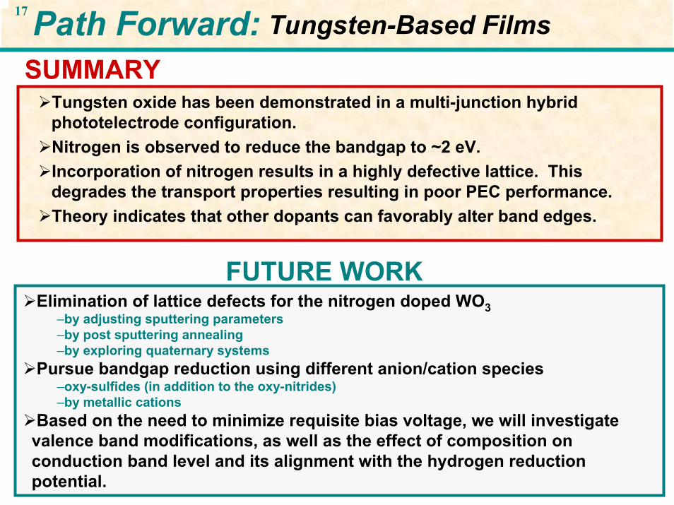
17Tungsten-Based FilmsPath Forward:
Elimination of lattice defects for the nitrogen doped WO3–by adjusting sputtering parameters–by post sputtering annealing–by exploring quaternary systems
Pursue bandgap reduction using different anion/cation species–oxy-sulfides (in addition to the oxy-nitrides)–by metallic cations
Based on the need to minimize requisite bias voltage, we will investigate valence band modifications, as well as the effect of composition on conduction band level and its alignment with the hydrogen reduction potential.
SUMMARY
FUTURE WORK
Tungsten oxide has been demonstrated in a multi-junction hybrid phototelectrode configuration.Nitrogen is observed to reduce the bandgap to ~2 eV.Incorporation of nitrogen results in a highly defective lattice. This degrades the transport properties resulting in poor PEC performance.Theory indicates that other dopants can favorably alter band edges.

18 Progress: Zinc-Based Compound FilmsZnO is inexpensive, nontoxic, and easy to synthesize. It also has adirect bandgap and high electron mobility thereby making it a good candidate for PEC splitting of water.
Conduction band edge only slightly mismatched to drive the hydrogen reaction.
Impurity doping can shift the valence band edge, providing for bandgap reduction.
Can also fabricate as P-type ZnO
promiseBandgap is too large to effectively utilize the visible light
Requires stability improvement against photocorrosion
challenges
• Impurity doping using anion or cation species
Bandgap reduction Explore p-type ZnO• Impurity doping using group 1B
metals
strategies for PEC improvement

19 Progress: Zinc-Based Compound FilmsStructural evolution for RF sputtering of ZnO:N
High quality pure ZnO thin films are synthesizedN-incorporation into ZnO thin films was achievedBandgap reduction in ZnO thin films was achieved by N-incorporationPhoto-response in ZnO:N thin films was demonstrated
400 500 600 700 800 900 1000 1100 12000.0
0.1
0.2
0.3
0.4
0.5
0.6
0.7
0.8
0.9
1.0 ZnO ZnO:N at 80 W ZnO:N at 100 W ZnO:N at 120 W ZnO:N at 150 W ZnO:N at 200 W Zn3N2
Wavelength (nm)
Abs
orba
nce
Optical absorption spectra from ZnO:N samples
-0.6 -0.4 -0.2 0.0 0.2 0.4 0.6 0.8 1.0 1.2
0
10
20
(c) As-grown ZnO Annealed ZnO ZnO:N
Light power: 75 mW/cm2
Phot
ocur
rent
(μA
cm-2
)
Potential (V vs. Ag/AgCl)
200 400 600 800 10000
50
100
Tra
nsm
ittan
ce (%
T)
Wavelength (nm)
UV/IR filter Red filter
Photocurrent-voltage curves of the samples under light illumination with the UV/IR filter
Solution: Na2SO4
pH: 6.8
30 35 40 45 50 55
* *
*
ZnO(101)
Zn3N2
(440)Zn3N2
(400)
Zn3N2
ZnO:N at 200 W
ZnO:N at 150 WZnO:N at 120 W
ZnO:N at 100 W
ZnO:N at 80 W
ZnO
Inte
nsity
(a.u
.)
2θ (degree)
Substate
ZnO(002)
*
30 35 40 45 50 55
* *
*
ZnO(101)
Zn3N2
(440)Zn3N2
(400)
Zn3N2
ZnO:N at 200 W
ZnO:N at 150 WZnO:N at 120 W
ZnO:N at 100 W
ZnO:N at 80 W
ZnO
Inte
nsity
(a.u
.)
2θ (degree)
Substate
ZnO(002)
*

20
Bandgap reduction in ZnO thin films was achieved by Cu-incorporationP-type ZnO thin films with reduced bandgaps were achieved by Cu incorporationPhoto-response in ZnO:Cu thin films was demonstrated
400 500 600 700 800 900 10000.00.10.20.30.40.50.60.70.80.91.01.11.2
ZnO ZnO:Cu(4) ZnO:Cu(6) ZnO:Cu(10) ZnO:Cu(12)
Wavelength (nm)
Abs
orba
nce
(b)
Optical absorption spectra from ZnO:Cu samples Photocurrent-voltage curves of p-type ZnO:Cu samples
-0.6 -0.4 -0.2 0.0 0.2 0.4 0.6
-300
-250
-200
-150
-100
-50
0
50
Photo currents Undoped ZnO ZnO:Cu(4) ZnO:Cu(6) ZnO:Cu(10) ZnO:Cu(12)
Phot
ocur
rent
(μA
cm-2)
Potential (V vs. Ag/AgCl)
Solution: Na2SO4
pH: 6.8
Cu increase Grain size and surface roughness decreased
Progress: Zinc-Based Compound Films

21Zinc-Based Compound FilmsPath Forward:
SUMMARY
FUTURE WORK
Preliminary work shows that nitrogen can be effectively incorporated into ZnO films to reduce bandgapNeed to improve crystallinity for ZnO:N to realize good PEC properties.Theoretical calculations show that doping with group 1B transition metals (Cu, Ag) results in bandgap reduction.Cu was incorporated into ZnO films with mixed results – bandgapreduction is observed and Cu is found at Zn sites for select films, however the measured photocurrents are low.
The process for RF sputtering of ZnO films requires optimization.–Study the film growth as a function of substrate temperature.–Incorporation of impurity dopants via co-sputtering will be employed.
Band gap reduction–Impurity band generation by new impurities–Acceptor-donor co-doping
Stability improvement

22 Progress: Iron-Based Compound Films
strategies for PEC improvement
• Growth of crystalline oxide• Direct growth along the preferred
electron conduction paths• High Surface Area Materials
Photon To Electron Conversion Increase
Shift of Bandpositions
•Quantum size effects•Transition metal doping
Improve Kinetics of Water Oxidation
• Identify and deposit optimized surface oxidation electro-catalyst
Bandgap ~ 2 eV (40% solar light absorption).Abundant and inexpensiveHigh Stability in Electrolytes (pH>3)
Carrier TransportValence Band EdgeWater Oxidation Kinetics
Low optical absorption
challenges
Iron Oxide, as a commonly-found material with bandgap well-suited for the direct solar water splitting of water, is considered the “Holy Grail” of PEC materials- but its performance has been severely limited by opto-electronic properties…
promise

23 Progress: Iron-Based Compound FilmsSynthesis of nanorod electrodes
Synthetic control of nanorod structure
1) 35 ± 3 nm 2) 21 ± 2 nm 3) 20 ± 3 nm 4) 12 ± 3 nm
SubstrateFeCl3+Salt Quartzsubstrate
Ti/Pt
β-FeOOH
α-Fe2O3
nanorods
Thermaltreatment
RuO2
Electrocatalystdeposition

24
360 400 440 480 520 560 600 640 680
0
2
4
6
8
10
12
14
16
18
20S116C
RuO2 No Catalyst Cobalt
0.1M NaOH 400mV appliedbias vs Ag/AgCl N2 Purged
IPC
E (%
)
Wavelength (nm)360 400 440 480 520 560 600 640 680
0
2
4
6
8
10
12
14
16
18
20
IPC
E (%
)
Wavelength (nm)
S116C RuO2
No Catalyst Cobalt
0.1M NaOH 100mV appliedbias vs Ag/AgCl N2 Purged
Applied BiasApplied Bias
100 mV100 mV 400 mV400 mV
No CatalystNo Catalyst 0.3%0.3% 1.0%1.0%
RuORuO22 1.6%1.6% 0.9%0.9%
CobaltCobalt 0.2%0.2% 1.0%1.0%* Efficiency from IPCE data
1) 2) 3)
1) Photoelectrochemical performance of 21 and 15 nm nanorods under applied bias showingand efficiency of 1.3% and 1% respectively. (2,3) IPCE of 35nm Fe2O3 nanorods with an applied bias of 100mV and 400mV, graph 2 and 3 respectively, showing the dramatic improvement of the nanorods with the electrodeposition of RuO2 at low applied bias while at high applied bias the oxygen evolution catalyst is not improving the performance of the nanorods. 4) Table of results showing the Efficiency of the nanorods from graph 2 and 3.
4)
20 30 40 50 60
S
SS
S
Cou
nts
(a.u
.)
2 θ (deg.)
Hematite Nanorods (0.5M NaNO3) Hematite Nanorods (1M NaNO3)
H-(012)H-(104)
H-(110)
H-(113)
H-(024)H-(300)
S S-SubstrateH-Hematite
50 nm
Nanorod characterization & performanceProgress: Iron-Based Compound Films

25 Path Forward: Iron-Based Compound Films
SUMMARYEarly stages of research and development on iron oxide nanorods synthesis have shown:
Control over the size and morphology of the nanostructuresImproved photoelectrochemical performance as compared with spray
pyrolysis deposited filmsPhotoelectrochemical efficiencies of ~1 %
This synthesis method is applicable to wide variety of substrates and can be adapted to any size of substrates.
Control gross structure of photocatalysts– Nanorod synthesis conditions (pH, T, electrolyte composition)– Explore use of framework templates (deposit in cubic phase nanopores)
Control opto-electronic properties– Nanorod size reduction to increase VB Confinement at d<6nm– Nanorod growth to be along (110) plane– Nanorod doping by in situ growth or high temperature diffusion
Control kinetics– Selective deposition of surface electrocatalysts (start with Pt, Ni, Au, Ru)
FUTURE WORK

26 Progress: Silicon-Based Compound FilmsAmorphous silicon carbide is an electrochemically stable and photoactive material with tunable bandgap, which would enable the fabrication of “all-silicon” multi-junction water-splitting devices.
Tunable bandgap of 2.0-2.3 eVand good optoelectronic qualityLarge knowledgebase from a-Si technologya-SiC shows good corrosion resistanceEnables “all-silicon multi-junction device” to be fabricated in a “cluster tool” machine
Non-ideal band edge alignment –requires supplemental bias
Kinetic limitations apparent for bare a-SiC electrodesLong term corrosion and photo-corrosion behavior is not known
promise challenges
1.7
1.9
2.1
2.3
2.5
0.0 0.1 0.2 0.3 0.4 0.5 0.6CH4/(CH4+SiH4) in source gases
Tauc
Eg
(eV
) Amorphous SiPanel
Bandgaptuning by carbon content(Gas flow ratio)

27 Progress: Silicon-Based Compound FilmsAll-Silicon Hybrid PEC Device Designs
n i p n i p
a-S
iCEg
2-2.
3eV
a-Si
Eg=1
.75e
V
nc-S
iEg
~1.1
eV
Sta
inle
ss S
teel
Su
bstra
te
O2C
atal
yst
photon 1photon 2
photon 3
qV1
qV2
qV3
elec
troly
te
elec
troly
te
photons
photons
(HER)
(OER)
h+
e-
* US patent #6,258,408B1: MVSystemslarge-scale cluster tool design reel-to-reel cassette*
light
H2 evolutionPhotoactivep-type a-SiC layer
ohmic interface
a-Si and/or nc-Si solar cell
Stainless steel substrate O2 evolution catalyst
O2 evolution
electrolyte
Cluster-tool fabrication equipment
Device schematic Band diagram using A-Sic PEC film

28
0
20
40
60
80
100
300 500 700 900 1100Wavelength (nm)
Opt
ical
Tra
nsm
issi
on (%
)
a-SiC Eg=2.0eV, 0.20 um
a-SiC Eg=2.0eV, 0.31 um
-15
-12
-9
-6
-3
0
-1.4 -1.2 -1.0 -0.8 -0.6Potential (V vs SCE)
Cur
rent
(mA
/cm
2 )
Progress: Silicon-Based Compound Films
Photocurrent of >9mA/cm2
with a-SiC photocathode
Route to >10% STH Efficiency
photo-electrode
photo-electrode bandgap
(eV)
current available (m A/cm 2)
photovoltaic layer
configuration
current available
(filtered by top layer) (m A/cm 2)
possible STH (% )
achieved STH to date(% )
W O 3 2.6-2.8 4.3-3.3 a-S i/a-S i 8.0 5.3 3.1SiC 2 14.4 a-S i/nc-S i 6.0 7.4SiC 2.35 8.1 a-S i/nc-S i 7.8 ~10SiC ~2 ~14 nc-Si ~14 ~17
1-sunAM1.5 G
0.33M H3PO4
a-SiC EG=2.0eV, 0.31 um
Optical properties tailored through bandgap and thickness

29Silicon-Based Compound FilmsPath Forward:
SUMMARY
FUTURE WORK
One-sun photocurrent of ~9 mA/cm2 demonstrated for a-SiC electrodea-SiC films appear stable in cathodic regime (short-term tests)Flatband potential and photocurrent onset indicate non-ideal valence band maximum position and kinetic limitationsa-SiC is compatible with automated fabrication of multijunction devices in cluster tool deposition machine
Optimize optoelectronic quality of a-SiC at EG=2.0eV-2.3eV– systematic variation of PECVD process parameters
Comprehensive PEC characterization a-SiC photoelectrodes– band positions, electrode kinetics– long term stability
Fabricate and characterize complete monolithic a-SiC/a-Si multijunctionPEC device
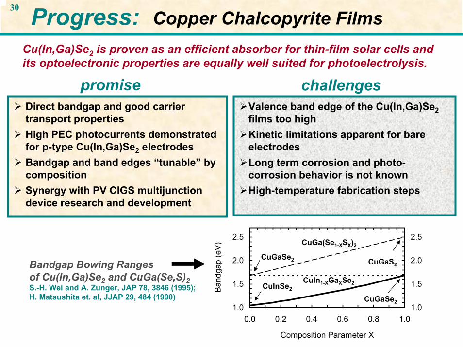
30 Progress: Copper Chalcopyrite Films
Direct bandgap and good carrier transport propertiesHigh PEC photocurrents demonstrated for p-type Cu(In,Ga)Se2 electrodesBandgap and band edges “tunable” by composition Synergy with PV CIGS multijunctiondevice research and development
Valence band edge of the Cu(In,Ga)Se2films too highKinetic limitations apparent for bare electrodesLong term corrosion and photo-corrosion behavior is not knownHigh-temperature fabrication steps
Bandgap Bowing Rangesof Cu(In,Ga)Se2 and CuGa(Se,S)2S.-H. Wei and A. Zunger, JAP 78, 3846 (1995);H. Matsushita et. al, JJAP 29, 484 (1990)
promise challenges
Cu(In,Ga)Se2 is proven as an efficient absorber for thin-film solar cells and its optoelectronic properties are equally well suited for photoelectrolysis.
1.0
1.5
2.0
2.5
0.0 0.2 0.4 0.6 0.8 1.0
Composition Parameter X
Band
gap
(eV)
1.0
1.5
2.0
2.5CuGa(Se1-XSX)2
CuIn1-XGaXSe2
CuGaSe2
CuInSe2
CuGaS2
CuGaSe2

31 Progress: Copper Chalcopyrite Films
Electrodes are stable during short-term PEC testingValence band edge too positive in current samples – high bias requiredPhotocurrent onset at least 0.3V more cathodic than flatband potentialResistance of back contact (high/SnO2:F vs low/Mo) has strong impact on photocurrent curve
before before
after after
2μm
CuIn0.2Ga0.8Se2(3-stage process)
CuGaSe2(3-stage)
Stability: morphology before/after PEC testing
0
200
400
600
800
1000
1200
-2.0 -1.5 -1.0 -0.5 0.0Potential (V vs SCE)
J2 (mA
2 /cm
4 )
CIGS/Mo
CIGS/SnO2
3-stage CGS/SnO2
2-stage CGS/SnO2
Photocurrent onset potential
CIGS/Mo:Illuminated open-circuit
=0.07 V vs SCE=0.31 V vs NHE
Stability, and Band Edge Positions

32
25 30 35 40 45 50 55
2 Theta (degrees)
log(
Inte
nsity
)Progress: Copper Chalcopyrite Films
-40
-30
-20
-10
0
-1.0 -0.8 -0.6 -0.4 -0.2 0.0Potential (V vs SCE)
Cur
rent
(mA
/cm
2 )
-40
-30
-20
-10
0
-0.4 -0.2 0.0 0.2 0.4 0.6 0.8Bias Voltage (V)
Cur
rent
(mA
/cm
2 )
28.3 mA/cm2 28.0 mA/cm2
VOC=663mVFF=0.613η=11.3%
in 0.5M H2SO4
CuIn1-xGaxSe2
Mo back contact
Soda-lime glass
light
CdS
CuIn1-xGaxSe2
ITO
Soda-lime glass
i-ZnO
light
Mo back contact
PEC electrode Solar cell1-Sun Photocurrent: similar in PEC and PV Devices (CuIn0.4Ga0.6Se2)
CuGaSe23-stage process
SnO2
(112)
(220) (204)
(312)(116)
CuGaSe22-stage process
-40
-30
-20
-10
0
-2.0 -1.5 -1.0 -0.5 0.0Potential (V vs SCE)
Cur
rent
(mA
/cm
2 )CuGaSe2 deposition conditions, film texture, and photocurrent curves
Preliminary data shows possible effect of texture [(112)/(220)+(204)] on saturation photocurrent and dark current.
in 0.5M H2SO4
AM1.5G
XRD: CGS samples from 2 different recipes Photocurrent 1-sun AM1.5G
3-stage
2-stage
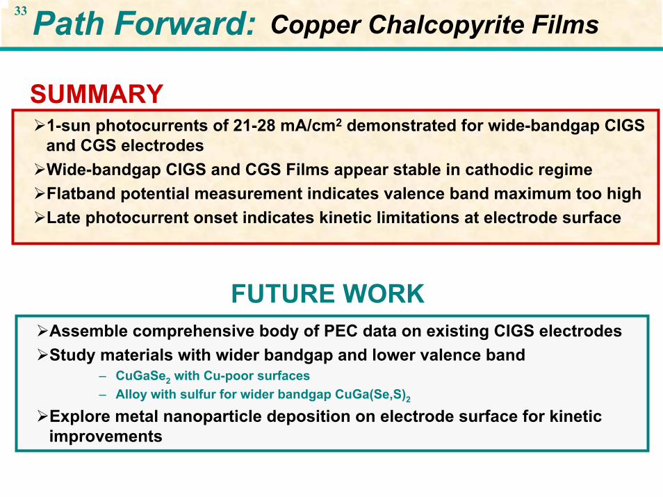
33Copper Chalcopyrite Films
SUMMARY
FUTURE WORK
Path Forward:
1-sun photocurrents of 21-28 mA/cm2 demonstrated for wide-bandgap CIGS and CGS electrodesWide-bandgap CIGS and CGS Films appear stable in cathodic regimeFlatband potential measurement indicates valence band maximum too highLate photocurrent onset indicates kinetic limitations at electrode surface
Assemble comprehensive body of PEC data on existing CIGS electrodesStudy materials with wider bandgap and lower valence band
– CuGaSe2 with Cu-poor surfaces– Alloy with sulfur for wider bandgap CuGa(Se,S)2
Explore metal nanoparticle deposition on electrode surface for kinetic improvements