Phos Palladium for Gold Wire Bonding to an … · Uyemura has brought advanced vacuum plasma...
4
UIC’s fiscal year just concluded. What it revealed was record sales, and our indisputable position as the industry’s #1 supplier of ENIG, ENEPIG, electroless gold, and via fill coppers. We are grounded in the idea that developing and adapting technologies that produce a substantial competitive advantage for our customers is our most important mission. At the core of this, always, is a commitment to scientific review, and what is provable. It is our highest endeavor to continue to bring to the market products that make customers successful - based on good science and good economics – and supported by the industry’s finest team of field professionals. Phos Palladium: The Better Choice for Gold Wire Bonding to an ENEPIG Finish Successful gold wire bonding is achieved between a gold wire and a clean soft gold surface finish. The wire has to be high purity (99.99+%); the mating surface must have a similar level of purity. Immersion gold deposits meet the purity requirement for gold wire bonding. Does it follow that ENIG is a good gold wire bondable surface finish? The short answer is no. The immersion gold in ENIG is crystalline in structure and as such, is susceptible to the diffusion of the underlying nickel to the surface. A nickel-contaminated gold surface will not successfully bond with the gold wire. (continued on pg. 2)
Transcript of Phos Palladium for Gold Wire Bonding to an … · Uyemura has brought advanced vacuum plasma...
UIC’s fiscal year just concluded. What it revealed was record sales, and our indisputable position as the industry’s #1 supplier of ENIG, ENEPIG, electroless gold, and via fill coppers.
We are grounded in the idea that developing and adapting technologies that produce a substantial competitive advantage for our customers is our most important mission. At the core of this, always, is a commitment to scientific review, and what is provable.
It is our highest endeavor to continue to bring to the market products that make customers successful - based on good science and good economics – and supported by the industry’s finest teamof field professionals.
Phos Palladium: The BetterChoice for Gold Wire Bondingto an ENEPIG FinishSuccessful gold wire bonding is achieved between a gold wire and a clean soft gold surface finish. The wire has to be high purity (99.99+%); the mating surface must have a similar level of purity.
Immersion gold deposits meet the purity requirement for gold wire bonding. Does it follow that ENIG is a good gold wire bondable surface finish? The short answer is no. The immersion gold in ENIG is crystalline in structure and as such, is susceptible to the diffusion of the underlying nickel to the surface. A nickel-contaminated gold surface will not successfully bond with the gold wire.(continued on pg. 2)
(continued)
ENIG Wire Bonding
Phos Palladium: The Better Choice forGold Wire Bonding to an ENEPIG Finish (continued )
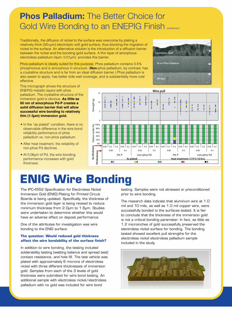
This micrograph shows the structure of ENEPIG metallic layers with phos palladium. The crystalline structure of the immersion gold is obvious. As little as 60 nm of amorphous Pd-P creates a solid diffusion barrier that will allow successful wire bonding to relatively thin (1-3µm) immersion gold.
The IPC-4552 Specification for Electroless Nickel Immersion Gold (ENIG) Plating for Printed Circuit Boards is being updated. Specifically, the thickness of the immersion gold layer is being revised to reduce minimum thickness from 2.0µm to 1.6µm. Studies were undertaken to determine whether this would have an adverse effect on deposit performance.
One of the attributes for investigation was wire bonding to the ENIG surface.
The question: Would reduced gold thickness affect the wire bondability of the surface finish?
In addition to wire bonding, the testing included solderability testing (wetting balance and spread test) contact resistance, and hole fill. The test vehicle was plated with approximately 6 microns of electroless nickel with three different thicknesses of immersion gold. Samples from each of the 3 levels of gold thickness were submitted for wire bond testing. An additional sample with electroless nickel/electroless palladium with no gold was included for wire bond
• In the “as plated” condition, there is no observable difference in the wire bond reliability performance of phos palladium vs. non-phos palladium.
• After heat treatment, the reliability of non-phos Pd declines.
• At 0.06µm of Pd, the wire bonding performance increases with gold thickness.
testing. Samples were not stressed or preconditioned prior to wire bonding.
The research data indicate that aluminum wire at 1.0 mil and 10 mils, as well as 1.0 mil copper wire, were successfully bonded to the surfaces tested. It is fair to conclude that the thickness of the immersion gold is not a critical bonding parameter. In fact, as little as 1.2 microinches of gold successfully preserved the electroless nickel surface for bonding. The bonding tested showed excellent pull strengths for the electroless nickel electroless palladium sample included in the study.
Immersion Gold
60 nm Phos Palladium
EN layer
Traditionally, the diffusion of nickel to the surface was overcome by plating a relatively thick (50+µm) electrolytic soft gold surface, thus blocking the migration of nickel to the surface. An alternative solution is the introduction of a diffusion barrier between the nickel and the bonding gold surface. A thin layer of amorphous electroless palladium (4µm; 0.01µm) provides this barrier.
Phos palladium is ideally suited for this purpose. Phos palladium contains 3-5% phosphorous and is amorphous in structure. (Non-phos palladium, by contrast, has a crystalline structure and is far from an ideal diffusion barrier.) Phos palladium is also easier to apply, has better side wall coverage, and is substantially more cost effective.
As electronic devices have miniaturized, so have their chip size packages, along with the spacing of wiring lines. As a result, short circuit risk has increased. Uyemura EPIG is an excellent response to this. Along with lowering the risk of short circuits, the plating process can be shortened, and EPIG may also be usable in high frequency devices.
Tests compared the characteristics of EPIG deposits with ENEPIG deposits. The ability to plate fine patterns, the solder joint reliability, and the wire bonding reliability of the electroless Pd/Au (EPIG) deposit process were compared with the electroless Ni-P/Pd/Au (ENEPIG) deposit process. The coupons used in this study consisted of a copper-clad laminated substrate plated to a thickness of 20µm using an acid copper electroplating process. Substrates were plated with Uyemura EPIG and ENEPIG.
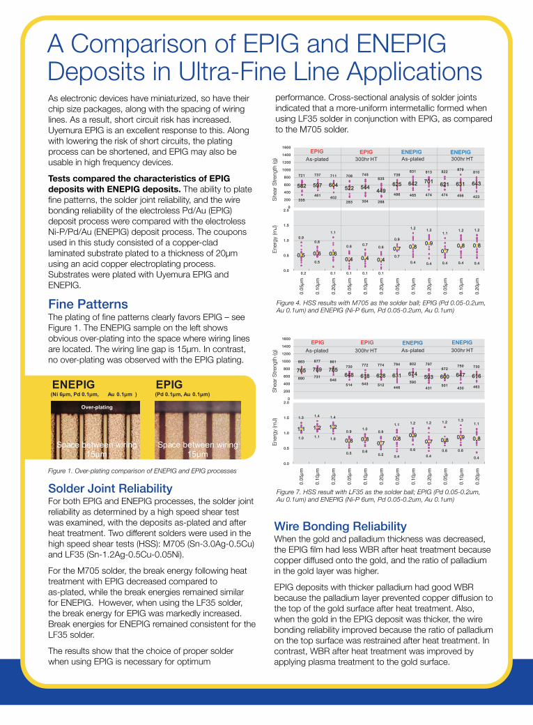
Fine PatternsThe plating of fine patterns clearly favors EPIG – see Figure 1. The ENEPIG sample on the left shows obvious over-plating into the space where wiring lines are located. The wiring line gap is 15μm. In contrast, no over-plating was observed with the EPIG plating.
Figure 1. Over-plating comparison of ENEPIG and EPIG processes
Solder Joint ReliabilityFor both EPIG and ENEPIG processes, the solder joint reliability as determined by a high speed shear test was examined, with the deposits as-plated and after heat treatment. Two different solders were used in the high speed shear tests (HSS): M705 (Sn-3.0Ag-0.5Cu) and LF35 (Sn-1.2Ag-0.5Cu-0.05Ni).
For the M705 solder, the break energy following heat treatment with EPIG decreased compared to as-plated, while the break energies remained similar for ENEPIG. However, when using the LF35 solder, the break energy for EPIG was markedly increased. Break energies for ENEPIG remained consistent for the LF35 solder.
The results show that the choice of proper solder when using EPIG is necessary for optimum
A Comparison of EPIG and ENEPIG Deposits in Ultra-Fine Line Applications
ENEPIG(Ni 6µm, Pd 0.1µm, Au 0.1µm )
EPIG(Pd 0.1µm, Au 0.1µm)
Space between wiring15µm
Space between wiring15µm
Over-plating
performance. Cross-sectional analysis of solder joints indicated that a more-uniform intermetallic formed when using LF35 solder in conjunction with EPIG, as compared to the M705 solder.
Wire Bonding ReliabilityWhen the gold and palladium thickness was decreased, the EPIG film had less WBR after heat treatment because copper diffused onto the gold, and the ratio of palladium in the gold layer was higher.
EPIG deposits with thicker palladium had good WBR because the palladium layer prevented copper diffusion to the top of the gold surface after heat treatment. Also, when the gold in the EPIG deposit was thicker, the wire bonding reliability improved because the ratio of palladium on the top surface was restrained after heat treatment. In contrast, WBR after heat treatment was improved by applying plasma treatment to the gold surface.
Figure 7. HSS result with LF35 as the solder ball; EPIG (Pd 0.05-0.2um,Au 0.1um) and ENEPIG (Ni-P 6um, Pd 0.05-0.2um, Au 0.1um)
Figure 4. HSS results with M705 as the solder ball; EPIG (Pd 0.05-0.2um, Au 0.1um) and ENEPIG (Ni-P 6um, Pd 0.05-0.2um, Au 0.1um)
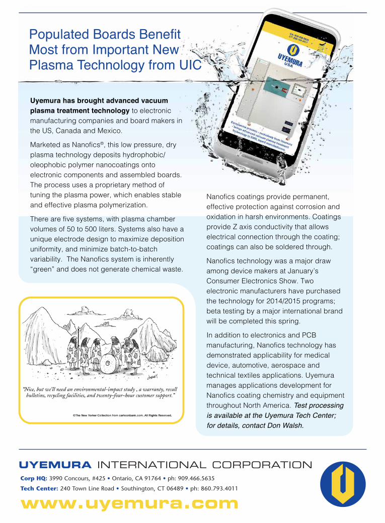
Uyemura has brought advanced vacuum plasma treatment technology to electronic manufacturing companies and board makers in the US, Canada and Mexico.
Marketed as Nanofics®, this low pressure, dry plasma technology deposits hydrophobic/ oleophobic polymer nanocoatings onto electronic components and assembled boards. The process uses a proprietary method of tuning the plasma power, which enables stable and effective plasma polymerization.
There are five systems, with plasma chamber volumes of 50 to 500 liters. Systems also have a unique electrode design to maximize deposition uniformity, and minimize batch-to-batch variability. The Nanofics system is inherently “green” and does not generate chemical waste.
Nanofics coatings provide permanent, effective protection against corrosion and oxidation in harsh environments. Coatings provide Z axis conductivity that allows electrical connection through the coating; coatings can also be soldered through.
Nanofics technology was a major draw among device makers at January’s Consumer Electronics Show. Two electronic manufacturers have purchased the technology for 2014/2015 programs; beta testing by a major international brand will be completed this spring.
In addition to electronics and PCB manufacturing, Nanofics technology has demonstrated applicability for medical device, automotive, aerospace and technical textiles applications. Uyemura manages applications development for Nanofics coating chemistry and equipment throughout North America. Test processing is available at the Uyemura Tech Center; for details, contact Don Walsh.
Populated Boards BenefitMost from Important NewPlasma Technology from UIC