Philips RF Manual - NXP Semiconductors | Automotive, … · 2016-02-22 · Circuit (MMIC). Due to...
66
Philips RF Manual product & design manual for RF small signal discretes 3 rd edition July 2003 APPENDIX http://www.philips.semiconductors.com/markets/mms/products/discretes/ documentation/rf_manual Document number: 4322 252 06385 Date of release: July 2003
Transcript of Philips RF Manual - NXP Semiconductors | Automotive, … · 2016-02-22 · Circuit (MMIC). Due to...

PhilipsRF Manualproduct & design manual for
RF small signal discretes
3rd editionJuly 2003
APPENDIXhttp://www.philips.semiconductors.com/markets/mms/products/discretes/
documentation/rf_manual
Document number: 4322 252 06385Date of release: July 2003

RF Manual APPENDIX App. Page: 2
3rd edition
Content appendix:
Appendix A: 2.4GHz Generic Front-End demoboard App. page: 3
Application notes:
Appendix B: BB202, low voltage FM stereo radio App. page: 27Appendix C: RF switch for e.g. Bluetooth application App. page: 33Appendix D: Application: the RF Switch BF1107/8 Mosfet App. page: 40Appendix E: Application of Dual-Gate Mosfets App. page: 51Appendix F: WCDMA applications for BGA6589 App. page: 62
RF Manual APPENDIX App. Page: 3
3rd edition
Appendix A 2.4GHz Gen. Front-End Demoboard
1.1. Introduction1.1.1. Description of a generic Front-End
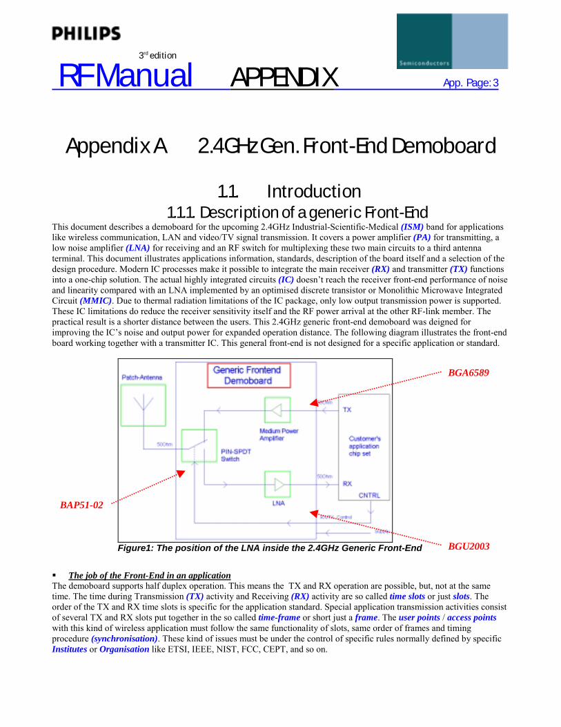
This document describes a demoboard for the upcoming 2.4GHz Industrial-Scientific-Medical (ISM) band for applicationslike wireless communication, LAN and video/TV signal transmission. It covers a power amplifier (PA) for transmitting, alow noise amplifier (LNA) for receiving and an RF switch for multiplexing these two main circuits to a third antennaterminal. This document illustrates applications information, standards, description of the board itself and a selection of thedesign procedure. Modern IC processes make it possible to integrate the main receiver (RX) and transmitter (TX) functionsinto a one-chip solution. The actual highly integrated circuits (IC) doesn’t reach the receiver front-end performance of noiseand linearity compared with an LNA implemented by an optimised discrete transistor or Monolithic Microwave IntegratedCircuit (MMIC). Due to thermal radiation limitations of the IC package, only low output transmission power is supported.These IC limitations do reduce the receiver sensitivity itself and the RF power arrival at the other RF-link member. Thepractical result is a shorter distance between the users. This 2.4GHz generic front-end demoboard was deigned forimproving the IC’s noise and output power for expanded operation distance. The following diagram illustrates the front-endboard working together with a transmitter IC. This general front-end is not designed for a specific application or standard.
The job of the Front-End in an applicationThe demoboard supports half duplex operation. This means the TX and RX operation are possible, but, not at the sametime. The time during Transmission (TX) activity and Receiving (RX) activity are so called time slots or just slots. Theorder of the TX and RX time slots is specific for the application standard. Special application transmission activities consistof several TX and RX slots put together in the so called time-frame or short just a frame. The user points / access pointswith this kind of wireless application must follow the same functionality of slots, same order of frames and timingprocedure (synchronisation). These kind of issues must be under the control of specific rules normally defined by specificInstitutes or Organisation like ETSI, IEEE, NIST, FCC, CEPT, and so on.
Figure1: The position of the LNA inside the 2.4GHz Generic Front-End
BAP51-02
BGU2003
BGA6589
RF Manual APPENDIX App. Page: 4
3rd edition
How does the Front-End work?Under the control (CNTRL-Pin) of customer’s chip set, the Front-End SPDT (single pole double through) Switch based onthe PIN Diode BAP51-02 closes the path between the antenna and the Medium Power Amplifier in the TX time slot. Theoutput power signals can be radiated from the antenna away into the Ether/Space. The Ether is the natural environmentmedium around being used by the wireless RF travelling waves from one access point to the other one. Because the TXsignals are amplified by the Medium Power Amplifier BGA6589, more powerful signals can be transmitted and reachfurther distances.The signal receiving occurs during the RX time slot. For this operation mode, the antenna is switched away from the PA(power amplifier) and connected to the LNA input under the control of the CNTRL-Pin. System analysis of the noiseperformance of a complete receiver show that a low noise amplifier (LNA) BGU2003 can improve the receiver sensitivityby reduction the effective RX system noise figure (NF). This is done by installing moderate gain with very low noise in thefront of the noisy IC receiver input by the use of the LNA. The effect is the receiver’s ability to properly receive signalsfrom access points at much further distances. This effect can be shown by the mathematical relationship shown below :
With the general Noise Figure (NF) definition:
=⋅=
Noise
Noise
PinPoutFNF log10)log(10 . All the time, the amount of the
noise ratio F will be larger than one (F>1 or NF>0dB) for operating at temperature larger than zero degree Kelvin.
The overall System Noise Ratio of the cascade LNA + RX chip results in: LNA
RXLNASYST Gain
FFF 1−+= The FSYST illustrates
that the overall system noise ratio (LNA+RX chip set) is at least the FLNA. There is the addition of a second amount of noisecaused by the ICs RX channel. But this amount is reduced by the LNA gain GainLNA. Use of moderate LNA does reduce thenoise ratio part of the receiver chip set. In this kind of relationship the LNA’s noise ratio FLNA is dominant.
Example-1: Issue: Customer’s receiver chip-set with a NF=9dB; LNA with Power Gain=13dB and NF=1.3dB Question: What’s the amount of the system receiver’s noise figure? Calculation:
2010 1013
==dB
LNAGain
943.710 109
==dB
RXF LNA-noise part
349.110 103.1
==dB
LNAF Reduced RX chip-set noise part
347.0349.120
1943.7349.11 +=−+=−+=LNA
RXLNASYST Gain
FFF
696.1=SYSTF
)696.1log(10)log(10 == SYSTSYST FNFdBNFSYST 3.2=
Answer: In this example the use of the LNA in front of the receiver chip-set does improve the overall receiver systemnoise figure to NF=2.3dB. The equations show that the first device in a cascade of objects has the most effecton the overall noise figure. In reality the first part of a receiver is the antenna. Its quality is very important.

RF Manual APPENDIX App. Page: 5
3rd edition
Example-2:Philips Medium Power MMICs portfolio offer the following listed insertion power gain |S21|2 performances:BGA6289 12dBBGA6589 15dB
Question:What is the expected approximated increase of distance using this Philips’ MMICs negating the attenuation of the Etherfrom an antenna with 3D homogenous round around field radiation in front of the chip-set?
Calculation:3D homogenous round around radiation power is general done by an ideal spherical dot. The theoretical reference isotropicantenna’s travelling damped wave power-density radiation is described by the general Physical law:
rESrE e
rAPP ⋅−⋅
⋅⋅⋅= χ
π 2)( 41
PE(r) = Receiver power in the distance “r” to the transmitter’s isotropic antennar = Distance receiver-transmitterPS = Transmitter powerχ = Atmospheric attenuation exponentAE = Receiver antenna surface
This kind of general Physic’s law is used for all kinds of spherical wave and energy radiation topics like in optics, acoustics,thermal, electromagnetic and so on. The job of the electromagnetic wave radiating antenna is the power matching of thecable impedance (50Ω, 75Ω,...) to the space’s impedance with the (ideal) electromagnetic far field impedance of 120πΩ.The received normalised power/unit area Pr at the receiver transmitted from a transmitter with the power Pt in the distance d
and neglecting of atmospheric attenuation (χ=0) is calculated by: 24 dPP TX
RX ⋅=
π
TX-RX-distance: r
t
PPd⋅
=π4
without PA: r
t
PPd⋅
=π4
11
Expanded distance by the PA for same received RX power: r
t
PPd⋅
=π4
22
2
1
2
1
2 21
4
4S
PP
PP
dd
r
t
r
t
=
⋅
⋅==
π
πη 221S=η
BGA6289 gain factor: 85.1510 1012
=dB
BGA6589 gain factor: 62.3110 1015
=dB
98.385.156289 ==BGAη 62.562.316589 ==BGAη
Answer:Use of BGA6289 can theoretical increase the transmitter operation area by the factor of 4. The BGA6589 can increase theoperation area by 5.6 assuming no compression of the amplifiers and an isotropic antenna radiator. In reality we have totake into account the amplifier input/output matching circuits adding or removing of gain to device’s insertion power gain,the frequency depending attenuation of the Ether and the gain of the receiver and transmitter antenna.
Improvment on the TX distance versus PA gain
1
10
100
0 6 12 18 24 30 36Gain/dB
=η=

RF Manual APPENDIX App. Page: 6
3rd edition
1.1.2. Applications for the demoboard
Some application ideas for the use of the Generic Front-End Demoboard
2.4GHz WLAN Wireless video, TV and remote control signal transmission PC to PC data connection PC headsets PC wireless mouse, key board, and printer Palm to PC, Keyboard, Printer connectivity Supervision TV camera signal transmission Wireless loudspeakers Robotics Short range underground walky-talky Short range snow and stone avalanche person detector Key less entry Identification Tire pressure systems Garage door opener Remote control for alarm-systems Intelligent kitchen (cooking place, Microwave cooker and washing machine operator reminder) Bluetooth DSSS 2.4GHz WLAN (IEEE802.11b) OFDM 2.4GHz WLAN (IEEE802.11g) Access Points PCMCIA PC Cards 2.4GHz Cordless telephones Wireless pencil as an input for Palms and PCs Wireless hand scanner for a Palm Identification for starting the car engine Wireless reading of gas counters Wireless control of soft-drink /cigarette/snag - SB machine Communication between bus/taxi and the stop lights Panel for ware house stock counting Printers Mobiles Wireless LCD Display Remote control Cordless Mouse Automotive, Consumer, Communication
Please note:The used MMICs and PIN diodes can be used in other frequency ranges e.g. 300MHz to 3GHz for applications likecommunication, networking and ISM too.
RF Manual APPENDIX App. Page: 7
3rd edition
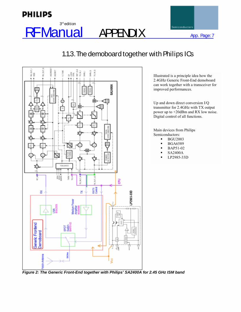
1.1.3. The demoboard together with Philips ICs
Figure 2: The Generic Front-End together with Philips’ SA2400A for 2.45 GHz ISM band
Illustrated is a principle idea how the2.4GHz Generic Front-End demoboardcan work together with a transceiver forimproved performances.
Up and down direct conversion I/Qtransmitter for 2.4GHz with TX outputpower up to +20dBm and RX low noise.Digital control of all functions.
Main devices from PhilipsSemiconductors:
BGU2003 BGA6589 BAP51-02 SA2400A LP2985-33D
RF Manual APPENDIX App. Page: 8
3rd edition
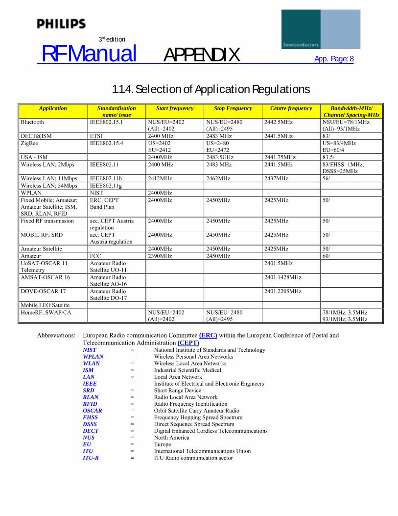
1.1.4. Selection of Application RegulationsApplication Standardisation
name/ issueStart frequency Stop Frequency Centre frequency Bandwidth-MHz/
Channel Spacing-MHzBluetooth IEEE802.15.1 NUS/EU=2402
(All)=2402NUS/EU=2480(All)=2495
2442.5MHz NSU/EU=78/1MHz(All)=93/1MHz
DECT@ISM ETSI 2400 MHz 2483 MHz 2441.5MHz 83/ZigBee IEEE802.15.4 US=2402
EU=2412US=2480EU=2472
US=83/4MHzEU=60/4
USA - ISM 2400MHz 2483.5GHz 2441.75MHz 83.5/Wireless LAN; 2Mbps IEEE802.11 2400 MHz 2483 MHz 2441.5MHz 83/FHSS=1MHz;
DSSS=25MHzWireless LAN; 11Mbps IEEE802.11b 2412MHz 2462MHz 2437MHz 56/Wireless LAN; 54Mbps IEEE802.11gWPLAN NIST 2400MHzFixed Mobile; Amateur;Amateur Satellite; ISM,SRD, RLAN, RFID
ERC, CEPTBand Plan
2400MHz 2450MHz 2425MHz 50/
Fixed RF transmission acc. CEPT Austriaregulation
2400MHz 2450MHz 2425MHz 50/
MOBIL RF; SRD acc. CEPTAustria regulation
2400MHz 2450MHz 2425MHz 50/
Amateur Satellite 2400MHz 2450MHz 2425MHz 50/Amateur FCC 2390MHz 2450MHz 60/UoSAT-OSCAR 11Telemetry
Amateur RadioSatellite UO-11
2401.5MHz
AMSAT-OSCAR 16 Amateur RadioSatellite AO-16
2401.1428MHz
DOVE-OSCAR 17 Amateur RadioSatellite DO-17
2401.2205MHz
Mobile LEO SateliteHomeRF; SWAP/CA NUS/EU=2402
(All)=2402NUS/EU=2480(All)=2495
78/1MHz, 3.5MHz93/1MHz, 3.5MHz
Abbreviations: European Radio communication Committee (ERC) within the European Conference of Postal andTelecommunication Administration (CEPT)NIST = National Institute of Standards and TechnologyWPLAN = Wireless Personal Area NetworksWLAN = Wireless Local Area NetworksISM = Industrial Scientific MedicalLAN = Local Area NetworkIEEE = Institute of Electrical and Electronic EngineersSRD = Short Range DeviceRLAN = Radio Local Area NetworkRFID = Radio Frequency IdentificationOSCAR = Orbit Satellite Carry Amateur RadioFHSS = Frequency Hopping Spread SpectrumDSSS = Direct Sequence Spread SpectrumDECT = Digital Enhanced Cordless TelecommunicationsNUS = North AmericaEU = EuropeITU = International Telecommunications UnionITU-R = ITU Radio communication sector

RF Manual APPENDIX App. Page: 9
3rd edition
1.2. Summary
1.2.1. Block Diagram
Figure 3: Block Diagram of the Demoboard

RF Manual APPENDIX App. Page: 10
3rd edition
1.2.2. Schematic
Figure 4: Schematic of the demoboard

RF Manual APPENDIX App. Page: 11
3rd edition
1.2.3. Part List
PartNumber
Value Size Function / Short explanation Manufacturer Order Code Ordersource
IC1 BGU2003 SOT363 LNA-MMIC Philips Semiconductors BGU2003 PHLIC2 BGA6589 SOT89 TX-PA-MMIC Philips Semiconductors BGA6589 PHLQ1 PBSS5140T SOT23 TX PA-standby control Philips Semiconductors PBSS5140T PHLQ2 BC847BW SOT323 LNA MMIC active Philips Semiconductors BC847BW PHLQ3 BC857BW SOT323 SPDT switching (NPN/PNP double transistor) Philips Semiconductors BC857BW PHLD1 BAP51-02 SOD523 SPDT-TX; series PIN Philips Semiconductors BAP51-02 PHLD2 BAP51-02 SOD523 SPDT-RX; shunt PIN Philips Semiconductors BAP51-02 PHLD3 LYR971 0805 LED, yellow, RX OSRAM 67S5126 BürklinD4 LYR971 0805 LED, yellow; TX OSRAM 67S5126 BürklinD5 LYR971 0805 LED, yellow; SPDT; voltage level shifter OSRAM 67S5126 BürklinD6 BZV55-B5V1 SOD80C Level shifting for being 3V/5V tolerant Philips Semiconductors BZV55-B5V1 PHLD7 BZV55-B10 SOD80C Board DC polarity & over voltage protection Philips Semiconductors BZV55-B10 PHLD8 BZV55-C3V6 SOD80C Board DC polarity & over voltage protection Philips Semiconductors BZV55-C3V6 PHLD9 BZV55-C3V6 SOD80C Board DC polarity & over voltage protection Philips Semiconductors BZV55-C3V6 PHLR1 150Ω 0402 SPDT bias Yageo RC0402 Vitrohm512 26E558 BürklinR2 1k8 0402 LNA MMIC current CTRL Yageo RC0402 Vitrohm512 26E584 BürklinR3 optional 0402 L2 resonance damping; optional optionalR4 47Ω 0402 LNA MMIC collector bias Yageo RC0402 Vitrohm512 26E546 BürklinR5 270Ω 0402 LED current adj. Yageo RC0402 Vitrohm512 26E564 BürklinR6 optional 0402R7 39k 0402 Q3 bias SPDT Yageo RC0402 Vitrohm512 26E616 BürklinR8 150Ω 0805 PA-MMIC collector current adjust and
temperature compensationYageo RC0805 Vitrohm503 11E156 Bürklin
R9 39k 0402 Helps switch of f of Q1 Yageo RC0402 Vitrohm512 26E616 BürklinR10 2.2kΩ 0402 Q1 bias PActrl Yageo RC0402 Vitrohm512 26E586 BürklinR11 1kΩ 0402 LED current adjust; TX-PA Yageo RC0402 Vitrohm512 26E578 BürklinR12 82k 0402 Q2 drive Yageo RC0402 Vitrohm512 26E624 BürklinR13 150Ω 0805 PA-MMIC collector current adjust Yageo RC0805 Vitrohm503 11E156 BürklinR14 150Ω 0805 PA-MMIC collector current adjust Yageo RC0805 Vitrohm503 11E156 BürklinR15 4k7 0402 Improvement of SPDT-Off Yageo RC0402 Vitrohm512 26E594 BürklinL1 22nH 0402 SPDT RF blocking for biasing Würth Elektronik, WE-MK 74478422 WEL2 4.7nH (shorted) 0402 LNAout matching Würth Elektronik, WE-MK 744784047 WEL3 18nH 0402 PAout Matching Würth Elektronik, WE-MK 74478418 WEL4 2.7nH 0402 LNA input match Würth Elektronik, WE-MK 744784022 WEL5 6.8nH 0402 Optional optimising of the PA input Würth Elektronik, WE-MK 744784068 WE

RF Manual APPENDIX App. Page: 12
3rd edition
PartNumber
Value Size Function / short explanation Manufacturer Order Code Ordersource
C1 1nF 0402 medium RF short for SPDT bias Murata, X7R GRP155R71H102KA01B MurataC2 6.8pF 0402 medium RF short for SPDT bias Murata, C0G GRP1555C1H6R8DZ01B MurataC3 6.8pF 0402 Antenna DC decoupling Murata, C0G GRP1555C1H6R8DZ01B MurataC4 2.2pF 0402 RF short SPDT shunt PIN Murata, C0G GRP1555C1H2R2CZ01B MurataC5 4.7pF 0402 DC decoupling LNA input + match Murata, C0G GRP1555C1H4R7CZ01B MurataC6 4.7pF 0402 RF short output match Murata, C0G GRP1555C1H4R7CZ01B MurataC7 1pF 0402 LNA output matching Murata, C0G GRP1555C1H1RCZ01B MurataC8 10uF/10V A Removes the line ripple together with
R8-R14Epcos, HighCapB45196H2106+10 *
25D1820 Bürklin
C9 100nF 0603 Ripple rejection PA no name internal stock BürklinC10 47pF 0402 DC decoupling PA input Murata, C0G GRP1555C1H470JZ01B MurataC11 22pF 0402 RF short-bias PA AVX, 1B/C0G/NP0 04025A220JAT2A AVXC12 1nF 0402 RF short-bias Murata, X7R GRP155R71H102KA01B MurataC13 2.2uF/16V
optionalA RF short; not used because switch on of PA
will be delayed but don’t removes lineripple; maybe optional for ext. Vcc
Epcos, Tantal SMD Standard;B45196E2225K109
25D1020internal stock
Bürklin
C14 2.2pF 0402 TX-PAout DC decoupling + matching Murata, C0G GRP1555C1H2R2CZ01B MurataC15 10u/10V A dc rail LNVcc Epcos, HighCap
B45196H2106+10 *25D1820 Bürklin
C16 1.2nF 0603 dc noise LNctrl no name internal stock BürklinC17 2.2uF/10V A dc rail Epcos, Tantal SMD Standard;
B45196E2225K10925D1020 Bürklin
C18 1.2nF 0603 dc noise SPDT no name internal stock BürklinC19 1.2nF 0603 dc noise PActrl no name internal stock BürklinC20 1.2nF 0603 dc noise LNVcc no name internal stock BürklinC21 4.7pF 0402 RF short for optional LNA input match Murata, C0G GRP1555C1H4R7CZ01B MurataPCB FR4 compatible 45mm X
40mmEpoxy 560µm; Cu=17.5µm;Ni=5µm; Au=0.3µmtwo layer double side
www.isola.deHäfele Leiterplattentechnik
DURAVER®-E-Cu,Qualität 104 MLB-DE 104 ML/2
Häfele
X1 SMA, female pin Microstrip Antenna connector Huber+Suhner, panellauncher, female, tab contact
23 SMA-50-0-2/111 NE Suhner
X2 SMA, female pin Microstrip RX-Out connector Huber+Suhner, panellauncher, female, tab contact
23 SMA-50-0-2/111 NE Suhner
X3 SMA, female pin Microstrip TX-IN connector Huber+Suhner, panellauncher, female, tab contact
23 SMA-50-0-2/111 NE Suhner

RF Manual APPENDIX App. Page: 13
3rd edition
1.2.4. The PCB
RF Manual APPENDIX App. Page: 14
3rd edition
1.2.5. Functional description
1.2.5.1. Principle of operation
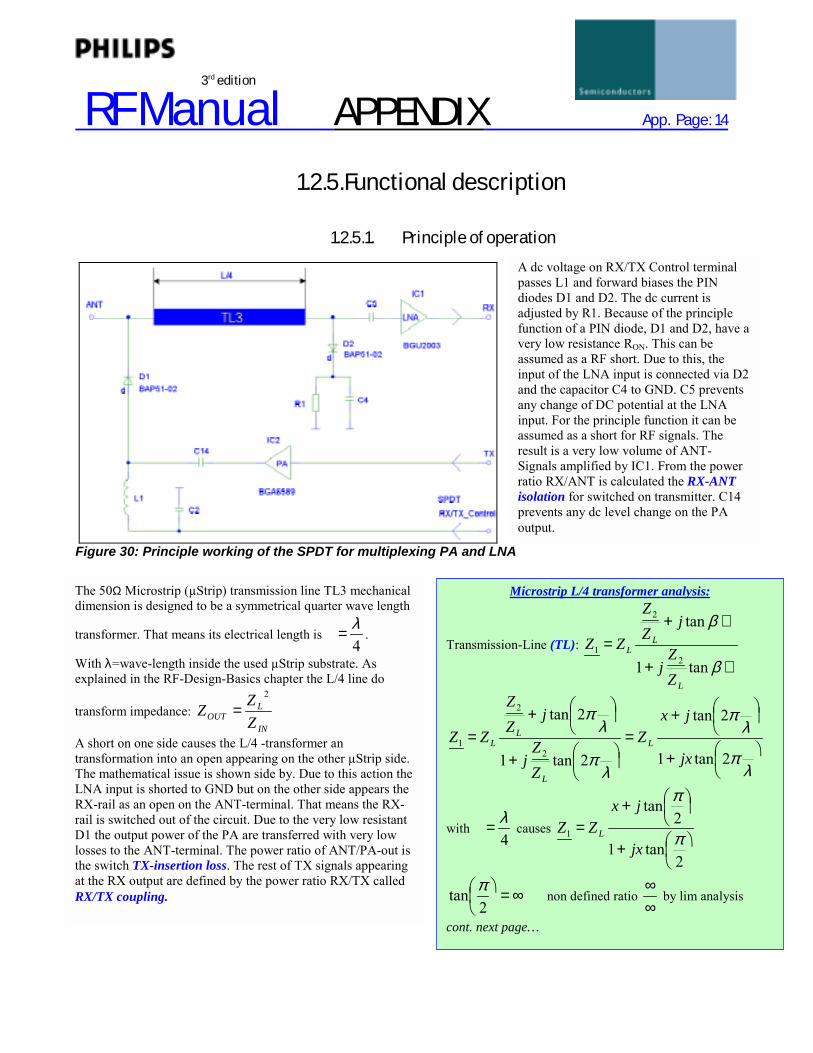
Figure 30: Principle working of the SPDT for multiplexing PA and LNA
A dc voltage on RX/TX Control terminalpasses L1 and forward biases the PINdiodes D1 and D2. The dc current isadjusted by R1. Because of the principlefunction of a PIN diode, D1 and D2, have avery low resistance RON. This can beassumed as a RF short. Due to this, theinput of the LNA input is connected via D2and the capacitor C4 to GND. C5 preventsany change of DC potential at the LNAinput. For the principle function it can beassumed as a short for RF signals. Theresult is a very low volume of ANT-Signals amplified by IC1. From the powerratio RX/ANT is calculated the RX-ANTisolation for switched on transmitter. C14prevents any dc level change on the PAoutput.
The 50Ω Microstrip (µStrip) transmission line TL3 mechanicaldimension is designed to be a symmetrical quarter wave length
transformer. That means its electrical length is 4λ= .
With λ=wave-length inside the used µStrip substrate. Asexplained in the RF-Design-Basics chapter the L/4 line do
transform impedance: IN
LOUT Z
ZZ2
=
A short on one side causes the L/4 -transformer antransformation into an open appearing on the other µStrip side.The mathematical issue is shown side by. Due to this action theLNA input is shorted to GND but on the other side appears theRX-rail as an open on the ANT-terminal. That means the RX-rail is switched out of the circuit. Due to the very low resistantD1 the output power of the PA are transferred with very lowlosses to the ANT-terminal. The power ratio of ANT/PA-out isthe switch TX-insertion loss. The rest of TX signals appearingat the RX output are defined by the power ratio RX/TX calledRX/TX coupling.
Microstrip L/4 transformer analysis:
Transmission-Line (TL):
⋅+
⋅+=
β
β
tan1
tan
2
2
1
L
LL
ZZ
j
jZZ
ZZ
+
+=
+
+=
λπ
λπ
λπ
λπ
2tan1
2tan
2tan1
2tan
2
2
1
jx
jxZ
ZZ
j
jZZ
ZZ L
L
LL
with 4λ= causes
+
+=
2tan1
2tan
1 π
π
jx
jxZZ L
∞=
2tan π
non defined ratio ∞∞
by lim analysis
cont. next page…
RF Manual APPENDIX App. Page: 15
3rd edition
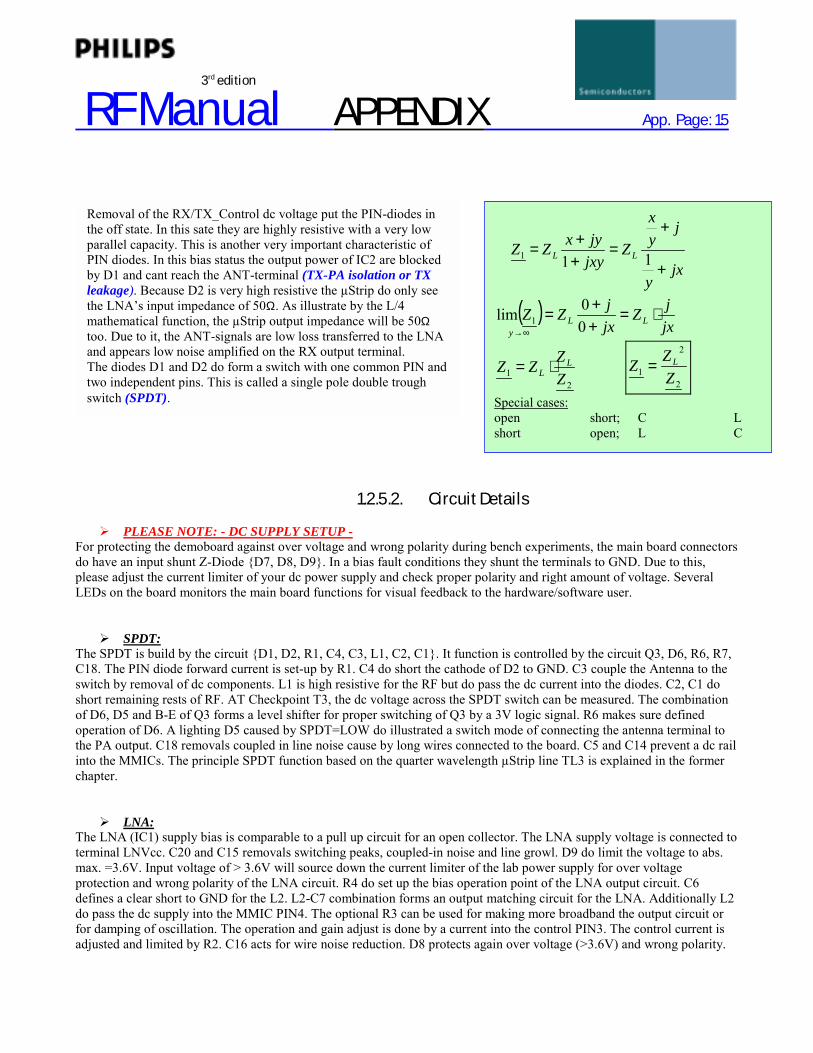
1.2.5.2. Circuit Details PLEASE NOTE: - DC SUPPLY SETUP -
For protecting the demoboard against over voltage and wrong polarity during bench experiments, the main board connectorsdo have an input shunt Z-Diode D7, D8, D9. In a bias fault conditions they shunt the terminals to GND. Due to this,please adjust the current limiter of your dc power supply and check proper polarity and right amount of voltage. SeveralLEDs on the board monitors the main board functions for visual feedback to the hardware/software user.
SPDT:The SPDT is build by the circuit D1, D2, R1, C4, C3, L1, C2, C1. It function is controlled by the circuit Q3, D6, R6, R7,C18. The PIN diode forward current is set-up by R1. C4 do short the cathode of D2 to GND. C3 couple the Antenna to theswitch by removal of dc components. L1 is high resistive for the RF but do pass the dc current into the diodes. C2, C1 doshort remaining rests of RF. AT Checkpoint T3, the dc voltage across the SPDT switch can be measured. The combinationof D6, D5 and B-E of Q3 forms a level shifter for proper switching of Q3 by a 3V logic signal. R6 makes sure definedoperation of D6. A lighting D5 caused by SPDT=LOW do illustrated a switch mode of connecting the antenna terminal tothe PA output. C18 removals coupled in line noise cause by long wires connected to the board. C5 and C14 prevent a dc railinto the MMICs. The principle SPDT function based on the quarter wavelength µStrip line TL3 is explained in the formerchapter.
LNA:The LNA (IC1) supply bias is comparable to a pull up circuit for an open collector. The LNA supply voltage is connected toterminal LNVcc. C20 and C15 removals switching peaks, coupled-in noise and line growl. D9 do limit the voltage to abs.max. =3.6V. Input voltage of > 3.6V will source down the current limiter of the lab power supply for over voltageprotection and wrong polarity of the LNA circuit. R4 do set up the bias operation point of the LNA output circuit. C6defines a clear short to GND for the L2. L2-C7 combination forms an output matching circuit for the LNA. Additionally L2do pass the dc supply into the MMIC PIN4. The optional R3 can be used for making more broadband the output circuit orfor damping of oscillation. The operation and gain adjust is done by a current into the control PIN3. The control current isadjusted and limited by R2. C16 acts for wire noise reduction. D8 protects again over voltage (>3.6V) and wrong polarity.
Removal of the RX/TX_Control dc voltage put the PIN-diodes inthe off state. In this sate they are highly resistive with a very lowparallel capacity. This is another very important characteristic ofPIN diodes. In this bias status the output power of IC2 are blockedby D1 and cant reach the ANT-terminal (TX-PA isolation or TXleakage). Because D2 is very high resistive the µStrip do only seethe LNA’s input impedance of 50Ω. As illustrate by the L/4mathematical function, the µStrip output impedance will be 50Ωtoo. Due to it, the ANT-signals are low loss transferred to the LNAand appears low noise amplified on the RX output terminal.The diodes D1 and D2 do form a switch with one common PIN andtwo independent pins. This is called a single pole double troughswitch (SPDT).
jxy
jyx
ZjxyjyxZZ LL
+
+=
++= 111
( )jxjZ
jxjZZ LL
y
⋅=++=
∞→ 00lim 1
21 Z
ZZZ LL ⋅=
2
2
1 ZZZ L=
Special cases:open short; C Lshort open; L C

RF Manual APPENDIX App. Page: 16
3rd edition
With LNctrl=HIGH, the LNA is switched on with max. Gain. This is illustrated by lighting D3. LNctrl voltages between 0Vand 3.0V can be used for standby, max. Gain and variable gain like AGC. The voltage potential difference between LNctrland test point T5 (across R2) can be used for calculating the actual control current into PIN3. Depending on the amount ofR12 the LED. D3 do illustrate the actual LNA-Gain. Because the LNA input impedance and noise optimum impedance areclosed to 50Ω there is no further need of input matching circuit. C5 do removal dc components. If there is the need forfurther experimental input matching experiments, the combination of C5 and the optional L4-C21 can be used by thecustomer.
PA:The power amplifier MMIC (IC2) does it self need a supply of ca. 4.7V/83mA sinking into the output PIN3. Fortemperature stabilisation of the output voltage-current temperature relationship, there is the need of series resistors R8,R13, R14. L3 do inject the dc supply current into the MMIC. Additionally L3 blocks the RF. RF leakage behind it is shuntto GND by C11. C12 do back up for medium frequencies and ripples caused by e.g. large output envelope change. At testpoint T2 can be monitored the PA output dc voltage. By the use of Q1, R10, C19 the PA can be switched off. For an openterminal PActrl, R9 makes sure of full conducting Q1. D4 do light for switched on power amplifier. The optional L5 can beused for input matching optimisation experiments. D7 do protect the PA against over voltage on wrong polarity.

RF Manual APPENDIX App. Page: 17
3rd edition
1.3. Data Sheet “2.4GHz Generic Front-End”Philips Semiconductors European Support Group Objective specification
2003 May 15
2.4GHz Generic Front-End Demoboard BGA6589, BGU2003,BAP51-02
FEATURES
2.4GHz ISM band operation 50Ω female SMA connectors LNA, PA and SPDT on board Supply control function LED’s indicates the operation mode
APPLICATIONS
Bluetooth W-LAN ISM Home video and TV link Remote control
DESCRIPTION
The demoboard is intended to be used as a generic Front-EndModule in front of a high integrated half duplex IC chip set.It uses an LNA-MMIC (BGU2003) for improving the receiverSensitivity and a PA-MMIC (BGA6589) for increasing thetransmitter distance. A controlled SPDT based on PIN-Diodes(BAP51-02) switch the LNA or the PA to the common antennaterminal e.g. a 50Ω ceramic patch antenna can be connected.
Note:1. USL=Upper Spec Limit; LSL=Lower Spec Limit2. USL and LSL are calculated according Philips’ 6-Sigma Statistic Process Control (SPC) definition for Cp=2.03. MIN and MAX data are determined by the max. spread measured on 10 investigated demoboards
PINNING
PIN / PORT DESKRIPTIONANT Bi-directional Antenna
I/OGND GroundLNctrl LNA controlLNVcc LNA dc supplyRX LNA 50Ω outSPDT SPDT control RX/TXPAVcc PA dc supplyPActrl PA controlTX PA control
Fig.1 Demoboard Top View

RF Manual APPENDIX App. Page: 18
3rd edition
QUICK REFERENCE DATA
SYMBOL PARAMETER CONDITIONS MIN. TYP. MAX. UNITBW bandwidth 2401 2498.5 MHzPAVcc DC supply voltage PA 9 VLNVcc DC supply voltage LNA 3 VI(PAVcc) supply current PA mAI(LNVcc) LNA mAI(stby) standby supply current I (PAVcc)+ I(LNVcc) µA
LNA receive (RX) dBS21 forward power gainPA transmit (TX) dB
NF noise figure 2450MHz, LNA tbf dBLNA output; 2450MHz +9.1 dBmPL 1dB load power at 1dB gain
compression PA output; 2450MHz +16.9 dBm
LIMITING VALUES
SYMBOL PARAMETER CONDITIONS MIN. TYP. MAX. UNITPAVcc DC supply voltage PA; note 1 0 9 10 VLNVcc DC supply voltage LNA; note 1 0 3 3.6 VSPDT SPDT switch control 0 0/3/5 PAVcc VLNctrl LNA power control note 1 0 0/3 3.6 VPActrl PA power control 0 0/9 PAVcc V
Note:1. The board is protected by a Z-Diode to GND. Negative voltages or voltage at the limit do cause this diode
to shunt a large current to GND. This is for protecting the board against wrong polarity and over voltage during bench experiments.
ACTIVE DEVICES THERMAL CHARACTERISTICS
SYMBOL PARAMETER CONDITIONS VALUE UNITBGA6589, TS≤70 °C; note 1 100BGU2003 85
R th j-s thermal resistance fromjunction to solder point
BAP51-02 350BC847BW; note 2 625BC857BW; note 3 625
in free air; note 4 417
R th j-a thermal resistance fromjunction to ambient
PBSS5140Tin free air; note 5 278
K/W
Note:1. TS is the temperature at the soldering point of pin 4.2. Transistor mounted on an FR4 printed-circuit board.3. Refer to SOT323 standard mounting conditions.4. Device mounted on a printed-circuit board, single sided copper, tinplated and standard footprint.5. Device mounted on a printed-circuit board, single sided copper, tinplated and mounting pad for
collector 1cm2.
RF Manual APPENDIX App. Page: 19
3rd edition
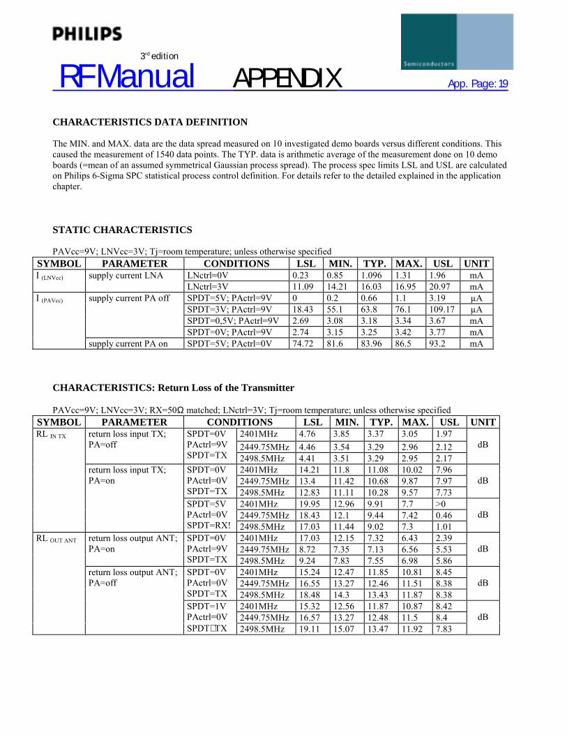
CHARACTERISTICS DATA DEFINITION
The MIN. and MAX. data are the data spread measured on 10 investigated demo boards versus different conditions. Thiscaused the measurement of 1540 data points. The TYP. data is arithmetic average of the measurement done on 10 demoboards (=mean of an assumed symmetrical Gaussian process spread). The process spec limits LSL and USL are calculatedon Philips 6-Sigma SPC statistical process control definition. For details refer to the detailed explained in the applicationchapter.
STATIC CHARACTERISTICS
PAVcc=9V; LNVcc=3V; Tj=room temperature; unless otherwise specifiedSYMBOL PARAMETER CONDITIONS LSL MIN. TYP. MAX. USL UNIT
LNctrl=0V 0.23 0.85 1.096 1.31 1.96 mAI (LNVcc) supply current LNALNctrl=3V 11.09 14.21 16.03 16.95 20.97 mASPDT=5V; PActrl=9V 0 0.2 0.66 1.1 3.19 µASPDT=3V; PActrl=9V 18.43 55.1 63.8 76.1 109.17 µASPDT=0,5V; PActrl=9V 2.69 3.08 3.18 3.34 3.67 mA
supply current PA off
SPDT=0V; PActrl=9V 2.74 3.15 3.25 3.42 3.77 mA
I (PAVcc)
supply current PA on SPDT=5V; PActrl=0V 74.72 81.6 83.96 86.5 93.2 mA
CHARACTERISTICS: Return Loss of the Transmitter
PAVcc=9V; LNVcc=3V; RX=50Ω matched; LNctrl=3V; Tj=room temperature; unless otherwise specifiedSYMBOL PARAMETER CONDITIONS LSL MIN. TYP. MAX. USL UNIT
2401MHz 4.76 3.85 3.37 3.05 1.972449.75MHz 4.46 3.54 3.29 2.96 2.12
return loss input TX;PA=off
SPDT=0VPActrl=9VSPDT=TX 2498.5MHz 4.41 3.51 3.29 2.95 2.17
dB
2401MHz 14.21 11.8 11.08 10.02 7.962449.75MHz 13.4 11.42 10.68 9.87 7.97
SPDT=0VPActrl=0VSPDT=TX 2498.5MHz 12.83 11.11 10.28 9.57 7.73
dB
2401MHz 19.95 12.96 9.91 7.7 >02449.75MHz 18.43 12.1 9.44 7.42 0.46
RL IN TX
return loss input TX;PA=on
SPDT=5VPActrl=0VSPDT=RX! 2498.5MHz 17.03 11.44 9.02 7.3 1.01
dB
2401MHz 17.03 12.15 7.32 6.43 2.392449.75MHz 8.72 7.35 7.13 6.56 5.53
return loss output ANT;PA=on
SPDT=0VPActrl=9VSPDT=TX 2498.5MHz 9.24 7.83 7.55 6.98 5.86
dB
2401MHz 15.24 12.47 11.85 10.81 8.452449.75MHz 16.55 13.27 12.46 11.51 8.38
SPDT=0VPActrl=0VSPDT=TX 2498.5MHz 18.48 14.3 13.43 11.87 8.38
dB
2401MHz 15.32 12.56 11.87 10.87 8.422449.75MHz 16.57 13.27 12.48 11.5 8.4
RL OUT ANT
return loss output ANT;PA=off
SPDT=1VPActrl=0VSPDT∼ TX 2498.5MHz 19.11 15.07 13.47 11.92 7.83
dB

RF Manual APPENDIX App. Page: 20
3rd edition
CHARACTERISTICS: Return Loss of the Receiver
PAVcc=9V; LNVcc=3V; RX=50Ω matched; LNctrl=3V; Tj=room temperature; unless otherwise specifiedSYMBOL PARAMETER CONDITIONS LSL MIN. TYP. MAX. USL UNIT
2401MHz 23.55 18.14 16.43 14.2 9.312449.75MHz 25.51 19.01 15.65 12.74 5.79
return loss input ANT;PA=off
SPDT=3VLNctrl=3VPActrl=9V 2498.5MHz 20.85 15.75 14.31 12 7.8
dB
2401MHz 15.29 12.31 11.21 10.15 7.142449.75MHz 16.61 13.09 11.87 10.66 7.13
SPDT=0VLNctrl=0VPActrl=0V 2498.5MHz 17.69 13.83 12.59 11.32 7.5
dB
2401MHz 23.93 18.35 16.64 14.28 9.342449.75MHz 22.92 16.99 15.55 12.92 8.18
RL IN ANT
return loss input ANT;PA=on
SPDT=3VLNctrl=3VPActrl=0V 2498.5MHz 21.38 15.95 14.53 12.1 7.67
dB
2401MHz 23.03 18 14.84 13.49 6.642449.75MHz 28.01 19.61 17.77 13.74 7.53
return loss output RX;PA=off
SPDT=3VLNctrl=3VPActrl=9V 2498.5MHz 32.59 20.86 17.69 11.41 2.79
dB
2401MHz 14.8 9.73 4.72 3.8 5.362449.75MHz 11.13 7.74 4.45 3.79 2.23
SPDT=0VLNctrl=0VPActrl=0V 2498.5MHz 8.87 6.41 4.06 3.52 >0
dB
2401MHz 22.84 17.9 14.93 13.64 7.012449.75MHz 28.4 19.78 17.95 13.8 7.5
RL OUT RX
return loss output RX;PA=on
SPDT=3VLNctrl=3VPActrl=0V 2498.5MHz 32.88 21.02 17.83 11.5 2.78
dB

RF Manual APPENDIX App. Page: 21
3rd edition
CHARACTERISTICS: RX and TX gain
PAVcc=9V; LNVcc=3V; Tj=room temperature; unless otherwise specifiedS21(TX): NWA Port1-IN TX; NWA Port2-ANT;RX=50Ω matchedS21 (TX/RX): NWA Port1-IN TX; Port2-Out RX; ANT=50ΩS12 (TX) : NWA Port1-IN TX; NWA Port2-ANT;RX=50Ω matched
SYMBOL PARAMETER CONDITIONS LSL MIN. TYP. MAX. USL UNIT2401MHz 13.95 14.75 14.98 15.33 16.022449.75MHz 13.89 14.63 14.87 15.2 15.85
SPDT=0VLNctrl=0VPActrl=0V 2498.5MHz 13.72 14.46 14.71 15.04 15.71
dB
2401MHz 13.96 14.76 15 15.34 16.032449.75MHz 13.88 14.65 14.89 15.23 15.9
S21 (TX) forward gain PAPA=on
SPDT=0VLNctrl=0VPActrl=3V 2498.5MHz 13.76 14.5 14.75 15.07 15.73
dB
2401MHz 25.44 24.66 24.27 24 23.092449.75MHz 25.22 24.5 24.09 23.8 22.96
S12 (TX) reverse gain PAPA=on
SPDT=0VLNctrl=0VPActrl=0V 2498.5MHz 25.08 24.29 23.93 23.6 22.78
dB
2401MHz 11.21 12.2 13.17 13.4 15.122449.75MHz 10.69 11.87 13.03 13.24 15.37
forward gain LNAPA=off
SPDT=3VLNctrl=9VPActrl=3V 2498.5MHz 10.08 11.43 12.77 12.96 15.46
dB
2401MHz 11.1 12.13 13.13 13.35 15.152449.75MHz 10.66 11.83 12.98 13.19 15.3
S21 (RX)
forward gain LNAPA=on
SPDT=3VLNctrl=0VPActrl=3V 2498.5MHz 10.06 11.39 12.72 12.92 15.37
dB
2401MHz 18.79 18.1 17.91 17.58 17.042449.75MHz 18.29 17.8 17.62 17.45 16.96
S12 (RX) reverse gain PAPA=on
SPDT=3VLNctrl=9VPActrl=3V 2498.5MHz 18.05 17.67 17.48 17.36 16.92
dB
2401MHz 6.45 8.37 9.36 10.21 12.282449.75MHz 6.22 8.16 9.36 10.2 12.5
S21 (TX/RX) coupling TX RXPA=LNA=on
SPDT=3VLNctrl=0VPActrl=3V 2498.5MHz 5.86 7.88 9.24 10.09 12.61
dB
CHARACTERISTICS: LNA out of band gain
For characterisation the sensitivity against received signals out side the 2.4GHz ISM band.
PAVcc=9V; LNVcc=3V; PActrl=9V; TX=50Ω matched; Tj=room temperature; unless otherwise specifiedSYMBOL PARAMETER CONDITIONS LSL MIN. TYP. MAX. USL UNIT
148.71MHz -14.58 -13.56 -13.21 -12.76 -11.83314.5MHz -9.57 -7.69 -7.28 -6.28 -5431.5MHZ -8.31 -6.53 -6.04 -5.08 -3.77899.5MHz -14.96 -13.07 -12.45 -11.87 -9.931903.75MHz -0.32 2.6 3.7 4.75 7.722449.75MHz 10.66 11.86 13.05 13.24 15.443600.25MHz 4.19 5.69 6.7 7.24 9.21
S21 (RX) forward gain LNA
4000MHz 3.81 4.91 5.6 6.03 7.38
dB

RF Manual APPENDIX App. Page: 22
3rd edition
LNA Output Power versus Input drive level at 2450MHz
-5
0
5
10
15
-15 -10 -5 0 5
Lin/[dBm]
Lout
/[dB
m]
MENMINMAXUSLLSL
LNA Output 1dB compression point analysis at 2450MHz
-5
0
5
10
15
-30 -25 -20 -15 -10 -5 0
Lin/[dBm]
Lout
/[dB
m];
Gai
n Er
ror/[
10*d
B]
MEN
10*GainError(MEN)
The 1dB compression point is found at a gain error of 1dB
LNA 1dB compression pointof the LNA at 2450MHz:PL1dB(IN)≈-2,2dBmPL1dB(OUT)≈+9,1dBmThis is an arithmetic averagevalue (TYP.)
LNA-PL1dB set-up:
LNVcc=3VPAVcc=9VSPDT=LNctrl=3V;PActrl=9VANT=hp8594E with 40dBattenuator fixed settingTX=SME03RX=50Ω match

RF Manual APPENDIX App. Page: 23
3rd edition
PA Output Power versus Input drive level at 2450MHz
0
5
10
15
20
-10 -5 0 5 10
Lin/[dBm]
Lout
/[dB
m]
MENMINMAXUSLLSL
PA Output 1dB compression point analysis at 2450MHz
-5
0
5
10
15
20
-10 -5 0 5 10
Lin/[dBm]
Lout
/[dB
m];
10*G
ainE
rror
(MEN
)/[dB
] MEN
10*GainError(MEN)
The 1dB compression point is found at a gain error of 1dB
LNA-PL1dB Setup:
LNVcc=3VPAVcc=9VSPDT=LNctrl=3V;PActrl=9VANT=hp8594E with 40dBattenuator fixed settingTX=SME03RX=50Ω match
PA 1dB compression point ofthe LNA at 2450MHz:PL1dB(IN)≈+3,8dBmPL1dB(OUT)≈+16,9dBmThis is an arithmetic averagevalue (TYP.)

RF Manual APPENDIX App. Page: 24
3rd edition
Port2=RX;Port1=ANT; TX=Match; PActrl=9V; SPDT=VAR ; LNctrl=3V
S21(LNA) control performance by the SPDT at 2449,75MHz
-15
-10
-5
0
5
10
15
20
0 1 2 3 4 5
V(SPDT)/V
S21/
[dB
]
MEN MINMAX USLLSL
Port2=ANT;Port1=TX; RX=Match; PActrl=0V; SPDT=VAR ; LNctrl=0V
S21(PA) control performance by the SPDT at 2449,75MHz
-10
-5
0
5
10
15
20
0 1 2 3 4 5
V(SPDT)/V
S21/
[dB
]
MEN MINMAX USLLSL

RF Manual APPENDIX App. Page: 25
3rd edition
Port2=RX;Port1=TX; ANT=Match; PActrl=0V; SPDT=VAR ; LNctrl=3V
S21(TX==>RX coupling) control performance by the SPDT at 2449,75MHz LNA=ON
0
5
10
15
20
0 1 2 3 4 5
V(SPDT)/V
S21/
[dB
]
MEN MINMAX USLLSL
Port2=RX;Port1=TX; ANT=Match; PActrl=0V; SPDT=VAR ; LNctrl=0V
S21(TX==>RX coupling) control performance by the SPDT at 2449,75MHz LNA=OFF
-35
-30
-25
-20
-15
-10
0 1 2 3 4 5
V(SPDT)/V
S21/
[dB
]
MEN MINMAX USLLSL
RF Manual APPENDIX App. Page: 26
3rd edition
1.4. Reference
Author:Andreas FixRF Discretes Small Signal Application Engineer
1) Philips Semiconductors, Data Sheet BGU2003, SiGe MMIC amplifier2) Philips Semiconductors, Data Sheet BGA6589, MMIC wideband medium power amplifier3) Philips Semiconductors, Data Sheet, BAP51-02, General Purpose PIN-Diode4) Philips Semiconductors, Application Note AN10173-01, 2.45 GHz T/R, RF switch for e.g.
bluetooth application using PIN diodes5) Deutsche Bundespost Telekom, Fachhochschule Dieburg, Physik, Prof. Dr. Lehnert, 19916) Telekom, Fachhochschule Dieburg, Hochfrequenztechnik, Prof. Dr.-Ing. K. Schmitt, 19937) TFH Berlin, Grundlagen der Elektrotechnik I, Prof. Dr. Suchaneck8) S. Gerhart, Technische Physik, Formeln und Tabellen, Paucke-Verlag, 19839) Hoff Seifert, Physik für Fachoberschulen, Schroeder, 1976. S.23410) www.isola.de; Datasheet B-DE104ML, DURAVER®-E-Cu, Qualität 104 ML11) Hubner+Suhner Data Sheet of 23SMA-50-0-2/111NE12) Failure Analysis labor at Rood Technology

RF Manual APPENDIX App. Page: 27
3rd edition
Appendix B: Application note BB202, low voltage FM stereo radio (TEA5767/68)
Author(s): M Ait Moulay , Philips Semiconductors Strategic Partnership CatenaThe Netherlands, Date: 18-06-2002
This is a shortened application note to emphasise the BB202 varicap as an important FM oscillator next to theTEA5767/68 single chip stereo FM receiver (complete application note: AN10133).
SummaryThe TEA5767/68 is a single-chip stereo FM receiver. This new generation, low-voltage FM radio hasa fully integrated IF with selectivity and demodulation. The IC does not require any alignment, whicheliminates bulky and expensive external components.The digital tuning approach is based on conventional PLL concepts. With software, the radio can betuned into the European, Japanese, or US FM bands.The power consumption for the tuner is low. Supply current is about 13 mA and supply voltage can bevaried between 2.5 and 5V.The radio finds applications in many areas, especially in portable applications such as mobile phonesand portable CD and MP3 players.This application note describes this FM radio in a small size and low voltage application. Todemonstrate the operation of the tuners a demonstration board is developed, which can be extendedwith a software controllable amplifier and a RDS chip. The complete application can be controlledfrom a PC by means of demonstration software.
IntroductionConsumer demand for more integrated and low power IC’s has increased tremendously in the last decade. The IC’s must besmaller, cheaper and consume less power. This is especially true for portable equipment like mobile phone, CD, MP3 andcassette players, where battery life and a large feature set is very important. To integrate an FM radio in this kind ofequipment it is important that the radio function be small and the overall power consumption of the radio function is low.The TEA5767/68 is a single chip, digitally tuned FM stereo radio. The device is small, has a very low current consumptionand is completely adjustment free. This simplifies the PCB design and saves design-in time. The tuner contains all theblocks necessary to build a complete digitally tuned radio function.
The FM tuners consist of three IC’s in 32 pins or 40 pins package. These IC’s can be controlled via either a 3-Wire or anI2C (or both) bus interface.A small PCB demonstration board has been designed on which any of the three IC’s can be mounted. These demo boardscan be placed on a motherboard, which can be extended with an audio amplifier and a Radio Data System (RDS/RBDS) IC.

RF Manual APPENDIX App. Page: 28
3rd edition
The three tuners are:• TEA5767HN FM stereo radio, 40 leads with I2C and 3-Wire bus interface, Body 6*6*0.85 mm, SOT1618• TEA5767HL FM stereo radio, 32 leads with 3-Wire bus interface, Body: 7*7*1.4 mm, SOT358.• TEA5768HL FM stereo radio, 32 leads with I2C bus interface, Body: 7*7*1.4 mm, SOT358.
In this application note only one IC, the TEA5767HN, and one demonstration board will be described.However, this description can be applied to the other boards.
1. The TEA5767A block diagram of the TEA5767HN is given in Figure 1. The block diagram consists of a number of blocks that will bedescribed according to the signal path from the antenna to the audio output.
The RF antenna signal is injected into a balanced low noise amplifier (LNA) via a RF matching circuit. In order not tooverload the LNA and the mixer the LNA output signal is fed to an automatic gain control circuit (AGC). In a quadraturemixer the RF signal is converted down to an IF signal of 225KHz by multiplying it with a local oscillator signal (LO). Thechosen mixer architecture provides inherent image rejection.The VCO generates a signal with double the frequency necessary for the I/Q mixer structure. In the N1 divider block, therequired LO signal is created. The frequency of the VCO is controlled with a PLL synthesiser system.The I/Q signals out the mixer are fed to an integrated IF filter (RESAMP block). The IF frequency of this filter is controlledby the IF Centre Frequency adjust block.The IF signal is then passed to the limiter block, which removes the amplitude variation from the signal. The limiter isconnected to the level ADC and the IF counter blocks. These two blocks provide the proper information about theamplitude and frequency of the RF input signal, which will be used by the PLL as stop criterion.The IC has a quadrature demodulator with an integrated resonator. The demodulator is fully integrated which makes IFalignments or an external resonator unnecessary.
GAINSTABI
POWERSUPPLY
LIMITERRESAMPDEMOD
x SOFTMUTE
IF COUNTLEVELADC
IF CenterFreq. Adjust
I/Q-MIXER1st FM
x:2N1
AGC
MP
X DEC
OD
ER
XTALOSC
SWPORTMUXTUNING SYSTEM
VCO I2C/3WIRE BUS
VCC
TEA5767HN
n.c
18KΩ
4.7Ω
22n 22u
100p
FM ANT
27p
47p120n
n.c.10n
39n10K
100KL2L3
D1 D2
47Ω22n
12Ω22n
CLDA
PilotMono
Write/Read
BusEnableBUSMODE
VCC
10K
10K
Cpull
Ccomp
32.768MHz or13MHZ
33K 22n
22n
1n
n.c.
RIGHT`LEFT33n
MPXOUT
33n47n47n47nn.c.
4.7n
n.c.1 2 43 875 106 9
n.c.
16
17
18
19
11
13
14
15
20
12
21
n.c.
26 25 24 23 2231
30 29 28 27
34
33
32
373635
39
38
40
Iref
Prog. Div. out
Prog. Div. out
Figure 1 Block application diagram of the TEA5767HN

RF Manual APPENDIX App. Page: 29
3rd edition
The stereo decoder (MPX decoder) in its turn is adjustment free and can be put in mono mode from the bus interface. Thestereo noise cancelling (SNC) function gradually turns the stereo decoder from ‘full stereo’ to mono under weak signalconditions. This function is very useful for portable equipment since it improves the audio perception quality under weaksignal conditions.
The “soft-mute” function suppresses the inter-station noise and prevents excessive noise from beingheard when the signal level drops to a low level.
The tuning system is based on a conventional PLL technique. This is a simple method in which the phase and the frequencyof the VCO are continuously corrected, with respect to a reference frequency, until frequency acquisition takes place.Communication between the tuning system and an external controller is possible via a 3-Wire or I2C bus interface.
2 FM STEREO ApplicationThe application is identical for the three IC’s as mentioned in chapter 1. This application comprises two major circuits: RFinput circuit and a FM oscillator circuit.
The communication with a µ-computer can be performed via an I2C or a 3-Wire serial interface bus, selectable withBUSMODE pin, for the TEA5767HN. TEA5768HL operates in I2C bus mode and TEA5757HL in 3-Wire bus mode. Thereceivers can work with 32.768KHz or 13MHz clock crystal, which can be programmed by the bus interface. The PLL canalso be clocked with 6.5MHz clock signal. Three audio outputs are available: audio left, audio right and MPX (multiplex).A basic application diagram of the FM receiver is shown in Figure 2.
FM ANT
L2
D1 D2
L3
Vccosc
32.768KHzor
13MHz
Read/Write
Bus Enable
BUSMODE
Clock
Data
Audio Left
Audio Right
MPXTEA5767HN/HLTEA5768HL
Cloop
L1
Figure 2 Basic application diagram of TEA5767/68 stereo radio

RF Manual APPENDIX App. Page: 30
3rd edition
3 TEA5767HN packageThe TEA5767HN FM stereo radio is a 40 pins HVQFN (SOT1618) package IC which can be operate with I2C or 3-Wirebus interface. The fully integrated IF selectivity and demodulation make it possible to design a very small application boardwith a minimum of very small and low cost components. The outline of the TEA5767HN package is 6*6*0.85 mm.
1 2 3 4 5 6 7 8 9 10
11
12
13
14
15
16
17
18
19
20
21222324252627282930
31
32
33
34
35
36
37
38
39
40
TEA5767HN
NC3
PILDET
PHASEDET
XTAL1
XTAL2
SWPORT1
SWPORT2
BUSENABLE
BUSMODE
WRITE/READ
NC6
NC7
LOOPSW
CAGC
RFIN2
RFGND
RFIN1
VCC
AGND
IGAIN
NC
4
NC
5
LIM
DEC
1
LIM
DEC
2
TIFC
ENTE
R
VREF
MPX
OU
T
MUT
E
VAFL
VAFR
NC
1
NC
2
CP1
OU
T
VCO
TAN
K1
VCO
TAN
K2
VCC
VCO
DG
ND
VDIG
SDA
SCL
Figure 3 Pinning of the TEA5767HN (HVQFN40)
Figure 3 shows the pinning of the TEA5767HN and Table 1 gives a description of each pin of the IC.SYMBOL PIN DESCRIPTION Voltage min. SYMBOL PIN DESCRIPTION Voltage min.
NC1 1 Not connected NC4 21 Not connected
CPOUT 2 Charge pump output of the synthesiser PLL 1.64V VAFL 22 Audio left output
VCOTANK1 3 VCO tuned circuit output 1 2.5V VAFR 23 Audio right output
VCOTANK2 4 VCO tuned circuit output 2 2.5V TMUTE 24 Time constant for the softmute 1.5V
VCCVCO 5 VCO supply voltage 2.5V MPXOUT 25 FM demodulator MPX out
DGND 6 Digital ground 0V VREF 26 Reference voltage 1.45V
VDIG 7 Digital supply voltage 2.5V TIFCENTER 27 Time constant for IF centre adjust 1.34V
DATA 8 Bus data line input/output LIMDEC1 28 Decoupling IF limiter 1 1.86V
CLOCK 9 Bus clock line input LIMDEC2 29 Decoupling IF limiter 2 1.86V
NC2 10 Not connected NC5 30 Not connected
WRITE/READ 11 Write/read control for the 3-Wire bus NC6 31 Not connected
BUSMODE 12 Bus mode select input IGAIN 32 Gain control current for IF filter 0.48V
BUSENABLE 13 Bus enable input AGND 33 Analog ground 0V
SWPORT1 14 Software programmable port 1 VCC 34 Analog supply voltage 2.5V
SWPORT2 15 Software programmable port 2 RFIN1 35 RF input 1 0.93V
XTAL1 16 Crystal oscillator input 1 1.64V RFGND 36 RF ground 0V
XTAL2 17 Crystal oscillator input 2 1.64V RFIN2 37 RF input 2 0.93V
PHASEDET 18 Phase detector loop filter 1.0V CAGC 38 Time constant RF AGC
PILDET 19 Pilot detector lowpass filter 0.7V LOOPSW 39 Switch output of synthesiser PLL filter
NC3 20 Not connected NC7 40 Not connected
Table 1 pinning description of the TEA5767HN

RF Manual APPENDIX App. Page: 31
3rd edition
4 VCO tank circuitThe VCO circuit produces a signal at double frequency necessary for the tuning system. A divider will halve the frequencyof this signal and then deliver it to the PLL.
In the proposed application the used tuning diodes D1 and D2 are BB202. This ultra small diode is fabricated in planartechnology. It has a low series resistance (0.35Ω typical), which is very important for the signal to noise ratio (SNR). InFigure 4, the capacitance value of this diode is given as function of the reverse voltage.In our application proposal these diodes can tune the complete FM band (71-108MHz) with less then 3V-supply voltage.The minimum voltage at pin 34 (VCC) should be 2.5V and the maximum voltage 5V. Inside the IC a charge pump isresponsible for delivering the required current to charge/discharge the external loop capacitor. During the first 9 ms thecharge pump delivers a fast current of 50uA. After this time, the current is reduced to 1µA.
In the given application the typical tuning voltage is between 0.54V (2*108MHz) and 1.57V (2*87.5MHz).
The minimum voltage to frequency ratio, often referred to VCO conversion factor (Kvco), is thus about 40MHz/V. Theoscillator circuit is designed such that the tuning voltage is between 0.2V and Vcc-0.2V. In order to match the VCO tuningrange two serial coils L2 and L3 are put in parallel with the tuning diodes D1 and D2. A typical FM oscillator-tuning curve,using BB202 tuning diodes, is given in Figure 5.r
Figure 4 Diode Capacitance as Function of Reverse Voltage, Typical Values

RF Manual APPENDIX App. Page: 32
3rd edition
Figure 5 Typical Oscillator Tuning Curve of Proposed FM Application
The inductance value of the oscillator coils L2 and L3 is about 33nH (Q=40 to 45). This inductance is very critical for theVCO frequency range and should have a low spread (2%). The quality factor Q of this coil is important for a large S/N ratiofigure. The higher the quality factor the lower the noise floor VCO contribution at the output of the demodulator will be.With a quality factor between 40-45 a good compromise can be found between the size of the coil and the, by the oscillatordetermined, noise floor.
This is a shortened application note to emphasise the BB202 varicap as an important FM oscillator component nextto the TEA5767/68 single chip stereo FM receiver (complete application note: AN10133).
160
170
180
190
200
210
220
0.4 0.6 0.8 1 1.2 1.4 1.6
tuning voltage (V)
freq
uenc
y (M
Hz)
VCO Frequency(MHz)

RF Manual APPENDIX App. Page: 33
3rd edition
Appendix C: Application note RF switch for e.g. Bluetooth appl. (2.45 GHz T/R)
1 Introduction.One of the most important building blocks for today’s wireless communication equipment is a high performance RF switch.The switch main function is to switch an RF port (ANT) between the transmitter (TX) and the receiver (RX). The mostimportant design requirements are; low insertion loss (IL), low inter-modulation distortion (IMD), high isolation betweenTX and RX, fast switching and low current consumption – especially for portable communication equipment. Thisapplication note addresses a transmit and receive switch for 2.4 - 2.5 GHz, which is the unlicensed Industrial Scientific andMedical (ISM) band, in which the Bluetooth standard applies. The design demonstrates a high performance T-R switchutilizing low cost Philips BAP51-02 PIN Diodes as switching elements.
2 p-i-n Diode Switch Design.
There are a number of p-i-n diode based, single pole double throw (SPDT) topologies, which are shown in the Figures 1, 2and 3. These topologies are widely used in RF and microwave design. They provide good performance, due to theirsymmetry and they show the same performance in both the RX and TX mode. The disadvantage of these topologies is theneed for a pair of digital control signals and in both TX and RX mode a bias current is needed.
TX
D1
Va
C1
L1
D2 RX
C2
L2
Vb
L3
C5 C3
C4
RF
Figure 6. SPDT switch with series diodes
L6
C9
RF
D4
RX
C7
L5
Vb
C8
TX D3
Va
C6
L4
C10
λ/4
TL2TL1
λ/4
Figure 7. SPDT switch with λλλλ/4 sections to permit shuntdiodes
The topology we used for the design in this application note is shown in Figure 4. This is a combination of Figure 1 and 2.The design consists of a series-connected p-i-n diode, placed between the transmitter-amplifier and antenna, and a shunt-connected p-i-n diode at the receive port, which is a quarter-wavelength away from the antenna. In transmit mode bothdiodes are forward-biased with current. Both diodes are therefore in the low impedance state. Which means a low-loss TX-ANT path is combined with a RX port protected from the TX power.

RF Manual APPENDIX App. Page: 34
3rd edition
The=λ/4 transmission line transforms the low impedance at the RX port to a high impedance at the antenna. In the receivemode both diodes are ZERO biased (high impedance state), which results in a low loss path between antenna and receiverand high isolation ANT-TX path. One of the advantages of this approach is no current consumption is needed in the receivemode.
L9
C14
RF
D8
RX
C12
L8
Vb C13
TX
D5
Va
C11
L7
C15
D6
D7
Figure 8. SPDT switch with series shunt diodes whichresults in high isolation
C18
Ant
D10
RX
C17
TX
Vs
C16
L10
C19
D9
λ/4
R1C20
Figure 9. SPDT switch with a combination of a series anda shunt connected PIN diode.
The p-i-n diodes used in a switch like this should have low capacitance at ZERO bias (VR = 0V) and low series resistance atlow forward currents. The BAP51-02 typically shows 0.4 pF at 0V; measured at a frequency of 1 MHz and 2 Ω at 3 mA;measured at a frequency of 100MHz. For the shunt diode low series inductance is also required – 0.6 nH for the BAP51-02.
3 Circuit design.
Circuit and layout has been designed with the use of Agilent’s Advanced Design System (ADS). The target performance ofthe switch is shown in Table 1.
Mode RX (0V) TX(3mA)Insertion Loss < 0.65 dB < 0.8 dBIsolation TX/RX >18 dB >14.5 dBIsolation RX/Ant >16.5 -Isolation TX/Ant - >14.5dBVSWR RX <1.2 -VSWR TX <1.3VSWR Ant <1.2 <1.3Power handling +20dBm +20dBmCurrent consumption 3mA @ 3.7VTable 1
RF Manual APPENDIX App. Page: 35
3rd edition
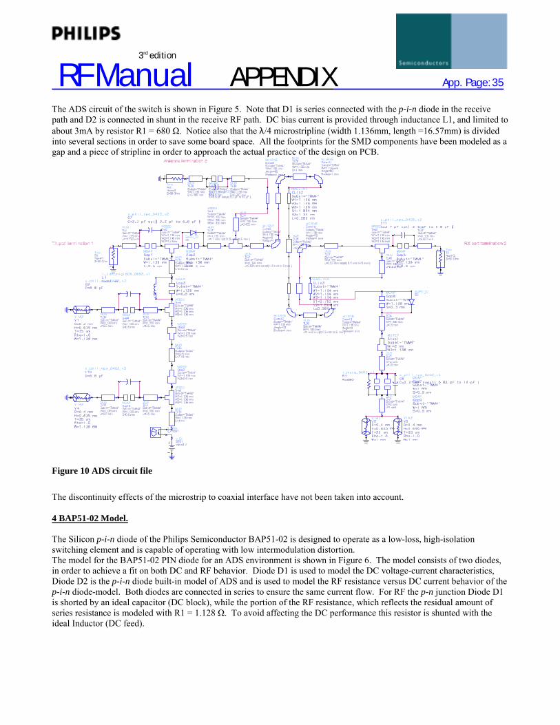
The ADS circuit of the switch is shown in Figure 5. Note that D1 is series connected with the p-i-n diode in the receivepath and D2 is connected in shunt in the receive RF path. DC bias current is provided through inductance L1, and limited toabout 3mA by resistor R1 = 680 Ω. Notice also that the λ/4 microstripline (width 1.136mm, length =16.57mm) is dividedinto several sections in order to save some board space. All the footprints for the SMD components have been modeled as agap and a piece of stripline in order to approach the actual practice of the design on PCB.
Figure 10 ADS circuit file
The discontinuity effects of the microstrip to coaxial interface have not been taken into account.
4 BAP51-02 Model.
The Silicon p-i-n diode of the Philips Semiconductor BAP51-02 is designed to operate as a low-loss, high-isolationswitching element and is capable of operating with low intermodulation distortion.The model for the BAP51-02 PIN diode for an ADS environment is shown in Figure 6. The model consists of two diodes,in order to achieve a fit on both DC and RF behavior. Diode D1 is used to model the DC voltage-current characteristics,Diode D2 is the p-i-n diode built-in model of ADS and is used to model the RF resistance versus DC current behavior of thep-i-n diode-model. Both diodes are connected in series to ensure the same current flow. For RF the p-n junction Diode D1is shorted by an ideal capacitor (DC block), while the portion of the RF resistance, which reflects the residual amount ofseries resistance is modeled with R1 = 1.128 Ω. To avoid affecting the DC performance this resistor is shunted with theideal Inductor (DC feed).

RF Manual APPENDIX App. Page: 36
3rd edition
Capacitance C2 and inductors L2 and L3 reflect package parasitics. The described model is a linear model that emulates theDC and RF properties of the p-i-n diode from 6 MHz up to 6 GHz.
Figure 11; BAP51-02 Small Signal Model for an ADS environment
5 Circuit and Layout Description
The circuit diagram for the switch is shown in figure 7 and the PC board layout is shown in Figure 8. The bill of materialsfor the switch is given in Table2. The PC board used was 0.635mm thick using FR4 material (εr = 4.6). Copper plane onboth sides was 35 µm thick copper and overlaid with 3 µm gold plating. On the test board SMA connectors were used tofeed the RF signals into the board.
C46.8pF
Ant
D2
RX input50 Ω
C54.7pF
TX output50 Ω
C12.2pF
L122nH
C21nF
D1
R1680Ω
C62.2pF
TL1, 50 Ω1.14x12mm
TL2, 50 Ω1.14x7mm
TL3, 50 Ω1.14x16.6mm
TL4, 50 Ω1.14x6mm
C36.8pF
Vs=0/3.7V
Figure 12; circuit diagram Figure 13; PC board Layout.
RF Manual APPENDIX App. Page: 37
3rd edition
Component Value Footprint ManufacturerC1 2.2 pF 0402 PhilipsC2* 1 nF 0402 PhilipsC3 6.8 pF 0402 PhilipsC4 6.8 pF 0402 PhilipsC5 4.7 pF 0402 PhilipsC6 2.2 pF 0402 PhilipsR1 680 Ω 0402 PhilipsD1 BAP51-02 SC79 PhilipsD2 BAP51-02 SC79 PhilipsL1 22 nH 1005 Taiyo yuden
TL1 λ/4;50 Ω on the PCB
Table 2 Bill of materials *C2 is optional.
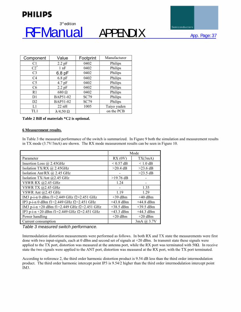
6 Measurement results.
In Table 3 the measured performance of the switch is summarized. In Figure 9 both the simulation and measurement resultsin TX mode (3.7V/3mA) are shown. The RX mode measurement results can be seen in Figure 10.
ModeParameter RX (0V) TX(3mA)Insertion Loss @ 2.45GHz < 0.57 dB < 1.0 dBIsolation TX/RX @ 2.45GHz >20.4 dB >23.6 dBIsolation Ant/RX @ 2.45 GHz - >23.5 dBIsolation TX/Ant @2.45 GHz >19.76 dB -VSWR RX @2.45 GHz 1.24 -VSWR TX @2.45 GHz - 1.35VSWR Ant @2.45 GHz 1.19 1.29IM3 p-i-n 0 dBm f1=2.449 GHz f2=2.451 GHz +39 dBm +40 dBmIP3 p-i-n 0 dBm f1=2.449 GHz f2=2.451 GHz +43.8 dBm +44.8 dBmIM3 p-i-n +20 dBm f1=2.449 GHz f2=2.451 GHz +38.5 dBm +39.5 dBmIP3 p-i-n +20 dBm f1=2.449 GHz f2=2.451 GHz +43.3 dBm +44.3 dBmPower handling +20 dBm +20 dBmCurrent consumption 3mA @ 3.7VTable 3 measured switch performance.
Intermodulation distortion measurements were performed as follows. In both RX and TX state the measurements were firstdone with two input-signals, each at 0 dBm and second set of signals at +20 dBm. In transmit state these signals wereapplied to the TX port, distortion was measured at the antenna port, while the RX port was terminated with 50Ω. In receivestate the two signals were applied to the ANT port, distortion was measured at the RX port, with the TX port terminated.
According to reference 2, the third order harmonic distortion product is 9.54 dB less than the third order intermodulationproduct. The third order harmonic intercept point IP3 is 9.54/2 higher than the third order intermodulation intercept pointIM3.

RF Manual APPENDIX App. Page: 38
3rd edition
Figure 14; Results in TX mode; red curves are measurements, blue curves are the simulated ones.
Remark: Loss and isolation results are all including approximately 0.2 dB loss of the SMA connectors which were used tofed the RF signals through the design. This has a great impact on the insertion loss results.

RF Manual APPENDIX App. Page:39
3rd edition
Figure 15; Results in RX mode; red curves are measurements, blue curves are the simulated ones
Remark: Loss and isolation results are all including approximately 0.2 dB loss of the SMA connectors which were used tofed the RF signals through the design. This has a great impact on the insertion loss results.
Recommendations.
1 In this design the BAP51-02 was used because it’s designed for switching applications related to insertion loss andisolation. When a better IM distortion is required it is better to use the BAP64-02 from Philips Semiconductors.
2 As can be seen the λ/4 section requires a lot of boards space. This section could be replaced by a lumped elementconfiguration, which results offers board real estate savings.
References: 1; Gerald Hiller, “Design with PIN diodes,” App note APN1002 Alpha industries inc.2; Gerald Hiller, “Predict intercept points in PIN diode switches,” Microwaves & RF, Dec. 1985.3; Robert Caverly and Gerald Hiller, “Distortion in PIN diode control circuits,” IEEE Trans onMicrowave

RF Manual APPENDIX App. Page: 40
3rd edition
Appendix D: Application of theRF Switch BF1107/8 Mosfets
APPLICATION OF THE RF SWITCH BF1107INTRODUCTIONIf a (Mos)fet is used in its linear region, it can be used as a variableresistor. The resistance depends on the bias voltage between Gate and Sourceand the pinch - off voltage of the Mosfet.If the bias voltage is lower than the pinch - off voltage the resistance of the Mosfetis infinite. If the bias voltage is much higher than the pinch - off voltage theresistance of the Mosfet is low.Due to this a Mosfet can be used as a switch.At low Gate - Source voltages the Mosfet is switched off and at high Gate -Source voltages the Mosfet is switched on.If a Mosfet is used with relatively low capacitances the Mosfet can be used asan RF switch. With this Rf switch, RF signals can be switched off and on.The BF1107 is a triode Mosfet intended for switching RF signals.If the Drain - Source voltage is set to 0V, this Mosfet is biased in its linear region.This Mosfet has a pinch - off voltage of approx. 3V.Therefore this Mosfet is switched on if the Gate - Source voltage is 0V. Togetherwith a Drain - Source voltage of 0V this means that the Mosfet is switched onif all bias voltages are 0V.If the Gate - Source voltage is set to a value lower than 3V this Mosfet isswitched off.
APPLICATION IN A VIDEO RECORDERA block diagram of the principle circuit of the RF front end of a VCR is given in Fig.1 below.
Wide bandsplitteramplifier
Tuner
PLL /Modulator
Antennainput
Outputto TV set
RF Manual APPENDIX App. Page: 41
3rd edition
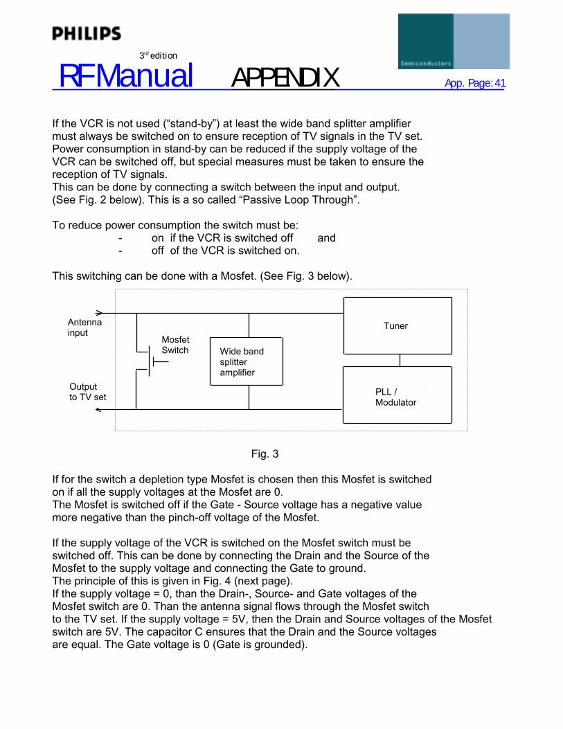
If the VCR is not used (“stand-by”) at least the wide band splitter amplifiermust always be switched on to ensure reception of TV signals in the TV set.Power consumption in stand-by can be reduced if the supply voltage of theVCR can be switched off, but special measures must be taken to ensure thereception of TV signals.This can be done by connecting a switch between the input and output.(See Fig. 2 below). This is a so called “Passive Loop Through”.
To reduce power consumption the switch must be:- on if the VCR is switched off and- off of the VCR is switched on.
This switching can be done with a Mosfet. (See Fig. 3 below).
Fig. 3
If for the switch a depletion type Mosfet is chosen then this Mosfet is switchedon if all the supply voltages at the Mosfet are 0.The Mosfet is switched off if the Gate - Source voltage has a negative valuemore negative than the pinch-off voltage of the Mosfet.
If the supply voltage of the VCR is switched on the Mosfet switch must beswitched off. This can be done by connecting the Drain and the Source of theMosfet to the supply voltage and connecting the Gate to ground.The principle of this is given in Fig. 4 (next page).If the supply voltage = 0, than the Drain-, Source- and Gate voltages of theMosfet switch are 0. Than the antenna signal flows through the Mosfet switchto the TV set. If the supply voltage = 5V, then the Drain and Source voltages of the Mosfetswitch are 5V. The capacitor C ensures that the Drain and the Source voltagesare equal. The Gate voltage is 0 (Gate is grounded).
Wide bandsplitteramplifier
Tuner
PLL /Modulator
Antennainput
Outputto TV set
MosfetSwitch
RF Manual APPENDIX App. Page: 42
3rd edition
Supply voltage =0; VCR is switched off; Mosfet is switched on.Supply voltage =5V; VCR is switched on; Mosfet is switched off.
Wide bandsplitteramplifier
TunerAntennainput
Outputto TV set
MosfetSwitch
PLL /Modulator
C
Then the antenna signal flows through the VCR as usual.
Fig. 4
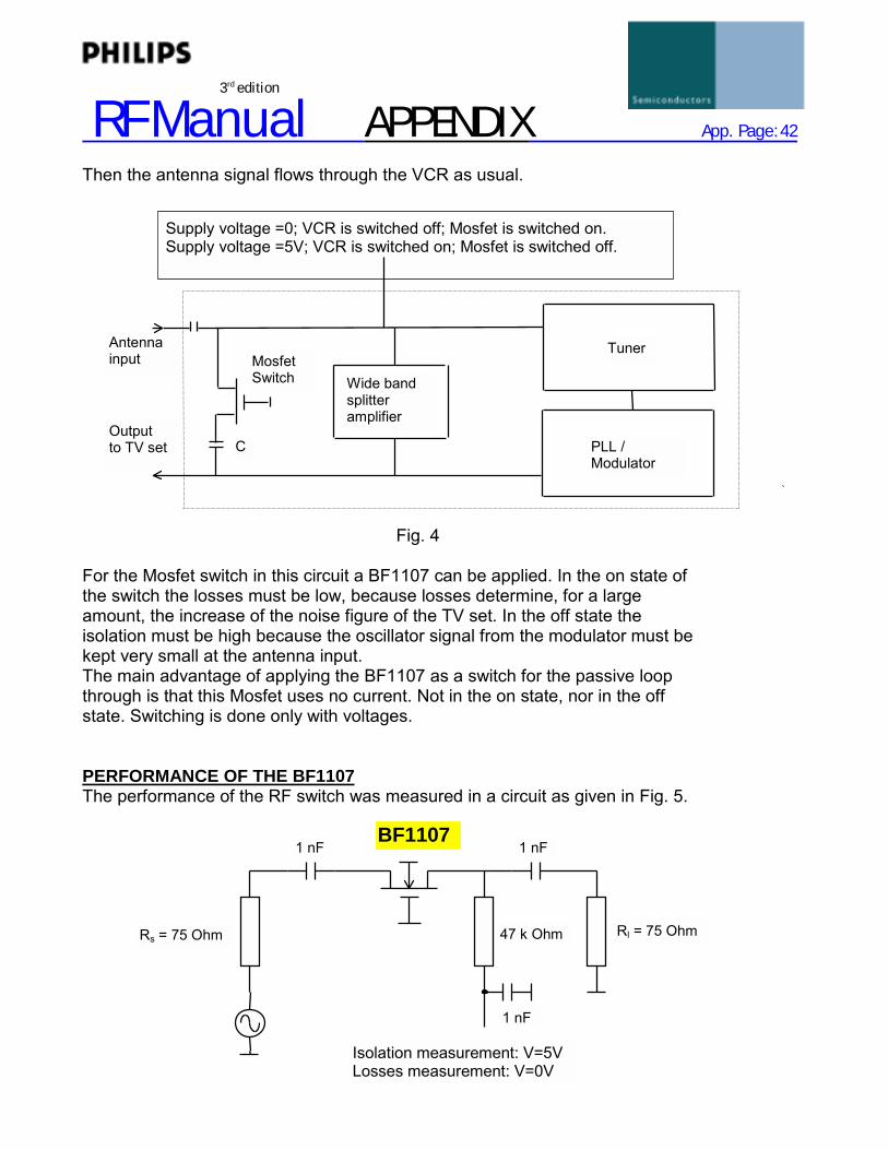
For the Mosfet switch in this circuit a BF1107 can be applied. In the on state ofthe switch the losses must be low, because losses determine, for a largeamount, the increase of the noise figure of the TV set. In the off state theisolation must be high because the oscillator signal from the modulator must bekept very small at the antenna input.The main advantage of applying the BF1107 as a switch for the passive loopthrough is that this Mosfet uses no current. Not in the on state, nor in the offstate. Switching is done only with voltages.
PERFORMANCE OF THE BF1107The performance of the RF switch was measured in a circuit as given in Fig. 5.
1 nF1 nF
Rl = 75 OhmRs = 75 Ohm 47 k Ohm
1 nF
BF1107
Isolation measurement: V=5VLosses measurement: V=0V

RF Manual APPENDIX App. Page: 43
3rd edition
In this circuit we measured isolation and losses as a function of frequency.The results of these measurements are given in Fig. 6.
Losses and isolation of RF switch in testcircuit Rl=Rs=75 Ohm
-12
-10
-8
-6
-4
-2
00 200 400 600 800 1000
frequency (MHz)
Loss
es (d
B)
-60
-50
-40
-30
-20
-10
0
Isol
atio
n (d
B)
losses BF1107isolation BF1107
Fig. 6
The isolation (Mosfet is switched off) in the testcircuit is mainly determined bythe feedback of the Mosfet in common Gate plus the parasitic capacitanceof the testcircuit between Drain and Source. This parasitic capacitance must bevery small.The losses (Mosfet is switched on) in the testcircuit are at low frequenciesdetermined by the RDS on of the Mosfet and at high frequencies by the RDS onand the Drain - Gate and Source - Gate capacitances of the Mosfet.The parasitic capacitances of the circuit must be kept much lower than thecapacitances of the Mosfet.
SPECIAL MEASURES TO BE TAKENIn Fig. 4 only the principle of the application circuit of the switch in the VCR isgiven.In the practical application circuit of a VCR the input and output of the wide bandsplitter amplifier are connected to the input and output of the switch.As stated in chapter 3 the losses in the on situation of the switch are alsodetermined by the capacitances at the input and the output of the switch.If in the principle circuit of Fig.4 the Mosfet is switched on, then the wide band

RF Manual APPENDIX App. Page: 44
3rd edition
splitter amplifier is still connected to the RF switch. This results into higherlosses. Therefore special measures are needed to reduce the influence ofthe presence of the amplifier on the losses.Theoretically this can be done by disconnecting the input as well as the outputof the amplifier from the switch.In practice this disconnecting can be done with a switch.The principle of the circuit is then as given in Fig. 7.
Fig. 7
The losses of the two switches in Fig. 7 must have low resistance if this switchis on and low capacitance if this switch is off. Such switches can be madewith diodes. With the right choice of the diodes the resistance is low if the diodeis forward biased and the capacitance is low if the bias voltage of the diode is 0V.Diodes that can be applied are bandswitching diodes (e.g. BA792 or BA277).If the two stages of the wide band splitter amplifier are biased via the diodeswitches then the amplifier is “disconnected” from the switch if the supply voltageis 0V and “connected” if the supply voltage is 5V.The main part of the circuit is then as given in Fig. 8 next page.
Supply voltage =0; VCR is switched off; Mosfet is switched on.Supply voltage =5V; VCR is switched on; Mosfet is switched off.
Wide bandsplitteramplifier
TunerAntennainput
Outputto TV set
MosfetSwitch
PLL /Modulator
C
switch
switch

RF Manual APPENDIX App. Page: 45
3rd edition
Fig. 8
CONCLUSIONSThe BF1107 is a specially developed triode Mosfet for the application ofRF switch. In the on condition of the switch as well as in the off condition noD.C current flows through the Mosfet.One of the application areas is the “Passive Loop Through” in a VCR.The requirements for this application are:Losses: typ 2dB max. 4dB.Isolation: > 30dB.This can be achieved with a BF1107 in the circuit of Fig. 8.If this switch is applied the supply voltage of the VCR can be switched offin the “stand - by” condition of the VCR.The R.F signal path to the T.V. set is then via the switch and not via a(power consuming) wide band splitter amplifier.
Antennainput
Part of the wide bandsplitter amplifier
PassiveLoopThrough
Supplyvoltage
Supplyvoltage
Supplyvoltage
Outputto TV set
RF Manual APPENDIX App. Page: 46
3rd edition
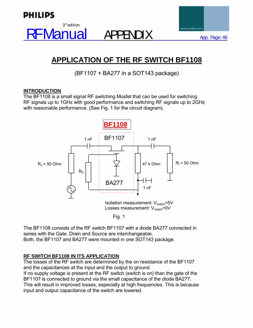
APPLICATION OF THE RF SWITCH BF1108(BF1107 + BA277 in a SOT143 package)
INTRODUCTIONThe BF1108 is a small signal RF switching Mosfet that can be used for switchingRF signals up to 1GHz with good performance and switching RF signals up to 2GHzwith reasonable performance. (See Fig. 1 for the circuit diagram).
Fig. 1
The BF1108 consists of the RF switch BF1107 with a diode BA277 connected inseries with the Gate. Drain and Source are interchangeable.Both, the BF1107 and BA277 were mounted in one SOT143 package.
RF SWITCH BF1108 IN ITS APPLICATIONThe losses of the RF switch are determined by the on resistance of the BF1107and the capacitances at the input and the output to ground.If no supply voltage is present at the RF switch (switch is on) than the gate of theBF1107 is connected to ground via the small capacitance of the diode BA277.This will result in improved losses, especially at high frequencies. This is becauseinput and output capacitance of the switch are lowered.
Rs = 50 Ohm
1 nF1 nF
Rl = 50 Ohm47 k Ohm
Isolation measurement: Vsupply=5VLosses measurement: Vsupply=0V
RD
1 nF
BF1107
BA277
BF1108

RF Manual APPENDIX App. Page: 47
3rd edition
The isolation of the RF switch is determined by its’ off resistance in parallel with thefeedback capacitance and the impedance between gate and ground.If there is a 5V supply voltage present at the switch (switch is off) than the gate of theBF1107 is connected to ground via the small seriesresistance of the BA277.The impedance between gate and ground is mainly determined by the inductancefrom gate to ground, especially at high frequencies. Therefore the small extra seriesresistance of the BA277 will have marginal influence on the isolation of the switch.However, the extra series inductance has influence on the isolation, especially athigh frequencies.For the BF1107 no current is needed as well in the on state as in the off state.For the BF1108 also no current is needed for the on state. In the off state a smallcurrent through the BA277 is needed to ensure relatively low series resistance.
MEASUREMENTS ON THE BF1108On the BF1108 we have measured the losses in the on state (Vsupply = 0V) and theisolation in the off state (Vsupply = 5V) in a 50Ω test circuit (see Fig. 1).For comparison we have also measured the losses and the isolation of a BF1107.The results of the measurements on a BF1107 are given in Graph. 1.The results of the measurements on a BF1108 are given in the Graphs. 2 and 3.In Graph 2 the results are given with a bias resistor (to the BA277) of 4.7kΩ.This is a d.c. forward current through the diode of appr. 1mA.Graph 3 shows the results with a d.c. current through the diode of appr. 2mA.(Bias resistor to the diode 2.2kΩ).In the specification the losses and the isolation are specified up to 860MHz.However, it is possible to use the BF1108 also at higher frequencies with somewhatless performance. For information we have also measured the BF1108 and BF1107 atfrequencies up to 2.05GHz.The results of these measurements are given in Graph 4.
INFLUENCE OF PARASITIC CAPACITANCESIt is obvious that parasitic capacitances will influence the performance of the RFswitch, also, additional feedback as well as additional parallel capacitances inparallel with the BF1108.Measurements are done with additional parallel capacitances between Drain andGround and between Source and Ground (see Fig. 2, next page).We have also added some additional feedback between Drain and Source.The results of these measurements are given in Graph 5.

RF Manual APPENDIX App. Page: 48
3rd edition
Fig. 2
The additional feedback was made by a short wire connected to the Drain, bendingit towards the Source.
We have also done measurements with additional capacitances between Drain andGate and between Source and Gate. Also with additional feedback between Drainand Source. Than the circuit diagram is as given in Fig. 3.
Rs =50 Ohm
47k Ohm
Isolation measurement: Vsupply=5VLosses measurement: Vsupply=0V
1 nF
BF1107
BA277
BF1108
RD
1 nF
0.82 pF
1 nF
Rl =50 Ohm0.82 pF
Isolation measurement: Vsupply=5VLosses measurement: Vsupply=0V
47k Ohm
1 nF
BF1108
RD
Rs =50 Ohm
1 nF
0.82 pF0.82 pF Rl =
50 Ohm
1 nFBF1107
BA277
RF Manual APPENDIX App. Page: 49
3rd edition
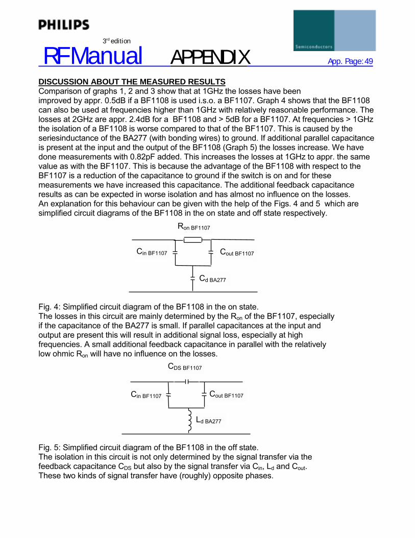
DISCUSSION ABOUT THE MEASURED RESULTSComparison of graphs 1, 2 and 3 show that at 1GHz the losses have beenimproved by appr. 0.5dB if a BF1108 is used i.s.o. a BF1107. Graph 4 shows that the BF1108can also be used at frequencies higher than 1GHz with relatively reasonable performance. Thelosses at 2GHz are appr. 2.4dB for a BF1108 and > 5dB for a BF1107. At frequencies > 1GHzthe isolation of a BF1108 is worse compared to that of the BF1107. This is caused by theseriesinductance of the BA277 (with bonding wires) to ground. If additional parallel capacitanceis present at the input and the output of the BF1108 (Graph 5) the losses increase. We havedone measurements with 0.82pF added. This increases the losses at 1GHz to appr. the samevalue as with the BF1107. This is because the advantage of the BF1108 with respect to theBF1107 is a reduction of the capacitance to ground if the switch is on and for thesemeasurements we have increased this capacitance. The additional feedback capacitanceresults as can be expected in worse isolation and has almost no influence on the losses.An explanation for this behaviour can be given with the help of the Figs. 4 and 5 which aresimplified circuit diagrams of the BF1108 in the on state and off state respectively.
Fig. 4: Simplified circuit diagram of the BF1108 in the on state.The losses in this circuit are mainly determined by the Ron of the BF1107, especiallyif the capacitance of the BA277 is small. If parallel capacitances at the input andoutput are present this will result in additional signal loss, especially at highfrequencies. A small additional feedback capacitance in parallel with the relativelylow ohmic Ron will have no influence on the losses.
Fig. 5: Simplified circuit diagram of the BF1108 in the off state.The isolation in this circuit is not only determined by the signal transfer via thefeedback capacitance CDS but also by the signal transfer via Cin, Ld and Cout.These two kinds of signal transfer have (roughly) opposite phases.
Cout BF1107Cin BF1107
Cd BA277
Ron BF1107
CDS BF1107
Cin BF1107 Cout BF1107
Ld BA277
RF Manual APPENDIX App. Page: 50
3rd edition
If the signal transfer is only determined by the feedback capacitance one wouldexpect a decrease in the isolation with 6dB / octave (if 1/ωCDS << (Rs + Rl).However, due to the opposite phases of the two signal transfers there will be a dipin the graph for the isolation as a function of frequency. In the Graphs 2, 3, 4 and 5 this dip ispresent at about 950MHz if no additional feedback is present. If additional feedback is presentthe dip shifts to a higher frequency. More series inductance in the Gate shifts the dip to a lowerfrequency. This can be seen from Graph 4 where the BF1107 and BF1108 are compared.For the BF1107 the dip is present at appr. 1850 MHz. The BF1108 shows a dip atappr. 950MHz. Due to this the isolation of the BF1108, compared to that of theBF1107, is worse at frequencies > 1GHz..
If additional capacitance (0.82pF) is present between Drain and Gate and Sourceand Gate, then the losses increase by appr. 0.25dB at 1GHz. This can also be explained fromthe fact that the capacitive signal path to ground is lower ohmic than without this additionalcapacitance. The influence of additional capacitances is much lower than connecting themdirectly to ground. This is because of the presence of the small diode capacitance. The isolationas a function of frequency is very dependent on the presence of the additional capacitances.(Compare Graph 3 and 6). We see that the dip in the curve is shifted to appr. 650MHz. Andnow the isolation at 1GHz is worse than 30dB. As stated before the dip can be shifted to ahigher frequency if additional feedback is present. Than the dip can again be set to appr.950MHz. The isolation at lower frequencies is than worsened, but now at 1GHz an isolation of> 30dB can be achieved (see Graph 6). Additional feedback does not influence the losses.
CONCLUSIONSThe BF1108 is an RF switch which has low losses at frequencies up to 2GHz.In the on state the losses are 1.15dB typical at 50MHz slowly increasing to1.4dB typical at 1GHz and 2.4dB typical at 2GHz. The losses are strongly dependent onadditional parallel capacitances present at the input and the output of the switch and almost notdependent on additional feedback between Drain and Source. The isolation of the BF1108 is >50dB at 50MHz decreasing to appr. 35dB typical at 1GHz and appr. 15dB typical at 2GHz.The Graphs for the isolation as a function of frequency show a dip at a certain frequency. Thisdip is caused by a compensation effect of a signal transfer via the Drain - Source feedbackcapacitance and a signal transfer via the input- and output capacitances and the seriesinductance in the Gate. These two signal transfers have opposite phase which causes the dipin the curve. From this we can also conclude that the losses are strongly dependent on thefeedback capacitance, the Drain - Gate and the Source - Gate capacitances and the seriesinductance in the Gate. Additional feedback capacitance shifts the dip in the curve isolation as afunction of frequency to a higher frequency. The isolation at low frequencies is than worsened.Additional capacitances between Drain and Gate and Source and Gate and moreseries inductance in the Gate shifts the dip to lower frequencies.

RF Manual APPENDIX App. Page: 51
3rd edition
Appendix E: Application Note MOSFET1. INTRODUCTION
At Philips we have different types of Dual Gate MOSFETs.Our preferred types for use in television tuners are:
the 12V types in SOT143: BF998, BF908,BF1100in SOT143R: BF998R, BF908R,BF1100R
in SOT343R: BF998WR, BF908WR,BF1100WR
the 9V types in SOT143: BF1100, BF1109in SOT143R: BF1100R, BF1109Rin SOT343R: BF1100WR, BF1109WR
and also for 9V the BF998, BF998R, BF998WR,BF908, BF908R and BF908WR
with somewhat worse performance compared to the 12V application.
and the 5V types in SOT143: BF904, BF904A, BF909, BF909A, BF1101, BF1105, BF1201, BF1202
in SOT143R: BF904R, BF904AR, BF909R, BF909AR, BF1101R, BF1105R, BF1201R, BF1202R
in SOT343R BF904WR, BF904AWR, BF909WR, BF909AWR BF1101WR, BF1105WR, BF1201WR, BF1202WR andthe 2 in 1 MOSFETs in SOT363: BF1102, BF1102R, BF1203, BF1204
The types BF998((W)R) and BF908((W)R) have no integrated bias.The types BF904((W)R), BF909((W)R), BF1100((W)R), BF1101((W)R), BF1201((W)R),BF1202((W)R), BF1102(R), BF1203 and BF1204 have partly integrated bias.The types BF1105((W)R), and BF1109((W)R), have fully integrated bias.As a consequence the external bias circuits of the different MOSFETs are different.The BF998((W)R) and the BF904((W)R) are MOSFETs with relatively low transconductance (Yfs typ ~ 24 -25 mS) and capacitances (Cis typ: 2.1 - 2.2 pF). The BF908((W)R) and the BF909((W)R), BF1102(R) areMOSFETs with relatively high transconductance (Yfs typ ~ 43 mS) and capacitances (Cis typ ~ 3.1 - 3.6 pF).The BF1100((W)R), BF1101((W)R), BF1105((W)R) and BF1109((W)R), are MOSFETs with atransconductance between the above mentioned values (Yfs typ ~ 28 - 31 mS) and still has low capacitances(Cis typ ~ 2.2 pF). The MOSFETs were developed with different transferconductances to optimize them fordifferent frequency ranges.The BF1201((W)R), (Yfs typ ~ 28mS; Cis typ ~ 2.6 pF) and BF1202((W)R), (Yfs typ ~30mS; Cis typ ~ 1.7 pF) had been especially developed for improved cross-modulation and improved slope ofthe AGC characteristics.
2. Dual Devices in Single PackagesThe (2-in-1 MOSFET) BF1102 is a combination of two BF909s with shared source and gate 2 leads. The(2-in-1 MOSFET) BF1203 is a combination of BF1201 and BF1202 with shared source and gate 2 leads.The (2-in-1 MOSFET) BF1204 is a combination of 2 x BF1202 with shared source and gate 2 leads.

RF Manual APPENDIX App. Page: 52
3rd edition
3. GENERALIn the introduction all the type numbers and the different packages are mentioned. The package has noinfluence on the DC biasing. The influence of the package on the RF parameters (in the frequency area oftelevision tuners) is small. Therefore in this report the application differences and examples will be given forthe devices in the SOT143 package. This application information is also valid for the MOSFETs in SOT143R,SOT343R and SOT363.
4. DC BIAS CIRCUITSDC bias circuits for MOSFETs without integrated bias.We have two basic types of MOSFETs without integrated bias, BF908 and BF998. These MOSFETs aredepletion types. Depletion type MOSFETs have negative pinch-off voltages. In TV tuners AGC is necessary.For TV tuners no negative AGC voltaes are available. Due to this lack of negative voltage it is necessary to liftup the source voltage. Otherwise it is not possible to obtain maximum possible gain reduction. This lift upmust be done with two resistors in the device source. For AC these resistors must be decoupled with acapacitor. The nominal current of the BF998 is 10mA and that of the BF908 is 15mA. This biasing is donewith a voltage divider at Gate1. Because there is no Gate1 current in the MOSFETs the values of the resistorsof the Gate1 voltage divider need to be only relatively high resistance. The parallel connection of the 2 esistorsshould be higher than 10kΩ. The DC circuit for biasing the MOSFETs without integrated bias is then asshown in Fig. 1 below.
Fig.1: Principle of the bias circuit for MOSFETs without integrated bias.
As stated in the introduction the BF998 and BF908 are for 12V tuners. However, they can be applied at 9V withsome loss of performance. For the 12V and 9V application the values of the resistors R1, R2, R3 and R4 can becalculated. At 12V application we assume that the nominal AGC voltage is 9V. In the 9V application the nominal
G
G
1
2
D
S
Out
Vsupply
Vsupply
In
VsupplyV
agc
BF998, BF908
R1 R2R R3 4

RF Manual APPENDIX App. Page: 53
3rd edition
AGC voltage is 7.5V. The nominal VG2-S in the 12V - as well as in the 9V application is 4V. In Table 1 below, thevalues of the resistors for the 12V- and 9V applications of the BF998 and BF908 are given.
Table 1: Resistors in the bias circuit for MOSFETs without integrated bias.Vsupply Vagc nom VG2-S nom ID nom R1 / R2 R3 (Ω) R4 (Ω)
BF998 12 V 9 V 4 V 10 mA 5 / 7 360 1800BF998 9 V 7.5 V 4.V 10 mA 7 / 11 240 1200BF908 12 V 9V 4 V 15 mA 5 / 7 240 1200BF908 9 V 7.5 V 4 V 15 mA 7 / 11 160 750
DC bias circuit of MOSFETs with partly integrated bias.We have nine types of MOSFETs with partly integrated bias. The 5V types BF904, BF909, BF1101,BF1102, BF1201, BF1202, BF1203 and BF1204 and the 9V to 12V type BF1100. These MOSFETs areenhancement types. This term means that the pinch-off voltages are positive. No negative voltages areneeded for fully switching-off the MOSFETs. Due to this it is not necessary to lift up the Source voltage. Forapplications of these types the nominal Gate2 voltage is set to 4V.In 12V applications the nominal AGC voltage is 9V. In a 9V application the nominal AGC voltage is 7.5V.For these applications a voltage divider at Gate2 is needed. Because there is no Gate2 current, no specialrequirements for this divider are necessary. We propose to set the nominal current of the BF904 and BF1100at 10mA. That of the BF909, BF1102 and BF1201 at 15mA and that of the BF1101 and BF1202 at 12mA. Inthe BF1203 we propose to bias the BF1203a at 15mA. We propose to bias the BF1203b, in the BF1203, at12mA. In the BF1204, we propose to bias both MOSFETs, BF1204a and BF1204b at 12mA. This biasing isdone with a resistor (RGG) at Gate1.
The principle of the DC circuit biasing for MOSFETs with partly integrated bias is as given in Figures 2 and 3(next page).
Note: In Figures 2 and 3 the basic principles of the circuit are given. There is no information about the pin-outs of the different MOSFETs. The pinning of the BF1204 is different from that of the BF1102 and BF1203.
The necessary resistors for the different applications are given in Table 2 (page 5).

RF Manual APPENDIX App. Page: 54
3rd edition
Figure 2: Basic bias circuit for single MOSFETs with partly integrated bias.
Figure 3: Basic bias circuit for dual MOSFETs with partly integrated bias.
G
G
1
2
D
S
Out
Vsupply
In
VsupplyVagc
BF1100, BF1101
RGG
R1
R2
BF904, BF909
BF1201, BF1202
G
G
1
2
D
S
Out
Vsupply
In
Vsupply
Vagc
BF1102
RGGb
R2
BF1203, BF1204
Inb
G1b
a
RGGa
DOut
Vsupply
Vsupply
b
a

RF Manual APPENDIX App. Page: 55
3rd edition
Table 2: Resistors in the bias circuit for MOSFETs with partly integrated bias.Application Proposed ID RGG R1 / R2
BF904 5 V 10 mA 120 kΩ no R1
BF909 5 V 15 mA 120 kΩ no R1
BF1101 5 V 12 mA 120 kΩ no R1
9 V 12 mA 180 kΩ 8 / 7BF1100 12 V 12 mA 250 kΩ 4 / 5BF1201 5 V 15 mA 62 kΩ no R1
BF1202 5 V 12 mA 120 kΩ no R1
BF1102 (1) 5 V 15 mA 120 kΩ no R1
BF1102 (2) 5 V 15 mA 120 kΩ no R1
BF1203a 5 V 15 mA 62 kΩ no R1
BF1203b 5 V 12 mA 120 kΩ no R1
BF1204a 5 V 12 mA 120 kΩ no R1
BF1204b 5 V 12 mA 120 kΩ no R1
DC bias circuit of MOSFETs with fully integrated bias.We have two types of MOSFETs with fully integrated bias. The 5V type BF1105 and the 9V type
BF1109. These MOSFETs are also enhancement types and therefore no negative voltages are needed forfully switching-off theMOSFETs. Due to this it is not necessary to raise the source voltage above ground reference. Because of thefullyintegrated bias no external resistor at Gate1 is needed for biasing the MOSFETs. Both types, BF1105 andBF1109,have been developed for a typical “Self Biasing Current” of 12mA.
For application of these types the nominal Gate2-Source voltage is to be set to 4V. In 5V applicationsthe nominalAGC voltage is 4V. In a 9V application the nominal AGC voltage is 7.5V. For the 9V application a voltagedivider atGate2 is needed. Because there is no Gate2 current, no special requirements for this divider are necessary.The DCcircuit for biasing the MOSFETs with fully integrated bias is shown in Figure 4 (next page).
The necessary resistors for the different applications are provided in Table 3 (below).
Table 3: Resistors in the bias circuit for MOSFETs with fully integrated bias.
ApplicationTypical
“Self biasing current”R1 / R2
BF1105 5 V 12 mA no R1
BF1109 9 V 12 mA 8 / 7
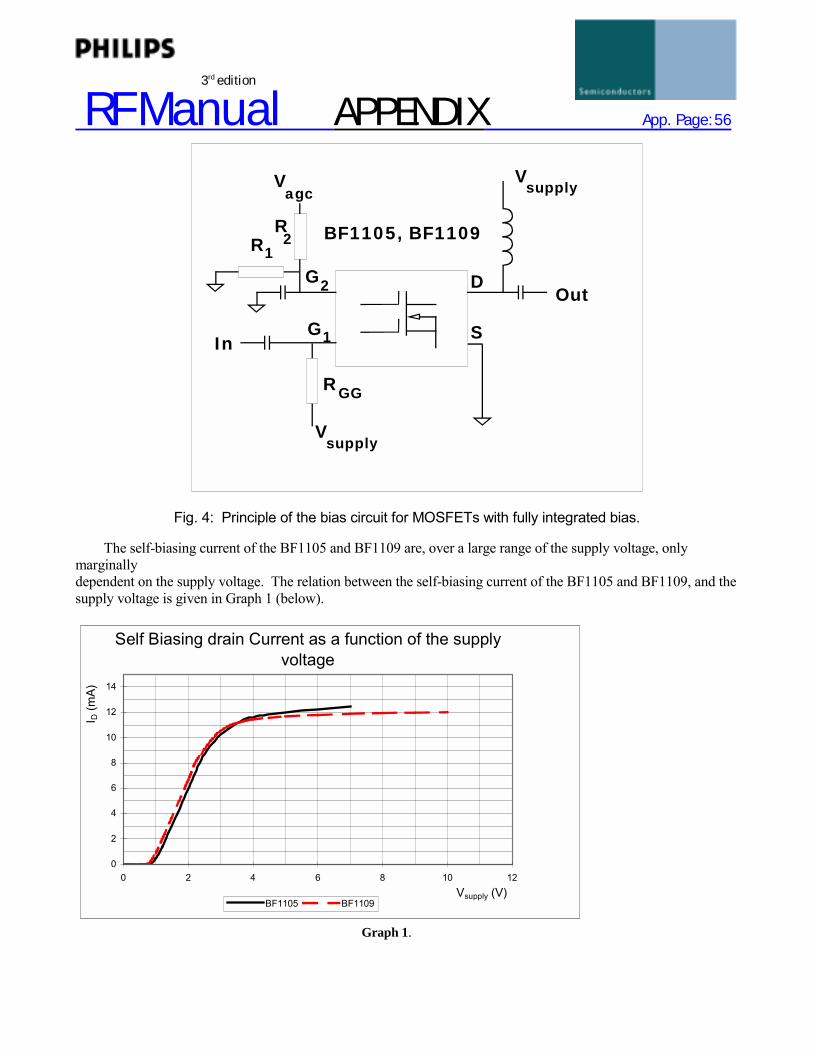
RF Manual APPENDIX App. Page: 56
3rd edition
Fig. 4: Principle of the bias circuit for MOSFETs with fully integrated bias.
The self-biasing current of the BF1105 and BF1109 are, over a large range of the supply voltage, onlymarginallydependent on the supply voltage. The relation between the self-biasing current of the BF1105 and BF1109, and thesupply voltage is given in Graph 1 (below).
Self Biasing drain Current as a function of the supply voltage
0
2
4
6
8
10
12
14
0 2 4 6 8 10 12Vsupply (V)
I D (m
A)
BF1105 BF1109
Graph 1.
G2 D
S
Out
Vsupply
In
VsupplyV
agc
BF1105, BF1109
RGG
R1
R2
G1
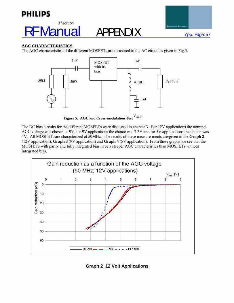
RF Manual APPENDIX App. Page: 57
3rd edition
AGC CHARACTERISTICSThe AGC characteristics of the different MOSFETs are measured in the AC circuit as given in Fig.5.
Figure 5: AGC and Cross-modulation Test Circuit
The DC bias circuits for the different MOSFETs were discussed in chapter 3. For 12V applications the nominalAGC voltage was chosen as 9V, for 9V applications the choice was 7.5V and for 5V appli-cations the choice was4V. All MOSFETs are characterized at 50MHz. The results of these measure-ments are given in the Graph 2(12V application), Graph 3 (9V application) and Graph 4 (5V application). From these graphs we see that theMOSFETs with partly and fully integrated bias have a steeper AGC characteristics than MOSFETs withoutintegrated bias.
Graph 2 12 Volt Applications
MOSFETwith itsbias
1nF
1nF1nF
4.7µH RL=50Ω50Ω 50Ω
Vsupply
Gain reduction as a function of the AGC voltage
(50 MHz; 12V applications)
0
10
20
30
40
50
60
0 1 2 3 4 5 6 7 8 9Vagc (V)
Gai
n re
duct
ion
(dB)
BF998 BF908 BF1100

RF Manual APPENDIX App. Page: 58
3rd edition
Graph 3 9 Volt Applications
Graph 4 5 Volt Applications
From Graph 4 we see clearly the improvement of the AGC characteristics of the BF1201, (BF1203a) and theBF1202, (BF1203b and BF1204), especially the BF1201 (BF1203a).
Gain reduction as a function of the AGC voltage(50MHz; 5V applications)
0
10
20
30
40
50
60
0 0.5 1 1.5 2 2.5 3 3.5 4Vagc (V)
Gai
n re
duct
ion
(dB)
BF904 BF909, BF1102 BF1101BF1105 BF1201, BF1203a BF1202, BF1203b, BF1204
Gain reduction as a function of the AGC voltage
(50MHz; 9V applications)
0
10
20
30
40
50
60
0 1 2 3 4 5 6 7 8Vagc (V)
Gai
n re
duct
ion
(dB)
BF998 BF908 BF1100 BF1109

RF Manual APPENDIX App. Page: 59
3rd edition
5. CROSS-MODULATION PERFORMANCEThe cross-modulation performance was measured in a circuit of the basics of which are given in Figure 5. Theresults of the cross-modulation measurements in the circuit of Fig.5 are given in the Graphs 5, 6, and 7. Graph 5shows the cross-modulation performance of the MOSFETs without integrated bias.
Graph 5
The difference in the curves of the BF998 and BF908 (at gain reduction > 40dB) is caused by internalcapacitances. Internal capacitances of the BF908 are higher than that of the BF998. Due to this the cross-modulation performance after 40 dB gain reduction is increased.
Note: Series inductance in the Source has the same effect as increasing the internal capacitances.
The difference in the performance at 12V and 9V supply voltages are caused by the difference in effectiveSource resistor. Due to this effective Source resistor the Gate1 - Source voltage increases (during AGC) 3V in a12V application and only 2V in a 9V application. The higher this voltage-increase, the better the cross-modulation performance.
Graph 6 (next page) shows the cross-modulation performance of the MOSFETs with partly integrated bias. Thedifferences we see here are caused by the different increase of the Gate1 - Source voltage during AGC, caused bythe different supply voltages. For the MOSFETs in a 5V application the Gate1 - Source voltage at maximum gainreduction is 5V. For the BF1100 the Gate1 - Source voltage at maximum gain reduction is 9V in a 9V applicationand 12V in a 12V application. The BF1201 (BF1203a) and BF1202 (BF1203b and BF1204), are especiallydeveloped for improved cross modulation. This can clearly been seen from the characteristics.
Cross modulation as a function of gain reduction(MOSFETs without integrated bias)
80
85
90
95
100
105
0 5 10 15 20 25 30 35 40 45 50Gain reduction (dB)
Uun
w fo
r k=1
% (d
BµV
)
BF998 (12V) BF998 (9V) BF908 (12V) BF908 (9V)

RF Manual APPENDIX App. Page: 60
3rd edition
Graph 6
Graph 7
Cross modulation as a function of gain reduction(MOSFETs with partly integrated bias)
80
85
90
95
100
105
110
115
120
0 10 20 30 40 50Gain reduction (dB)
Uun
w fo
r k=1
% (d
B µV)
BF904 (5V) BF909, BF1102 (5V) BF1100 (12V)BF1100 (9V) BF1101 (5V) BF1201, BF1203a (5V)BF1202, BF1203b, BF1204 (5V)
Cross modulation as a function of gain reduction(MOSFETs with fully integrated bias)
80
85
90
95
100
105
110
115
0 10 20 30 40 50
Gain reduction (dB)
Uun
w fo
r k=1
% (d
BµV
)
BF1105 (5V) BF1109 (9V)

RF Manual APPENDIX App. Page: 61
3rd edition
CONCLUSIONSFor the modern 9V and 5V applications we recommend the use the MOSFETs with partly and fullyintegrated bias.This allows fewer external components for biasing. The advantage of MOSFETs with partly integrated bias is thatthese devices can be used at different voltages and different drain currents. The BF1100 can be applied at supplyvoltages between 9V and 12V. All 5V MOSFETs with partly integrated bias can be applied at supply voltagesbetween 3V and 7V.
It must be taken into account that if the supply voltage is chosen below 5V, the nominal AGC voltage should bechosen at least 0.5V lower than the supply voltage.
The advantage of MOSFETs with fully integrated bias is that the “self biasing” current over a relatively large rangeof the supply voltage is almost independent on this supply voltage.
The slope of the AGC characteristics of the BF1201 (BF1203a) and BF1202 (BF1203b and BF1204) is much lesssteep than that of the other partly- or fully-internally biased MOSFETs. The cross modulation performance of theBF1201 (BF1203a) and BF1202 (BF1203b and BF1204) is much better than that of the other 5V MOSFETs,especially in the region between 10dB and 30dB gain reduction.

RF Manual APPENDIX App. Page: 62
3rd edition
Appendix F: Application noteWCDMA appl.: BGA6589 Wideband Amplifier
1.0 Introduction.This application note provides information that issupplementary to the data sheet for the BGA6589amplifier, and includes temperature and DC stabilitycharacteristics and WCDMA information.
Figure 1 shows the biasing method. The device ismatched to 50 ohms.
Figure 1. Bias Method.
2.0. DC Characteristics.Figure 2 shows the DC load line characteristics of thedevice, when biased with two different voltage andresistor combinations.
0
20
40
60
80
100
120
140
160
0 1 2 3 4 5 6 7 8 9 10 11 12
Voltage at Device Output, VDC
Cur
rent
, mA
-10 C
25 C
90 C0
0
0
Vcc=12V, R=85 ohms
Vcc=8V,R=37 ohms
Figure 2. BGA6589 DC Characteristics.
Reviewing the graphical load line method, we superimposethe equation for the load resistor onto the devicecharacteristics, and the intersection shows the current and thevoltage of the device. The equation for the resistor isbasically a horizontally flipped version of a straight linerepresenting a resistor across a voltage source, which ofcourse runs through the origin and has a slope determined byR and V.
Using BJT terminology, the device voltage at the output pinis VCE. and the supply is VCC.Then,
CCCCE RiVv −= and
RvI
Rv
RVi CE
OCECC
C −=−=
where Io is the intercept on the y axis.
Figure 3 shows the same data expanded. We can see thatwhen biasing with 8V and 37 ohms, the current is stable overtemperature from 82 to 89 mA.

RF Manual APPENDIX App. Page: 63
3rd edition
75
80
85
90
95
4.4 4.6 4.8 5 5.2 5.4Voltage at Device Output, VDC
Cur
rent
, mA -10 C
25 C
90 C0
0
0
Vcc=12V, R=85 ohms
Vcc=8V,
Figure 3. DC Characteristics Expanded
Device variations, however small, and supply voltagevariations are not yet accounted for in the figure.However, when we look at how the device functionsat different currents, we see that IC is not critical. Forexample, in Figure 4 we see that the gain is virtuallyindependent of the bias current.
14
15
16
17
18
19
20
21
22
23
24
50 60 70 80 90 100 110Device Current, mA DC
Gai
n, d
B
900 MHz
1960 MHz
2140 MHz
Figure 4. Gain Stability with Bias.
Similarly, the gain vs. temperature is shown in Figure5. There is a slight negative temperature coefficient.
15
16
17
18
19
20
21
22
23
0 20 40 60 80 100Temperature, Degrees C
Gai
n, d
B
900 MHz
1960 MHz
2140 MHz
Figure 5. Gain Stability with Temperature.

RF Manual APPENDIX App. Page: 64
3rd edition
3.0. WCDMA Performance.
3.1. Normal Bias. Figure 6 shows the spectrum forWCDMA 3GPP, with 15 channels of data. Thefrequency limits for measurement are shown by thearrows for the reference (on) channel and the adjacentchannel. The channel powers are integrated over a 3.84MHz band, with a channel offset of 5 MHz for the ACPmeasurement.
Figure 6. WCDMA Spectrum.
Figure 7 shows the 5 and 10 MHz offset measurementsover a power range. There are many parameters thataffect the ACP, even for the same number of channelsand their allocations, such as the data type (random orrepeating), the powers in the channels (equal ordifferent), pilot length, timing sequence, and the symbolrate.
-70
-65
-60
-55
-50
-45
-40
-35
-30
0 2 4 6 8 10 12 14 16Power Out, dBm
AC
P, d
Bc
2140 MHz. 1 carrier, 15 channels. Integrated BW Method. 85 mA.
5 MHz Offset
10 MHz Offset
The effect of the number of data channels in the WCDMAsignal is shown in Figure 8.
-60
-55
-50
-45
-40
-35
4 6 8 10 12 14 16Power Out, dBm
AC
P, d
Bc
at 5
MH
z O
ffset
WCDMA, 2140 MHz. 1 carrier, 85 mA.
4 channels
15 channels
8 channels(center line)
Figure 8. Effect of Number of Data Channels.
3.2. Reduced Bias. The compression point (P1dB) is affectedby the device current, as expected. The effect of the currentand the associated P1dB on the WCDMA performance isshown in Figure 9. At low powers, the device can tolerate alower current and still stay within acceptable limits. At +12dBm, the bias can drop to 75 mA without undue degradation.

RF Manual APPENDIX App. Page: 65
3rd edition
-55
-50
-45
-40
-35
-30
50 60 70 80 90 100 110Device Current, mA DC
AC
P @
5 M
Hz
Offs
et, d
Bc
+10 dBm
+12 dBm
+14 dBm
2140 MHz, 1 carrier, 15 channels. 85 mA.
Figure 9. ACP with Reduced Bias.
4.1. CCDF. In WCDMA systems (and IS95 systemsand QAM systems in general), the peak to average ratioof the signal can be 12 dB or more. In an amplifierapplication, designing in enough headroom to handle allthe peaks would make it unnecessarily expensive andinefficient. The highest peaks only occur a smallportion of the time (such as parts per million), and canbe allowed to compress in the amplifier. The trade-offis of course distortion and ACP.
A complementary cumulative density function (CCDF)curve is shown in Figure 10 for 32 data channels.Consider first the CCDF for the case of no clipping. Asa very rough thumbnail estimate of ACP, we know fromanalysis that limiting or clipping of events that happen.01% of the time can cause ACP’s in the general rangeof –40 dBc. This of course is dependent on manyfactors, such as type of limiting (hard clipping vs. softcompression, etc.). The value of –40 dBc correspondsto 10 log (.0001), where .0001 is simply .01% as afraction.
CCDF with Clipping
0.0001
0.001
0.01
0.1
1
10
100
0 1 2 3 4 5 6 7 8 9 10 11 12 13
Peak to Average Power, dBPr
obab
ility
, %
32 Channel WCDMA. Pilot, Sync, and Paging Active
60% clip
80% clip
No Clipping
Hard clipping at 8 dB
Figure 10. CCDF.
4.2. Digital Hard Clipping. In the physical layer ofWCDMA systems, advantage can be taken of the high level ofredundancy in the coding, spreading, and overhead bits of thebasic channel data by eliminating some of the symbols beforeentering the amplifier/transmitter. The air interface is designedto operate with fading, dropouts, static etc., therefore,eliminating some small percentage of the symbols can betolerated, because the bulk of these symbols are corrected forin the receive decoding process.
In the basestation, this clipping is done on the digitalsummation of all the I and Q samples, before filtering. This iscritical. This way, the ACP energy caused by the clipping canbe filtered out in the baseband filters before amplification. Thefiltering process softens up the CCDF curve that wouldotherwise be a hard clip, an example of which is shown inFigure 10.
Also in Figure 10, the CCDF is shown for the cases of clippingthe signal at 60% and 80% relative to the highest peak,followed by filtering. While this may seem to be a severeamount of clipping, the highest peaks (uncommon as they are)might actually be 14 dB or more above the average power, sothe more typical peaks of 10 dB or so are not clipped verymuch.

RF Manual APPENDIX App. Page: 66
3rd edition
-60
-55
-50
-45
-40
-35
4 6 8 10 12 14 16Power Out, dBm
AC
P, d
Bc
at 5
MH
z O
ffset
2140 MHz. 1 carrier, 15 channels. 85 mA.
60% clip
80% clip
100% clip(no clip)
Figure 11. Clipping effects on the ACP.
0.0001
0.001
0.01
0.1
1
10
100
0 1 2 3 4 5 6 7 8 9 10 11 12 13 14Peak to Average Power Ratio, dB
Prob
abili
ty, %
Pilot, Sync, and Paging Active
8 channels
15 ch32
4
The effect of clipping on the ACP is shown in Figure11, for a 15 channel WCDMA signal. This is measureddata for the BGA6589. The x axis is average power.
For 32 channels, the ACP is very similar, because the CCDFsare similar, as shown in Figure 12.
5.0. Load Pull.
Class A devices are not often subjected to a load pull test, butdoing so shows the resiliency of the device when the BGA6589is feeding a stage with a less than perfect S11. Figure 13shows the ACP under various VSWR conditions.
-60
-55
-50
-45
-40
-35
-30
-25
-20
0 0.2 0.4 0.6 0.8 1Reflection Coefficient (Unitless)
AC
P, d
Bc
2140 MHz, 1 carrier, 15 channels. 85 mA.
+ 6 dBm
+8 dBm
+10 dBm+12 dBm
+14 dBm
VSWR = 14 dB 7.9 dB 4.4 dB 1.9 dB
Figure 13. Load Pull Test.
For this test, the worst of four phases of reflection was plottedfor a given reflection coefficient, at several powers. TheVSWR corresponding to the reflection coefficient is shown justabove the x axis. At low/medium powers, a significantly“poor” load reflection is tolerable, before degrading the ACP.For each measurement, the gain necessarily changed due to theloading, and the input drive was changed accordingly to keepthe output power constant.
____________________________________BGA6589 Sep 2002 bja