PGA26E19BA-SWEVB008 Half Bridge Evaluation Board€¦ · PGA26E19BA-SWEVB008 Half Bridge Evaluation...
32
PGA26E19BA-SWEVB008 Ver. 1.5 PGA26E19BA-SWEVB008 Half Bridge Evaluation Board consisting: 1. PGA26E19BA 600V 140mΩ X-GaN Power Transistor 2. AN34092B Single channel X-GaN Gate Driver IC 3. General Purpose Half Bridge Isolator The products and product specifications described in the document are subject to change without notice for modification and/or improvement. At the final stage of your design, purchasing, or use of the products, please request for the up- to-date Product Standards in advance to ensure that the latest specifications meet your requirements. Panasonic Semiconductor Solutions Co. Ltd. 1 Kotari-yakemachi, Nagaokakyo, Kyoto 617-8520, Japan http://www.semicon.panasonic.co.jp/en/
Transcript of PGA26E19BA-SWEVB008 Half Bridge Evaluation Board€¦ · PGA26E19BA-SWEVB008 Half Bridge Evaluation...

PGA26E19BA-SWEVB008 Ver. 1.5
PGA26E19BA-SWEVB008 Half Bridge Evaluation Board consisting:
1. PGA26E19BA 600V 140mΩ X-GaN Power Transistor 2. AN34092B Single channel X-GaN Gate Driver IC 3. General Purpose Half Bridge Isolator
The products and product specifications described in the
document are subject to change without notice for modification and/or improvement. At the final stage of your design, purchasing, or use of the products, please request for the up-
to-date Product Standards in advance to ensure that the latest specifications meet your requirements.
Panasonic Semiconductor Solutions Co. Ltd. 1 Kotari-yakemachi, Nagaokakyo, Kyoto 617-8520, Japan http://www.semicon.panasonic.co.jp/en/

PGA26E19BA-SWEVB008 Ver. 1.5 2
Contents
Features ...................................................................................................................................................... 3
Description of the Evaluation board ............................................................................................................. 4
Recommended Operating Conditions .......................................................................................................... 5
Schematic Diagram ...................................................................................................................................... 6
- Schematic Diagram of optional parts...................................................................................................... 7
Bill of Materials............................................................................................................................................ 8
PCB Layout .................................................................................................................................................10
Test circuits ................................................................................................................................................11
- Slew rate test circuit .............................................................................................................................11
- Switching loss test circuit ......................................................................................................................12
- Dead time circuit ..................................................................................................................................12
- Efficiency test circuit .............................................................................................................................13
Equipment ..................................................................................................................................................14
Measurement Procedures ..........................................................................................................................15
Low Side dV/dT test ....................................................................................................................................18
High Side dV/dT test ...................................................................................................................................20
Low Side Switching Loss test .......................................................................................................................22
Efficiency test .............................................................................................................................................24
Thermal Profile ...........................................................................................................................................25
Thermal Cooling..........................................................................................................................................26
Single Input Schematic Diagram ..................................................................................................................27
Single Input Low Side dV/dT test .................................................................................................................28
Single Input Efficiency test ..........................................................................................................................29
Important Notice ........................................................................................................................................30

PGA26E19BA-SWEVB008 Ver. 1.5 3
Features
Figure 1A: PGA26E19BA-SWEVB008 Board Photo
X-GaN Transistor
Blocking Voltage: 600V
Pulse Peak IDS: 23A
IDS (cont): 15A
RDS(on) typ: 140mΩ
Normally Off Device
X-GaN Gate Driver
Supports high switching frequency (~4MHz)
Achieved safe operation by negative voltage
source and active miller clamp
Facilitate gate drive design with high
precision gate current source
Source2Source1
Source
Drain
Gate
PGA26E19BA
AN34092B
Propagation Delay 30ns
D D D D
G S1 S2 S2
S2
High side Iso DCDC Power
JP1
IC1
IC2
QB
QA
DBS
Shunt Resistor
TPS1 TPS2 SMA2
IC5
Low side Iso DCDC Power
Semi Rigid Connector
TPVO
AUXH+ AUXH-
VDD IN_H
GND EN GND IN_L
AUXL- AUXL+

PGA26E19BA-SWEVB008 Ver. 1.5 4
Description of the Evaluation board PGA26E19BA-SWEVB008 Figure 1A is a complete Half bridge power circuit featuring Panasonic High Efficiency 600V 140mΩ X-GaN transistor in 8X8 SMD package and Panasonic own X-GaN driver AN34092B. The SWEVB008 provides the flexibility to be configured easily to Buck, Boost, Half bridge and Full bridge power circuit topology. Shown in Figure 1A, High / Low side Isolated DCDC module provides the necessary bias of the gate drivers IC1 and IC2. The isolation of these modules are more than 3000V. SMA2 is a connector for measuring the VGS of the low side device QA. JP1 jumper is for disconnecting the high side DCDC isolated power supply when operating the half bridge circuit with bootstrap bias. DBS fast recovery diode and RBS provides the bootstrap bias. IC5 is Silicon Lab 2 input half bridge isolator/general purpose driver Si8275GB. Inputs for the half bridge isolator driver are IN_L, IN_H and EN. There is an LED mounted on the board to indicate EN input is high. Typical voltage for EN pin is 3.3V-5.5V. SWEVB008 can also be modified to use single input PWM isolator/general purpose driver e.g. Si8274GB. The evaluation board offers a general platform for testing and developing power circuits using high efficiency X-GaN in half bridge or full bridge configuration. Figure 1B shows the basic block diagram of this board. The power loop is made up of QB and QA (GaN-Tr devices), C2, C3, C1 and RS. C2 and C3 are high frequency bypass capacitors. C1 is the DC link capacitor. RS 47mΩ resistor is use for measuring the IDS flowing through QA device. X-GaN drivers IC1 and IC2 provides the correct driving voltage and precise current to safely drive the output transistors QB and QA.
Figure 1B: Block diagram

PGA26E19BA-SWEVB008 Ver. 1.5 5
Recommended Operating Conditions Table 1 shows the operating conditions used to achieve the switching performance reported in this evaluation manual. All the components used in the evaluation board are rated for the recommended operating conditions only. Please read the measurement procedure before starting the evaluation. It is necessary to refer to the X-GaN transistor and X-GaN driver datasheet when using this user’s guide. The detailed operation of the gate driver IC and the design of its peripheral components are described in the OPERATION section of the datasheet.
Table 1: Recommended operating conditions
Parameter Condition
Input voltage (DC Power ①) 100V-400V
Maximum Rated Power * 450W
Driver IC power supply voltage (DC Power ③) 12V
Driver IC power supply for input stage and External clock voltage (DC Power ②)
3.3-5.5V
External clock (pulse generator input) dV/dT Tests
Double pulse
External clock frequency (Duty Cycle) (pulse generator input) Continuous Pulse Tests
100kHz
External inductor 100uH-360uH @ DC Current>18A
Room Temperature 25ºC
①②③ Power supply equipment number as illustrated in page 18, 20 and 22
* Using attached heatsink

PGA26E19BA-SWEVB008 Ver. 1.5 6
Schematic Diagram Refer to Figure 2 and 3 below for the circuit schematic of the evaluation board.
* Not populated
Figure 2: SWEVB008 Schematic

PGA26E19BA-SWEVB008 Ver. 1.5 7
- Schematic Diagram of optional parts
Figure 3: Schematic for optional isolated DCDC power supply and Optoisolator

PGA26E19BA-SWEVB008 Ver. 1.5 8
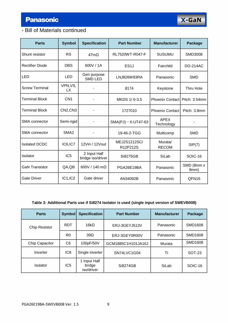
Bill of Materials Table 2: Bill of Materials
Parts Symbol Specification Part Number Manufactur
er Package
Chip
Resistor
RA1,RB1 33Ω ERJ-6ENF33R0V Panasonic SMD2012
RA2, RB2 0Ω ERJ-6GEY0R00V Panasonic SMD2012
RA3,RB3 1Ω ERJ-6GEYJ1R0V Panasonic SMD2012
RA4,RB4 - N.M. - SMD1608
RA5,RB5 82kΩ ERJ-3GEYJ823V Panasonic SMD1608
RA6,RB6 - N.M. - SMD1608
RA7,RB7 0Ω ERJ-3GEY0R00V Panasonic SMD1608
RA8,RB8 51Ω ERJ-3GEYJ510V Panasonic SMD1608
RA9,RB9 3kΩ N.M. - SMD1608
RA10, RB10 39Ω ERJ-3GEYJ390V Panasonic SMD1608
RBS - Bootstrap resistor - SMD3216
RLED 1.8 kΩ ERJ-3GEYJ182V Panasonic SMD1608
RLO/RHI 10kΩ ERJ-3GEYJ103V Panasonic SMD1608
Chip
Capacitor
C1A,C1B 1.5uF/630V ECW-FE2J155J Panasonic Axial
C2,C3 0.1uF/1000V GRJ55DR73A104KWJ1L Murata SMD5750
C4 4.7uF/10V GRM185C81A475ME11D Murata SMD1608
C5 0.1uF/50V GCJ188R71H104KA12D Murata SMD1608
CA1,CB1 2.2uF/25V GRM31MR71E225KA93L Murata SMD3216
CA2,CB2 2.2uF/25V GRM31MR71E225KA93L Murata SMD3216
CA3,CB3 330pF/100V GCM2165C2A331FA16D Murata SMD2012
CA4,CB4 0.22uF/25V GCM188R71E224KA55D Murata SMD1608
CA5,CB5 0.47uF/25V GCM188R71E474KA64D Murata SMD1608
CA6,CB6 4.7uF/16V GCG21BR71C475KA12L Murata SMD2012
CA7,CB7 1uF/50V GCG188R71C105KA01D Murata SMD1608
CA8,CB8 4.7uF/25V GCM21BC71E475KE36L Murata SMD2012
CA9,CB9 100pF/50V GCM1885C1H101JA16J Murata SMD1608
CA10,CB10 - N.M. - SMD1608
CA11,CB11 10uF/25V GRM32DR71E106KA12L Murata SMD3216
CA12,CB12 47pF/50V GCM1885C1H470JA16D Murata SMD1608
CA14,CB14 22uF/25V GRM32ER71E226KE15K Murata SMD3225
PGA26E19BA-SWEVB008 Ver. 1.5 9
- Bill of Materials continued
Parts Symbol Specification Part Number Manufacturer Package
Shunt resistor RS 47mΩ RL7520WT-R047-F SUSUMU SMD3008
Rectifier Diode DBS 600V / 1A ES1J Fairchild DO-214AC
LED LED Gen purpose
SMD LED LNJ826W83RA Panasonic SMD
Screw Terminal VPN,VS,
LX - 8174 Keystone Thru Hole
Terminal Block CN1 - MKDS 1/ 6-3,5 Phoenix Contact Pitch: 3.54mm
Terminal Block CN2,CN3 - 1727010 Phoenix Contact Pitch: 3.8mm
SMA connector Semi-rigid - SMA(PJ)-X-UT47-63 APEX
Technology -
SMA connector SMA2 - 19-46-2-TGG Multicomp SMD
Isolated DCDC IC6,IC7 12Vin / 12Vout MEJ2S1212SC/
R12P212S
Murata/
RECOM SIP(7)
Isolator IC5 2 Input Half
bridge iso/driver Si8275GB SiLab SOIC-16
GaN Transistor QA,QB 600V / 140 mΩ PGA26E19BA Panasonic SMD (8mm x
8mm)
Gate Driver IC1,IC2 Gate driver AN34092B Panasonic QFN16
Table 3: Additional Parts use if Si8274 Isolator is used (single input version of SWEVB008)
Parts Symbol Specification Part Number Manufacturer Package
Chip Resistor
RDT 16kΩ ERJ-3GEYJ513V Panasonic SMD1608
R0 39Ω ERJ-3GEY0R00V Panasonic SMD1608
Chip Capacitor C6 100pF/50V GCM1885C1H101JA16J Murata SMD1608
Inverter IC8 Single inverter SN74LVC1G04 TI SOT-23
Isolator IC5 1 Input Half
bridge iso/driver
Si8274GB SiLab SOIC-16

PGA26E19BA-SWEVB008 Ver. 1.5 10
PCB Layout PCB Specifications:
Double-sided
Size: 82mm × 122mm
Copper thickness: 70um
Board thickness: 1.6mm
Figure 4: Top and Bottom PCB Layout

PGA26E19BA-SWEVB008 Ver. 1.5 11
Test circuits
- Slew rate test circuit
Figure 5: Low Side slew rate Test circuit
When the inductor L1 is connected between VPN and LX, boost configuration is formed (also refer as low
side test). The low side GaN transistor QA is active in boost mode. The pulses generated by dead time
circuit to drive isolator SI8275GB must not be overlapping. This is to prevent both QA and QB turn on at the
same time and the shoot-through current could damage the circuit.
Figure 6: High Side slew rate Test circuit
When the inductor L1 is connected between LX and VS, buck configuration is formed (also refer as high side
test). Please note that the output connection of the dead time circuit is changed accordingly so the high side
GaN transistor QB acts as active power switch in buck mode.

PGA26E19BA-SWEVB008 Ver. 1.5 12
- Switching loss test circuit Inductor L1 is connected between VPN and LX, same as low side dV/dT test. The VDS connection is between QA Drain and Source2 pin. The VGS is not monitored to avoid shorting the Source1 and Source2 pin of the GaN device QA. The voltage across RS is measured by connecting an SMA cable to a 50 ohm terminated channel of the oscilloscope. Loss Test procedure is explained further in page 17.
- Dead time circuit
Dead time circuit is required to ensure both GaN transistor QA and QB do not turn ON at the same time.
Figure 8 shows a simple example of dead time adjustment circuit. The phasing of inverting and non-inverting
outputs can be fine-tuned by adjusting resistor R1. XOR1 and XOR4 logic gate produce compliment of the
input signal. XOR2 and XOR3 logic gate output the signals with the delay time. The delay times can be set
by adjusting the passive components R2 and R3.
Figure 8: Dead Time Circuit
Figure 7: Low Side Loss Test circuit

PGA26E19BA-SWEVB008 Ver. 1.5 13
- Efficiency test circuit Figure 9 shows SWEVB008 in DCDC synchronous boost with bootstrap high side bias circuit. The high side
Isolated DCDC was disconnected by removing the jumper JP. Bootstrap bias circuit is possible because of
the fix duty of 50%. The bootstrap resistor, RBS, is set to 0.5Ω for 100 kHz operation. For higher frequency
operation, do consider reducing the resistance or adopting an isolated DC-DC as shown in Figure 10. The
bootstrap resistor is not mounted on the board.
Figure 9 Circuit for efficiency test with high side circuit powered by bootstrap diode circuit.
Figure 10 Circuit for efficiency test with high side circuit powered by isolated DCDC.

PGA26E19BA-SWEVB008 Ver. 1.5 14
Equipment The equipment used in the evaluation test circuits is shown in Table 4. This is for reference only.
Table 4: List of Equipment used
No. Equipment Specifications Suggested Model
1 DC Power ① 1 OUTPUT
DC 600V 700W Keysight N5752A
2 DC Power ②③
2 OUTPUT
DC18V 1.5A Kenwood PW18-3
3 Pulse Generator - Agilent 33250A
4 Dead time circuit - General purpose / Basic dead time circuit 100ns
5 Power meter 3 channel power meter Yokogawa WT500
6 Electronic Load 450V/4.5kW Chroma 63804
7 Oscilloscope - Tektronix DPO7104C
8 Probe
- TCP0030 Current Probe (IL)
- P6139B Voltage Probe (VDS, VGS)
- P5205A Differential Voltage Probe (VDS)
- BNC to SMA Cable (VRS)

PGA26E19BA-SWEVB008 Ver. 1.5 15
Table 5: Double Pulse Setting with L=320uH
Figure 11: Usage of coil wire
Measurement Procedures 1) Slew Rate dV/dT tests
Initial steps: Do all the necessary connection between the evaluation board, components and equipment. Connect DC power ① to VPN and VS of the board with
the screw terminal block. Connect deadtime circuit to the IN_H, IN_L, VDD, EN and
GND terminal of the board. Please note that the connection of dead time circuit to the IN_H and IN_L depending on low side test or high side test (please refer to page 11).
Connect the inductor from VPN to LX for boost mode (low side test) or connect inductor from LX to VS for buck mode (high side test).
The VDD voltage must be 3.3V-5V, Isolator VDDI voltage range. Fix the dead time to 100ns.
Connect the dead time generator to a pulse generator. Connect DC power ② to VDD/GND terminal of the board to3.3/5V.
Connect DC power ③ to AUXH+/AUXH-, AUXL+/AUXL- terminal of
the board. Probe the point where you want to monitor and observe the
waveform using oscilloscope. Be careful not to short with other parts. It is recommended to use a coil wire fixture mounted near SMA2 on the evaluation board for VDS monitoring refer to Figure 11. Use an SMA to Tektronics probe adaptor as shown in Figure 12.
Start-up: Set up the Dead time generator circuit with the amplitude 0-5V and having the double pulse profile as
shown below:
Figure 13: Double Pulse
Again, ensure that the pulse generated occurs only in the burst mode. If the pulse is generated continuously, the transistor will be damaged by high current flows.
Set DC power ②to 5V. LED will glow to indicate EN (Si8275GB Enable pin) is high
Adjust DC power ③ to 12V gradually. Check VGS waveform when a double pulse is inputted from pulse generator. Ensure to carry out this
step with DC power ① is set to 0V.
Then, the voltage of DC power ① is gradually increased from 0V to predetermined voltage (400V).
Monitor the VDS voltage with oscilloscope and confirm that the VDS voltage rises to the set value. Input a double pulse with the pulse generator again and check the VGS, VDS and IL waveform. Observation of waveform will be easier if the trigger is applied at the rising / falling edge of VGS or VDS as shown on Figure 13 above. If different inductor value is used other than the suggested, please set the pulse width until the desired
IL value is achieved.
IL #1
2.5A 2.3µs
5A 4.6µs
7.5A 6.9µs
10A 9.2µs
Figure 12: SMA to Probe

PGA26E19BA-SWEVB008 Ver. 1.5 16
T-on
400V
0V
40V
360V
VDS at
Turn On VDS at
Turn Off
T-off
Shutdown:
Set the DC power ① slowly to 0V and then follow by the DC power ② and ③ to 0V. Turn off the power. Check the VDS waveform and ensure that the capacitor between VPN and VS terminals has fully discharged. There is risk of electric shock due to the residual charge. Measurement of dV/dt for Turn On/Off Switching Characteristics: The range used is 10%~90% IL condition is set at 2.5A / 5A / 7.5A / 10A with 16 times averaging Therefore, the dv/dt at turn on: 320V / T-on and the dv/dt at turn off: 320V / T-off
VDS dV/dT measurement during Low side device (QA) testing
Figure 14: Measurement points for Low side device
VDS dV/dT measurement during High side device (QB) testing
Figure 15: Measurement points for High side device
T-off
400V
0V
40V
360V
VDS at
Turn Off VDS at
Turn On
T-on

PGA26E19BA-SWEVB008 Ver. 1.5 17
2) Switching Loss
Initial steps: Do all the necessary connection between the evaluation board, components and equipment. Connect DC power ① to VPN and VS of the board with the screw terminal block.
Connect dead time circuit to the IN_H, IN_L, VDD, EN and GND terminal of the board. The loss test is done in boost mode (low side test). Therefore, Inductor is connected from VPN to LX.
The VDD voltage must be the same as the Isolator VDD voltage. Fix the dead time to 100ns. Connect the dead time generator to a pulse generator. Probe the point where you want to monitor and observe the waveform using oscilloscope.
Be careful not to short with other parts. Use the coil wire fixture mounted on the evaluation board for VDS and IL monitoring.
Use the semi-rigid to monitor VRS waveform. Use the Math Function on the oscilloscope to get IDS waveform. IDS = VRS /RS. RS is 47mΩ as shown in the BOM List (page 9).
Use the math function on oscilloscope to find the multiplication of VDS and IDS, then use the
measure function on the oscilloscope to find the area under the curve (power loss). See Figure 16.
Figure 16: Power Loss measurement waveform
Start-up: Set up the Dead time generator circuit with the amplitude 0-5V and having the double pulse profile as
shown in the Figure 13. Again, ensure that the pulse generated occurs only in the burst mode. If the pulse is generated
continuously, the transistor will be damaged by high current flows. Set the DC power ② to 5V gradually. Set the DC power ③ to 12V gradually. Check VGS waveform when a double pulse is inputted from pulse generator. Please carry out this step
with DC power ① is set to 0V.
Then, the voltage of DC power ① is gradually increased from 0V to predetermined voltage (400V).
Monitor the VDS voltage with oscilloscope and confirm that the VDS voltage rises to the set value. Input a double pulse with the pulse generator again and check the VGS, VDS, IDS and power loss (area
under the curve for multiplication of VDS and IDS) waveform. Observation of waveform will be easier if the trigger is applied at the rising / falling edge of VGS or VDS as
shown on Figure 16 above. If different inductor value is used other than the one provided, please set the pulse width until the
desired IL value is achieved.
Shutdown:
Set the DC power ① slowly to 0V and then follow by the DC power ② and ③ to 0V. Turn off the power. Check the VDS waveform and ensure that the capacitor between VPN and VS terminals has fully discharged. There is risk of electric shock due to the residual charge.
QA VDS
QA IDS
Power Loss (Turn On)

PGA26E19BA-SWEVB008 Ver. 1.5 18
Low Side dV/dT test Figure 17 shows all the necessary connections for Low Side GaN device (QA) dV/dT testing. Figure 18
shows the evaluation test circuit. Please refer to pages 15-16 for evaluation procedures.
Heat
Figure 17: Connection for Low Side GaN testing
Figure 18: Evaluation Schematic for Low side GaN test
AUXH+
AUXH-VPN
AUXL-
AUXL+
VDD
INH
GND
EN
GND
IN_L
VS
LX
320uH
InductorDead
Time
Circuit
N5752A DC POWER ① PW18-3
DC power ②③
5V12V
SMA to probe Adapter 33250A

PGA26E19BA-SWEVB008 Ver. 1.5 19
Switching Characteristics Result: Condition: VPN=400V, VAUXH, VAUXL=12V, RA1,RB1=33Ω, (Rout2) RA2,RB2=0/22/82Ω, RA3,RB3=1Ω, CA3,CB3=330pF
I. Low side device (QA) dV/dt Measurement Data
Figure 19: dV/dT at turn off for QA Figure 20: dV/dT at turn on for QA
II. VGS, VDS and IDS Measurement Waveform with (Rout2) RA2,RB2=0Ω
VPN=400V, IDS=2.5A VPN=400V, IDS=10A
Turn ON
dV/dt = -100.1 [V/ns] dV/dt= -75.3 [V/ns]
Turn OFF
dV/dt= 22.1 [V/ns] dV/dt= 100.3 [V/ns]
VGS 5V/div
IL 5A/div
VDS 100V/div Time scale:20ns/div
5GS/s
VGS 5V/div
IL 5A/div
VDS 100V/div
Time scale:20ns/div 5GS/s
VGS 5V/div
IL 5A/div
VDS 100V/div
Time scale:20ns/div 5GS/s VGS 5V/div
IL 5A/div
VDS 100V/div
Time scale:20ns/div 5GS/s
Important Note: The data presented is meant to demonstrate the high switching capability of Panasonic X-GaN. The dV/dT data is for reference use only and measured data maybe different depending on evaluation environment.
Figure 21: QA turn on/off waveforms at IDS=2.5A Figure 22: QA turn on/off waveforms at IDS=10A

PGA26E19BA-SWEVB008 Ver. 1.5 20
Figure 23: Connection for High side GaN test
High Side dV/dT test Figure 23 shows all the necessary connections for High Side GaN device (QB) dV/dT testing. Figure 24
shows the evaluation test circuit. Please refer to pages 15-16 for evaluation procedures.
Figure 24: Evaluation schematic for High side GaN test

PGA26E19BA-SWEVB008 Ver. 1.5 21
Switching Characteristics Result:
Condition: VPN=400V, VAUXH, VAUXL=12V, RA1,RB1=33Ω, (Rout2) RA2,RB2=0/22/82Ω, RA3,RB3=1Ω, CA3,CB3=330pF
I. High side device (QB) dV/dt Measurement Data
II. VDS and IDS Measurement Waveform with (Rout2) RA2,RB2=0Ω
VPN=400V, IDS=2.5A VPN=400V, IDS=10A
Turn ON
dV/dt = 102.6[V/ns] dV/dt = 82.3[V/ns]
Turn OFF
dV/dt = -20.8[V/ns] dV/dt = -102.9[V/ns]
IL 5A/div
VDS 100V/div
Time scale:20ns/div 5GS/s
IL 5A/div
VDS 100V/div
Time scale:20ns/div 5GS/s
IL 5A/div
VDS 100V/div Time scale:20ns/div
5GS/s
IL 5A/div
VDS 100V/div Time scale:20ns/div 5GS/s
Important Note: The data presented is meant to demonstrate the high switching capability of Panasonic X-GaN. The dV/dT data is for reference use only and measured data maybe different depending on evaluation environment.
Figure 25: dV/dT at turn off for QB Figure 26: dV/dT at turn on for QB
Figure 27: QB turn on/off waveforms at IDS=2.5A Figure 28: QB turn on/off waveforms at IDS=10A

PGA26E19BA-SWEVB008 Ver. 1.5 22
Low Side Switching Loss test Figure 29 shows all the necessary connections for Low Side GaN device (QA) Switching Loss testing. Figure
30 shows the evaluation test circuit. Please refer to page 17 for details and evaluation procedures.
Figure 29: Connection for Low side switching loss test
Figure 30: Test Circuit for Low side GaN switching lost test
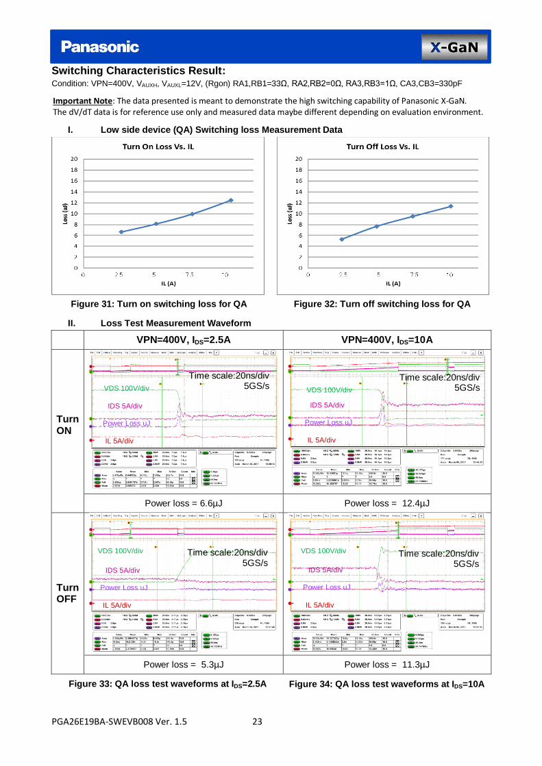
PGA26E19BA-SWEVB008 Ver. 1.5 23
Switching Characteristics Result: Condition: VPN=400V, VAUXH, VAUXL=12V, (Rgon) RA1,RB1=33Ω, RA2,RB2=0Ω, RA3,RB3=1Ω, CA3,CB3=330pF
I. Low side device (QA) Switching loss Measurement Data
II. Loss Test Measurement Waveform
VPN=400V, IDS=2.5A VPN=400V, IDS=10A
Turn ON
Power loss = 6.6µJ Power loss = 12.4µJ
Turn OFF
Power loss = 5.3µJ Power loss = 11.3µJ
Power Loss uJ
IL 5A/div
VDS 100V/div Time scale:20ns/div
5GS/s
IDS 5A/div
Time scale:20ns/div 5GS/s
Time scale:20ns/div 5GS/s
Time scale:20ns/div 5GS/s
Power Loss uJ
IL 5A/div
VDS 100V/div
IDS 5A/div
Power Loss uJ
IL 5A/div
VDS 100V/div
IDS 5A/div
VDS 100V/div
IDS 5A/div
Power Loss uJ
IL 5A/div
VDS 100V/div
IDS 5A/div
Power Loss uJ
IL 5A/div
VDS 100V/div
IDS 5A/div
Power Loss uJ
IL 5A/div
VDS 100V/div
IDS 5A/div
Power Loss uJ
IL 5A/div
VDS 100V/div
IDS 5A/div
Important Note: The data presented is meant to demonstrate the high switching capability of Panasonic X-GaN. The dV/dT data is for reference use only and measured data maybe different depending on evaluation environment.
VDS 100V/div
Figure 31: Turn on switching loss for QA Figure 32: Turn off switching loss for QA
Figure 33: QA loss test waveforms at IDS=2.5A Figure 34: QA loss test waveforms at IDS=10A

PGA26E19BA-SWEVB008 Ver. 1.5 24
Efficiency test To test the efficiency of Panasonic GaN-Tr in hard switching operation, SWEVB008 board is connected in
synchronous boost configuration. The input frequency for this test is 100kHz.
Test Conditions:
VAUXH/VAUXL=12V, RA1,RB1=33Ω, RA2,RB2=0Ω, RA3,RB3=1Ω, CA3,CB3=330pF
VIN=200V, Frequency=100kHz, Inductor=200uH, Duty=50%, Dead time=100ns
Cooling Method: Natural convection, Ta=25°C
Figure 35: Evaluation schematic for Boost DCDC Efficiency Evaluation
Figure 36: Boost DCDC Efficiency data at 100kHz

PGA26E19BA-SWEVB008 Ver. 1.5 25
Thermal Profile The thermal profile is captured during DCDC Synchronous boost test with the following test conditions:
VAUXH/VAUXL=12V, RA1,RB1 =33Ω, RA2,RB2=0Ω, RA3,RB3=1Ω, CA3,CB3=330pF
VIN=200V, VOUT=394V@450W
Frequency=100kHz, Inductor=200uH, Duty=50%, Dead Time=100ns
Cooling Method: Natural convection, Ta = 25°C
Figure 37: Thermal Profile of SWEVB008 in DCDC boost at 450W output power

PGA26E19BA-SWEVB008 Ver. 1.5 26
Thermal Cooling
Adhesive Thermal Tape: T GLOBAL Li-98 Thermal conductivity: 0.95 W/mK Conductive material: Acrylic, Fibreglass Thermal impedance: 1.8°C/W Breakdown voltage : > 3,000 Vac Operating temperature: -30 ~ 120°C
Heat Sink: Fischer Elektronik ICK SMD E15
Figure 38: Mounted Heatsink information and picture
PGA26E19BA-SWEVB008 Ver. 1.5 27
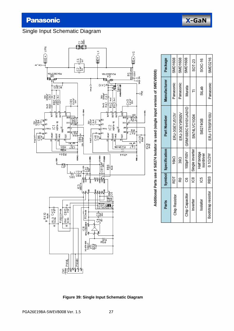
Single Input Schematic Diagram
Heat
Figure 39: Single Input Schematic Diagram

PGA26E19BA-SWEVB008 Ver. 1.5 28
Single Input Low Side dV/dT test Figure 40 shows all the necessary connections for Low Side GaN device (QA) dV/dT testing. Figure 41
shows the evaluation test circuit. Please refer to pages 15-16 for evaluation procedures.
Heat
AUXL- AUXL+
VDD NC GND EN NC NC
5V 12V
N5752A DC POWER ① PW18-3 DC power ②③
33250A
Figure 40: Connection for Low Side GaN testing
PGA26E19BA-SWEVB008 Ver. 1.5 29
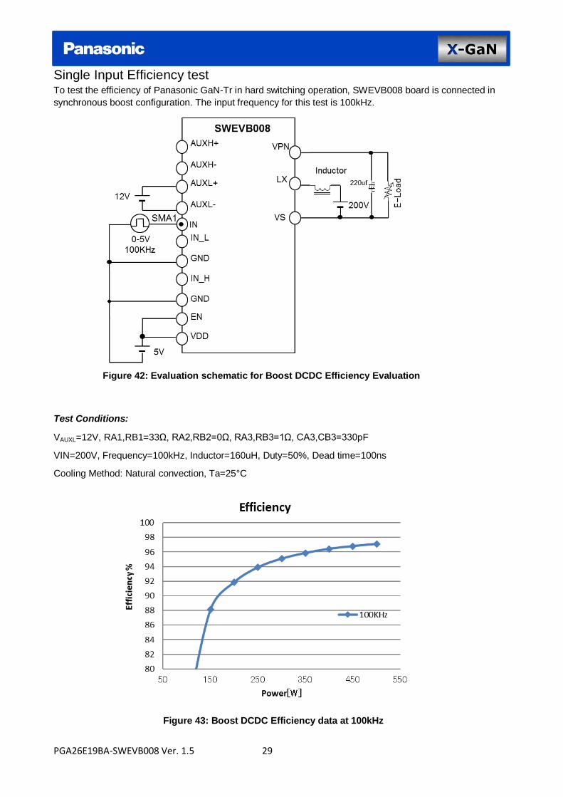
Single Input Efficiency test To test the efficiency of Panasonic GaN-Tr in hard switching operation, SWEVB008 board is connected in
synchronous boost configuration. The input frequency for this test is 100kHz.
Test Conditions:
VAUXL=12V, RA1,RB1=33Ω, RA2,RB2=0Ω, RA3,RB3=1Ω, CA3,CB3=330pF
VIN=200V, Frequency=100kHz, Inductor=160uH, Duty=50%, Dead time=100ns
Cooling Method: Natural convection, Ta=25°C
Figure 42: Evaluation schematic for Boost DCDC Efficiency Evaluation
Figure 43: Boost DCDC Efficiency data at 100kHz

PGA26E19BA-SWEVB008 Ver. 1.5 30
Important Notice Please read and understand the following items, "Restriction", and "Caution" before using the evaluation board:
Restriction
The evaluation board is intended for use as engineering development, verification or evaluation purposes only.
This evaluation board is not intended for a finished end-product fit for general consumer use.
Do not operate in condition other than the recommended settings.
The evaluation board must be used only by qualified engineers and technicians that have electronics training, familiar with handling of high-voltage electrical systems and observe good engineering practise standards.
The evaluation board is meant to be operated in lab environment under the safe conditions.
Please use a protective case (accessory) during evaluation.
All of the specifications and evaluation data in this manual are for reference only and not guaranteed. The information may subject to change without notice. Please contact to Panasonic representative for the latest information.
The user assumes all responsibility and liability for proper and safe handling of this evaluation board. Further, the user indemnifies Panasonic from all claims arising from the handling or use of the evaluation boards.
The technical information described in this document is intended only to show the main characteristics and application circuit examples of the products. No license is granted in and to any intellectual property right or other right owned by Panasonic Corporation or any other company. Therefore, no responsibility is assumed by our company as to the infringement upon any such right owned by any other company which may arise as a result of the use of technical information described in this document.
Caution
The evaluation board carries hazardous high voltage. Do not touch when power is applied. Otherwise, it may cause severe injury, disability or death.
Electric charge may be accumulated in the capacitors. To prevent electrical shock, please ensure all the capacitors are properly discharged before touching the evaluation board.
It is the user’s responsibility to confirm that the voltages, isolation requirements, and rated value are identified and understood, prior to handling the evaluation board.
Do not leave the evaluation board unattended while power is applied and do not perform other activity near the evaluation board while power is applied.
This board contains parts that are susceptible to damage by electrostatic discharge (ESD). It is the user’s responsibility to take any and all appropriate precautions with regard to electrostatic discharge when using the evaluation board.
Should the evaluation board does not meet the specification indicated in the application note, the board may be exchanged with a new one within 30 days from the date of delivery. When exchanging the evaluation board, please return the board with all items included.
The warranty on this evaluation board is considered void once a part on the board is removed or modified.
The evaluation board does not fall within the scope of the technical requirements of the following directives or other related directives:
- Restriction of Hazardous Substances (RoHS) - Directive on Waste Electrical and Electronic Equipment (WEEE) - Mandatory conformity marking for products sold in the European Economic Area (CE) - Federal Communications Commission (FCC) - Underwriters Laboratories, Inc. (UL)

PGA26E19BA-SWEVB008 Ver. 1.5 31

Request for your special attention and precautionsin using the technical information and semiconductors described in this book
(1) If any of the products or technical information described in this book is to be exported or provided to non-residents, thelaws and regulations of the exporting country, especially, those with regard to security export control, must be observed.
(2) The technical information described in this book is intended only to show the main characteristics and application circuitexamples of the products. No license is granted in and to any intellectual property right or other right owned byPanasonic Corporation or any other company. Therefore, no responsibility is assumed by our company as to theinfringement upon any such right owned by any other company which may arise as a result of the use of technicalinformation de-scribed in this book.
(3) The products described in this book are intended to be used for general applications (such as office equipment,communications equipment, measuring instruments and household appliances), or for specific applications as expresslystated in this book.Please consult with our sales staff in advance for information on the following applications, moreover please exchangedocuments separately on terms of use etc.: Special applications (such as for in-vehicle equipment, airplanes, aerospace,automotive equipment, traffic signaling equipment, combustion equipment, medical equipment and safety devices) inwhich exceptional quality and reliability are required, or if the failure or malfunction of the products may directlyjeopardize life or harm the human body.Unless exchanging documents on terms of use etc. in advance, it is to be understood that our company shall not be heldresponsible for any damage incurred as a result of or in connection with your using the products described in this bookfor any special application.
(4) The products and product specifications described in this book are subject to change without notice for modificationand/or improvement. At the final stage of your design, purchasing, or use of the products, therefore, ask for the most up-to-date Product Standards in advance to make sure that the latest specifications satisfy your requirements.
(5) When designing your equipment, comply with the range of absolute maximum rating and the guaranteed operatingconditions (operating power supply voltage and operating environment etc.). Especially, please be careful not to exceedthe range of absolute maximum rating on the transient state, such as power-on, power-off and mode-switching. Other-wise, we will not be liable for any defect which may arise later in your equipment.Even when the products are used within the guaranteed values, take into the consideration of incidence of break downand failure mode, possible to occur to semiconductor products. Measures on the systems such as redundant design,arresting the spread of fire or preventing glitch are recommended in order to prevent physical injury, fire, social damages,for example, by using the products.
(6) Comply with the instructions for use in order to prevent breakdown and characteristics change due to external factors(ESD, EOS, thermal stress and mechanical stress) at the time of handling, mounting or at customer's process. We donot guarantee quality for disassembled products or the product re-mounted after removing from the mounting board.When using products for which damp-proof packing is required, satisfy the conditions, such as shelf life and the elapsedtime since first opening the packages.
(7) When reselling products described in this book to other companies without our permission and receiving any claim ofrequest from the resale destination, please understand that customers will bear the burden.
(8) This book may be not reprinted or reproduced whether wholly or partially, without the prior written permission of ourcompany.
No.010618