PFC THD Reduction and Efficiency Improvement by … – April 2012 2 PFC THD Reduction and...
15
Application Report SLUA644 – April 2012 1 PFC THD Reduction and Efficiency Improvement by ZVS or Valley Switching Bosheng Sun, Zhong Ye High Performance Isolated Abstract When a PFC is in discontinuous conduction mode, the inductor current will resonant between the boost inductor and MOSFET parasite capacitance. The resonant current can be big enough to distort the PFC current significantly. This application note introduces a digital control scheme based on UCD3XXX to predict the position at which the resonant current first time rises back from negative to zero, and turning on the MOSFET at this position to minimize PFC current distortion. Since the switch node is either zero voltage or valley voltage at this position, the efficiency is also improved. Contents Introduction .......................................................................................................................................... 2 ZVS or valley switching control .......................................................................................................... 3 Firmware implementation.................................................................................................................... 6 ZVS and Valley Switching Experiment and Test Results .................................................................. 7 Conclusion ......................................................................................................................................... 14 Figures Figure 1. Experimental digitally controlled 360W PFC circuit ...................................................... 2 Figure 2. A typical current distortion waveform at light loads ..................................................... 3 Figure 3. Resonation between boost inductor and MOSFET output capacitance when Vin < 1/2Vout .................................................................................................................... 3 Figure 4. Resonation between boost inductor and MOSFET output capacitance when Vin > 1/2Vout .................................................................................................................... 4 Figure 5. Effect of nonlinear parasitic capacitance ...................................................................... 5 Figure 6. PFC current harmonic reduction and ZVS/ZCS operation at low line and 10% load ................................................................................................................................... 9 Figure 7. PFC current harmonic reduction and ZVS/ZCS operation at high line and 20% load ................................................................................................................. 11 Figure 8. THD, FP and efficiency comparison with and without ZVS or valley switching at low line ....................................................................................................................... 12 Figure 9. THD, FP and efficiency comparison with and without ZVS or valley switching at high line.......................................................................................................................... 13
Transcript of PFC THD Reduction and Efficiency Improvement by … – April 2012 2 PFC THD Reduction and...
Application Report SLUA644 – April 2012
1
PFC THD Reduction and Efficiency Improvement by ZVS or Valley Switching
Bosheng Sun, Zhong Ye High Performance Isolated
Abstract When a PFC is in discontinuous conduction mode, the inductor current will resonant between the boost inductor and MOSFET parasite capacitance. The resonant current can be big enough to distort the PFC current significantly. This application note introduces a digital control scheme based on UCD3XXX to predict the position at which the resonant current first time rises back from negative to zero, and turning on the MOSFET at this position to minimize PFC current distortion. Since the switch node is either zero voltage or valley voltage at this position, the efficiency is also improved.
Contents Introduction .......................................................................................................................................... 2 ZVS or valley switching control .......................................................................................................... 3 Firmware implementation .................................................................................................................... 6 ZVS and Valley Switching Experiment and Test Results .................................................................. 7 Conclusion ......................................................................................................................................... 14
Figures Figure 1. Experimental digitally controlled 360W PFC circuit ...................................................... 2 Figure 2. A typical current distortion waveform at light loads ..................................................... 3 Figure 3. Resonation between boost inductor and MOSFET output capacitance when
Vin < 1/2Vout .................................................................................................................... 3 Figure 4. Resonation between boost inductor and MOSFET output capacitance when
Vin > 1/2Vout .................................................................................................................... 4 Figure 5. Effect of nonlinear parasitic capacitance ...................................................................... 5 Figure 6. PFC current harmonic reduction and ZVS/ZCS operation at low line and 10%
load ................................................................................................................................... 9 Figure 7. PFC current harmonic reduction and ZVS/ZCS operation at high line
and 20% load ................................................................................................................. 11 Figure 8. THD, FP and efficiency comparison with and without ZVS or valley switching
at low line ....................................................................................................................... 12 Figure 9. THD, FP and efficiency comparison with and without ZVS or valley switching at
high line.......................................................................................................................... 13

SLUA644 – April 2012
2 PFC THD Reduction and Efficiency Improvement by ZVS or Valley Switching
Introduction A PFC circuit, as shown in Figure1, with power level over 200W usually uses average-current mode control and operates at a constant switching frequency. The circuit’s boost inductor current iL can maintain continuous-conduction mode (CCM) for certain heavy load range. However, at light loads, the current becomes discontinuous. Once the boost inductor current declines to zero, the boost inductor, L, resonates with PFC MOSFET Q1’s parasite capacitance C1.
D1
Q1Q2
+Co
C1
L
iacVc
Syn
VL,VN ADCIref
Gv1/Vrms +Vref
Kf
Vo
Iref
Vrms Gv1/ 2
VrefKmABC
B
C
A
EADC + CLA + DPWM
Fusion Digital Power Controller
Is
C2
D2 R
iL
Figure1. Experimental digitally controlled 360W PFC circuit.
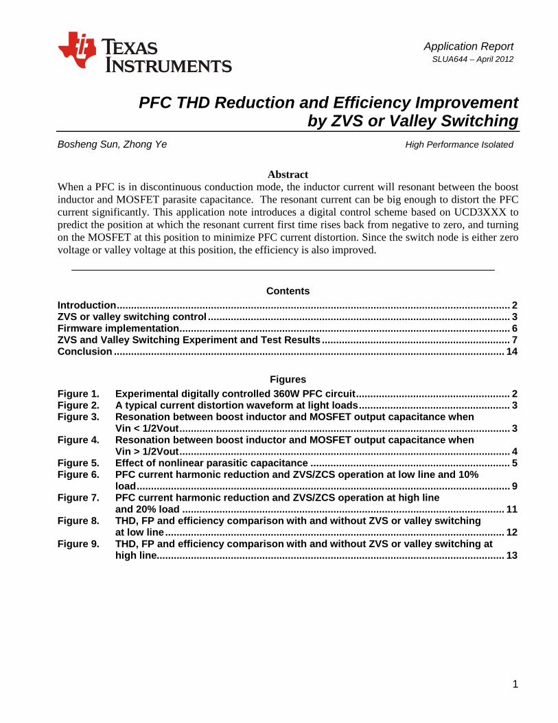
The resonant current can be big enough to distort the PFC current significantly, as shown in Figure 2a. Depending on the MOSFET’s turn-on time, the resonant current contributes to average current in a different way in one switching cycle. In another word, the resonant current adds to the switching current in one switching cycle, but in next switching cycle, the current is subtracted from the switching current, which causes large current steps, as shown in zoom-in waveforms of Figure 2b. Since this effect occurs at much higher frequency than a PFC’s current loop bandwidth at discontinuous-conduction mode (DCM), the current loop can not regulate the boost inductor current fast enough to compensate the abrupt current disturbance.
(a)
Vac
iL
iac
SLUA644 – April 2012
PFC THD Reduction and Efficiency Improvement by ZVS or Valley Switching 3
(b)
Figure2. A typical current distortion waveform at light loads.
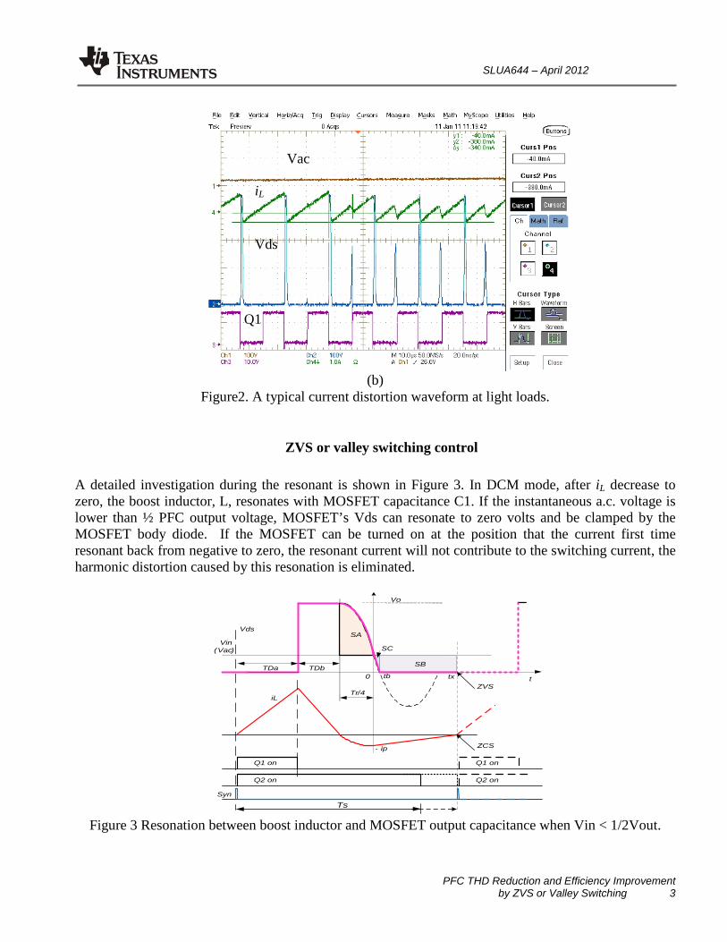
ZVS or valley switching control A detailed investigation during the resonant is shown in Figure 3. In DCM mode, after iL decrease to zero, the boost inductor, L, resonates with MOSFET capacitance C1. If the instantaneous a.c. voltage is lower than ½ PFC output voltage, MOSFET’s Vds can resonate to zero volts and be clamped by the MOSFET body diode. If the MOSFET can be turned on at the position that the current first time resonant back from negative to zero, the resonant current will not contribute to the switching current, the harmonic distortion caused by this resonation is eliminated.
VdsSA
SB
SC
0 tb tx
Vo
Vin (Vac)
Tr/4
TDbTDa
- ip
Q1 on
iL
Q1 on
Ts
ZVS
ZCS
t
Q2 on Q2 on
Syn
Figure 3 Resonation between boost inductor and MOSFET output capacitance when Vin < 1/2Vout.
Vds
iL
Vac
Q1
SLUA644 – April 2012
4 PFC THD Reduction and Efficiency Improvement by ZVS or Valley Switching
For PFC controlled by digital controller such as UCD3XXX, this position can be pre-calculated as follow: For steady state operation, a boost inductor’s Volt·Second (V·S) is balance in each switching cycle. Given Q1 turn-on time TDa, the time for the boost inductor current iL to return to zero is,
TDb = TDa* Vin /(Vo-Vin) (1) During this resonation period when the boost inductor current iL resonates back from negative value to zero at time tx, the V·S applied to the boost inductor maintains balanced as well. By using V·S balancing again, SA = SB + SC, Tx can be calculated as follow:
2)(1**
)(*1VpVin
rVinVp
VpVinarcSin
rtx −+=
ωω (2)
where Vp = (Vo-Vin) and ωr is the angular frequency of the resonant circuit (ωr = 1/2π Tr) . Equation (2) can be simplified to reduce processor computing time and an approximate tx value can be calculated by,
tx = Vo · Tr / (8 · Vin) (3) From equations (1) and (2) or (3),
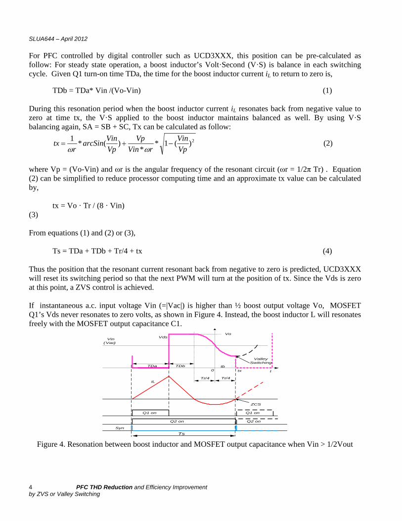
Ts = TDa + TDb + Tr/4 + tx (4) Thus the position that the resonant current resonant back from negative to zero is predicted, UCD3XXX will reset its switching period so that the next PWM will turn at the position of tx. Since the Vds is zero at this point, a ZVS control is achieved. If instantaneous a.c. input voltage Vin (=|Vac|) is higher than ½ boost output voltage Vo, MOSFET Q1’s Vds never resonates to zero volts, as shown in Figure 4. Instead, the boost inductor L will resonates freely with the MOSFET output capacitance C1.
Vds
0tb
tx
VoVin
(Vac)
Tr/4
TDbTDa
Tr/4
Q1 on Q1 on
Ts
Valley Switching
ZCS
iL
t
Q2 on Q2 on
Syn
Figure 4. Resonation between boost inductor and MOSFET output capacitance when Vin > 1/2Vout

SLUA644 – April 2012
PFC THD Reduction and Efficiency Improvement by ZVS or Valley Switching 5
In this case, tx is equals to Tr/4 and the predict switching period become,
Ts = TDa + TDb + Tr/4 + Tr/4 (5) If the next PWM turns on at the position of tx, there is no ZVS as Vds is not zero, however, Vds is at its lowest point, this is called valley switching. A simple hardware as shown in Figure 1 is used to implement this new control algorithm. Q1 is controlled by PFC’s average mode current loop. Q2 is turned on at the same time of Q1 but turned off at the end of the predicted switching period Ts. A Synchronize signal is generated at the position tx to restart the next PWM pulse. The PFC is running with either ZVS or valley switching. The above analysis assuming the MOSFET’s output capacitance is constant. However, the MOSFET’s output capacitance is actually non-linear vs. its drain to source voltage. The output capacitance of a typical MOSFET, such as SPP20N60C3, maintains relatively constant from 600V down to 50V, but the value increases by about 10 times at Vds=25V and nearly 100 times at Vds=0V. The nonlinearity introduces some error to the calculation when the instantaneous a.c. voltage is lower than ½ PFC output voltage. The waveforms are shown in Figure 5. When Vds valley voltage is lower than 50V, the nonlinear characteristic of the MOSFET output capacitance starts to affect Vds waveform, as shown in dash line in Figure 5. The actual valley occurs later than the calculated position. However, since the valley becomes flat, the switching loss increase caused by the premature turning-on of the MOSFET is insignificant.
Vds
0tb
tx
VoVin
(Vac)
Tr/4
TDbTDa
Tr/4
/4Tr’
Flat Valley
Figure 5. Effect of nonlinear parasitic capacitance.
To ensure ZVS, instead of solely using Ts to update PWM switching period, a diode D2 connects to the switch node is proposed to provide a more reliable control. Q2 could be turned off too early due to calculation error, however, since Vds is still zero at this point, the Syn signal is blocked by D2 until the real tx is coming. When load is increased and the boost inductor current is continuous, the calculated period Ts (=TDa + TDb + Tr/4 + tx) becomes always larger than the PWM switching period (= TDa + TDb). A new switching period starts before Q2 is turned off, therefore Q2 is on all the time and Syn remains low. For this case, the PFC returns to conventional hard-switching CCM operation disregarding input a.c. voltage.
SLUA644 – April 2012
6 PFC THD Reduction and Efficiency Improvement by ZVS or Valley Switching
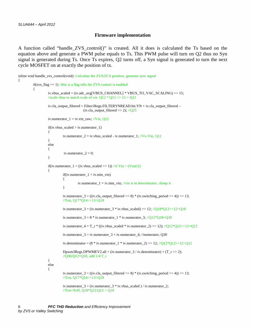
Firmware implementation A function called “handle_ZVS_control()” is created. All it does is calculated the Ts based on the equation above and generate a PWM pulse equals to Ts. This PWM pulse will turn on Q2 thus no Syn signal is generated during Ts. Once Ts expires, Q2 turns off, a Syn signal is generated to turn the next cycle MOSFET on at exactly the position of tx. inline void handle_zvs_control(void) //calculate the ZVS/ZCS position, generate sync signal {
if(zvs_flag == 1) //this is a flag tells the ZVS control is enabled { iv.vbus_scaled = (iv.adc_avg[VBUS_CHANNEL] * VBUS_TO_VAC_SCALING) >> 15; //scale vbus to match scale of vin Q12 * Q15 >> 15 = Q12
iv.cla_output_filtered = Filter1Regs.FILTERYNREAD.bit.YN + iv.cla_output_filtered – (iv.cla_output_filtered >> 2); //Q25 iv.numerator_1 = iv.vin_raw; //Vin, Q12 if(iv.vbus_scaled > iv.numerator_1) {
iv.numerator_2 = iv.vbus_scaled - iv.numerator_1; //Vo-Vin, Q12 } else
{ iv.numerator_2 = 0;
}
if(iv.numerator_1 < (iv.vbus_scaled >> 1)) //if Vin < (Vout/2) {
if(iv.numerator_1 < iv.min_vin) { iv.numerator_1 = iv.min_vin; //vin is in denominator, clamp it } iv.numerator_3 = ((iv.cla_output_filtered >> 8) * (iv.switching_period >> 4)) >> 13; //Ton, Q17*Q14>>13=Q18 iv.numerator_3 = (iv.numerator_3 * iv.vbus_scaled) >> 12; //Q18*Q12>>12=Q18 iv.numerator_3 = 8 * iv.numerator_1 * iv.numerator_3; //Q12*Q18=Q30 iv.numerator_4 = T_r * ((iv.vbus_scaled * iv.numerator_2) >> 12); //Q12*Q12>>12=Q12 iv.numerator_3 = iv.numerator_3 + iv.numerator_4; //numerator, Q30 iv.denominator = (8 * iv.numerator_1 * iv.numerator_2) >> 12; //Q12*Q12>>12=Q12 Dpwm3Regs.DPWMEV2.all = (iv.numerator_3 / iv.denominator) + (T_r >> 2); //Q30/Q12=Q18, add 1/4 T_r
} else {
iv.numerator_3 = ((iv.cla_output_filtered >> 8) * (iv.switching_period >> 4)) >> 13; //Ton, Q17*Q14>>13=Q18 iv.numerator_3 = (iv.numerator_3 * iv.vbus_scaled ) / iv.numerator_2; //Ton+Toff, Q18*Q12/Q12 = Q18

SLUA644 – April 2012
PFC THD Reduction and Efficiency Improvement by ZVS or Valley Switching 7
Dpwm3Regs.DPWMEV2.all = iv.numerator_3 + (T_r >> 1); //Ton+Toff+1/2 T_r
} Dpwm1Regs.DPWMSAMPTRIG1.all=Dpwm3Regs.DPWMEV2.all-(iv.sample_trigger_offset<<2); //PWM frequency changed, update sample trigger accordingly
} else { Dpwm1Regs.DPWMSAMPTRIG1.all = iv.switching_period - (iv.sample_trigger_offset * 4); // sample at the end of period }
} At heavy load, the PFC enters CCM mode, there is no need to apply this control scheme any more. At high line, although this control scheme can achieve valley switching, the PWM frequency is also increased, the efficiency may or may not improved. The following function will automatically disable the control scheme at heavy load or high line. inline void dynamic_system_optimization(void) {
if(iv.vin_squared_average < 0x1400) //if vin < 160 volts {
if(iv.pis.output < 0x600) //enable ZVS control at light load {
zvs_flag = 1; //enable ZVS control at light load Dpwm1Regs.DPWMCTRL1.bit.EXT_SYNC_EN = 1; //sync to external Dpwm3Regs.DPWMCTRL0.bit.MSYNC_SLAVE_EN = 0; Dpwm3Regs.DPWMCTRL1.bit.EXT_SYNC_EN = 1; //sync to external
} else if(iv.pis.output > 0x650) //disable ZVS at heavy load {
zvs_flag = 0; //disable zvs control Dpwm1Regs.DPWMCTRL1.bit.EXT_SYNC_EN = 0; Dpwm3Regs.DPWMCTRL0.bit.MSYNC_SLAVE_EN = 1; Dpwm3Regs.DPWMCTRL1.bit.EXT_SYNC_EN = 0;
} } else //high line {
if(zvs_flag == 1) //disable ZVS at high line {
zvs_flag = 0; //disable zvs control Dpwm1Regs.DPWMCTRL1.bit.EXT_SYNC_EN = 0; Dpwm3Regs.DPWMCTRL0.bit.MSYNC_SLAVE_EN = 1; Dpwm3Regs.DPWMCTRL1.bit.EXT_SYNC_EN = 0;
} }
}
ZVS and Valley Switching Experiment and Test Results This predictive ZVS or valley switching control scheme is implemented in TI’s PFC EVM PWR026 and PR977. The following results are gathered from PR977. Figure 5a shows input current waveforms at 120Vac input and 10% load with conventional fix frequency hard switching control. Figure 5b shows the

SLUA644 – April 2012
8 PFC THD Reduction and Efficiency Improvement by ZVS or Valley Switching
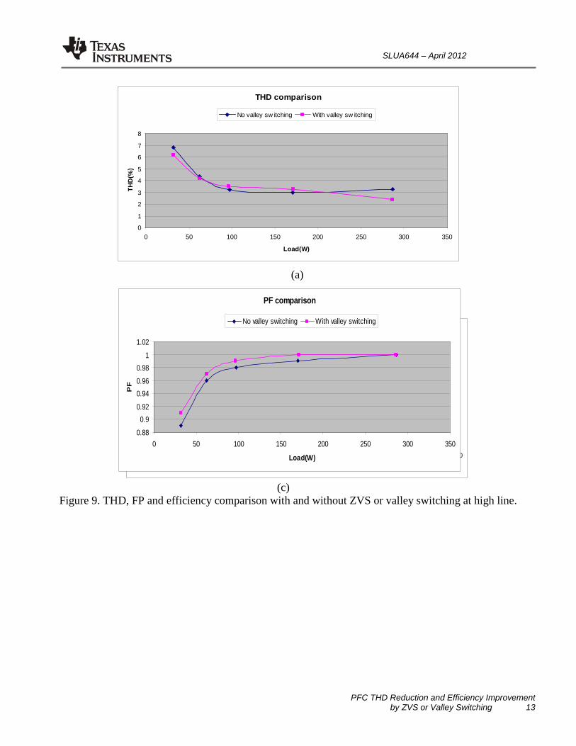
reduction of current harmonic after using this method. It can be seen that low frequency current distortion at the crossover points was almost completely eliminated. THD was reduced from 5.25% to 4.18% while efficiency was improved over 2%. Figure5c shows the PFC MOSFET achieves both ZVS and ZCS. At high line input and light loads, MOSFET Q1 can operate in either valley switching or ZVS/ZCS depending on the instantaneous a.c. voltage. Figure 6a and Figure 6b show current waveforms at 230V input and 20% load before and after this control is applied. The reduction of measured THD is not as significant as it appears. That is due to the 30th harmonic measurement limitation of the test equipment used. Figure 6c shows Vdc valley switching of Q1. Since the tx calculation equations are valid for both instantaneous a.c. voltages higher and lower than 1/2 Vo, no operating mode switching control is required. When the PFC operates at CCM, the computed period becomes larger than maximum PWM period, which is set based on hard-switching operation and no Syn pulse is generated. The circuit transitions between constant frequency mode and variable frequency one seamlessly. The PFC THD, Power Factor and efficiency data were collected and depicted in Figure 7 and Figure 8. Overall PFC efficiency was improved, except at high line and 10% load. The efficiency decrease at high line and 10% load was due to the additional switching loss caused by increased switching frequency. At these points, the increased switching loss surpasses the energy saved from valley switching. The digital controller knows its own switching frequency and it can calculate or measure output load to disable the valley switching control based on preset condition to avoid performance degrade and enable the control again to gain the efficient and THD benefit for the rest of operation conditions.
(a)
iac
Vac

SLUA644 – April 2012
PFC THD Reduction and Efficiency Improvement by ZVS or Valley Switching 9
(b)
(c)
Figure 6. PFC current harmonic reduction and ZVS/ZCS operation at low line and 10% load . (a) With conventional control: THD= 5.25%, PF = 0.99
(b) With ZVS control: THD= 4.18%, PF=0.99 (c) waveforms with ZVS control
Vac
iac
Vds
Q1
iL

SLUA644 – April 2012
10 PFC THD Reduction and Efficiency Improvement by ZVS or Valley Switching
(a)
(b)
Vac
Vac
iac
iac

SLUA644 – April 2012
PFC THD Reduction and Efficiency Improvement by ZVS or Valley Switching 11
(c)
Figure 7. PFC current harmonic reduction and ZVS/ZCS operation at high line and 20% load. (a) With conventional control: THD= 4.34%, PF = 0.96
(b) With valley switching control: THD= 4.18%, PF=0.97 (c) waveforms with valley switching control
iL
Vds
Q1

SLUA644 – April 2012
12 PFC THD Reduction and Efficiency Improvement by ZVS or Valley Switching
(a)
(b)
(c) Figure 8. THD, FP and efficiency comparison with and without ZVS or valley switching at low line
THD comparison
0
1
2
3
4
5
6
7
0 50 100 150 200 250 300 350
Load(W)
THD(
%)
No valley sw itching With valley sw itching
PF comparison
0.975
0.98
0.985
0.99
0.995
1
1.005
0 50 100 150 200 250 300 350
Load(W)
PF
No valley switching With valley switching
Efficiency comparison
82.0%84.0%
86.0%88.0%
90.0%92.0%
94.0%96.0%
0 50 100 150 200 250 300 350
Load(W)
Effic
ienc
y
No valley switching With valley switching
SLUA644 – April 2012
PFC THD Reduction and Efficiency Improvement by ZVS or Valley Switching 13
(a)
(b)
Efficiency comparison
0.750
0.800
0.850
0.900
0.950
1.000
0 50 100 150 200 250 300 350
Load(W)
effic
ienc
y
No valley switching With valley switching
(c) Figure 9. THD, FP and efficiency comparison with and without ZVS or valley switching at high line.
THD comparison
0
1
2
3
4
5
6
7
8
0 50 100 150 200 250 300 350
Load(W)
THD
(%)
No valley sw itching With valley sw itching
PF comparison
0.88
0.90.92
0.940.96
0.981
1.02
0 50 100 150 200 250 300 350
Load(W)
PF
No valley switching With valley switching

SLUA644 – April 2012
14 PFC THD Reduction and Efficiency Improvement by ZVS or Valley Switching
Conclusion This predictive ZVS or valley switching control scheme can be implemented by TI’s digital controller UCD3XXX. The position that the inductor current first time resonant from negative back to zero is calculated, and a simple hardware is used to generate a Syn signal at this point to restart the next PWM cycle. Since the switch node voltage is either zero or at its valley, a ZVS or valley switching is achieved. This control was proved to be valid for all line and load conditions and both CCM and DCM operations. It allows the PFC to transfer between constant frequency hard-switching mode and variable frequency ZVS or valley switching mode seamlessly without using any conditional mode switching mechanism. The control reduces current ripple significantly. It improves PFC overall performance, including THD, power factor and efficiency, at low line and light loads. Good PF improvement and some THD reduction were also achieved at high line. However, efficiency decrease was observed at below 10% load and at high line. This function can be enabled/disabled automatically by the controller based on input voltage and load condition.

IMPORTANT NOTICETexas Instruments Incorporated and its subsidiaries (TI) reserve the right to make corrections, enhancements, improvements and otherchanges to its semiconductor products and services per JESD46, latest issue, and to discontinue any product or service per JESD48, latestissue. Buyers should obtain the latest relevant information before placing orders and should verify that such information is current andcomplete. All semiconductor products (also referred to herein as “components”) are sold subject to TI’s terms and conditions of salesupplied at the time of order acknowledgment.TI warrants performance of its components to the specifications applicable at the time of sale, in accordance with the warranty in TI’s termsand conditions of sale of semiconductor products. Testing and other quality control techniques are used to the extent TI deems necessaryto support this warranty. Except where mandated by applicable law, testing of all parameters of each component is not necessarilyperformed.TI assumes no liability for applications assistance or the design of Buyers’ products. Buyers are responsible for their products andapplications using TI components. To minimize the risks associated with Buyers’ products and applications, Buyers should provideadequate design and operating safeguards.TI does not warrant or represent that any license, either express or implied, is granted under any patent right, copyright, mask work right, orother intellectual property right relating to any combination, machine, or process in which TI components or services are used. Informationpublished by TI regarding third-party products or services does not constitute a license to use such products or services or a warranty orendorsement thereof. Use of such information may require a license from a third party under the patents or other intellectual property of thethird party, or a license from TI under the patents or other intellectual property of TI.Reproduction of significant portions of TI information in TI data books or data sheets is permissible only if reproduction is without alterationand is accompanied by all associated warranties, conditions, limitations, and notices. TI is not responsible or liable for such altereddocumentation. Information of third parties may be subject to additional restrictions.Resale of TI components or services with statements different from or beyond the parameters stated by TI for that component or servicevoids all express and any implied warranties for the associated TI component or service and is an unfair and deceptive business practice.TI is not responsible or liable for any such statements.Buyer acknowledges and agrees that it is solely responsible for compliance with all legal, regulatory and safety-related requirementsconcerning its products, and any use of TI components in its applications, notwithstanding any applications-related information or supportthat may be provided by TI. Buyer represents and agrees that it has all the necessary expertise to create and implement safeguards whichanticipate dangerous consequences of failures, monitor failures and their consequences, lessen the likelihood of failures that might causeharm and take appropriate remedial actions. Buyer will fully indemnify TI and its representatives against any damages arising out of the useof any TI components in safety-critical applications.In some cases, TI components may be promoted specifically to facilitate safety-related applications. With such components, TI’s goal is tohelp enable customers to design and create their own end-product solutions that meet applicable functional safety standards andrequirements. Nonetheless, such components are subject to these terms.No TI components are authorized for use in FDA Class III (or similar life-critical medical equipment) unless authorized officers of the partieshave executed a special agreement specifically governing such use.Only those TI components which TI has specifically designated as military grade or “enhanced plastic” are designed and intended for use inmilitary/aerospace applications or environments. Buyer acknowledges and agrees that any military or aerospace use of TI componentswhich have not been so designated is solely at the Buyer's risk, and that Buyer is solely responsible for compliance with all legal andregulatory requirements in connection with such use.TI has specifically designated certain components as meeting ISO/TS16949 requirements, mainly for automotive use. In any case of use ofnon-designated products, TI will not be responsible for any failure to meet ISO/TS16949.Products ApplicationsAudio www.ti.com/audio Automotive and Transportation www.ti.com/automotiveAmplifiers amplifier.ti.com Communications and Telecom www.ti.com/communicationsData Converters dataconverter.ti.com Computers and Peripherals www.ti.com/computersDLP® Products www.dlp.com Consumer Electronics www.ti.com/consumer-appsDSP dsp.ti.com Energy and Lighting www.ti.com/energyClocks and Timers www.ti.com/clocks Industrial www.ti.com/industrialInterface interface.ti.com Medical www.ti.com/medicalLogic logic.ti.com Security www.ti.com/securityPower Mgmt power.ti.com Space, Avionics and Defense www.ti.com/space-avionics-defenseMicrocontrollers microcontroller.ti.com Video and Imaging www.ti.com/videoRFID www.ti-rfid.comOMAP Applications Processors www.ti.com/omap TI E2E Community e2e.ti.comWireless Connectivity www.ti.com/wirelessconnectivity
Mailing Address: Texas Instruments, Post Office Box 655303, Dallas, Texas 75265Copyright © 2014, Texas Instruments Incorporated