Perturbation Theory for Thin Cladding Layers on Silicon ...
24
Perturbation Theory for Thin Cladding Layers on Silicon Photonic Systems Chris Phare Advisor: Sharon Weiss Senior Honors Thesis Spring 2011
Transcript of Perturbation Theory for Thin Cladding Layers on Silicon ...

Perturbation Theory for Thin Cladding Layers on Silicon Photonic Systems
Chris Phare
Advisor: Sharon Weiss
Senior Honors Thesis
Spring 2011
2
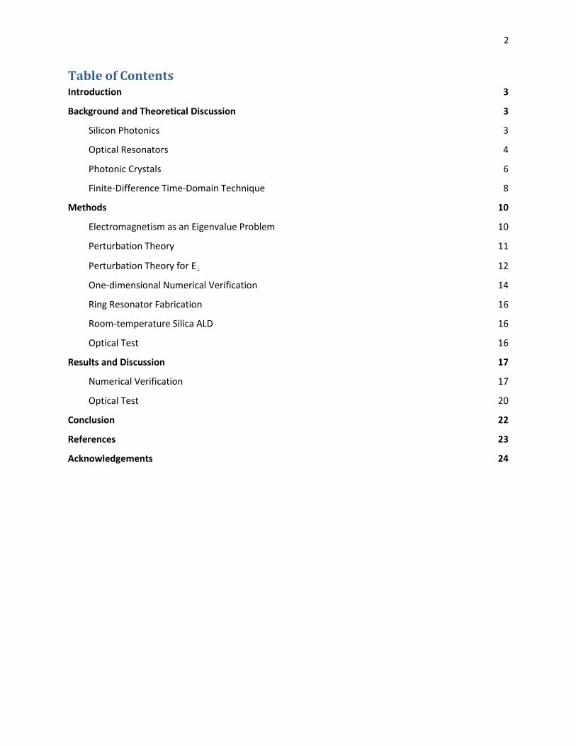
Table of Contents Introduction 3
Background and Theoretical Discussion 3
Silicon Photonics 3
Optical Resonators 4
Photonic Crystals 6
Finite-Difference Time-Domain Technique 8
Methods 10
Electromagnetism as an Eigenvalue Problem 10
Perturbation Theory 11
Perturbation Theory for E 12
One-dimensional Numerical Verification 14
Ring Resonator Fabrication 16
Room-temperature Silica ALD 16
Optical Test 16
Results and Discussion 17
Numerical Verification 17
Optical Test 20
Conclusion 22
References 23
Acknowledgements 24

3
Introduction Direct, high-sensitivity sensing of biomolecules would invite numerous applications in cost-effective
platforms for immunoassays and genetic sequencing. Current methods are generally low-sensitivity or
require fluorescent labeling of molecules prior to detection, which is expensive, time-consuming, and
often limits the testing to laboratories with specialized equipment. Significant effort has recently been
devoted to label-free sensing platforms, which eliminate the need for fluorophore attachment.1
Particularly exciting are biosensing platforms based on silicon photonics. Leveraging decades of
fabrication development from the microelectronics industry, it is possible to manufacture sensors that
rely on optical systems micromachined onto a common silicon wafer. The low cost and small size of
these systems, as well as their potential for integration with well-developed microfluidics technology,
would allow production of “lab-on-a-chip” devices that would bring advanced assay and diagnostic tools
directly to the point of care.
A common form of these sensors relies on the attachment of biomolecules to the surface of a resonant
cavity or waveguide; modulation in the cavity resonance or waveguide cutoff frequency caused by
biomolecule attachment indicates a detection event. Unfortunately, the optical influence of very small
molecule attachment, or essentially the addition of thin layers to a photonic structure, is intractable to
model directly with computational methods common in electromagnetism. While a common approach
is to average the refractive index of the material over a larger volume2, this can be inaccurate and does
not reflect the true sensing mechanism at work.
We seek to design a technique to model the addition of thin cladding layers of known refractive index
on an optical system with high index contrasts, as is common in silicon photonics. This will provide a
much improved method by which surface biosensors can be modeled, providing a fast and accurate
design metric for the analysis and further improvement of such systems.
Background and Theoretical Discussion
Silicon Photonics
The field of silicon photonics has grown tremendously since it was proposed over 40 years ago at Bell
Labs shortly after the birth of the laser.3 In one of its most common implementations, these devices
consist of structures patterned in the top (“active”)
crystalline silicon layer of a silicon-on-insulator wafer
(Figure 1). Light, launched into the edge of this thin
silicon layer, is confined via total internal reflection,
as the refractive index of silicon (n ≈ 3.5) is much
greater than that of silicon dioxide (n ≈ 1.5) or air (n
= 1). The thick buried oxide (BOX) layer sufficiently
isolates the light in the silicon active such that the
substrate’s effect can be ignored.
Figure 1: SOI raised strip waveguide cross-section (not to scale). Dimensions typical.

4
Waveguides can be formed in silicon by etching the active layer into a narrow strip. Much like in a
traditional metal waveguide, supported propagation modes in a silicon waveguide depend heavily on its
shape and size, the limiting condition now being the Fresnel conditions for total internal reflection
rather than the requirement that components of the electric and magnetic field vanish at the
conducting boundary.4 It can be shown that light can be almost completely confined inside a high-index
waveguide whose width is greater than the wavelength; however, these widths also support several
higher-order modes. Waveguides with narrower widths, such as silicon wire waveguides, will still guide
light, but will carry much of the energy in the external medium rather than in the waveguide itself.3 The
size of the waveguide can be selected to promote single- or few-mode operation at the wavelength of
interest; for many applications single-mode propagation is desirable since it reduces a number of losses
and complications with polarization sensitivity.5
Typical dimensions (220nm thickness, 450nm width) for single-mode TE01 waveguides operating near λ =
1.5μm are a tradeoff between suppression of higher-order modes and increased losses caused by
scattering from greater field interaction with sidewall surface roughness, an inherent artifact of the
reactive ion etch used to fabricate the waveguides.6 It is important to note that such waveguides carry
significant energy outside the waveguide itself, in evanescently decaying fields. The strong confinement
afforded by the high refractive index contrast of the silicon/air or silicon/oxide interface allows silicon
photonic systems to be miniaturized well beyond systems demonstrable in conventional optics;
lithographic patterning likewise makes the large-scale production of such optical circuits readily
possible.
Optical Resonators
One of the important elements of silicon photonic systems is the ring resonator. Bending a strip
waveguide into a ring creates a resonant cavity, much like that inside a free-space ring laser. Light
trapped inside the cavity will continue to circulate around the ring, accumulating a phase difference and
interfering with itself on multiple passes. Thus, only wavelengths that are an integer multiple of the
optical path length of the ring remain for any length of time.7
The frequency selectivity of these rings is ultimately limited by the decay of light from the cavity over
time, through a combination of surface scattering effects and bending losses. Making the analogy with a
mechanical oscillator, the selectivity of these rings can be expressed as a quality (Q) factor as a measure
of the degree of underdamping in the cavity:
The quality factor of a ring resonator grows exponentially with increasing ring radius as bending losses
decrease.8 Quality factor is directly related to the bandwidth of the resonance:

5
Where is the center frequency and is the FWHM of the resonance. It is in fact usually measured in
this manner using spectroscopic techniques, rather than directly measuring energy dissipation, though
the two methods are equivalent.
A strip waveguide routed alongside these rings (within a few hundred nanometers) can couple light into
and out of the ring through evanescent fields in a process directly analogous to quantum tunneling
between two potential wells. Light energy is built up in the ring cavity over many cycles, after which the
field in the ring resonator interferes with the field in the waveguide at its resonant wavelengths, causing
those frequencies to drop from the output spectrum of the strip waveguide, forming a very selective
filter (Figure 2, Figure 3).
Figure 2: Schematic of ring resonator with waveguide, top view.
Figure 3: Transmission spectrum of an ideal ring-resonator filter.
The addition of a waveguide alongside the ring reduces its quality factor (often significantly), since the
waveguide provides a loss mechanism for the energy stored in the ring. The new quality factor can be
expressed as:
Where is the quality factor of the isolated ring and is the quality factor of the coupling structure.
Another notable characteristic of the coupled-cavity filter is the spacing between subsequent resonance
zeros, or the free spectral range (FSR). The FSR is inversely proportional to the radius of the resonator,
and thus large resonators with high Q have somewhat low FSR.7 The free spectral range of the system is

6
important for many applications (e.g. telecommunications) where band spacing is a key consideration,
but does not play a significant role in the specification of photonic systems for biosensing.
It is useful to compare the ring resonator to its free-space counterpart, the Fabry-Perot or Gires-
Tournois etalon (Figure 4). In this free-space setup, light is coupled into the cavity through a partially-
reflecting mirror, then traverses some distance, reflecting off a mirror or series of mirrors with near
100% reflectance, and then exiting the cavity with an accumulated phase shift.7 This is equivalent to
light coupling into a ring evanescently, travelling around the ring for one or more passes, and then
exiting with a phase shift equal to the ring’s optical path length. The interference of this phase shift
with the light remaining in the waveguide causes the ring resonator’s spectral filtering. The advantage
of fabricating such a resonator on silicon is ease of design and mass-production without hand tuning
and, in the case of sensors, the ability to easily bring a very small volume of analyte into the high field
concentrations around the resonant cavity. The size of silicon ring resonators can also be several orders
of magnitude smaller than traditional etalon interferometers.
Figure 4: Gires-Tournois Etalon, in two equivalent representations.
Photonic Crystals
Photonic crystals are another important silicon photonic component that can act as a resonant filter
under some circumstances. Photonic crystals are materials with periodic dielectric functions in one or
more dimensions that, much like the periodic crystal lattice of a semiconductor does for electrons, can
maintain propagation without scattering of certain wavelengths of light in certain directions. They are
the ultimate designer material—by introducing an arbitrarily varying refractive index of some
periodicity, it is possible to engineer an entire optical band structure including, in some cases, a band
gap—a region of wavelengths where propagation in the crystal is not allowed in any direction (Figure
5).9 The simplest example of a photonic crystal is the famous Bragg mirror, where alternating layers of
different refractive index create an arbitrarily high-quality, though wavelength-selective mirror for one
direction of light propagation.

7
The particular implementation of photonic crystals with two dimensions of periodicity in the dielectric
function is particularly useful for integration on silicon. This structure uses a two-dimensional triangular
lattice of air holes machined into the
active silicon layer of an SOI wafer.
However, the 2D photonic crystal
alone does not confine light, as it
allows it to propagate freely along the
direction normal to the crystal plane.
Rather, the crystal is fabricated to be
of limited vertical extent, with total
internal reflection confining the light in
the out-of-plane direction. The
buffered oxide is usually etched away
to increase symmetry and field
confinement, leaving the silicon layer
suspended in air and creating a
“photonic crystal slab.”
Defect states, analogous to donor or
acceptor levels in an electronic band gap, can be created in photonic crystals by removing one or more
holes from the lattice (leaving them filled with silicon). A waveguide is created as an “W1” defect by
removing an entire row of holes from the lattice. Other common defects are “L1” and “L3” defects,
where one or three adjacent holes are removed from a single row of the lattice. These point defects act
as resonant cavities for frequencies in the photonic band gap and, much like ring resonators, can be
used as wavelength-selective filters.
We have previously developed a sensitive photonic crystal-based surface biosensor that measures small
changes in the transmission spectrum upon molecular binding (Figure 6). The desire to rigorously model
and predict the behavior of this sensor system—a very complex surface for biomolecule attachment—
motivates the present work: the development of a perturbation theory to model the effects of adding a
thin cladding layer to silicon photonic components.
Figure 5: (From Ref. 9) Band structure of a triangular lattice of air holes.

8
Figure 6: SEM of Photonic Crystal Sensor and corresponding transmission spectra. Colored curves denote spectra after attachment of a monolayer of 0.8nm molecules. MHD = multiple-hole-defect, the sensor design we describe in Ref. 2.
Finite-Difference Time-Domain Technique
The vast majority of photonics problems are too complex to admit analytical solutions. Instead, it is
necessary to turn towards computational modeling techniques to extract useful information about a
system. One of the most common computational techniques in electromagnetism is the finite-
difference time-domain (FDTD) method.
The FDTD method discretizes space into a cubic grid, maintaining arrays in memory of the electric and
magnetic field components at each point. In most implementations, the grid used is a Yee Lattice, in
which electric and magnetic field components are distributed in space such that every E component is
surrounded by four circulating H components and vice-versa (Figure 7).

9
Figure 7: (From Ref. 10) The Yee Lattice.10
Maxwell’s equations are then formulated in finite-difference form, and are stepped in time, updating
the electric and magnetic fields in a leapfrog fashion. This essentially runs a numerical experiment,
where, having defined field sources and a spatially-varying function of permittivity, it is possible to
determine field components anywhere in the simulation domain at any future time step.11
A significant disadvantage of FDTD is its extreme computational intensiveness. For accuracy, the spatial
grid resolution generally must be high enough to resolve features with several grid points.12 Most FDTD
techniques do not use nonuniform grids as they tend to introduce numerical error, so memory and
computational time is spent calculating fields across the entire domain even if only a small section has
structures justifying high resolution.11 Adding to the computational time is the issue of numerical
stability. FDTD simulations are bound by a Courant stability condition S:
Or, equivalently:
Time steps greater than this bound create an exponentially growing numerical wave introduced by
errors of the computational grid, namely, an unstable simulation.11 Together, these requirements make
the three-dimensional FDTD algorithm running time scale asymptotically with the fourth power of
resolution. For typical problem sizes, simulation times stretch into multiple days even on fast parallel
computers; modeling especially small features in large problem domains quickly becomes intractable.

10
Methods
Electromagnetism as an Eigenvalue Problem
The common task of modeling thin cladding layers on photonic elements falls into exactly the high-
resolution, large-domain problem case that makes direct numerical modeling impractical. To combat
the intractably long simulation times, I propose a hybrid computational-analytical technique that solves
a desired system for resonant frequencies at lower resolution and then applies an analytical
perturbation to that solution to find the resonant frequency shift caused by the added cladding layer.
We begin by formulating electromagnetism as an eigenvalue problem. We first restrict consideration to
the source-free case with linear, isotropic, dispersionless, nonmagnetic, and transparent materials.
While only a small subset of the general theory of electromagnetism, these limitations describe typical
photonic systems well and pose no real limitation for the theory. Specifically:
( ) ( ) ( )
Where ( ), the dielectric function, is a scalar function of position that does not depend on frequency or
the strength of the electric field.
This yields:
[ ( ) ( )]
( )
( )
( )
( ) ( ) ( )
Since Maxwell’s equations in this form are linear, we can leverage Fourier analysis to represent any
solution as a sum of Fourier modes:
( ) ∑ ( )
( ) ∑ ( )
Where ( ) is a “mode profile” at its resonant frequency ω.
With these stipulations, it is possible to formulate Maxwell’s equations as an eigenvalue problem:9
( ) (
)
( ) ( )
This can be shown to be both linear and Hermitian,9 allowing application of the same perturbation
theory that finds use in the mathematically similar problem in quantum mechanics.

11
Perturbation Theory
A naïve perturbation theory for photonics is well-established:9
( ) ( )
⟨ ( )| | ( )⟩
⟨ ( )| | ( )⟩
Where ( )is the unperturbed frequency, ( )is the corrected frequency, and ⟨ | | ⟩ is the Dirac
notation, where:
⟨ | | ⟩ ∫
Problematically, though, this first-order theory is only valid for small shifts in the permittivity ε, a
requirement clearly not valid for the present problem, where perturbations are often a change of 50%
or more in ε.
Instead, we take a suggestion from Johnson et al.13 and model the system as a shifting boundary
problem (Figure 8).
Figure 8: Setup for the cladding perturbation.
Here we add the layer ε2, extending from ε1 into ε3 between h1 (the original boundary) and h2. The one-
dimensional problem is considered for mathematical simplicity, and suffices for our applications.
Mathematically, ε(x) can be represented using Heaviside step functions:
( ) ( ) ( ) ( ) ( )
Or, defining the cladding thickness as t = h2 – h1 and changing variables to h = h1:
( ) ( ) ( ) ( ) ( )

12
The effect on the mode frequency ω of an infinitesimal change in thickness t can be expressed via a
form of the Hellman-Feynman theorem:13
( )
⟨ ( )| | ( )⟩
⟨ ( )| | ( )⟩
The only non-trivial part of this expression is the derivative dε/dt:
( ( ) ( ))
(( ) ( ))
( )
Where δ(x) denotes the Dirac delta function. The numerator of the Hellman-Feynman theorem then
evaluates to:
⟨ ( )|
| ( )⟩ ∬ ( )
This would at first appear to be a simple integral across the surface at x = h + t. Indeed, for electric fields
parallel (tangential) to the surface, this integral forms a valid perturbation theory for thin cladding
layers. However, electromagnetism requires that the electric displacement be continuous
across boundaries, thus making the electric field discontinuous across a discontinuous step in
permittivity. The integral above asks us to evaluate the electric field at that discontinuity, thus giving
undefined results for fields perpendicular to the interface.
Perturbation Theory for E
To develop a theory for the electric field components normal to the clad surface, we make the
observation that the expected solution for any sharp boundary is the limit of the solution for a smooth
transition as it is made progressively sharper. Moreover, that limit must be unique, so any self-
consistent method for smoothing the material boundaries will be equally valid. In that spirit, we
convolve the inverse of the epsilon function with an arbitrary smoothing function gs(x), essentially
creating a harmonic mean:
( ̅) ∫ ( ) ( )
Here, ( ) can be any nascent delta function (sinc, Gaussian, etc.), i.e. a function of unit integral,
centered at x = 0, which converges to the Dirac delta function as s → 0 (Figure 9). The precise choice of
function does not change the following derivation, where the smoothing function is simply a matter of
mathematical convenience.

13
Figure 9: Example smoothed epsilon function for Gaussian smoothing function and various values of s. Axis scales are arbitrary for demonstration of the smoothing concept.
Now differentiating with respect to t:
(̅ )
∫ ( ) ( )
(̅ ) ∫ ( )
( )
(̅ ) ∫ ( ) ( ) ( )
(̅ ) ∫ ( ) ( )
[ ( ) ( )]
(̅ ) ( )(
)
This result and that for fields parallel to the surface can be combined by considering ε(x) to be a tensor
quantity depending on the direction of the electric field:
( ) (
(̅ )
( )
( )
)
Thus, the numerator of the Hellman-Feynman theorem becomes:
⟨ ( )|
| ( )⟩ ∬[( |
( )| (
) ( ̅
( )) ] ( )
Note that here, when we take the limit s → 0, →̅ and ̅ ( )
( )
( )
. Since the electric
displacement is continuous across the boundary, it is now valid to evaluate the above expression
completely:

14
⟨ ( )|
| ( )⟩ ∫ [( |
( )| (
) (
( )) ]
And:
( )
⟨ ( )| | ( )⟩ ∫ [( |
( )| (
) (
( )) ]
This serves as a complete first-order perturbation theory for thin cladding layers on high index-contrast
surfaces.
One-dimensional Numerical Verification
With the mathematical theory now established, we seek an efficient method to test the results of this
perturbation method against direct simulation. In essence, we would like to compare the resonant
frequency calculated by application of the perturbation theory to an unclad system, where the
perturbation theory is used to account for the influence of the added cladding, to a direct simulation of
that system with cladding included. Problematically, however, almost all systems are too large to
directly simulate (that is indeed the very motivation for developing the perturbation theory).
In some sense, however, the particular system chosen for this comparison does not matter—once
shown correct, the perturbation theory should be correct for all systems of linear and isotropic dielectric
materials. Thus, we choose the simple system of an isolated silicon ring resonator in air, extending
infinitely in the direction of the ring’s axis of revolution, with thin cladding on its outer surface (Figure
10). Unlike most other systems, the isolated ring resonator has the advantage of perfect cylindrical and
z-axis translational symmetry, thus reducing an otherwise intractable three-dimensional problem to one
dimension (the radial distance r). Because the running time of the one-dimensional FDTD problem only
scales with the second power in resolution and the ring resonator requires a notably small
computational domain, this allows scaling of the resolution to astounding levels—a simulation with 2000
pixels across the width of the ring waveguide completes in less than one hour. This allows the
simulation to fully resolve even very thin cladding layers in direct simulation.

15
Figure 10: Diagram of isolated infinite ring resonator and corresponding 1d dielectric function. Dashed line indicates cladding location. Not to scale.
Specifically, we define a one-dimensional FDTD problem with continuous cylindrical symmetry
containing a silicon (ε = 11.68) ring waveguide of inner radius 1 and width 1 in the computational
domain (sizes are arbitrary since Maxwell’s equations are scale-invariant). A dipole electric field source
with field component out of the plane of revolution is placed just inside the ring, at 0.1 units from the
inside edge to excite all modes regardless of symmetry. A variable-thickness layer of silicon dioxide (ε =
3.9) is added to the outer edge of the ring. The entire structure is kept in a background of air with
absorbing perfectly matched layer (PML) boundaries to emulate an infinite simulation space.11
FDTD simulations were run using the open-source MIT Electromagnetic Equation Propagation (Meep)
software.14 To find resonant frequencies of the unclad cavity, fields were excited using a Gaussian
source envelope, exciting a range of frequencies centered at a normalized frequency of 0.12 (specified in
units of c / a, where a is the simulation’s characteristic length scale and the waveguide width). After
sources had decayed, harmonic inversion,15 a relative of Fourier analysis, was used to extract
frequencies and decay rates of the cavity modes.
Selecting a mode of interest, the simulation was run again with a narrow-bandwidth source at that
frequency to extract a single mode profile. To ensure that the mode profile was captured at a time
when all of the energy was in the electric field, the electric field profile was captured twenty times over
a single frequency cycle and the profile with the highest peak field was chosen as the true mode profile.

16
This field profile, along with the known resonant frequency, was then post-processed in Python to
calculate the perturbation correction.
To assess the validity of the theory over several cladding thicknesses, simulations were completed with
oxide cladding thicknesses varying from zero to one-quarter of the waveguide width and compared with
the corresponding perturbation of the unclad ring.
Ring Resonator Fabrication
With the theory established and numerically verified, we seek to validate it experimentally. To this end,
we fabricate and measure a complete silicon ring resonator filter. After baseline measurements, we
coat this resonator with a thin layer of silicon dioxide via atomic layer deposition, and measure the
resonant wavelength shift caused by this added cladding layer.
Ring resonators and coupled strip waveguides were fabricated on a silicon-on-insulator wafer (silicon
layer 220nm, 2μm BOX) by electron beam lithography followed by a reactive ion etch to transfer the
pattern into the silicon in a manner similar to Ref. 16.16 Samples were manually cleaved perpendicular
to the straight input/output waveguides to allow light to be coupled into them; no other coupling or
mode-matching method (grating couplers or nano-tapers) was used.
Room-temperature Silica ALD
Applying the thin cladding layer of oxide requires a method that is conformal, uniform, and easily-
controlled. Atomic layer deposition, where a precursor molecule is applied in vapor phase to the sample
surface and then catalyzed to form a single atomic layer of the target material, satisfies these
requirements. Traditionally, this process requires a carefully controlled vacuum chamber, as the process
gases are toxic and pyrophoric and require thermal or plasma sources to speed deposition. Vanderbilt
does not possess such equipment.
Instead, we adapt a recently-published silica atomic layer deposition technique that can be
accomplished in a test tube in air with liquid reagents.17 In a two-step process, samples are suspended
by copper wire in 15mm ID test tubes approximately 2 cm above 2mL of tetramethyl orthosilicate
(TMOS) for ten minutes, then 2 cm above 2mL of 30% ammonium hydroxide (NH4OH) for ten minutes.
The ammonia vapor catalyzes the hydrolysis of adsorbed TMOS to form silicon dioxide:
Si(OCH3)4 + 2 H2O → SiO2 + 4 CH3OH
While the method is sensitive to atmospheric conditions, particularly humidity, it produces a fairly
consistent layer of SiO2 for each two-step cycle, approximately 2nm in thickness as measured by
spectroscopic ellipsometry on silicon. We use three cycles, applying approximately 6nm of silica to the
waveguide surface.
Optical Test
The transmission spectra of the ring resonator filters were then measured using a straightforward
optical setup (Figure 11). Light from a tunable fiber laser is routed through a polarization controller and
then a polarization-maintaining tapered fiber to the test chip. Tapered fibers have a nominal spot size
of 2.5 μm and were mounted on an XYZ piezo stage for accurate alignment to the fabricated

17
waveguide. Output light was coupled into an identical fiber and into an optical power meter. The
fibers were aligned to maximize power transfer for a wavelength off the ring resonances.
Figure 11: Optical Test Setup. PC = Polarization Controller.
Under computer control, the laser wavelength was swept over its entire 1520nm-1570nm range at 0.25
nm/s and the transmitted power measured at each wavelength. Then a more detailed scan was
performed around one of the observed resonances: 1550nm-1555nm at a sweep rate of 0.05 nm/s. A
droplet of deionized water was applied to the chip surface for these measurements to improve coupling
from the waveguide to the adjacent ring. Measurements were normalized to a concurrent
measurement of an identical strip waveguide (without ring resonator).
Results and Discussion
Numerical Verification
The simulation of the infinite unclad ring resonator (Figure 10) yielded the field profile shown in Figure
12. X-axis coordinates are the distance radially outward from the center of the ring. As expected, the
peak field intensity is shifted toward the outside edge of the ring, confirming the presence of a
waveguide bend. Especially of note is the significant field energy present outside the physical extent of
the waveguide; it is this energy that interacts with the cladding layer, causing the frequency shift, and is
likewise responsible for the shift seen in photonic sensors.

18
Figure 12: Electric field profile in ring waveguide. Vertical blue lines indicate the physical extent of the waveguide. Radial position is scaled to the waveguide width a; vertical axis scale is arbitrary units. Note the significant field found outside of the ring.
A comparison of the resonant frequencies from both direct simulation and the perturbation theory for a
variety of cladding thicknesses is show in Figure 13. The naïve perturbation theory (accounting for a
small change in permittivity alone) is shown for comparison. Notably, the newly-developed
perturbation theory tracks the simulated result reasonably well even out to large (0.25 waveguide
width) cladding thicknesses. At this cladding level, the perturbation result (blue triangles) agrees with
the simulation to approximately 0.1% in frequency. Error does not exceed 0.2% over the entire range of
thicknesses tested. At a design wavelength of 1550nm and the equivalent physical ring of 182nm radius
with less than 30nm of cladding oxide, this error corresponds to a wavelength shift of 1-2nm. In
contrast, the naïve perturbation theory (red circles) under-adjusts for the cladding thickness by 25%, or
an error of 13nm at 1550nm. Frequency error of the new perturbation theory compared to direct
simulation, plotted versus cladding thickness, is shown in Figure 14.

19
Figure 13: Comparison of resonant frequencies calculated by direct simulation and perturbation techniques. a = width of ring waveguide.
Figure 14: Frequency error of the present perturbation theory vs. direct simulation.

20
Optical Test
Spectroscopy measurements of transmitted light through the fabricated ring resonator filter display the
expected periodic resonance dips (Figure 15). This confirms that the ring resonator was fabricated
correctly and that light is effectively coupling between the bus waveguide and ring. Observations from
an IR camera focused on the device likewise confirm light coupling into and scattering from the ring at
resonance.
Figure 15: Transmission spectrum of the ring resonator prior to oxide cladding. Note the five evenly-spaced dips in transmission at resonance.
A more detailed scan of the resonance near 1550nm is shown in Figure 16. Silicon dioxide deposition
(approximately 6nm thickness) causes a redshift of 0.12nm. Reassuringly, this shift is in the proper
direction, but it is significantly smaller than predicted by the one-dimensional models shown earlier.
This can be explained by several factors.

21
Figure 16: Transmission spectra of one ring resonance before and after oxide cladding. The oscillating pattern off-resonance is believed to be a Fabry-Perot effect from the two reflecting ends of the strip waveguide. The wavelength shift is 0.12 nm.
First, the fabricated rings were measured in a water background instead of the air background of the
simulations. Because the refractive index contrast between oxide and water is several times smaller
than that between oxide and air, the expected perturbation decreases similarly. While we found the
water droplet necessary to ensure sufficient coupling to the rings, there is no fundamental reason why
this needs to be the case. Further fabrication refinement should allow coupling in air and a
correspondingly larger wavelength shift.
Additionally, the ring simulated for theoretical verification (results in Figures 12-14) is significantly
smaller than the one fabricated. A larger ring is convenient experimentally because of its higher Q-
factor and correspondingly sharper resonance. As a consequence of the larger radius and wider
waveguide, however, bending losses are reduced and less field energy is carried outside the waveguide
in the cladding layer. Because the frequency perturbation is proportional to the square of the field at
the waveguide surface, a drop in field intensity in this region compared to the verification system
creates a correspondingly smaller wavelength shift.
Reassuringly, a one-dimensional simulation with parameters set to model the fabricated ring resonator
agrees far more closely with the experimental results (a simulated shift of 0.09nm compared to an
experimental shift of 0.12nm). We posit that, given the close agreement between direct simulation and
perturbation theory in the model system and the similarly close agreement between direct simulation
and experimental results for the fabricated ring, that perturbation theory will continue to be valid for
such systems.

22
A remaining obstacle in a full implementation and verification of this theory is the possible disparity
between one-dimensional simulations and three-dimensional experiment. While the theory is valid for
fully three-dimensional simulations, applying it to such systems involves an extra layer of complexity, as
the electric field must be interpolated from a low-resolution simulation grid to the points at the cladding
surface and a numerical surface integral taken in three-dimensional space. The additional code to apply
the perturbation theory to results of three-dimensional simulations has not yet been developed, though
it is a clear next step in the confirmation and application of this theory.
Conclusion We have successfully developed a compact first-order perturbation theory to model the attachment of
thin layers of known refractive index on a high index-contrast boundary surface, such as is often found
in silicon photonics. This theory is valid for all electric field components and arbitrary choice of index,
and can be applied as a simple post-processing correction given both a mode profile and center
wavelength of the optical resonance of interest.
Results calculated by this theory match closely to direct simulations of oxide cladding on a model silicon
ring-resonator system. Experimental results likewise show a tentative confirmation of the theory,
though further work is necessary to closely align experimental and theoretical results.
Particularly, an immediate concern is the adaptation of the perturbation theory to a low-resolution, fully
three-dimensional structure. This requires an interpolation routine and surface integration code that,
while not a difficult research problem, would significantly improve the usability of the theory and
confidence in its results. Such an extension would allow the theory to be applied to model more
complex sensing systems, serving as a powerful metric by which to judge the quality of such designs.
We hope that such an understanding will lead to the development of higher-quality devices for sensitive
biomolecule detection and the consequent ability to bring sophisticated tests directly to the end-user.

23
References 1 Fan, Xudong, Ian M. White, Siyka I. Shopova, Hongying Zhu, Jonathan D. Suter, and Yuze Sun. “Sensitive
optical biosensors for unlabeled targets: a review.” Analytica Chimica Acta 620 (2008): 8-26. 2 Kang, Christopher, Christopher T. Phare, Yurii A. Vlasov, Solomon Assefa, and Sharon M. Weiss.
“Photonic crystal slab sensor with enhanced surface area.” Optics Express 18 (2010): 27930-7. 3 Miller, Stewart E. “Integrated Optics: An Introduction.” Bell System Technical Journal 48 (1969): 2059-
69. 4 Griffiths, David J. Introduction to Electromagnetism. Upper Saddle River, NJ: Prentice Hall, 1999, p. 405. 5 Dulkeith, Eric, Fengnian Xia, Laurent Schares, William M. J. Green, and Yurii A. Vlasov. “Group index
and group velocity dispersion in silicon-on-insulator photonic wires.” Optics Express 14 (2006): 3853-63.
6 Lee, K. K., D. R. Lim, H. C. Luan, A. Agarwal, J. Foresi, and L. C. Kimerling, "Effect of size and roughness on light transmission in a Si/SiO2 waveguide: Experiments and model." Applied Physics Letters 77 (2000): 2258-2258.
7 Heebner, John, Rohit Grover, and Tarek Ibrahim. Optical Resonators: Theory, Fabrication, and Applications. London: Springer-Verlag, 2008.
8 Marcatili, E.A.J. “Bends in Optical Dielectric Guides.” Bell System Technical Journal 48 (1969): 2103-32. 9 Joannopoulos, John D., Steven G. Johnson, Joshua N. Winn, and Robert D. Meade. Photonic Crystals:
Molding the Flow of Light, 2nd ed. Princeton, NJ: Princeton University Press, 2008. 10 Johnson, Steven G. Yee-cube.svg. From Wikipedia: http://en.wikipedia.org/wiki/File:Yee-cube.svg.
Licensed under a Creative Commons CC-BY-SA License, 2005. 11 Taflove, Allen, and Susan C. Hagness. Computational Electrodynamics: The Finite-Difference Time-
Domain Method, 2nd ed. Boston: Artech House, 2000. 12 Johnson, Steven G. Meep Tutorial. From MIT Nanostructures and Computation Wiki: http://ab-
initio.mit.edu/wiki/index.php/Meep_Tutorial. 13 Johnson, Steven G., M. Ibanescu, M.A. Skorobogatiy, O. Weisberg, J.D. Joannopoulos, and Y. Fink.
“Perturbation theory for Maxwell’s equations with shifting material boundaries.” Physical Review E 65 (2002): 066611.
14 Oskooi, Ardavan F., David Roundy, Miahi Ibanescu, Peter Bermel, J.D. Joannopoulos, and Steven G. Johnson. “MEEP: A flexible free-software package for electromagnetic simulations by the FDTD method.” Computer Physics Communications 181 (2010): 687-702.
15 Mandelshtam, V.A. and H.S. Taylor. “Harmonic inversion of time signals.” Journal of Chemical Physics 107 (1997): 6756-69.
16 Nag, Joyeeta, Judson D. Ryckman, Michael T. Hertkorn, Bo K. Choi, Richard F. Haglund, Jr., and Sharon M. Weiss. “Ultrafast compact silicon-based ring resonator modulators using metal-insulator switching of vanadium dioxide.” Proc. SPIE 7597, 759710 (2010).
17 Hatton, Benjamin, Vladimir Kitaev, Doug Perovic, Geoff Ozin, and Joanna Aizenberg. “Low-temperature synthesis of nanoscale silica multilayers—atomic layer deposition in a test tube.” Journal of Materials Chemistry 20 (2010): 6009-13.

Acknowledgements I am very grateful to Sharon Weiss for her guidance and assistance throughout the project. I would like
to acknowledge Judson Ryckman and Chris Kang for device fabrication and assistance with the physical
measurement setup. I also thank my entire research group, family, and friends for their support
throughout the project. Finally, I acknowledge funding support in part from the National Science
Foundation (Grant# EECS0925642).
Additionally, I would like to sincerely thank Richard Haglund, Norman Tolk, and Charles Maguire for
serving on my committee of independent examiners and for their support throughout my time at
Vanderbilt.