Perovskite Tandem Solar Cells -...
18
www.advenergymat.de PROGRESS REPORT 1602761 (1 of 18) © 2017 WILEY-VCH Verlag GmbH & Co. KGaA, Weinheim Perovskite Tandem Solar Cells Niraj N. Lal,* Yasmina Dkhissi, Wei Li, Qicheng Hou, Yi-Bing Cheng, and Udo Bach* DOI: 10.1002/aenm.201602761 1. Introduction Perovskite solar cells have developed faster in efficiency than any other photovoltaic (PV) technology in history. [1,2] With sun- shine-to-electricity conversion efficiencies below 4% in 2009, single-junction perovskite solar cells now demonstrate certi- fied efficiencies that rival all other thin-film PV technologies, reaching above 22% in 2016. [3] Accompanying this stunning The meteoric rise of perovskite single-junction solar cells has been accom- panied by similar stunning developments in perovskite tandem solar cells. Debuting with efficiencies less than 14% in 2014, silicon–perovskite solar cells are now above 25% and will soon surpass record silicon single-junction efficiencies. Unconstrained by the Shockley–Quiesser single-junction limit, perovskite tandems suggest a real possibility of true third-generation thin-film photovoltaics; monolithic all-perovskite tandems have reached 18% efficiency and will likely pass perovskite single-junction efficiencies within the next 5 years. Inorganic–organic metal–halide perovskites are ideal candidates for inclusion in tandem solar cells due to their high radiative recombination effi- ciencies, excellent absorption, long-range charge-transport, and broad ability to tune the bandgap. In this progress report, the development of perovskite tandem cells is reviewed, with presentation of their key motivations and challenges. In detail, it presents an overview of recombination layer mate- rials, bandgap-tuneability, transparent contact architectures, and perovskite compounds for use in tandems. Theoretical estimates of efficiency for future tandem and triple-junction perovskite cells are presented, outlining roadmaps for future focused research. Solar Cells Dr. N. N. Lal, Dr. Y. Dkhissi, Dr. W. Li, Q. Hou, Prof. Y.-B. Cheng, Prof. U. Bach ARC Centre of Excellence in Exciton Science Department of Materials Science and Engineering Monash University Victoria 3800, Australia E-mail: [email protected]; [email protected] Dr. N. N. Lal, Prof. U. Bach CSIRO Clayton Victoria 3169, Australia Prof. U. Bach The Melbourne Centre for Nanofabrication Clayton, Victoria 3169, Australia Prof. Y.-B. Cheng State Key Laboratory of Advanced Technology for Materials Synthesis and Processing Wuhan University of Technology Wuhan 430070, China growth has been the development of per- ovskite tandem solar cells; debuting at less than 14% in 2014, [4] silicon–perovskite four-terminal tandems now demonstrate efficiencies above 25% [5] with two-ter- minal efficiencies of 23.6%. [6] Perovskite– perovskite tandems utilising low-bandgap perovskite materials for the bottom cell now have four-terminal efficiencies above 20% [7] and two-terminal efficiencies above 18% [8] (Figure 1). Tandem solar cells allow higher effi- ciencies than single-junction solar cells by better utilising the energy of short-wave- length photons in the spectrum of sun- light. Top cells comprising a high-bandgap semiconductor generate photocurrent at high voltage from the short-wavelength part of the solar spectrum. Longer-wave- length light, beyond the bandgap of the top cell, is transmitted to an underlying bottom cell comprising a lower-bandgap semiconductor with broad absorption coefficient. The efficiency potential of tandem cells makes them the most likely candidate to continue the remarkable reductions in PV module price for decades to come. [9] Herein, we review the field of tandem solar cells based on a new PV material class of inorganic–organic lead–halide per- ovskites. Perovskites are an ideal candidate for inclusion in tandem solar cells due to their high radiative recombination efficiencies, excellent absorption and charge-transport charac- teristics, and their broad ability to tune the bandgap. [24–28] We present these key motivations for the perovskite-tandem archi- tecture alongside their challenges, outlining a roadmap for future focused research. This review article is organised as follows: In Section 2 we outline the case for tandem solar cells in both two- and four- terminal configurations, and present their efficiency evolu- tion to date. Theoretical efficiency limits are discussed and we review current record perovskite-tandem devices. Section 3 identifies possibilities for tandem cells that are unique to inor- ganic–organic metal–halide-perovskite materials, particularly due to their bandgap-tuneability and luminescence efficiency. The section also presents the optical and electrical require- ments of any future successful perovskite tandem solar cell, and the challenges of stability and longevity. Section 4 reviews the critical role of transparent contacts and recom- bination layers in tandem solar cells. It presents the state-of- the-art transmittances and sheet resistances (with and without metallization) of current transparent contact materials, and reviews candidates for the intermediate recombination layer in Adv. Energy Mater. 2017, 1602761
Transcript of Perovskite Tandem Solar Cells -...
www.advenergymat.de
PROGRESS REPORT
1602761 (1 of 18) © 2017 WILEY-VCH Verlag GmbH & Co. KGaA, Weinheim
Perovskite Tandem Solar Cells
Niraj N. Lal,* Yasmina Dkhissi, Wei Li, Qicheng Hou, Yi-Bing Cheng, and Udo Bach*
DOI: 10.1002/aenm.201602761
1. Introduction
Perovskite solar cells have developed faster in efficiency than any other photovoltaic (PV) technology in history.[1,2] With sun-shine-to-electricity conversion efficiencies below 4% in 2009, single-junction perovskite solar cells now demonstrate certi-fied efficiencies that rival all other thin-film PV technologies, reaching above 22% in 2016.[3] Accompanying this stunning
The meteoric rise of perovskite single-junction solar cells has been accom-panied by similar stunning developments in perovskite tandem solar cells. Debuting with efficiencies less than 14% in 2014, silicon–perovskite solar cells are now above 25% and will soon surpass record silicon single-junction efficiencies. Unconstrained by the Shockley–Quiesser single-junction limit, perovskite tandems suggest a real possibility of true third-generation thin-film photovoltaics; monolithic all-perovskite tandems have reached 18% efficiency and will likely pass perovskite single-junction efficiencies within the next 5 years. Inorganic–organic metal–halide perovskites are ideal candidates for inclusion in tandem solar cells due to their high radiative recombination effi-ciencies, excellent absorption, long-range charge-transport, and broad ability to tune the bandgap. In this progress report, the development of perovskite tandem cells is reviewed, with presentation of their key motivations and challenges. In detail, it presents an overview of recombination layer mate-rials, bandgap-tuneability, transparent contact architectures, and perovskite compounds for use in tandems. Theoretical estimates of efficiency for future tandem and triple-junction perovskite cells are presented, outlining roadmaps for future focused research.
Solar Cells
Dr. N. N. Lal, Dr. Y. Dkhissi, Dr. W. Li, Q. Hou, Prof. Y.-B. Cheng, Prof. U. BachARC Centre of Excellence in Exciton Science Department of Materials Science and EngineeringMonash UniversityVictoria 3800, AustraliaE-mail: [email protected]; [email protected]. N. N. Lal, Prof. U. BachCSIRO ClaytonVictoria 3169, AustraliaProf. U. BachThe Melbourne Centre for NanofabricationClayton, Victoria 3169, AustraliaProf. Y.-B. ChengState Key Laboratory of Advanced Technology for Materials Synthesis and ProcessingWuhan University of TechnologyWuhan 430070, China
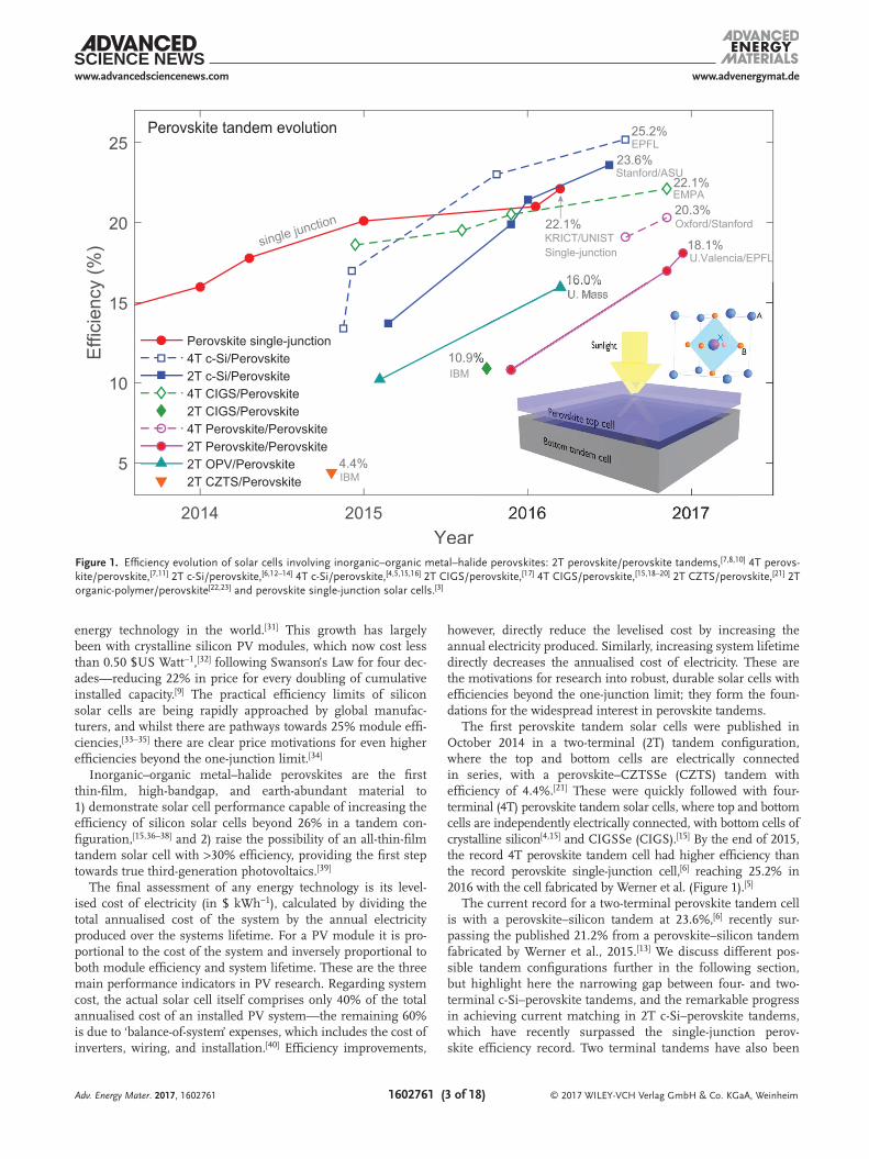
growth has been the development of per-ovskite tandem solar cells; debuting at less than 14% in 2014,[4] silicon–perovskite four-terminal tandems now demonstrate efficiencies above 25%[5] with two-ter-minal efficiencies of 23.6%.[6] Perovskite–perovskite tandems utilising low-bandgap perovskite materials for the bottom cell now have four-terminal efficiencies above 20%[7] and two-terminal efficiencies above 18%[8] (Figure 1).
Tandem solar cells allow higher effi-ciencies than single-junction solar cells by better utilising the energy of short-wave-length photons in the spectrum of sun-light. Top cells comprising a high-bandgap semiconductor generate photocurrent at high voltage from the short-wavelength part of the solar spectrum. Longer-wave-length light, beyond the bandgap of the top cell, is transmitted to an underlying bottom cell comprising a lower-bandgap semiconductor with broad absorption coefficient. The efficiency potential of tandem cells makes them the most likely
candidate to continue the remarkable reductions in PV module price for decades to come.[9]
Herein, we review the field of tandem solar cells based on a new PV material class of inorganic–organic lead–halide per-ovskites. Perovskites are an ideal candidate for inclusion in tandem solar cells due to their high radiative recombination efficiencies, excellent absorption and charge-transport charac-teristics, and their broad ability to tune the bandgap.[24–28] We present these key motivations for the perovskite-tandem archi-tecture alongside their challenges, outlining a roadmap for future focused research.
This review article is organised as follows: In Section 2 we outline the case for tandem solar cells in both two- and four-terminal configurations, and present their efficiency evolu-tion to date. Theoretical efficiency limits are discussed and we review current record perovskite-tandem devices. Section 3 identifies possibilities for tandem cells that are unique to inor-ganic–organic metal–halide-perovskite materials, particularly due to their bandgap-tuneability and luminescence efficiency. The section also presents the optical and electrical require-ments of any future successful perovskite tandem solar cell, and the challenges of stability and longevity. Section 4 reviews the critical role of transparent contacts and recom-bination layers in tandem solar cells. It presents the state-of-the-art transmittances and sheet resistances (with and without metallization) of current transparent contact materials, and reviews candidates for the intermediate recombination layer in
Adv. Energy Mater. 2017, 1602761

www.advenergymat.dewww.advancedsciencenews.com
© 2017 WILEY-VCH Verlag GmbH & Co. KGaA, Weinheim1602761 (2 of 18)
two-terminal tandems. Section 5 outlines the progress and potential of perovskite–perovskite tandems and presents a roadmap for future investigation towards large-area, low-cost solar electricity beyond 30% efficiency.
Perovskite tandems have been reviewed previously;[29,30] we expand on these to include more detailed analysis of a range of areas, including perovskite–perovskite tandems, mono-lithic-tandem recombination layers, transparent contacts with metallization, and a broader scope for future triple-junction and commercial perovskite tandem solar cells.
In summary, this review highlights the following:
1.1. Review Summary
Perovskites are an outstanding material for tandem solar cells, offering strong absorption, excellent charge-carrier transport, tuneability in the bandgap from 1.2–2.2 eV, sharp absorption band-edge, and low levels of parasitic absorption.
Perovskite–silicon monolithic tandems have reached 23.6%[6] efficiency with four-terminal tandem efficiencies beyond 25%.[5] A perovskite–silicon tandem surpassing the ‘break-even’ silicon single-junction efficiency of 26% is likely to be achieved by the year 2020.
Perovskite–perovskite tandems have demonstrated 20.3% four-terminal efficiency[7] and monolithic efficiency of 18.1%.[8] Perovskite–perovskite tandem efficiencies are ex-pected to surpass record perovskite single-junction efficien-cies before 2020, with efficiencies greater than 26% expected before 2030.
Critical issues for future progress are identified as:
Fabrication of compatible recombination layers with mini-mal voltage and optical losses, without the use of indium;
Control of light within the device including transparency of the top electrode, wavelength-selective light-trapping, and reduced reflection;
Cell stability that allows a performance guarantee of 80% output-efficiency for 25 years, and the fabrication of cells with non-toxic and earth-abundant materials.
We identify the following areas for interest and targeted future research:
Reduction of Voc loss-in-potential for high-bandgap perovskites.
Efficient stable perovskite semiconductors with low bandgap <1.1 eV
Fabrication-compatible transparent conductors and recom-bination layers without indium
Wavelength-selective light-trapping techniques with excel-lent long-pass transmission.
Perovskite compounds for selective transport, transpar-ent contact, and recombination layers in integrated multi-junction perovskite devices.
2. Perovskite Tandem Progress and Scope
Solar photovoltaic installations have grown at a compound rate of 44% per annum for the past 10 years, faster than any other
Niraj Lal is a postdoctoral researcher at Monash University and CSIRO. He graduated as a Gates Scholar with a Ph.D. in physics from the Cavendish Laboratory, University of Cambridge in 2012 with Prof. Jeremy Baumberg. Prior to his Ph.D. he was a tuna long-line fishing deckhand, bicycle courier, and a travelling
science presenter to school children across Western Australia. Nij has written two children’s books about science, is the founder of TheKnews.org and is passionate about environmental sustainability and science outreach.
Yasmina Dkhissi is a postdoc-toral researcher at Monash University where she works on the development of perov-skite/silicon tandem solar cells. She received a Ph.D. degree from the University of Melbourne for her work on flexible thin-film solar cells. Carried out in close collabora-tion with Monash University and the CSIRO, her research
looked in particular at device-fabrication techniques and at practical industrial concerns such as the reproducibility, manufacturing processability, and the stability of perovskite solar cells.
Udo Bach is a full professor at Monash University, Deputy Director of the ARC Centre of Excellence in Exciton Science and an ANFF-VIC Technology Fellow at the Melbourne Centre of Nanofabrication (MCN). He received his Ph.D. from the Swiss Federal Institute of Technology (EPFL, Switzerland) working in the research group of
Prof. Michael Grätzel and worked for 3 years in a technology start-up company in Dublin (Ireland). Subsequently he spent 15 months as a postdoc in the group of Prof. Paul Alivisatos at UC Berkeley (USA) before moving to Monash University in November 2005 to establishing his own research group. He is involved in fundamental and applied research in the area of perovskite and dye-sensitized solar cells with additional activities in the area of nanofabrication, nanopar-ticle self-assembly and combinatorial photovoltaic materials discovery.
Adv. Energy Mater. 2017, 1602761
www.advenergymat.dewww.advancedsciencenews.com
© 2017 WILEY-VCH Verlag GmbH & Co. KGaA, Weinheim1602761 (3 of 18)
energy technology in the world.[31] This growth has largely been with crystalline silicon PV modules, which now cost less than 0.50 $US Watt-1,[32] following Swanson’s Law for four dec-ades—reducing 22% in price for every doubling of cumulative installed capacity.[9] The practical efficiency limits of silicon solar cells are being rapidly approached by global manufac-turers, and whilst there are pathways towards 25% module effi-ciencies,[33–35] there are clear price motivations for even higher efficiencies beyond the one-junction limit.[34]
Inorganic–organic metal–halide perovskites are the first thin-film, high-bandgap, and earth-abundant material to 1) demonstrate solar cell performance capable of increasing the efficiency of silicon solar cells beyond 26% in a tandem con-figuration,[15,36–38] and 2) raise the possibility of an all-thin-film tandem solar cell with >30% efficiency, providing the first step towards true third-generation photovoltaics.[39]
The final assessment of any energy technology is its level-ised cost of electricity (in $ kWh-1), calculated by dividing the total annualised cost of the system by the annual electricity produced over the systems lifetime. For a PV module it is pro-portional to the cost of the system and inversely proportional to both module efficiency and system lifetime. These are the three main performance indicators in PV research. Regarding system cost, the actual solar cell itself comprises only 40% of the total annualised cost of an installed PV system—the remaining 60% is due to ‘balance-of-system’ expenses, which includes the cost of inverters, wiring, and installation.[40] Efficiency improvements,
however, directly reduce the levelised cost by increasing the annual electricity produced. Similarly, increasing system lifetime directly decreases the annualised cost of electricity. These are the motivations for research into robust, durable solar cells with efficiencies beyond the one-junction limit; they form the foun-dations for the widespread interest in perovskite tandems.
The first perovskite tandem solar cells were published in October 2014 in a two-terminal (2T) tandem configuration, where the top and bottom cells are electrically connected in series, with a perovskite–CZTSSe (CZTS) tandem with efficiency of 4.4%.[21] These were quickly followed with four- terminal (4T) perovskite tandem solar cells, where top and bottom cells are independently electrically connected, with bottom cells of crystalline silicon[4,15] and CIGSSe (CIGS).[15] By the end of 2015, the record 4T perovskite tandem cell had higher efficiency than the record perovskite single-junction cell,[6] reaching 25.2% in 2016 with the cell fabricated by Werner et al. (Figure 1).[5]
The current record for a two-terminal perovskite tandem cell is with a perovskite–silicon tandem at 23.6%,[6] recently sur-passing the published 21.2% from a perovskite–silicon tandem fabricated by Werner et al., 2015.[13] We discuss different pos-sible tandem configurations further in the following section, but highlight here the narrowing gap between four- and two-terminal c-Si–perovskite tandems, and the remarkable progress in achieving current matching in 2T c-Si–perovskite tandems, which have recently surpassed the single-junction perov-skite efficiency record. Two terminal tandems have also been
Adv. Energy Mater. 2017, 1602761
Figure 1. Efficiency evolution of solar cells involving inorganic–organic metal–halide perovskites: 2T perovskite/perovskite tandems,[7,8,10] 4T perovs-kite/perovskite,[7,11] 2T c-Si/perovskite,[6,12–14] 4T c-Si/perovskite,[4,5,15,16] 2T CIGS/perovskite,[17] 4T CIGS/perovskite,[15,18–20] 2T CZTS/perovskite,[21] 2T organic-polymer/perovskite[22,23] and perovskite single-junction solar cells.[3]

www.advenergymat.dewww.advancedsciencenews.com
© 2017 WILEY-VCH Verlag GmbH & Co. KGaA, Weinheim1602761 (4 of 18)
fabricated with CIGS (10.9%[17]), organic (16.0%[23]), and per-ovskite low-bandgap bottom cells (18.1%[8]), discussed further below.
The most likely first route to market for perovskite solar cells is predicted as an accompanying tandem layer for a premium silicon solar cell module,[34] though it is critical to note that to improve the efficiency of an existing excellent silicon solar cell requires efficiencies above ≈20% from the perovskite cell.[15,36–38] Serious questions should be asked about the long-term feasibility of the approach of combining a PV technology with excellent stability but high intrinsic material cost (crystal-line silicon) with a PV technology with as-yet low stability but cheap intrinsic material cost (perovskite).[41] When perovskite materials demonstrate the efficiency and stability required for inclusion in a commercial silicon tandem module, it is likely they will be efficient and stable enough for deployment as either a standalone perovskite solar module, or as a high-effi-ciency perovskite–perovskite tandem.[21,30]
Perovskite–perovskite tandems were first fabricated in 2015 with a 2T configuration of identical top and bottom cells.[10] In mid-2016, the first 4T perovskite–perovskite tandem was published with 19.1% efficiency,[11] and in late 2016, Eperon et al. demonstrated record 2T and 4T perovs-kite–perovskite tandems with ideal matched bandgaps, at 17.0% and 20.3%, respectively.[7] This was recently furthered by Forgács et al. in December 2016, demonstrating 18.1% 2T perovskite/perovskite tandem efficiency, though we note here that this efficiency was unstabilised and measured only in the reverse-scanning direction from open-circuit to short-cir-cuit.[8] Whilst the efficiency under forward scanning still pro-vides a new record (at 17.4%), further record cells will benefit from adhering to the guidelines in correct perovskite cell-effi-ciency measurement at steady-state, outlined by Christians et al. in 2015.[42]
With conservative extrapolation of recent progress (>2% absolute efficiency increase per year for the majority of per-ovskite tandem technologies, Figure 1), we expect perovskite–perovskite tandem efficiencies to surpass record perovskite single-junction efficiencies before 2020. Whilst efficiency gains are of course harder to achieve closer to the single-junction limit, we note that perovskite single-junction development will also benefit tandem development unconstrained by the single-junction limit. Further extrapolation conservatively predicts perovskite–perovskite tandem efficiencies greater than 26% before 2030. We discuss the progress and opportunities for per-ovskite–perovskite tandems in detail in Section 5, but note here it is a future research area of significant interest to the photo-voltaic community.
2.1. Tandem Configurations
Tandem solar cells allow higher efficiencies than single-junc-tion devices by absorbing higher-energy solar photons in a high-bandgap top cell material where it can generate photo-current with higher voltage than the underlying solar cell with lower bandgap but broader absorption coefficient.
There are four main tandem solar cell configurations, each with varying degrees of optical and electrical independence.
Four-terminal (4T) configurations comprise top and bottom cells that are independently connected; both cells are required to be complete devices (fabricated with front and rear con-tacts), which are then connected externally to combine the top and bottom cell power output. Four terminal tandem cells are unconstrained by current-matching and have achieved the highest perovskite tandem efficiencies to date (perovskite:c-Si 25.2%[5]). 4T tandems include designs where longer-wavelength sunlight passes through the top-cell to the bottom cell (Figure 2a), or reflected to an adjacent bottom cell (Figure 2d). Series-parallel tandem (SPT) configurations (Figure 2c) com-bine strings of top and bottom cells separately before con-nection of the voltage-matched strings in parallel, providing a practical method for combining the two cell power outputs at similar performance to 4T configurations in annual energy yield.[43,44]
The most desirable and challenging configuration is that of series-connected monolithic tandems (Figure 2b); desirable because they allow both simpler electrical connection and omit the need for rear and front electrodes for the top and bottom cell, respectively. Challenges to fabricate efficient 2T devices include i) current-matching between the top and bottom cell, ii) fabrica-tion of recombination layers with minimal losses between the cells, and iii) optical management within the tandem. We dis-cuss these challenges further in Sections 3 and 4.
2.2. Efficiency Progress and Limits
The theoretical efficiency limit for a tandem solar cell under unconcentrated sunlight (AM1.5G spectrum) is 47% (Figure 3a),[45,46] markedly higher than the Shockley-Quiesser limit of 31% for single-junction cells under unconcentrated sunlight.[47,48] We examine both unconstrained 4T theoretical efficiencies (Figure 3a) and 2T tandems (Figure 3b), using the results from Kurtz et al. employing a GaAs top-cell with opti-mised thickness for current-matching.[49]
For both the four- and two-terminal tandem contour maps, we see a broad peak in the theoretical maxima: 4T tandem effi-ciencies peak at 47% for a top/bottom cell bandgap pairing of 1.62/0.95 eV, and 2T at 39% for 1.72/1.14 eV, but efficiencies within 10% of the peak can be found +/-0.1 eV either side of the peak in both directions. The reduced peak 2T efficiency of 39% compared to the 4T value of 47% is due to Kurtz’s model-ling of GaAs as the top-cell material of the 2T tandem, with non-ideal Jo;[49] though the trend for perovskite cells remains the same. We see particularly low sensitivity for 2T tandems when the bottom cell thickness is allowed to be varied for current-matching (Figure 3b). Connecting submodules of two terminal tandems (SPT) also affords greater flexibility in cell bandgap choice, with appropriate combinations matching performance of four-terminal independently-connected devices.[43,44]
Current prevalent inorganic–organic lead–halide perovskites have bandgaps (1.55–2.2 eV) ideally suited to being the top cell of a tandem with any of the lower bandgap cells comprising crystalline silicon, CIGS or CZTS. Recent perovksite blends incorporating tin, such as the FA0.75Cs0.25Sn0.5Pb0.5I3 blend fab-ricated by Eperon et al. (1.2 eV)[7] and MA0.5FA0.5Pb0.75 Sn0.25I3
Adv. Energy Mater. 2017, 1602761

www.advenergymat.dewww.advancedsciencenews.com
© 2017 WILEY-VCH Verlag GmbH & Co. KGaA, Weinheim1602761 (5 of 18)
by Yang et al. (1.33 eV),[11] also demonstrate the ability to per-form as the low-bandgap material of a tandem bottom cell. We identify here also the significant potential for investigation of perovskite compounds of even lower bandgap (0.95–1.15 eV) as the bottom cell of a two or four terminal perovskite–perovskite multijunction cell (Section 5). We discuss bandgap tuneability of perovskite materials further in Section 3.
The theoretical efficiency contour maps for varying top- and bottom-cell bandgaps (Figure 3), provide incentive and instruction for further optimisation of perovskite materials; current record efficiencies (overlayed on the graph) are less than 60% of their theoretical maxima. Even allowing for una-voidable optical and electrical losses in nontheoretical systems, there is significant space for further improvement.
With conservative extrapolation of the historical progress of perovskite efficiencies over the past decade, we expect a 4T perovskite–silicon tandem beyond the ‘break-even’ efficiency of 26% to be achieved in the laboratory by the year 2020, with 2T perovskite–silicon cells following by 2025. Perovskite–per-ovskite 4T tandem efficiencies are expected to surpass record perovskite single-junction efficiencies before 2020, with 2T effi-ciencies greater than 26% expected before 2030.
2.3. Current Record Perovskite Tandem Devices
The first perovskite tandem cell to be published was a mono-lithic CZTS–perovskite solar cell with an efficiency of 4.4%, restricted mainly by the low transparency of the thin alu-minium top-contact.[21] Higher efficiency four-terminal devices were published soon after comprising silicon and CIGS bottom cells,[4,15] with efficiencies rising to 25.2% in 2016 for a 4T device,[5] with an unpublished value of 25.5% reported in a press release.[50]
2.3.1. Four Terminal Perovskite Tandem Cells
High efficiency perovskite cells for four-terminal tandem devices are typically fabricated on ITO/glass substrates, with multilayered electron-transport/charge-selective layer, perovskite absorber layer consisting methylammonium (MA) or formamidinium (FA) lead iodide, Spiro-OMeTAD hole conductor, MoO3 buffer layer, and ITO top contact with metallised grid[5,51] (Figure 4b). Four-terminal thin-film tandem efficiency records are: perovs-kite–CIGS at 22.1%,[20] 20.3% for perovskite–perovskite based
Adv. Energy Mater. 2017, 1602761
Figure 2. Tandem configurations with varying degrees of electrical/optical independence. a) 4T tandem with independent electrical connection to both cells. b) 2T series-connected tandem. c) Series-parallel tandem, comprising voltage-matched series-connected strings of top and bottom cells. d) Reflective tandem with IR reflector placed on the angled high-bandgap cell.

www.advenergymat.dewww.advancedsciencenews.com
© 2017 WILEY-VCH Verlag GmbH & Co. KGaA, Weinheim1602761 (6 of 18)
on FA0.75Cs0.25Sn0.5Pb0.5I3 (FACSPI) and FA0.83Cs0.17Pb(I0.5Br0.5)3 (FACPIB) systems,[7] and 25.2% for MAPI–cSi (Figure 4d).[5]
2.3.2. Two Terminal Perovskite Tandem Cells
The monolithic perovskite tandem record is currently 23.6%, with efficiency certified by the National Renewable Energy Labo-ratory, though with unpublished cell-structure at the time of publication.[6] The cell recently overtook the previous perovskite–silicon 2T record of 21.2%[13] with a silicon heterojunction cell (SHJ) as the bottom cell (Figure 4a), having an indium-doped zinc oxide (IZO) recombination layer between the p-type amor-phous hole-conducting layer from the silicon cell and an elec-tron-conducting layer comprising a blend of polyethyleneimine (PEIE) and [6,6]-phenyl-C61-butyric acid methyl ester (PCBM).
The 2T perovskite–organic efficiency record is 16% (Figure 4c),[7] 2T perovskite–perovskite at 18.1%,[8] 2T perovs-kite–CIGS at 10.9%[17] (Figure 4e), and 2T perovskite–kesterite efficiency record is 4.4%[21] (Figure 4e). The organic–perovskite and perovskite–perovskite tandems both employ fullerene-based electron transport layers for the high-bandgap perovskite film. The 2T perovskite–perovskite tandem by Eperon et al.[7] employs a thin 4-nm tin oxide/2-nm zinc-tin-oxide layer stack on top of the PCBM layer, deposited via atomic-layer deposition (ALD), to serve as a buffer layer for the sputtering of the ITO recombination layer. The cell by Forgács et al.[8] employs N4,-N4,N4″,N4″-tetra([1,1-biphenyl]-4-yl)-[1,1′:4′,1-terphenyl]-4,4-diamine (TaTm) doped with 2,2′-(perfluoronaphthalene-2,6-di-ylidene) dimalononitrile (F6-TCNNQ) as the hole transport material, and the fullerene C60 as the electron transport mate-rial co-deposited with N1,N4-bis(tri-p-tolylphosphoranylidene) benzene-1,4-diamine (PhIm). Both CIGS– and CZTS–perovs-kite tandems employ sputtered ITO as the recombination layer.
In addition to detailed layer architecture, efficient 2T tan-dems require close matching of current between the top and bottom cells. This is achieved through careful optical design of the integrated structure, and sensitive control of absorp-tion layer thickness, often to within tens of nanometres. We discuss the challenges of increasing the efficiency of 2T tandems in more detail in Sections 3 and 4, in particular, the transparent electrode and recombination layer materials, but identify here the critical issues of current matching, voltage and optical losses in the recombination layer, infra-red trans-parency of the top electrode, and reduced reflection of the total device.
3. Perovskite Materials for Tandem Solar Cells
The remarkable development of inorganic–organic metal–halide perovskites for optoelectronics has previously been reviewed in depth.[24,34,52–55] We review in this section the advantages and challenges of perovskite materials that are par-ticularly relevant to tandem solar cells: first, their advantages of tunablility in bandgap, sharp bandedge cutoff and high photo voltage; and secondly, the challenges to industrial applica-tion, including stability over 25+ years, sensitivity to moisture, and compatibility with various thin-film material deposition techniques.
3.1. Perovskite Material Advantages
3.1.1. Material Flexibility
The most common perovskite structure for photovoltaics is based on the family of materials with the ABX3 three-dimensional
Adv. Energy Mater. 2017, 1602761
Figure 3. a) Four-terminal theoretical tandem efficiency as a function of cell bandgap with overlay of selected perovskite tandem solar cell efficiency record-holders. Adapted with permission.[45,46,48] Copyright 2016, Arizona State University. b) Two-terminal theoretical efficiency as a function of bandgap with optimised top-cell thickness, using the absorptivity and dark current from a GaAs top cell,[49] overlayed with record-efficiency series-connected tandem solar cells with perovskite materials (references as for Figure 2). Adapted with permission.[49] Copyright 1990, American Institute of Physics. Perovksite abbreviations are as follows: FA0.75Cs0.25Sn0.5Pb0.5I3 (FACSPI)[7] and FA0.83Cs0.17Pb(I0.5Br0.5)3 (FACPIBr),[7] MAPbI3 (MAPI),[5,13] MAPb(IxBr(1-x))3 (MAPIBr).[17]

www.advenergymat.dewww.advancedsciencenews.com
© 2017 WILEY-VCH Verlag GmbH & Co. KGaA, Weinheim1602761 (7 of 18)
structural framework of the original perovskite material, CaTiO3. For organic–inorganic hybrid perovskites, the ‘A’ ion is typically one or a blend of methylammonium, formami-dinium cesium, or rubidium.[59] ‘B’ is a metal, most often lead or tin, and ‘X’ is a halogen or blend of halogens (Cl, Br, or I). The broader family of perovskite materials is rich in diver-sity—from related 3D inorganic–organic hybrids, including the A2BX6 compounds, to various 2D layered perovskite
system, such as the An+1BnX3n+1 Ruddlesden-Popper series, to ‘0D’ BX6 octahedral clusters.[56–58] We note here the significant future potential for monolithically integrated multijunction cells where perovskite-family materials comprise each of the absorber, selective-transport, and recombination layers, as is done similarly with III–V multijunction solar cells. Of future interest is current research focus into high-bandgap perovs-kite-family materials as transparent conductors themselves.[60]
Adv. Energy Mater. 2017, 1602761
Figure 4. Selected record perovskite tandem solar cells: a) 21.2% 2T perovskite/silicon solar cell. Reproduced with permission.[13] Copyright 2015, American Chemical Society. The cell structure of the new record 23.6% 2T tandem[6] was unavailable at the time of publication. b) Top perovskite solar cell for a 25.2% 4T perovskite/silicon tandem. Reproduced with permission.[5] Copyright 2016, American Chemical Society. c) 16.0% efficient 2T organic/perovskite tandem solar cell. Reproduced with permission.[23] Copyright 2016, American Chemical Society. d) 17.0% 2T perovskite/perovskite tandem solar cell with stabilised efficiency. Reproduced with permission.[7] Copyright 2016, American Association for the Advancement of Science. The record 4T perovskite/perovskite tandem is from the same reference[7] and built with the same, but detached structure, with an efficiency of 20.3%. e) 10.9% CIGS–perovskite tandem cell. Reproduced with permission.[17] Copyright 2016, Wiley. f) 4.4% CZTSSe–perovskite tandem cell. Reproduced with permission.[21] Copyright 2014, American Institute of Physics.

www.advenergymat.dewww.advancedsciencenews.com
© 2017 WILEY-VCH Verlag GmbH & Co. KGaA, Weinheim1602761 (8 of 18)
3.1.2. Optical Absorption and Bandgap Tunability
The most relevant property of inorganic–organic perovskites for tandems is the ability to tune the bandgap between 1.2–2.2 eV by varying the composition of the ‘A’, ‘B’, and ‘X’ ions. ‘A’ cations vary the bandgap indirectly through the distortion of the per-ovskite lattice, which in turn affects the BX bond length and angle.[56,61–63] The ‘B’ cation is most commonly Sn2+, Pb2+, or Ge2+, with bridging angles between the BI6 octahedra of 155.2°, 159.6°, and 166.3°, respectively. Increasing angle decreases the bandgap energy: APbX3 > ASnX3 > AGeX3.[56,64–66] Similarly, increasing electron-negativity of the ‘X’ halogen anion (from bottom to top in the periodic table) increases the valence char-acter of the BX bond, leading to a higher bandgap: ABCl3 > ABBr3 > ABI3.[24,56]
Each of the ‘A’, ‘B’, and ‘X’ ions can be blended with higher- or lower-bandgap substitutes, allowing for controlled band-gap tuning across the spectrum;[25,58,67,68] indeed, the majority of high-efficiency devices blend one or more of the ions for bandgap tuning and stability.
Tunability of the halide between bromine and iodine offers the most straightforward method of adjusting the bandgap. In both formamidinium–lead–halide (Figure 5a)[58] and methylam-monium–lead–halide systems (Figure 5b),[69] the alteration of the iodine/bromine ratio presents striking and visible change of the bandgap from 1.55–2.0 eV.
It is critical to note that higher bandgap energies are not automatically accompanied by higher cell voltages. Light soaking at standard illuminations can cause halide segrega-tion of the perovskite into iodide-rich domains, which act as a recombination trap to reduce voltage.[69] This can be mitigated in part by careful management of the cation blend, and in par-ticular addition of Cs[7,8,70] and Rb,[59] but remains an important area of investigation for long-term stability.[41]
It is more difficult to continuously tune metal–halide per-ovskites to bandgaps below 1.5 eV,[68,73,74] particularly via the substitution of tin for lead due to antagonism between spin-orbit coupling and steric effects.[7,11,73,75] The inclusion of tin provides further challenges for stability with the 2+ oxidation state (Sn2+) in methylammonium tin iodide (CH3NH3SnI3) being easily oxidized to the more stable Sn4+, where it acts as a p-dopant to reduce solar cell efficiency.[76–78] This too can in part be mitigated through the inclusion of Cs,[7,8] but still remains an area of active research, especially for all-perovskite tandem devices.
We present here the absorption profiles of representative blends of the inorganic–organic halide perovskite family with absorption profiles that span the solar spectrum (Figure 5c): methylammonium lead iodide (MAPI),[69] methyl ammonium lead bromide (MAPB),[69] formamidinium lead iodide (FAPI),[71] caesium lead iodide/bromide (CPIB),[72] methylammonium tin iodide (MASI).[66] The selection presents representative mate-
Adv. Energy Mater. 2017, 1602761
Figure 5. a) Photographs of the FAPbIyBr3-y perovskite films with y increasing from 0 to 3 (left to right). Reproduced with permission.[58] Copyright 2014, Royal Society of Chemistry. b) Photograph of (MA)Pb(BrxI1-x)3 photovoltaic devices from x = 0 to x = 1 (left to right). Reproduced with permission.[69] Copyright 2014, Royal Society of Chemistry. c) Absorption coefficient and d) calculated Beer-Lambert absorption of a 300-nm film of representative per-ovskite materials with bandgaps spanning 1.2–2.2 eV. Material references: methylammonium lead iodide (MAPI),[69] methyl ammonium lead bromide (MAPB),[69] formamidinium lead iodide (FAPI),[71] caesium lead iodide/bromide (CPIB),[72] methylammonium tin iodide (MASI).[66]

www.advenergymat.dewww.advancedsciencenews.com
© 2017 WILEY-VCH Verlag GmbH & Co. KGaA, Weinheim1602761 (9 of 18)
rials that allow for tuning across the spec-trum. Each displays sharp optical absorption cutoff at the band edge—a critical require-ment for tandem cells to reduce parasitic absorption for long-wavelengths that must be transmitted to the bottom cell,[36,38,79,80] and a prerequisite for low bandgap-Voc loss-in-potential.[70,79] We additionally calculate the single-pass Beer-Lambert absorption of films 300-nm-thick using published absorp-tion coefficients (Figure 5d), to highlight the necessity of tailored light management. Single-junction perovskite devices are rou-tinely made with back-reflectors and thick-nesses up to a micron[81] in order to obtain high photocurrents, but films employed as the top layer in a tandem must allow excel-lent transmission of sub-bandgap light to the underlying bottom cell. Current matching is currently achieved in practice through careful control of thickness, usually kept below 500 nm, to allow partial transmission of above-bandgap light to the underlying cell.[5,7] It is clear that selective light management must be employed to ensure optimal distri-bution of short- and long-wavelength light across the top and bottom cells of a tandem; single-pass absorp-tion of a standard-thickness film is insufficient to completely absorb all light above the perovskite bandgap,[36,38] discussed further in Section 3.2.2.
3.1.3. Perovskite Photovoltage
A fundamental requirement of a successful tandem solar cell is the extraction of current at higher voltage from the top cell than the bottom cell. This in turn requires high radiative effi-ciency,[35,82,83] a marked feature of the family of inorganic–organic halide perovskites, with measured photoluminescence (PL) radiative efficiencies of up to ϕ = 0.70.[84]
The high PL radiative efficiency allows certain perovskite blends to have lower voltage differences between the bandgap and Voc (Eg – qVoc), than those of record thin-film devices made of CdTe, CIGS, CZTS, or any of the organic or dye-sensitized solar cells (Figure 6). The photovoltage difference for the recent 21.6% perovskite cell with incorporated rubidium cations (RbCsMAFAPbI3) of 0.39 eV (Eg = 1.63, Voc = 1240 mV)[59] is only tens of millivolts below that of the record crystalline silicon solar cell,[85] with future reductions expected in the near term.
The photovoltage difference for higher-bandgap (Eg > 1.6 eV) perovskites, however, is markedly larger. This is due to a number of reasons, including photoinduced phase-segregation of the mixed-halide blend into trap-forming iodine-rich domains and greater energetic disorder in the bromine-containing perovs-kite blends evidenced by higher Urbach energies.[70,79] There are various routes towards increased voltage, including cation blending to reduce energetic disorder,[70] surface passiva-tion of grain boundaries,[89] and closer energy-level alignment
with charge-extraction layers.[90] There are significant gains to be made; reducing the photovoltage-bandgap difference of bromine-containing perovskites to that of record FAPbI3 devices would result in relative efficiency gains of greater than 15%. We note it here as a richly rewarding area for future con-centrated research effort.
3.2. Perovskite Material Challenges
3.2.1. Perovskite Stability
The levelised cost of electricity (LCOE) of an electricity source is calculated by dividing the annualised cost of the system by the average amount of electricity generated each year. For solar-PV electricity, the panel cost only comprises 40% of the total annualised cost of an installed PV system—the remaining 60% is due to ‘balance-of-system’ expenses, such as inverters, wiring, and installation,[31] largely independent of cell material and con-figuration; the inverter is oblivious to whether the electricity comes from a silicon, CdTe, tandem, or single-junction solar cell. Ninety percent of worldwide PV installations are based on crystalline-silicon, with module performance typically guaran-teed to 80% output after 25 years.[34] Perovskite materials for silicon/perovskite tandem solar cells must be able to match this performance guarantee if they are to compete with silicon-only modules. Perovskite-only solar cells without >10 year per-formance guarantees may perhaps be afforded market entry for low-cost, throwaway, or niche applications, but global GW installations would be unlikely.
The stability of perovskite solar cells is a topic of current research—it is dependent on a range of factors: perovskite material composition and preparation, hole and electron
Adv. Energy Mater. 2017, 1602761
Figure 6. qVoc comparison with Eg (eV) for record cells of various semiconductors. Pink lines indicate ideal Voc, adapted from refs. [83,86] as the bandgap subtracted by the log of the ratio of solid angles of the solid hemisphere (π) and the sun (Ωs), and the log of luminescence effi-ciency (ϕ). Record Voc values for nonperovskite cells;[85] perovskite values: FACSPI,[7] FAPIB,[87] MAPI,[51] RCFAMAPI[59] (RbCsFAMAPbI3), FACPIB,[70] MAPB.[88]

www.advenergymat.dewww.advancedsciencenews.com
© 2017 WILEY-VCH Verlag GmbH & Co. KGaA, Weinheim1602761 (10 of 18)
transporter choice and deposition, metal contacts, surface and interface states and encapsulation techniques, amongst others.[11,41,71,91–98] The field of perovskite solar cells is too young to demonstrate >80% performance after 5 years of operation under ambient conditions, but progress is rapidly occurring: 20% efficient devices now show >98% power output after a month in ambient environment, albeit with small-area uncertified devices.[92] Similar stability of low-bandgap perovs-kite materials has also been shown under inert atmospheres.[11]
The choice of transparent electrode material and method of deposition further influences stability. Bush et al. demonstrated that sputtered ITO effectively improved perovskite-solar-cell thermal stability compared with a thermal evaporated metal electrode.[98] The ITO capping layer prevents the egress of methylammonium iodide, effectively sealing in the perovskite. We note that there is strong evidence from literature that the ITO layer has also prevented moisture ingress, as well as pre-vented halide corrosion of the metal electrodes.[98]
Whilst further demonstrations of stability are expected at the laboratory scale in the coming decade, significant progress will need to occur before PV modules incorporating perovs-kite materials are able to guarantee >80% performance after 25 years of exposure to standard outdoor operating conditions.
3.2.2. Optics
The perovskite material layer is not the only critical optical layer in a perovskite solar cell. Particularly for tandems, the transmit-tance of the contacts, charge-selective layers, and recombination layers have a significant effect on overall efficiency.[15,36,38,99] We review these in depth in the following section, but note here that the transparency of the total device also influences the optimum top-cell band-gap of a perovskite cell in a tandem.[36] Further critical to high-efficiency perovskite tandems is the ability to selectively control the absorption of different wave-lengths in the tandem stack; absorption of short wavelengths in the top cell and long wavelengths in the bottom cell.
Current record single-junction perovskite devices all utilise a rear reflector that delivers at least 2x enhancement in optical path length through the absorber material. Building the same cell with an equivalent transparent rear contact detrimentally reduces current in the top cell. A simple planar Bragg long-pass filter is typically sub-optimal—any short-wavelength light that escapes through the top of the tandem cell carries a large penalty in efficiency.[36,38,100–102] Optical components that enable scattering of short-wavelength light in the top cell whilst allowing long-wavelength light to travel unimpeded to the bottom cell have not been extensively developed. We note it here as a field that deserves further investigation.
3.3. Summary
The ABX3 three-dimensional structural framework of perov-skites offers broad flexibility in material design. Tailoring each of the components in organic–inorganic metal–halide hybrid perov skites allows bandgap tuning across an exceptionally wide range of the solar spectrum from 1.2–2.3 eV (Figure 5).
There exist further fruitful opportunities for exploration within the perovskite family of materials including the A2BX6 com-pounds, various 2D layered perovskite system such as the An+1BnX3n+1 Ruddlesden-Popper series, and ‘0D’ BX6 octahedral clusters.[56–59]
Two key issues stand out for further detailed investigation for perovskite materials in tandem solar cells; i) stability under illu-mination, temperature, and time, and ii) reducing the bandgap–Voc loss-in-potential for high-bandgap perovskites (Figure 6).
There are several well-identified routes towards progress for both. The inclusion of formamidinium and caesium into the perovskite blend can play a significant part in increasing sta-bility and energetic order, and reducing the tendency towards phase-segregation for high-bandgap mixed-halide perovs-kites.[70] Astute choice of transparent contact material and dep-osition techniques can prevent ingress of moisture and assist stability under environmental testing.[98] There are various routes towards increased voltage, including surface passivation of grain boundaries[89] and closer energy-level alignment with charge-extraction layers.[90] Research efforts in this area are likely to be rewarded with large efficiency gains.
We further note the future potential of high-bandgap perovs-kite materials to act individually as transparent conductors or recombination layers themselves as a step towards the develop-ment of all-perovskite monolithically integrated multijunction cells similar to III–V multijunction devices.[60]
4. Transparent Contacts and Recombination Layers for Perovskite Tandems
There are two critical requirements for transparent contacts and recombination layers in a tandem device: high transmit-tance and minimal electrical losses. The two are interrelated and the choice of material depends on tandem configuration, layer sensitivity to various deposition methods, and the choice of adjacent charge-selective transport layers. For transparent contacts, the material requirements also vary according to the ability to metallise a narrow grid on top of the contact-layer.[103] In this section we outline the requirements, state-of-the-art, and future challenges for the transparent contact of a tandem top cell (Section 4.1), and the recombination layer of 2T tandems (Section 4.2), before reviewing the candidate materials individ-ually (Section 4.3).
4.1. Requirements and Metallization for Transparent Contacts
The top contact of a tandem solar cell must display excellent transparency across the whole solar spectrum. For a four-ter-minal tandem, the rear contact of the top cell and the front contact of the bottom cell need only be transparent for sub-bandgap light from the near-infrared onwards (see Figure 2a). All contacts must minimise voltage losses.
The choice of material for each contact is dependent on a number of factors, including band-gap alignment, tempera-ture/impact sensitivity of the underlying cell layers, and loca-tion in the tandem stack. Each of the record silicon–, CIGS–, CZTS–, and perovskite–perovskite tandem solar cells employ
Adv. Energy Mater. 2017, 1602761

www.advenergymat.dewww.advancedsciencenews.com
© 2017 WILEY-VCH Verlag GmbH & Co. KGaA, Weinheim1602761 (11 of 18)
sputter-deposited indium-doped oxides as either one or both of the top contact and recombination layer. When used as a substrate contact or when deposited on top of robust inorganic material layers, sputtered oxides are simple to incorporate in a tandem device. However, deposition on top of perovskite or polymer layers requires the use of a buffer layer to protect from the high impact energies of sputtering. We additionally review these buffer layers in Section 4.3.
The typically quoted requirement of transparent conductors for thin film solar cells is a sheet resistance of 10 Ω sq-1 and
transmittance of 80% for wavelengths between 400–1100 nm. This requirement has recently been revisited in light of the ability to routinely deposit narrow metal grids on top of thin transparent conductors, dramatically reducing their effective sheet resistance (up to several orders of magnitude) with little cost to transparency (<5%).[103] We present the transmittance and sheet resistance of state-of-the-art transparent contacts in Figure 7, both as-fabricated (Figure 7a) and with their predicted effective sheet resistance after metallization (Figure 7b) with a gold grid consisting of fingers 100-nm-thick and 35-µm-wide,
Adv. Energy Mater. 2017, 1602761
Figure 7. a) Transmittance vs sheet resistance for transparent contacts for both full (λ = 400–1100 nm) and half (λ = 800–1100 nm) spectrum (AM1.5G). b) Calculated transmittance and effective sheet resistance after metallization (100-nm-thick gold fingers, 35-µm-wide, 1-mm pitch, 1-cm cell) following references.[103,104] c) Standalone transmittance of transparent contacts and d) perovskite solar cells as the top cell in a tandem stack, with varying top contact materials: graphene,[105] silver nanowires (Ag NW),[15] hydrogenated indium oxide (IO:H),[19] indium tin oxide (ITO),[98] ITO with metal grid,[104] indium doped zinc oxide,[106] and thin metal (gold).[16] Substrates are glass for each, except for AgNWs (PET substrate), and graphene (fused silica).

www.advenergymat.dewww.advancedsciencenews.com
© 2017 WILEY-VCH Verlag GmbH & Co. KGaA, Weinheim1602761 (12 of 18)
spaced with a 1-mm pitch running along the length of the cell to (lossless) busbars 1 cm apart.
These dimensions follow those in Duong et al.[104] and Jacobs et al.[103] and represent the present capability of industrially-relevant deposition techniques for solar cell manu-facturing. We review individual transparent conductor mate-rials (without metallization) in Section 4.3, but note that, where possible, it is nearly always beneficial to reduce the thickness of the transparent conducting layer and incorporate metal-wire grids into the transparent electrodes of tandem solar cells.[103]
The transparency values in Figure 7 are presented for elec-trodes on transparent substrates (glass, PET, and fused silica) as is conventionally the case,[103,104] but we note that reflec-tions from the rear of the electrode are reduced considerably when contacts are deposited on high-refractive index substrates typical of solar cell absorbers. Rear reflections additionally con-tribute to thin-film interference, which influences total trans-mission and reflection. The transparency values are hence included as lower bounds for each particular material at the specific sheet resistances of the presented films. Each of the TCOs demonstrate transmission within a narrow range, with the higher resistance materials (graphene, IZO) dramatically reducing in effective sheet resistance when overlaid with a metal-wire grid. The transparency of the top cell in 4T tandems (Figure 7d) are similarly included as lower bounds for each particular transparent contact architecture, where total device transparency depends strongly on each of the composite layers. We note the ability of metal grids to contribute at least in part to the 20% higher transparency in the long-wavelength region of the spectrum (>800 nm) of the top perovskite tandem cells fab-ricated by Duong et al.[104] compared to those by Loper et al.[98] (Figure 7d).
4.2. Recombination Layers for 2T Tandems
Amongst the most challenging layers to design and fabricate in two-terminal tandems are the recombination layers between the top and bottom cell. Bridging between two different cell architectures, the layers must efficiently recombine electrons and holes with minimal loss of voltage and minimal reduction in transparency.
Whilst the requirements for resistivity are not as strict for recombination layers as for contacts (charge-carriers need only travel vertically through the material, not horizontally), recom-bination layers must still provide low electrical resistance to charge-carriers with excellent transparency to the underlying bottom cell.
Silicon–perovskite tandem solar cells typically employ recombination layers based on a transparent conducting oxide, with hole and electron charge-selective layers on either side. The 2T silicon–perovskite tandem fabricated by Werner et al. employs a thin intermediate recombination layer of indium-doped zinc oxide (IZO) sputtered on top of the p+ a-Si:H layer of the heterojunction silicon solar cell.[13] A blend of poly-ethyleneimine (PEIE)[6] and phenyl-C61-butyric acid methyl ester (PCBM), forms the electron-selective layer above the IZO, before deposition of the top perovskite cell.[13] Mailoa et al. demonstrated the first 2-T tandem with an all-silicon tunneling
junction, with further developments expected in reducing voltage loss compared with TCO–Si tunneling junction.[37]
The recombination layer for the perovskite–perovskite 2T tan-dems fabricated by Eperon et al. in 2016[7] is formed of ITO, with SnO2/PCBM as the electron transporting layer on one side and PEDOT:PSS as the hole-collecting layer on the other.[7] A thin 4-nm tin oxide/2-nm zinc-tin-oxide layer stack, deposited via atomic-layer deposition (ALD) on top of the PCBM layer, serves as a buffer layer for the sputtering of the ITO recombination layer. The ITO layer subsequently forms a physical barrier during deposition to allow the spin-coating of PEDOT:PSS on top of the previous perovskite layer without exposing it to moisture.
Forgács et al.[8] instead employ N4,N4,N4″,N4″-tetra([1,1-biphenyl]-4-yl)-[1,1′:4′,1-terphenyl]-4,4-diamine (TaTm) doped with 2,2′- (perfluoronaphthalene-2,6-diylidene) dimalononitrile (F6-TCNNQ) as the hole-transport material, and the fullerene C60 as the electron-transport material codeposited with N1,N4-bis(tri-p-tolylphosphora-nylidene) benzene-1,4-diamine (PhIm).
Sputtered ITO is also used for the recombination layer of the record Kesterite– and CIGS–perovskite tandem solar cells (Todorov et al. in 2014 and 2015[17,21]), with CdS via chemical bath deposition and spun PEDOT:PSS forming the electron- and hole-selective transport layers, respectively.
Whilst indium-doped metal oxides are currently the material of choice for perovskite-tandems, a range of candidate materials are available and deserve further attention for future commer-cial devices that avoid the use of indium. We review the choice of materials next.
4.3. Candidate Materials
4.3.1. Transparent Conducting Oxides
The most common transparent conductors for perovskite tandem solar cells are those formed by transparent conducting oxides (TCOs), typically indium tin oxide (ITO),[4,70,98,104] hydro-genated indium oxide (IO:H),[5,19] aluminium-doped ZnO (AZO)[18] and indium zinc oxide (IZO).[106] TCOs have been reviewed in depth for a broad variety of applications;[107] we out-line here their properties relevant for tandem solar cells before reviewing other material families in addition to the choices available for buffer and charge-selective layers.
4.3.1.1. Indium Tin Oxide: Indium tin oxide is the most com-monly used TCO for perovskite tandem solar cells,[4,70,98,104] employed in each of the current record perovskite tandems (Figure 1) as either the top contact and/or recombination layer. ITO is typically deposited via magnetron sputtering with accom-panying high kinetic energies of the material when ejected from the target surface,[108] though lower impact energies can be obtained through e-beam evaporation.[109] Potential damage from deposition can be mitigated through several techniques, most commonly with careful use of additional buffer layers,[4] typically comprised of molybdenum oxide (MoOx), Sn2O, or ZnO, dis-cussed further below. ITO offers excellent transparency (>80% T) in the visible range, though free carrier absorption in the infrared, especially for layers >100-nm-thick, can reduce overall tandem efficiency.[4] We also note here that indium-doping of the
Adv. Energy Mater. 2017, 1602761

www.advenergymat.dewww.advancedsciencenews.com
© 2017 WILEY-VCH Verlag GmbH & Co. KGaA, Weinheim1602761 (13 of 18)
titanium oxide electron transport layer has been recently shown to improve both the conductivity of the transport layer and band alignment of the perovskite/TiO2 layer compared to pure TiO2.[51]
4.3.1.2. Hydrogenated Indium Oxide (IO:H): Koida et al.[110] have shown the possibility of doping indium oxide with hydrogen by introducing water vapor during deposition, and thus growing amorphous IO:H films. These films are crystallized in a post-deposition annealing step in vacuum at 200 °C, reaching charge carrier mobilities of 130 cm2 Vs-1.[111]
Fu et al.[19] employed high-mobility hydrogenated indium oxide as transparent rear electrode by room-temperature radi-ofrequency magnetron sputtering, yielding a semitransparent solar cell with steady-state efficiency of 14.2% along with 72% average transmittance in the near-infrared region. A low free-carrier absorption and high-mobility of In2O3:H result in much less free carrier absorption in the rear infrared region and a lower parasitic absorption in the perovskite top solar cell.[19]
The use of indium poses a challenge for future GW pro-duction of perovskite tandem solar cells. Indium is a rare ele-ment in the earth’s crust and is commercially mined as a trace byproduct of zinc mining; it is difficult to extract because of its natural occurrence alongside toxic heavy metals. The use of indium in solar cells will have to compete with that in screens, phones, and various other optoelectronic applications.[112]
4.3.1.3. Doped ZnO: Zinc oxide doped with aluminium (AZO) or indium (IZO) offers an amorphous TCO that can be depos-ited at low power, low temperature, and without the addition of oxygen, while maintaining excellent electrical and optical properties. Werner et al. demonstrated perovskite solar cells featuring a sputtered IZO as broadband transparent rear electrode,[106] absorbs less than 3% of light in the 400–1200 nm wavelength range, while having a sheet resistance of 35 Ω sq-1. Sputtered IZO films also serve as the recombination layer of the record 2T silicon–perovskite tandem cell.[5]
4.3.1.4. Buffer Layers for Sputtered TCO Layers: In order to mini-mise damage from the high impact energies of sputtering, a buffer layer is often deposited on perovskite cell layers before TCO deposition. For hole-selective oxide layers the most common choice is MoOx, which has good band alignment with ITO, can be deposited at low temperature, and does not require a post-anneal, making it the candidate buffer layer of choice for the majority of high-efficiency semitransparent perovskite devices employing ITO. There are disadvantages however; MoOx has strong extinction coefficient in the infrared and its deposition has detrimental impact on fill factor.[113] The absorp-tion properties of MoOx are themselves affected during sputter deposition of the TCO layer,[114] and whilst the layer can be replaced with tungsten oxide and a CO2 plasma pretreatment to dramatically reduce parasitic absorption,[114] the long-term stability of the buffer layer solution is uncertain, with evidence that the iodide in the perovskite can chemically react with the metal oxide to form an extraction layer.[98]
For electron-selective layers such as TiO2 or ZnO, thermal evaporation of these layers requires high temperatures during deposition, post annealing, and often forms rough surfaces or nanowires rather than planar surfaces.[98]
4.3.1.5. Solution-Processed Oxide Nanoparticles: Solution-pro-cessed oxide nanoparticles made of doped zinc and tin oxides can form a simple and effective hole-blocking layer that is also able to act as a buffer to allow ITO deposition without degrada-tion of the layers underneath.[98,115] The nanoparticles are typi-cally prepared by a solution process, which is more convenient and cost-effective than MoOx layers deposited via vacuum thermal evaporation. Bush et al.[98] spin coated 50-nm films of doped zinc oxide nanoparticles with 15-nm average particle diameter to create a highly transparent (>95%) buffer layer to enable subsequent ITO sputtering with excellent thermal stability.[98]
4.3.2. Organic and Solid-State Charge-Selective Layers
The most commonly used hole-transporter material in efficient single-junction perovskite solar cells is Spiro-OMeTAD,[24–28] typically deposited after the perovskite absorber layer and before evaporation of the final contact. For a single-junction device, the parasitic absorption from the Spiro-OMeTAD layer has little impact on the generation of current, but for an inverted perovskite cell the perovskite absorber is illuminated through the Spiro-OMeTAD layer, where any parasitic absorption of short-wavelengths has a significant impact on cell efficiency.[116] For tandem solar cells, the broad parasitic absorption of the Spiro layer further reduces current in the bottom cell. Spiro-OMeTAD has been identified as the most problematic layer of perovskite tandem solar cells, and should be the first on the list for replacement with more transparent materials,[5,117] indeed, none of the record-efficiency 2T tandem perovskite solar cells include Spiro.
Furthermore, its intrinsic stability issues make Spiro-OMeTAD an improbable candidate for the commercial applica-tion of perovskite tandems.[1,118,119]
For silicon–perovskite 2T tandems, the silicon heterojunction (SHJ) cell is an excellent candidate for the bottom cell owing to its high open-circuit voltages.[85] A major limitation, how-ever, is the thermal stability of the hydrogenated amorphous silicon passivating layer, which becomes mobile at ≈200 °C and effuses. This reduces the passivation quality of the a-Si:H/c-Si interface and thus the device performance.[12] Options for alternative electron-transport materials with low processing temperatures include SnO2 (via atomic layer deposition[120]), C60 (thermal evaporation at room temperature[121]), and poly-ethyleneimine (PEIE) and [6,6]-phenyl-C61-butyric acid methyl ester (PC61BM) blends.[5] PCBM can further serve as a surface modifier of fulleropyrrolidinium iodides (FPIs) used with PEIE to simultaneously facilitate the crystallization of perovskite and the charge extraction at the FPI-PEIE/CH3NH3PbI3 interface. FPI-PEIE can also tune the work function of ITO and dope PC61BM to promote efficient electron transport between ITO and PC61BM.[122]
4.3.3. Thin Metal
Ultrathin metal films (<10-nm-thick) deposited by thermal evap-oration are occasionally employed as alternative transparent
Adv. Energy Mater. 2017, 1602761
www.advenergymat.dewww.advancedsciencenews.com
© 2017 WILEY-VCH Verlag GmbH & Co. KGaA, Weinheim1602761 (14 of 18)
electrodes or recombination layers that do not require buffer layers due to the low impact of evaporation compared to sput-tering.[16] Whilst metal-based electrodes have high conductivity, they suffer from inherent absorption especially in the infrared region.[4] Chen et al. fabricated a semitransparent electrode of Cu (1 nm) and Au (7 nm) with an additional layer of BCP to further improve the transmittance of the electrode, but not beyond 60% of transmission in the IR.[16]
4.3.4. Silver Nanowires
Silver nanowire (AgNW) transparent electrodes can be prepared on the perovskite solar cells by either mechanically transferring from a flexible polyethylene terephthalate (PET) film[15] or by directly spin-coating on perovskite solar cells with an inverted structure.[123] AgNWs display high transmittance from 300 to 1200 nm and achieve excellent conductivity <20 Ω sq-1, but cause poor stability in perovskite solar cells, displaying degrada-tion even when kept in a nitrogen atmosphere. This degrada-tion is most likely induced by chemical reactions between the sublimed I- and Ag+ with formation of an insulating AgI layer. The resulting AgI adversely increases the series resistance of the devices as well as the sheet resistance of the AgNW elec-trode, thereby impairing the charge extraction.[123]
4.3.5. Graphene
Graphene shows exceptional promise as a transparent con-ductor material, though it is not trivial to fabricate in large area with temperatures low enough to be directly compatible with perovskite cell fabrication. Graphene is typically grown at temperatures of >1000 °C, though it can be mechanically transferred onto a perovskite solar cell without deteriorating the interface and bulk properties of the layers in the perovs-kite solar cell.[124] Graphene demonstrates excellent (>90%) transmittance across the whole solar spectrum with little free carrier absorption.[105] From 600 nm to 1200 nm, the trans-mittance remains almost a constant with the magnitude of 1- Nπα, where N is the number of graphene layers, π is the constant, and α is the absorption coefficient of single-layer graphene.[125] The disadvantage of graphene is its native sheet resistance (in the several hundreds of Ω sq-1), and the diffi-culty of deposition directly onto perovskite materials, though several transfer techniques have proved successful.[105,126] We note here the significant potential for graphene as an inter-mediate recombination layer, and as a standalone top-contact if metallised with a grid of narrow metal lines (Figure 7); the pairing of graphene with a gold grid, 100-nm-thick, with a width of 35 µm, and a pitch of 1 mm, would reduce the effective sheet resistance from 350 Ω sq-1 to less than 20 Ω sq-1.[103,104]
5. Outlook for Perovskite Tandem Solar Cells
In this final section we summarise our key findings in the pro-gress of perovskite tandem solar cells and present avenues of
future research areas of interest to the photovoltaics research community. We begin with a discussion of perovskite–perovs-kite tandems.
5.1. Perovskite–Perovskite Tandem Solar Cells
“However, tandems involving compound semiconductors on top of thin-film silicon would not make a great deal of sense. There would be no compelling reason for using silicon in such a device, but rather compound material similar to that in the overlying device.”—Martin Green.[39]
The photovoltaics researcher, who has consistently seen far-ther than most, identified the potential for all-thin-film tandem solar cells in 2003.[39] Whilst this has since been tempered by the remarkable progress and commercial uptake of silicon solar cells (Green, 2016),[34] the underlying potential of such a technology remains. Perovskite–perovskite tandems present the possibility of solar cell efficiencies beyond the one-junction limit, comprising earth-abundant materials and the ability to be manufactured at scale via solution-processing without the need for large thermal budgets or vacuum processing. Previously hindered by the stability of low-bandgap perovskites, perovs-kite–perovskite 2T tandems now demonstrate 18.1% efficiency, with 4T tandem efficiency at 20.3%.[7]
Neglecting the current market dominance of silicon PV, perhaps an interesting question for the photovoltaic research community is: when perovskites become efficient and stable enough to be included in a Si–perovskite tandem, would they be efficient and stable enough to either be more viable/cheaper than silicon cells as a stand-alone PV technology? Or have had sufficient development of lower and higher bandgap perovskite materials for perovskite–perovskite tandems to be more viable/cheaper than Si–perovskite tandems?
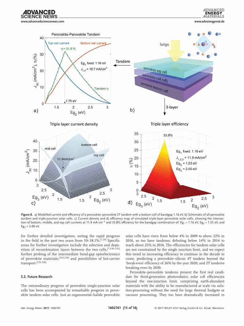
Following the key developments in low bandgap perovs-kites,[2,67,70,127–129] we explore what might be expected of future perovskite tandem solar cells under modest assumptions. We employ a bottom cell of CH3NH3SnxPb(1-x)I3 with bandgap of 1.16 eV[127] to model tandem and triple-layer perovskite solar cells under AM1.5G illumination. We assume 95% transpar-ency for both the top-contact and internal recombination layers, ideal above-bandgap absorption and collection, a loss-in-poten-tial (Eg-qVoc) of 390 mV and fill-factors of 80% from current record cells.[59,85]
Under these simple assumptions we find potential for 2T perovskite tandems beyond 31% efficiency at a matched current of 18.7 mA cm-2 with top cell bandgap of 1.75 eV (Figure 8a), and triple-layer perovskite cells with >33% effi-ciency, with Eg2 = 1.53 eV, Eg3 = 2.00 eV, and a matched cur-rent across the device of 11.9 mA cm-2 (Figure 8c,d). A gain of only ≈2% absolute efficiency is found for a three-layer cell compared to a two-layer cell under these assumptions, limited strongly by the 95% transparency of recombination layers, further underscoring the importance of sub-bandgap transmission for all non-cell layers in tandem architectures. Whilst the real dependence of voltage and current on cell bandgap and architecture is subtler than what we have simu-lated, we present these simple modelling results as incentive
Adv. Energy Mater. 2017, 1602761
www.advenergymat.dewww.advancedsciencenews.com
© 2017 WILEY-VCH Verlag GmbH & Co. KGaA, Weinheim1602761 (15 of 18)
for further detailed investigation, noting the rapid progress in the field in the past two years from 10–18.1%.[7,10] Specific areas for further investigation include the selection and depo-sition of recombination layers between the two cells,[7,130–132] further probing of the intermediate band-gap optoelectronics of perovskite materials,[133,134] and possibilities of hot-carrier transport.[135,136]
5.2. Future Research
The extraordinary progress of perovskite single-junction solar cells has been accompanied by remarkable progress in perov-skite tandem solar cells. Just as organometal–halide perovskite
solar cells have risen from below 4% in 2009 to above 22% in 2016, so too have tandems; debuting below 14% in 2014 to reach above 25% in 2016. The efficiencies for tandem solar cells are not constrained by the single junction limit, and we expect this trend in increasing efficiency to continue in the decade to come, predicting a perovskite–silicon 4T tandem beyond the ‘break-even’ efficiency of 26% by the year 2020, and 2T tandems breaking even by 2030.
Perovskite–perovskite tandems present the first real candi-date for third-generation photovoltaics; solar cell efficiencies beyond the one-junction limit, comprising earth-abundant materials with the ability to be manufactured at scale via solu-tion-processing without the need for large thermal budgets or vacuum processing. They too have dramatically increased in
Adv. Energy Mater. 2017, 1602761
Figure 8. a) Modelled current and efficiency of a perovskite–perovskite 2T tandem with a bottom cell of bandgap 1.16 eV. b) Schematic of all-perovskite tandem and triple-junction solar cells. c) Current density and d) efficiency map of simulated triple-layer perovskite solar cells, showing the intersec-tion of bottom, middle, and top cell currents at 11.9 mA cm-2 and 33.8% efficiency for the bandgap combination of: Eg1 = 1.16 eV, Eg2 = 1.53 eV, and Eg3 = 2.00 eV.

www.advenergymat.dewww.advancedsciencenews.com
© 2017 WILEY-VCH Verlag GmbH & Co. KGaA, Weinheim1602761 (16 of 18)Adv. Energy Mater. 2017, 1602761
efficiency, doubling in their first year with perovskite–perovskite 2T tandems now at 18.1% efficiency and 4T efficiency at 20.3%.[7,8] Further improvements in low-bandgap perovs-kite materials, recombination layers, and contacts will see efficiencies continue to improve. We expect perovskite– perovskite tandems to surpass record perovskite single-junc-tion efficiencies before 2020, with efficiencies greater than 26% expected before 2030. Simple modelling under modest assumptions suggests 2T tandem efficiencies above 30% are eminently achievable.
Whilst laboratory cell efficiency records are expected to con-tinue to tumble, it is hard to see significant market potential for solar cells containing perovskite materials before 2030 without significant advances in stability and development of alternative hole-conductor materials. Perovskite/silicon tandems will have to meet the performance guarantee of silicon panels of 80% performance after 25 years. These lifetime constraints could perhaps be reduced for niche markets (such as flexible devices), for which a device shelf time of 5 to 10 years might suffice, but large scale deployment of GW-scale perovskite photovoltaics will not occur before robust demonstration of stability in envi-ronmental testing.
Alongside the issues of material composition and stability that are common to perovskite single junction solar cells, we identify the following key areas of future investigation for perovskite tandem solar cells:
Reduction of Voc loss-in-potential for high-bandgap perovskites.
Efficient perovskite semiconductors with low bandgap <1.1 eV Fabrication-compatible transparent conductors and recombi-
nation layers without indium Graphene-based transparent contacts overlayed with metal
grids. Wavelength-selective light-trapping techniques with excellent
long-pass transmission. Perovskite compounds that can serve as selective-transport,
transparent contact, and recombination layers in integrated multijunction perovskite devices.
Perovskite materials are the most exciting development to occur in photovoltaic research in the past 20 years. As they tran-sition from the laboratory bench to commercial application, we see clear development pathways toward a future of truly third generation photovoltaics—solar cell efficiencies beyond the one-junction limit, comprising earth-abundant materials man-ufactured at scale, enabling the continuation of Swanson’s Law for decades to come.
AcknowledgementsThis work was financially supported by the Australian Government through the Australian Renewable Energy Agency and the Australian Centre for Advanced Photovoltaics. The authors also acknowledge support from the Australian Research Council (projects CE170100026 and DP160104575) and CSIRO through a OCE Science Leader Fellowship.
Keywordsoptics, perovskites, photovoltaics, tandem, thin films
Received: December 12, 2016Revised: February 18, 2017
Published online:
[1] M. A. Green, A. Ho-Baillie, H. J. Snaith, Nat. Photonics 2014, 8, 506.[2] H. J. Snaith, J. Phys. Chem. Lett. 2013, 4, 3623.[3] National Renewable Energy Laboratory (NREL) PV Efficiency
Chart, http://www.nrel.gov/pv/assets/images/efficiency_chart.jpg (accessed: September, 2016).
[4] P. Loper, S. J. Moon, S. Martin de Nicolas, B. Niesen, M. Ledinsky, S. Nicolay, J. Bailat, J. H. Yum, S. De Wolf, C. Ballif, Phys. Chem. Chem. Phys. 2015, 17, 1619.
[5] J. Werner, L. Barraud, A. Walter, M. Bräuninger, F. Sahli, D. Sacchetto, N. Tétreault, B. Paviet-Salomon, S. J. Moon, C. Allebé, M. Despeisse, S. Nicolay, S. De Wolf, B. Niesen, C. Ballif, ACS Energy Lett. 2016, 1, 474.
[6] M. A. Green, K. Emery, Y. Hishikawa, W. Warta, E. D. Dunlop, D. H. Levi, A. W. Y. Ho-Baillie, Prog. Photovoltaics Res. Appl. 2016, DOI: 10.1002/pip.2855.
[7] G. E. Eperon, T. Leijtens, K. A. Bush, R. Prasanna, T. Green, J. T.-W. Wang, D. P. McMeekin, G. Volonakis, R. L. Milot, R. May, A. Palmstrom, D. J. Slotcavage, R. A. Belisle, J. B. Patel, E. S. Parrott, R. J. Sutton, W. Ma, F. Moghadam, B. Conings, A. Babayigit, H.-G. Boyen, S. Bent, F. Giustino, L. M. Herz, M. B. Johnston, M. D. McGehee, H. J. Snaith, Science 2016, 354, 6314.
[8] D. Forgács, L. Gil-Escrig, D. Pérez-Del-Rey, C. Momblona, J. Werner, B. Niesen, C. Ballif, M. Sessolo, H. J. Bolink, Adv. Energy Mater. 2017, 7, 1602121.
[9] R. M. Swanson, Prog. Photovoltaics Res. Appl. 2006, 14, 443.[10] J. H. Heo, S. H. Im, Adv. Mater. 2016, 28, 5121.[11] Z. Yang, A. Rajagopal, C. C. Chueh, S. B. Jo, B. Liu, T. Zhao,
A. K. Y. Jen, Adv. Mater. 2016, DOI: 10.1002/adma.201602696.[12] S. Albrecht, M. Saliba, P. Correa, F. Lang, L. Korte, R. Schlatmann,
M. K. Nazeeruddin, A. Hagfeldt, M. Grätzel, Energy Environ. Sci. 2015, 9, 81.
[13] J. Werner, C. H. Weng, A. Walter, L. Fesquet, J. P. Seif, S. De Wolf, B. Niesen, C. Ballif, J. Phys. Chem. Lett. 2015, 7.
[14] J. P. Mailoa, C. D. Bailie, E. C. Johlin, E. T. Hoke, A. J. Akey, W. H. Nguyen, M. D. McGehee, T. Buonassisi, Appl. Phys. Lett. 2015, 106, 121105.
[15] C. D. Bailie, M. G. Christoforo, J. P. Mailoa, A. R. Bowring, E. L. Unger, W. H. Nguyen, J. Burschka, N. Pellet, J. Z. Lee, M. Grätzel, R. Noufi, T. Buonassisi, A. Salleo, M. D. McGehee, Energy Environ. Sci. 2015, 8, 956.
[16] B. Chen, Y. Bai, Z. Yu, T. Li, X. Zheng, Q. Dong, L. Shen, M. Boccard, A. Gruverman, Z. Holman, J. Huang, Adv. Energy Mater. 2016. 6, 1601128.
[17] T. Todorov, T. Gershon, O. Gunawan, Y. S. Lee, C. Sturdevant, L. Y. Chang, S. Guha, Adv. Energy Mater. 2015, 5, 1500799.
[18] L. Kranz, A. Abate, T. Feurer, F. Fu, E. Avancini, J. Löckinger, P. Reinhard, S. M. Zakeeruddin, M. Grätzel, S. Buecheler, A. N. Tiwari, J. Phys. Chem. Lett. 2015, 6, 2676.
[19] F. Fu, T. Feurer, T. Jager, E. Avancini, B. Bissig, S. Yoon, S. Buecheler, A. N. Tiwari, Nat. Commun. 2015, 6, 8932.
[20] F. Fu, T. Feurer, T. P. Weiss, S. Pisoni, E. Avancini, C. Andres, S. Buecheler, A. N. Tiwari, Nat. Energy 2016, 2, 16190.
www.advenergymat.dewww.advancedsciencenews.com
© 2017 WILEY-VCH Verlag GmbH & Co. KGaA, Weinheim1602761 (17 of 18)Adv. Energy Mater. 2017, 1602761
[21] T. Todorov, T. Gershon, O. Gunawan, C. Sturdevant, S. Guha, Appl. Phys. Lett. 2014, 105, 173902.
[22] C. C. Chen, S. H. Bae, W.-H. Chang, Z. Hong, G. Li, Q. Chen, H. Zhou, Y. Yang, Mater. Horiz. 2015, 2, 203.
[23] Y. Liu, L. A. Renna, M. Bag, Z. A. Page, P. Kim, J. Choi, T. Emrick, D. Venkataraman, T. P. Russell, ACS Appl. Mater. Interfaces 2016, 8, 7070.
[24] P. Gao, M. Grätzel, M. K. Nazeeruddin, Energy Environ. Sci. 2014, 7, 2448.
[25] P. Docampo, T. Bein, Acc. Chem. Res. 2016, 49, 339.[26] D. Zhao, W. Ke, C. R. Grice, A. J. Cimaroli, X. Tan, M. Yang,
R. W. Collins, H. Zhang, K. Zhu, Y. Yan, Nano Energy 2016, 19, 88.[27] Q. Lin, A. Armin, P. L. Burn, P. Meredith, Acc. Chem. Res. 2016, 49,
545.[28] L. Yang, A. T. Barrows, D. G. Lidzey, T. Wang, Reports Prog. Phys.
2016, 79, 26501.[29] C. D. Bailie, M. D. McGehee, MRS Bull. 2015, 40, 681.[30] T. Todorov, O. Gunawan, S. Guha, Mol. Syst. Des. Eng. 2016,
DOI: 10.1039/C6ME00041J.[31] A. J. Sangster, Green Energy Technol. 2014, 194, 145.[32] PvXchange, http://www.pvxchange.com (accessed: September,
2016).[33] C. Battaglia, A. Cuevas, S. De Wolf, Energy Environ. Sci. 2016, 9,
1552.[34] M. A. Green, Nat. Energy 2016, 1, 15015.[35] S. V Boriskina, M. A. Green, K. Catchpole, E. Yablonovitch,
M. C. Beard, Y. Okada, S. Lany, T. Gershon, A. Zakutayev, M. H. Tahersima, V. J. Sorger, M. J. Naughton, K. Kempa, M. Dagenais, Y. Yao, L. Xu, X. Sheng, N. D. Bronstein, J. A. Rogers, A. P. Alivisatos, R. G. Nuzzo, J. M. Gordon, D. M. Wu, M. D. Wisser, A. Salleo, J. Dionne, P. Bermel, J. J. Greffet, I. Celanovic, M. Soljacic, A. Manor, C. Rotschild, A. Raman, L. Zhu, S. Fan, G. Chen, J. Opt. 2016, 18, 73004.
[36] N. N. Lal, T. P. White, K. R. Catchpole, IEEE J. Photovoltaics 2014, 4, 1380.
[37] J. P. Mailoa, C. D. Bailie, E. C. Johlin, E. T. Hoke, A. J. Akey, W. H. Nguyen, M. D. McGehee, T. Buonassisi, Appl. Phys. Lett. 2015, 106, 121105.
[38] P. Loper, B. Niesen, S. J. Moon, S. Martin de Nicolas, J. Holovsky, Z. Remes, M. Ledinsky, F. J. Haug, J. H. Yum, S. De Wolf, C. Ballif, IEEE J. Photovoltaics 2014, 4, 1545.
[39] M. A. Green, Third Generation Photovoltaics: Advanced Solar Energy Conversion, Springer, Berlin, 2003.
[40] IRENA, Renewable Energy Technologies Cost Analysis 2012, 1, 52.[41] N. G. Park, M. Grätzel, T. Miyasaka, K. Zhu, K. Emery, Nat. Energy
2016, 1, 16152.[42] J. A. Christians, J. S. Manser, P. V Kamat, J. Phys. Chem. Lett. 2015,
6, 852.[43] M. Stocks, Y. X. Loo, N. N. Lal, in 32nd European Photovoltaic Solar
Energy Conference and Exhibition, EU PVCSEC Proceedings 2016, 223.
[44] M. H. Futscher, B. Ehrler, ACS Energy Lett. 2016, 1, 863.[45] S. P. Bremner, M. Y. Levy, C. B. Honsberg, Prog. Photovoltaics Res.
Appl. 2008, 16, 225.[46] A. S. Brown, M. A. Green, Phys. E (Amsterdam, Neth.) 2002, 14, 96.[47] W. Shockley, H. J. Queisser, J. Appl. Phys. 1961, 32, 510.[48] Photovoltaic Education Network, http://PVeducation.org
(accessed: September, 2016).[49] S. R. Kurtz, P. Faine, J. M. Olson, J. Appl. Phys. 1990, 68, 1890.[50] The Hong Kong Polytechnic University, Media Releases, https://
www.polyu.edu.hk/web/en/media/media_releases/index_id_6208.html (accessed: September, 2016).
[51] J. Peng, T. Duong, X. Zhou, H. Shen, Y. Wu, H. K. Mulmudi, Y. Wan, D. Zhong, J. Li, T. Tsuzuki, K. J. Weber, K. R. Catchpole, T. P. White, Adv. Energy Mater. 2016, 6, 1601768.
[52] Y. Zhao, K. Zhu, Chem. Soc. Rev. 2016, 45, 655.[53] S. S. Li, C. H. Chang, Y. C. Wang, C. W. Lin, D. Y. Wang,
J. C. Lin, C. C. Chen, H. S. Sheu, H. C. Chia, W. R. Wu, U. S. Jeng, C. T. Liang, R. Sankar, F. C. Chou, C. W. Chen, Energy Environ. Sci. 2016, 9, 1282.
[54] J. Berry, T. Buonassisi, D. A. Egger, G. Hodes, L. Kronik, Y.-L. Loo, I. Lubomirsky, S. R. Marder, Y. Mastai, J. S. Miller, D. B. Mitzi, Y. Paz, A. M. Rappe, I. Riess, B. Rybtchinski, O. Stafsudd, V. Stevanovic, M. F. Toney, D. Zitoun, A. Kahn, D. Ginley, D. Cahen, Adv. Mater. 2015, 27, 5102.
[55] P. Docampo, T. Bein, Acc. Chem. Res. 2016, 49, 339.[56] K. D. Karlin, D. B. Mitzi, Prog. Inorg. Chem. 2007, 48, 1.[57] B. Saparov, D. B. Mitzi, Chem. Rev. 2016, 116, 4558.[58] G. E. Eperon, S. D. Stranks, C. Menelaou, M. B. Johnston,
L. M. Herz, H. J. Snaith, Energy Environ. Sci. 2014, 7, 982.[59] M. Saliba, T. Matsui, K. Domanski, J. Y. Seo, A. Ummadisingu,
S. M. Zakeeruddin, J. P. Correa-Baena, W. R. Tress, A. Abate, A. Hagfeldt, M. Grätzel, Science 2016, 354, 206.
[60] M. A. Riza, M. A. Ibrahim, U. C. Ahamefula, M. A. Mat Teridi, N. Ahmad Ludin, S. Sepeai, K. Sopian, Sol. Energy 2016, 137, 371.
[61] I. Borriello, G. Cantele, D. Ninno, Phys. Rev. B 2008, 77, 1.[62] F. C. Hanusch, E. Wiesenmayer, E. Mankel, A. Binek, P. Angloher,
C. Fraunhofer, N. Giesbrecht, J. M. Feckl, W. Jaegermann, D. Johrendt, T. Bein, P. Docampo, J. Phys. Chem. Lett. 2014, 5, 2791.
[63] J. T. Jacobsson, J. P. Correa Baena, M. Pazoki, M. Saliba, K. Schenk, M. Grätzel, A. Hagfeldt, Energy Environ. Sci. 2016, 41, 1.
[64] J. L. Knutson, J. D. Martin, D. B. Mitzi, Inorg. Chem. 2005, 44, 4699.
[65] P. Qin, A. L. Domanski, A. K. Chandiran, R. Berger, H.-J. Butt, M. I. Dar, T. Moehl, N. Tetreault, P. Gao, S. Ahmad, M. K. Nazeeruddin, M. Gratzel, Nanoscale 2014, 6, 1508.
[66] N. K. Noel, S. D. Stranks, A. Abate, C. Wehrenfennig, S. Guarnera, A. A. Haghighirad, A. Sadhanala, G. E. Eperon, S. K. Pathak, M. B. Johnston, A. Petrozza, L. M. Herz, H. J. Snaith, Energy Environ. Sci. 2014, 7, 3061.
[67] R. J. Sutton, G. E. Eperon, L. Miranda, E. S. Parrott, B. A. Kamino, J. B. Patel, M. T. Hörantner, M. B. Johnston, A. A. Haghighirad, D. T. Moore, H. J. Snaith, Adv. Energy Mater. 2016, 6, 1502458.
[68] G. Volonakis, M. R. Filip, A. A. Haghighirad, N. Sakai, B. Wenger, H. J. Snaith, F. Giustino, J. Phys. Chem. Lett. 2016, 7, 1254.
[69] E. T. Hoke, D. J. Slotcavage, E. R. Dohner, A. R. Bowring, H. I. Karunadasa, M. D. McGehee, Chem. Sci. 2015, 6, 613.
[70] D. P. McMeekin, G. Sadoughi, W. Rehman, G. E. Eperon, M. Saliba, M. T. Hörantner, A. Haghighirad, N. Sakai, L. Korte, B. Rech, M. B. Johnston, L. M. Herz, H. J. Snaith, Science 2016, 351, 151.
[71] J. W. Lee, D. H. Kim, H. S. Kim, S. W. Seo, S. M. Cho, N. G. Park, Adv. Energy Mater. 2015, 5, 1501310.
[72] Q. Ma, S. Huang, X. Wen, M. A. Green, A. W. Y. Ho-Baillie, Adv. Energy Mater. 2016, 6, 1502202.
[73] M. R. Filip, G. E. Eperon, H. J. Snaith, F. Giustino, Nat. Commun. 2014, 5, 5757.
[74] E. Mosconi, A. Amat, M. K. Nazeeruddin, M. Grätzel, F. De Angelis, J. Phys. Chem. C 2013, 117, 13902.
[75] J. Im, C. C. Stoumpos, H. Jin, A. J. Freeman, M. G. Kanatzidis, J. Phys. Chem. Lett. 2015, 6, 3503.
[76] N. K. Noel, S. D. Stranks, A. Abate, C. Wehrenfennig, S. Guarnera, A.-A. Haghighirad, A. Sadhanala, G. E. Eperon, S. K. Pathak, M. B. Johnston, A. Petrozza, L. M. Herz, H. J. Snaith, Energy Environ. Sci. 2014, 7, 3061.
[77] M. G. Kanatzidis, F. Hao, C. C. Stoumpos, D. H. Cao, R. P. H. Chang, Nat. Photonics 2014, 8, 489.
[78] F. Hao, C. C. Stoumpos, D. H. Cao, R. P. H. Chang, M. G. Kanatzidis, Nat. Photonics 2014, 8, 489.

www.advenergymat.dewww.advancedsciencenews.com
© 2017 WILEY-VCH Verlag GmbH & Co. KGaA, Weinheim1602761 (18 of 18)Adv. Energy Mater. 2017, 1602761
[79] S. De Wolf, J. Holovsky, S. J. Moon, P. Löper, B. Niesen, M. Ledinsky, F.-J. Haug, J.-H. Yum, C. Ballif, J. Phys. Chem. Lett. 2014, 5, 1035.
[80] M. Filipic, P. Löper, B. Niesen, S. De Wolf, J. Krc, C. Ballif, M. Topic , Opt. Express 2015, 23, A263.
[81] Q. Jiang, L. Zhang, H. Wang, X. Yang, J. Meng, H. Liu, Z. Yin, J. Wu, X. Zhang, J. You, Nat. Energy 2016, 2, 16177.
[82] V. Ganapati, M. A. Steiner, E. Yablonovitch, IEEE J. Photovoltaics 2016, 6, 801.
[83] E. Yablonovitch, O. D. Miller, S. R. Kurtz, in 2012 38th IEEE Photo-volt. Spec. Conf., IEEE, 2012, 1556.
[84] F. Deschler, M. Price, S. Pathak, L. Klintberg, D. D. Jarausch, R. Higler, S. Huettner, T. Leijtens, S. D. Stranks, H. J. Snaith, M. Atature, R. T. Phillips, R. H. Friend, J. Phys. Chem. Lett. 2014, 5, 1421.
[85] M. A. Green, K. Emery, Y. Hishikawa, W. Warta, E. D. Dunlop, Prog. Photovolt: Res. Appl. 2016, 24, 905.
[86] R. T. Ross, J. Chem. Phys. 1967, 46, 4590.[87] W. S. Yang, J. H. Noh, N. J. Jeon, Y. C. Kim, S. Ryu, J. Seo,
S. Il Seok, Science. 2015, 348, 1234.[88] R. Sheng, A. Ho-Baillie, S. Huang, S. Chen, X. Wen, X. Hao,
M. A. Green, J. Phys. Chem. 2015, 119, 3545.[89] D. W. de Quilettes, S. M. Vorpahl, S. D. Stranks, H. Nagaoka,
G. E. Eperon, M. E. Ziffer, H. J. Snaith, D. S. Ginger, Science 2015, 348, 6235.
[90] J. P. Correa Baena, L. Steier, W. Tress, M. Saliba, S. Neutzner, T. Matsui, F. Giordano, T. J. Jacobsson, A. R. Srimath Kandada, S. M. Zakeeruddin, A. Petrozza, A. Abate, M. K. Nazeeruddin, M. Gratzel, A. Hagfeldt, Energy Environ. Sci. 2015, 8, 2928.
[91] G. Niu, X. Guo, L. Wang, J. Mater. Chem. A 2015, 3, 8970.[92] J. Zhao, X. Zheng, Y. Deng, T. Li, Y. Shao, A. Gruverman, J. Shield,
J. Huang, Energy Environ. Sci. 2016, 8, 1953.[93] J. H. Noh, S. H. Im, J. H. Heo, T. N. Mandal, S. Il Seok, Nano Lett.
2013, 13, 1764.[94] Y. Yuan, J. Huang, Acc. Chem. Res. 2016, 49, 286.[95] E. M. Sanehira, B. J. Tremolet de Villers, P. Schulz, M. O. Reese,
S. Ferrere, K. Zhu, L. Y. Lin, J. J. Berry, J. M. Luther, ACS Energy Lett. 2016, 1, 38.
[96] R. E. Beal, D. J. Slotcavage, T. Leijtens, A. R. Bowring, R. A. Belisle, W. H. Nguyen, G. F. Burkhard, E. T. Hoke, M. D. McGehee, J. Phys. Chem. Lett. 2016, 7, 746.
[97] J. H. Heo, H. J. Han, D. Kim, T. K. Ahn, S. H. Im, Energy Environ. Sci. 2015, 8, 1602.
[98] K. A. Bush, C. D. Bailie, Y. Chen, A. R. Bowring, W. Wang, W. Ma, T. Leijtens, F. Moghadam, M. D. McGehee, Adv. Mater. 2016, 28, 3937.
[99] X. Y. Zeng, Q. K. Zhang, R. M. Yu, C. Z. Lu, Adv. Mater. 2010, 22, 4484.
[100] S. Albrecht, M. Saliba, J. P. Correa-Baena, K. Jäger, L. Korte, A. Hagfeldt, M. Grätzel, B. Rech, J. Opt. 2016, 18, 64012.
[101] G. Conibeer, M. A. Green, R. Corkish, Y. Cho, E. C. Cho, C. W. Jiang, T. Fangsuwannarak, E. Pink, Y. Huang, T. Puzzer, T. Trupke, B. Richards, A. Shalav, K. Lin, Thin Solid Films 2006, 511, 654.
[102] Y. Jiang, I. Almansouri, S. Huang, T. Young, Y. Li, Y. Peng, Q. Hou, L. Spiccia, U. Bach, Y. B. Cheng, M. Green, A. Ho-Baillie, J. Mater. Chem. C 2016, 4, 5679.
[103] D. A. Jacobs, K. R. Catchpole, F. J. Beck, T. P. White, J. Mater. Chem. A 2016, 4, 4490.
[104] T. Duong, N. Lal, D. Grant, D. Jacobs, P. Zheng, S. Rahman, H. Shen, M. Stocks, A. Blakers, K. Weber, T. P. White, K. R. Catchpole, IEEE J. Photovoltaics 2016, 6, 679.
[105] F. Lang, M. A. Gluba, S. Albrecht, J. Rappich, L. Korte, B. Rech, N. H. Nickel, J. Phys. Chem. Lett. 2015, 2745.
[106] J. Werner, G. Dubuis, A. Walter, P. Löper, S.-J. Moon, S. Nicolay, M. Morales-Masis, S. De Wolf, B. Niesen, C. Ballif, Sol. Energy Mater. Sol. Cells 2015, 141, 407.
[107] K. Ellmer, Nat. Photonics 2012, 6, 809.[108] R. A. Powell, S. Rossnagel, PVD for Microelectronics: Sputter
Deposition Applied to Semiconductor Manufacturing, Academic Press, San Diego, 1998.
[109] J. George, C. S. Menon, Surf. Coatings Technol. 2000, 132, 45.[110] T. Koida, H. Sai, M. Kondo, Thin Solid Films 2010, 518, 2930.[111] T. Koida, H. Fujiwara, Sol. Energy Mater. Sol. Cells 2009, 93, 851.[112] E. Nakamura, K. Sato, Nat. Mater. 2011, 10, 158.[113] D. Cheyns, B. Kam, K. Vasseur, P. Heremans, B. P. Rand, J. Appl.
Phys. 2013, 113, 43109.[114] J. Werner, J. Geissbühler, A. Dabirian, S. Nicolay,
M. Morales-Masis, S. De Wolf, B. Niesen, C. Ballif, ACS Appl. Mater. Interfaces 2016, 8, 17260.
[115] X. Liu, C. C. Chueh, Z. Zhu, S. B. Jo, Y. Sun, A. K. Y. Jen, J. Mater. Chem. A. 2016, 4, 15294.
[116] D. T. Grant, K. R. Catchpole, K. J. Weber, T. P. White, Opt. Express 2016, 24, A1454.
[117] M. Filipic , P. Löper, B. Niesen, S. De Wolf, J. Krc , C. Ballif, M. Topic , Opt. Express 2015, 23, A263.
[118] M. Grätzel, Nat. Mater. 2014, 13, 838.[119] U. Bach, Nat. Chem. 2015, 7, 616.[120] V. Zardetto, B. L. Williams, A. Perrotta, F. Di Giacorno,
M. A. Verheijen, R. Andriessen, W. M. M. Kessels, M. Creatore, Sustainable Energy and Fuels 2017, DOI: 10.1039/C6SE00076B.
[121] K. Wojciechowski, T. Leijtens, S. Siprova, C. Schlueter, M. T. Hörantner, J. T.-W. Wang, C.-Z. Li, A. K. Y. Jen, T.-L. Lee, H. J. Snaith, J. Phys. Chem. Lett. 2015, 6, 2399.
[122] J. H. Kim, C.-C. Chueh, S. T. Williams, A. K.-Y. Jen, Nanoscale 2015, 7, 17343.
[123] F. Guo, H. Azimi, Y. Hou, T. Przybilla, M. Hu, C. Bronnbauer, S. Langner, E. Spiecker, K. Forberich, C. J. Brabec, Nanoscale 2015, 7, 1642.
[124] F. Lang, M. A. Gluba, S. Albrecht, J. Rappich, L. Korte, B. Rech, N. H. Nickel, J. Phys. Chem. Lett. 2015, 2745.
[125] W. Li, G. Cheng, Y. Liang, B. Tian, X. Liang, L. Peng, A. R. Hight Walker, D. J. Gundlach, N. V Nguyen, Carbon 2016, 99, 348.
[126] X. Li, W. Cai, J. An, S. Kim, J. Nah, D. Yang, R. Piner, A. Velamakanni, I. Jung, E. Tutuc, S. K. Banerjee, L. Colombo, R. S. Ruoff, Science 2009, 324, 1312.
[127] Y. Ogomi, A. Morita, S. Tsukamoto, T. Saitho, N. Fujikawa, Q. Shen, T. Toyoda, K. Yoshino, S. S. Pandey, T. Ma, S. Hayase, J. Phys. Chem. Lett. 2014, 5, 1004.
[128] Q. Shen, Y. Ogomi, J. Chang, T. Toyoda, K. Fujiwara, K. Yoshino, K. Sato, K. Yamazaki, M. Akimoto, Y. Kuga, K. Katayama, S. Hayase, J. Mater. Chem. A 2015, 3, 9308.
[129] G. E. Eperon, G. M. Paterno, R. J. Sutton, A. Zampetti, A. A. Haghighirad, F. Cacialli, H. J. Snaith, J. Mater. Chem. A 2015, 3, 19688.
[130] J. You, L. Dou, Z. Hong, G. Li, Y. Yang, Prog. Polym. Sci. 2013, 38, 1909.
[131] V. C. Tung, J. Kim, L. J. Cote, J. Huang, J. Am. Chem. Soc. 2011, 133, 9262.
[132] F. Jiang, T. Liu, B. Luo, J. Tong, F. Qin, S. Xiong, Z. Li, Y. Zhou, J. Mater. Chem. A 2016, 4, 1208.
[133] A. Luque, A. Marti, Adv. Mater. 2010, 22, 160.[134] A. Luque, A. Martí, C. Stanley, Nat. Photonics 2012, 6, 146.[135] M. B. Price, J. Butkus, T. C. Jellicoe, A. Sadhanala, A. Briane,
J. E. Halpert, K. Broch, J. M. Hodgkiss, R. H. Friend, F. Deschler, Nat. Commun. 2015, 6, 8420.
[136] M. A. Green, S. P. Bremner, Nat. Mater. 2017, 16, 23.


![[Enter your title here] - CreativeCreation - ronn andriessen.pdfTriple cation perovskite for tandem with c-Si cells Absolute efficiency increase of 2.4% compared to standalone c-Si](https://static.fdocuments.in/doc/165x107/60a80cae323c8f08c34d393b/enter-your-title-here-ronn-andriessenpdf-triple-cation-perovskite-for-tandem.jpg)