Performance Specification KAF-1001E - Uppsala University · 2013-08-01 · Performance...
18
KAF-1001E Performance Specification KAF - 1001E 1024(H) x 1024(V) Pixel Enhanced Response Full-Frame CCD Image Sensor Performance Specification Eastman Kodak Company Image Sensor Solutions Rochester, New York 14650 Revision 2.0 March 19, 2004 Eastman Kodak Company - Image Sensor Solutions For the most current information regarding this product: Phone: (585) 722-4385 Fax: (585) 477-4947 Web: www.kodak.com/go/imagers E-mail: [email protected]
Transcript of Performance Specification KAF-1001E - Uppsala University · 2013-08-01 · Performance...

KAF-1001EPerformance Specification
KAF - 1001E
1024(H) x 1024(V) Pixel
Enhanced Response
Full-Frame CCD Image Sensor
Performance Specification
Eastman Kodak Company
Image Sensor Solutions
Rochester, New York 14650
Revision 2.0 March 19, 2004
Eastman Kodak Company - Image Sensor SolutionsFor the most current information regarding this product:
Phone: (585) 722-4385 Fax: (585) 477-4947 Web: www.kodak.com/go/imagers E-mail: [email protected]
KAF-1001EPerformance Specification
TABLE OF CONTENTS
1.1 Features ............................................................................................................................................3 1.2 Description.......................................................................................................................................3 1.3 Architecture .....................................................................................................................................4 1.4 Image Acquisition............................................................................................................................4 1.5 Charge Transport .............................................................................................................................4 1.6 Output Structure...............................................................................................................................4 2.1 Package Configuration.....................................................................................................................5 2.2 Pin Description ................................................................................................................................6 3.1 Absolute Maximum Ratings ............................................................................................................8 3.2 DC Operating Conditions ................................................................................................................8 3.3 AC Clock Level Conditions.............................................................................................................9 3.4 AC Timing .....................................................................................................................................10 4.1 Image Specifications......................................................................................................................12 4.2 Defect Classification......................................................................................................................14 4.3 Typical Performance Data .............................................................................................................15 5.1 Quality Assurance and Reliability .................................................................................................17 5.2 Ordering Information .....................................................................................................................17 6.1 Revision Changes ..........................................................................................................................18
FIGURES
Figure 1 Functional Block Diagram ......................................................................................................3 Figure 2 Package Configuration ............................................................................................................5 Figure 3 Pinout Diagram........................................................................................................................7 Figure 4 Timing Diagram ....................................................................................................................12 Figure 5 Typical Spectral Response ....................................................................................................15 Figure 6 Dark Current as a Function of Temperature..........................................................................16
Eastman Kodak Company - Image Sensor SolutionsFor the most current information regarding this product:
Phone: (585) 722-4385 Fax: (585) 477-4947 Web: www.kodak.com/go/imagers E-mail: [email protected] 2 Revision No. 2.0

KAF-1001EPerformance Specification
1.1 Features • Front Illuminated Full-Frame Architecture
with Blue Plus Transparent Gate True Two Phase Technology for high sensitivity
• 1024(H) x 1024(V) Photosensitive Pixels • 24µm(H) x 24µm(V) Pixel Size • 24.5 mm x 24.5 mm Photo active Area • 1:1 Aspect Ratio • 100% Fill Factor • Single Readout Register • 2 Clock Selectable Outputs • High Gain Output (11 µV/e-) for low noise • Low Gain Output (2.0 µV/e-) for high
dynamic range • Low Dark Current (<30 pA/cm2 @ T=25oC)
1.2 Description The KAF-1001E is a high-performance, silicon charge-coupled device (CCD) designed for a wide range of image sensing applications in the 0.4mm to 1.1mm wavelength band.
Common applications include medical, scientific, military, machine and industrial vision. The sensor is built with a true two-phase CCD technology employing a transparent gate. This technology simplifies the support circuits that drive the sensor and reduces the dark current without compromising charge capacity. The transparent gate results in spectral response increased ten times at 400nm, compared to a front side illuminated standard polysilicon gate technology. The sensitivity is increased 50% over the rest of the visible wavelengths. The clock selectable on-chip output amplifiers have been specially designed to meet two different needs. The first is a high sensitivity 2-stage output with 11µV/e- charge to voltage conversion ratio. The second is a single-stage output with 2µV/e- charge to voltage conversion ratio.
KAF-1001E
Usable Active Image Area1024(H) x 1024(V)
24µm x 24µm pixels
4 Dark Lines
φV1
φV2
Guard
4 Dark Lines
1024 Active Pixels/Line8 Dark2 Inactive
4 Dark4 Inactive
φH22
φH21
φR
VogVrd
Vout 1Vdd 1
VssVout 2Vdd 2Sub
FD 1 FD 2
φH1φH2
Figure 1 - Functional Block Diagram
(Shaded areas represent 4 non-imaging pixels at the beginning and 8 non-imaging pixels at the end of each line. There are also 4 non-imaging lines at the top and bottom of each frame.)
Eastman Kodak Company - Image Sensor SolutionsFor the most current information regarding this product:
Phone: (585) 722-4385 Fax: (585) 477-4947 Web: www.kodak.com/go/imagers E-mail: [email protected] 3 Revision No. 2.0

KAF-1001EPerformance Specification
1.3 Architecture Refer to the block diagram in Figure 1. The KAF-1001E consists of one vertical (parallel) CCD shift register, one horizontal (serial) CCD shift register and a selectable high or low gain output amplifier. Both registers incorporate true two-phase buried channel technology. The vertical register consists of 24µm x 24µm photo-capacitor sensing elements (pixels) which also serves as the transport mechanism. The pixels are arranged in a 1024(H) x 1024(V) array; an additional 12 columns (4 at the left and 8 at the right) and 8 rows (4 each at top and bottom) of non-imaging pixels are added as dark reference. Because there is no storage array, this device must be synchronized with strobe illumination or shuttered during readout.
1.4 Image Acquisition An image is acquired when incident light, in the form of photons, falls on the array of pixels in the vertical CCD register and creates electron-hole pairs (or simply electrons) within the silicon substrate. This charge is collected locally by the formation of potential wells created at each pixel site by induced voltages on the vertical register clock lines (φV1, φV2). These same clock lines are used to implement the transport mechanism as well. The amount of charge collected at each pixel is linearly dependent on light level and exposure time and non-linearly dependent on wavelength until the potential well capacity is exceeded. At this point charge will 'bloom' into vertically adjacent pixels.
1.5 Charge Transport Integrated charge is transported to the output in a two step process. Rows of charge are first shifted line by line into the horizontal CCD. 'Lines' of charge are then shifted to the output pixel by pixel. Referring to the timing diagram, integration of charge is performed with φV1 and φV2 held low. Transfer to horizontal CCD begins when φV1 is brought high causing charge from the φV1 and φV2 gates to combine under the φV1 gate.
φV1 and φV2 now reverse their polarity causing the charge packets to 'spill' forward under the φV2 gate of the next pixel. The rising edge of φV2 also transfers the first line of charge into the horizontal CCD. A second phase transition places the charge packets under the φV1 electrode of the next pixel. The sequence completes when φV1 is brought low. Clocking of the vertical register in this way is known as accumulation mode clocking. Next, the horizontal CCD reads out the first line of charge using traditional complementary clocking (using φH1 and φH2 pins) as shown. The falling edge of φH2 forces a charge packet over the output gate (OG) onto one of the output nodes (floating diffusion) which controls the output amplifier. The cycle repeats until all lines are read.
1.6 Output Structure The final gate of the horizontal register is split into two sections, φH21 and φH22. The split gate structure allows the user to select either of the two output amplifiers. To use the high dynamic range single-stage output (Vout1), tie φH22 to a negative voltage to block charge transfer, and tie φH21 to φH2 to transfer charge. To use the high sensitivity two-stage output (Vout2), tie φH21 to a negative voltage and φH22 to φH2. The charge packets are then dumped onto the appropriate floating diffusion output node whose potential varies linearly with the quantity of charge in each packet. The amount of potential change is determined by the simple expression ∆Vfd=∆Q/Cfd. The translation from electrons to voltages is called the output sensitivity or charge-to-voltage conversion. After the output has been sensed off-chip, the reset clock (φR) removes the charge from the floating diffusion via the reset drain (VRD). This, in turn, returns the floating diffusion potential to the reference level determined by the reset drain voltage.
Eastman Kodak Company - Image Sensor SolutionsFor the most current information regarding this product:
Phone: (585) 722-4385 Fax: (585) 477-4947 Web: www.kodak.com/go/imagers E-mail: [email protected] 4 Revision No. 2.0

KAF-1001EPerformance Specification
2.1 Package Configuration
Figure 2 - Package Drawing
Eastman Kodak Company - Image Sensor SolutionsFor the most current information regarding this product:
Phone: (585) 722-4385 Fax: (585) 477-4947 Web: www.kodak.com/go/imagers E-mail: [email protected] 5 Revision No. 2.0

KAF-1001EPerformance Specification
2.2 Pin Description
Pin Number Symbol Description Notes
1, 4, 26 SUBSTRATE Substrate 2, 21, 25 φV2 Vertical (Parallel) CCD Clock - Phase 2 2 3, 22, 24 φV1 Vertical (Parallel) CCD Clock - Phase 1 1
5 VOUT2 Video Output from High Sensitivity Two-Stage Amplifier 6 VDD2 High Sensitivity Two-Stage Amplifier Supply 7 VLG First Stage Load Transistor Gate for Two-Stage Amplifier 8 VSS Output Amplifier Return 9 φR Reset Clock
10 VRD Reset Drain 11 VDD1 High Dynamic Range Single-Stage Amplifier Supply 12 VOUT1 Video Output from High Dynamic Range Single-Stage 13 OG Output Gate 14 φH21 Last Horizontal (Serial) CCD Phase - Split Gate 15 φH22 Last Horizontal (Serial) CCD Phase - Split Gate 16 φH1 Horizontal (Serial) CCD Clock - Phase 1 17 φH2 Horizontal (Serial) CCD Clock - Phase 2
18, 19, 20 N/C No Connect 23 GUARD Guard Ring
Notes: 1. Pins 3, 22, and 24 must be connected together - only one Phase 1 clock driver is required 2. Pins 2, 21, and 25 must be connected together - only one Phase 2 clock driver is required
Eastman Kodak Company - Image Sensor SolutionsFor the most current information regarding this product:
Phone: (585) 722-4385 Fax: (585) 477-4947 Web: www.kodak.com/go/imagers E-mail: [email protected] 6 Revision No. 2.0

KAF-1001EPerformance Specification
Pixel (1,1)
1
2
3
4
5
6
7
8
9
10
11
12
13G
2
2
VRD
VSS
φR
SUB
φV1
φV2
SUB
VLG
VDD1
OUT1
VO
VOUT
VDD
V
26
25
24
23
22
21
20
19
18
17
16
15
14
φH1
φH2
SUB
N/C
φV1
φV2
φH22
φH21
N/C
N/C
φV2
φV1
GUARD
Pixel (1024,1024)
Figure 3 - Pin Identification Diagram
Eastman Kodak Company - Image Sensor SolutionsFor the most current information regarding this product:
Phone: (585) 722-4385 Fax: (585) 477-4947 Web: www.kodak.com/go/imagers E-mail: [email protected] 7 Revision No. 2.0

KAF-1001EPerformance Specification
3.1 Absolute Minimum/Maximum Ratings
Min. Max. Units Conditions Temperature Storage -100 +80 C At Device
Operating -50 +50 All Clocks -16 +16
Voltage OG 0 +8 V VSUB = OV VRD, VSS, VDD, GUARD 0 +20
Current Output Bias Current (IDD) 10 mA Capacitance Output Load Capacitance (CLOAD) 10 pF
φV1, φV2 Pulse Width 8 µs Frequency/Time φH1, φH2 5 MHz
φR Pulse Width 20 ns
Warning: For maximum performance, built-in gate protection has been added only to the OG pin. These devices require extreme care during handling to prevent electrostatic discharge (ESD) induced damage.
3.2 DC Operating Conditions
Min. Nom. Max. Units Pin Impedance VSUB Substrate 0.0 0.0 0.0 V Common VDD Output Amplifier Supply 15.0 +17.0 17.5 V 5 pf, 2K?
(Note 1) VSS Output Amplifier Return 1.4 +2.0 2.1 V 5 pf, 2K? VRD Reset Drain 11.5 +12 12.5 V 5 pf, 1M? OG Output Gate 3.0 +4.0 4.5 V 5 pf, 10M?
GUARD Guard Ring 7.0 +10.0 15.0 V 350 pF, 10M? VLG Load Gate 0.5 +0.0 1.0 V
Notes: 1. Vdd = 17 volts for applications where the expected output voltage > 2.0 volts. For applications where the expected useable output
voltsge is <2 volts, Vdd can be reduced to 15 volts.
Eastman Kodak Company - Image Sensor SolutionsFor the most current information regarding this product:
Phone: (585) 722-4385 Fax: (585) 477-4947 Web: www.kodak.com/go/imagers E-mail: [email protected] 8 Revision No. 2.0

KAF-1001EPerformance Specification
3.3 AC Clock Level Conditions
Min. Nom. Max. Units Pin Impedance φV1 Vertical Clock -
Phase 1 Low -10.25 -10 -9.8 V 200nF, 10MΩ
High 0.0 0 1.0 V φV2 Vertical Clock -
Phase 2 Low -10.25 -10.0 -9.8 V 200nF, 10MΩ
High 0.0 0 1.0 V CφV1-V2 = 100nF φH1 Horizontal Clock -
Phase 1 Low -2.2 -2.0 -1.8 V 400pF, 10MΩ
High 7.8 +8.0 8.2 V φH2 Horizontal Clock -
Phase 2 Low -2.2 -2.0 -1.8 V 250pF, 10MΩ
High 7.8 +8.0 8.2 V Cφh1-h2 =200pF φR Reset Clock Low 2.0 3.0 3.5 V 10pF, 10MΩ High 9.5 10.0 11.0 V
Using the High Gain
Output (Vout2) Using the High Dynamic Range Output (Vout1)
Min. Nom. Max. Min. Nom Max. Units Pin Impedance
φH21 Horizontal Clock - Phase 1
Low -4 φH2 low
φH2 low
φH2 V 10pF, 10MΩ
High -4 φH2 low
φH2 low
φH2 V
φH22 Horizontal Clock - Phase 2
Low φH2 -4 φH2 low
φH2 low
V 10pF, 10MΩ
High φH2 -4 φH2 low
φH2 low
V
Notes: 1. When using Vout1 φH21 is clocked identically with φH2 while φH22 is held at a static level. When using Vout2 φH21 and φH22
are exchanged so that φH22 is identical to φH2 and φH21 is held at a static level. The static level should be the same voltage as φH2 low.
2. The AC and DC operating levels are for room temperature operation. Operation at other temperatures may require adjustments of these voltages. Pins shown with impedances greater than 1 MOhm are expected resistances. These pins are only verified to 1 MOhm.
3. φV1, 2 capacitances are accumulated gate oxide capacitance, and so are an over-estimate of the capacitance. 4. This device is suitable for a wide range of applications requiring a variety of different operating conditions. Consult Eastman
Kodak in those situations in which operating conditions meet or exceed minimum or maximum levels.
Eastman Kodak Company - Image Sensor SolutionsFor the most current information regarding this product:
Phone: (585) 722-4385 Fax: (585) 477-4947 Web: www.kodak.com/go/imagers E-mail: [email protected] 9 Revision No. 2.0

KAF-1001EPerformance Specification
3.4 AC Timing Chart
Description Symbol Min. Nom. Max. Units Notes φH1, φH2 Clock Frequency fH 4 5 MHz 1, 2, 3 φV1, φV2 Clock Frequency fV 100 125 kHz 1, 2, 3 Pixel Period (1 Count) tpix 200 250 ns φH1, φH2 Setup Time tφHS 500 1000 ns φV1, φV2 Clock Pulse Width tφV 4 5 µs 2 Reset Clock Pulse Width tφR 20 60 ns 4 Readout Time treadout 226 286 ms 5 Integration Time tint 6 Line Time tline 219 277 µs 7
Notes: 1. 50% duty cycle values. 2. CTE may degrade above the nominal frequency. 3. Rise and fall times (10/90% levels) should be limited to 5-10% of clock period. Crossover of register clocks should be between 40-
60% of amplitude. 4. φR should be clocked continuously 5. treadout = (1032 * tline) 6. Integration time (tint) is user specified. Longer integration times will degrade noise performance due to dark signal fixed pattern and
shot noise. 7. tline= (3 * tφV) + tφHS + 1044* tpix + tpix
Eastman Kodak Company - Image Sensor SolutionsFor the most current information regarding this product:
Phone: (585) 722-4385 Fax: (585) 477-4947 Web: www.kodak.com/go/imagers E-mail: [email protected] 10 Revision No. 2.0

KAF-1001EPerformance Specification
AC Timing Diagram
Note: This device is suitable for a wide range of applications requiring a variety of different timing frequencies. Therefore, only
maximum and minimum values are shown above. Consult Eastman Kodak in those situations that require special consideration
tReadouttint
1 Frame = 1032 lines
φH2
φH1
φV1
φV2 Line 1 2 1031 1032
Frame Timing
1044 counts
φH2
φR
φH1
φV1
φV2
1 line
tpixtφHS
Line Timing Detail
tφV
tφV
Line Content
1-4 5-8 9-1032 1033-1042 1043-1044
Dummy Pixels
Photoactive Pixels
Dark Reference Pixels
1 counttpix
tφR
φR
φH1
φH2
VdarkVodc
Vpix
Vsub
Vout
Pixel Timing Detail
Vsat
Vsat Saturated pixel video output signal
Vdark Video output signal in no-light situation, not zero due to Jdark
Vpix Pixel video output signal level; more electrons = more negative
Vodc Video level offset with respect to vsub*
Vsub Analog Ground
* See Image Acquisition section
Figure 4 - Timing Diagram
Eastman Kodak Company - Image Sensor SolutionsFor the most current information regarding this product:
Phone: (585) 722-4385 Fax: (585) 477-4947 Web: www.kodak.com/go/imagers E-mail: [email protected] 11 Revision No. 2.0

KAF-1001EPerformance Specification
4.1 Image Specifications All values derived using nominal operating conditions with the recommended timing. Correlated doubling sampling of the output is assumed and recommended. Many units are expressed in electrons - to convert to voltage, multiply by the amplifier sensitivity. Electro-Optical
Symbol Parameter Min. Nom. Max. Units Condition F F Optical Fill Factor 100 %
PRNU Photoresponse Non-uniformity 5 % rms Full Array QE Quantum Efficiency
(450, 550, 650nm) See QE curve
CCD Parameters Common To both Outputs
Symbol Parameter Min. Nom. Max. Units Condition Ne-sat Sat. Signal - Vccd register 450 500 ke Note 2
Jd Dark Current 15.3 550
30 1080
pA/cm2 e-pixel/sec
25°C (mean of all pixels)
DCDR Dark Current Doubling Temp 5 6 7 oC DSNU Dark Signal Non-uniformity 1080 e-/pix/sec Note 4 CTE Charge Transfer Efficiency .99997 Note 5 tVH V-H CCD Transfer Time 32 µs Notes 6, 7 Bs Blooming Suppression none
CCD Parameters Specific to High Gain Output Amplifier
Symbol Parameter Min. Nom. Max. Units Condition Vout/Ne- Output Sensitivity 9 11 uV/electron
Ne-sat Sat. Signal 180 200 240 ke- Note 1 ne-total Total Sensor Noise 13 20 e- rms Note 8
FH Horizontal CCD Frequency: 2 5 MHz Note 6 DR Dynamic Range : 79 83 dB Note 9
Eastman Kodak Company - Image Sensor SolutionsFor the most current information regarding this product:
Phone: (585) 722-4385 Fax: (585) 477-4947 Web: www.kodak.com/go/imagers E-mail: [email protected] 12 Revision No. 2.0

KAF-1001EPerformance Specification
CCD Parameters Specific to Low Gain (high dynamic range) Output Amplifier
Symbol Parameter Min. Nom. Max. Units Condition Vout/Ne- Output Sensitivity 1.7 2 uV/electron
Ne-sat Sat. Signal 1400 1500 1800 ke- Note 3 ne-total Total Sensor Noise 22 30 e- rms Note 8
FH Horizontal CCD Frequency: 0.5 2 MHz Note 6 DR Dynamic Range : 89 87 dB Note 9
Notes: 1. Point where the output saturates when operated with nominal voltages. 2. Signal level at the onset of blooming in the vertical (parallel) CCD register 3. Maximum signal level at the output of the high dynamic range output. This signal level will only be achieved when binning pixels
containing large signals. 4. None of 64 sub arrays (128 x 128) exceed the maximum dark current specification. 5. For 2MHz data rate and T = 30 C to -40°C. 6. Using maximum CCD frequency and/or minimum CCD transfer times may compromise performance 7. Time between the rising edge of φV1 and the first falling edge of φH1 8. At Tintegration = 0; data rate = 1 MHz; temperature = -30 C 9. Uses 20LOG(Ne- sat / ne- total) where Ne- sat refers to the appropriate saturation signal.
Eastman Kodak Company - Image Sensor SolutionsFor the most current information regarding this product:
Phone: (585) 722-4385 Fax: (585) 477-4947 Web: www.kodak.com/go/imagers E-mail: [email protected] 13 Revision No. 2.0
KAF-1001EPerformance Specification
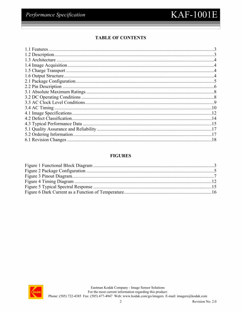
4.2 Cosmetic Grades
Standard: Class Point Defects Cluster Defects Column Defects
C1 20 2 0 C2 40 10 2
Dark Defect A pixel which deviates by more than 20% from neighboring pixels when illuminated to 70% of saturation
Bright Defect A pixel whose dark current exceeds 4500 electrons/pixel/second at 25°C
Cluster Defect A grouping of not more than 5 adjacent point defects.
Column Defect 1) A grouping point defects along a single column. (Dark Column) 2) A column that contains a pixel whose dark current exceeds 150,000
electrons/pixel/second at 25 C. (Bright Column) 3) A column that does not exhibit the minimum charge capacity
specification. (Low charge capacity) 4) A column that loses >500 electrons when the array is illuminated to a
signal level of 2000 electrons/pix. (Trap like defects)
Neighboring Pixels The surrounding 128 x 128 pixels of ± 64 columns/rows Defects are separated by no less than 3 pixels in any one direction.
1,1024 1024,1024
All pixels subject to defect specification
1,1 1024,1
Eastman Kodak Company - Image Sensor SolutionsFor the most current information regarding this product:
Phone: (585) 722-4385 Fax: (585) 477-4947 Web: www.kodak.com/go/imagers E-mail: [email protected] 14 Revision No. 2.0
KAF-1001EPerformance Specification
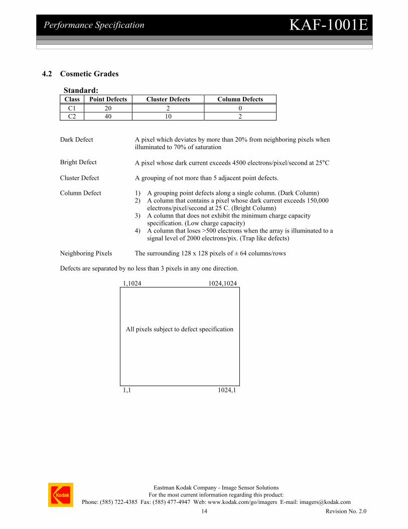
4.3 Typical Performance Data
Kodak Full Frame Image SensorSpectral Response
0
0.1
0.2
0.3
0.4
0.5
0.6
0.7
0.8
0.9
1
300 400 500 600 700 800 900 1000 1100
Wavelength (nm)
Abs
olut
e Q
uant
um E
ffici
ency
KAF-1001E : 24 um pixel KAF-1401E: 6.8 um pixel
Figure 5 - Typical Spectral Response
Figure 5 shows a representative spectral response of front side illuminated transparent gate full frame image sensors. The KAF-1001E with 24µm pixels has higher response than the 6.8µm pixel sensor at wavelengths greater than 750nm because it is constructed on a lower resistivity silicon substrate. The resulting collection volume of each pixel more efficiently collects signal generated deeper within the silicon. Most of the two phase CCD pixels are designed so that each of the electrodes occupies half of the pixel area. The KAF-1001E was not designed this way but instead is designed with the transparent electrode occupying greater than half the pixel area. This further improves the benefits of the transparent gate.
Eastman Kodak Company - Image Sensor SolutionsFor the most current information regarding this product:
Phone: (585) 722-4385 Fax: (585) 477-4947 Web: www.kodak.com/go/imagers E-mail: [email protected] 15 Revision No. 2.0

KAF-1001EPerformance Specification
KAF-1001E Dark Current
1
10
100
1000
-20 -10 0 10 20 30
Temperature (C)
Elec
tron
s/pi
xel/s
ec
Figure 6 - Dark Current as a Function of Temperature
Eastman Kodak Company - Image Sensor SolutionsFor the most current information regarding this product:
Phone: (585) 722-4385 Fax: (585) 477-4947 Web: www.kodak.com/go/imagers E-mail: [email protected] 16 Revision No. 2.0

KAF-1001EPerformance Specification
5.1 Quality Assurance and Reliability Quality Strategy: All image sensors will conform to the specifications stated in this document. This will be accomplished through a combination of statistical process control and inspection at key points of the production process. Typical specification limits are not guaranteed but provided as a design target. For further information refer to ISS Application Note MTD/PS-0292, Quality and Reliability. Replacement: All devices are warranted against failure in accordance with the terms of Terms of Sale. This does not include failure due to mechanical and electrical causes defined as the liability of the customer below. Liability of the Supplier: A reject is defined as an image sensor that does not meet all of the specifications in this document upon receipt by the customer. Liability of the Customer: Damage from mechanical (scratches or breakage), electrostatic discharge (ESD) damage, or other electrical misuse of the device beyond the stated absolute maximum ratings, which occurred after receipt of the sensor by the customer, shall be the responsibility of the customer. Cleanliness: Devices are shipped free of mobile contamination inside the package cavity. Immovable particles and scratches that are within the imager pixel area and the corresponding cover glass region directly above the pixel sites are also not allowed. The cover glass is highly susceptible to particles and other contamination. Touching the cover glass must be avoided. See ISS Application Note MTD/PS-0237, Cover Glass Cleaning for Image Sensors, for further information. ESD Precautions: Devices are shipped in static-safe containers and should only be handled at static-safe workstations. See ISS Application Note MTD/PS-0224, Electrostatic Discharge Control, for handling recommendations. Reliability: Information concerning the quality assurance and reliability testing procedures and results are available from the Image Sensor Solutions and can be supplied upon request. For further information refer to ISS Application Note MTD/PS-0292, Quality and Reliability. Test Data Retention: Image sensors shall have an identifying number traceable to a test data file. Test data shall be kept for a period of 2 years after date of delivery. Mechanical: The device assembly drawing is provided as a reference. The device will conform to the published package tolerances.
5.2 Ordering Information
Address all inquiries and purchase orders to: Image Sensor Solutions Eastman Kodak Company Rochester, New York 14650-2010 Phone: (585) 722-4385 Fax: (585) 477-4947 E-mail: [email protected]
Kodak reserves the right to change any information contained herein without notice. All information furnished by Kodak is believed to be accurate.
Eastman Kodak Company - Image Sensor SolutionsFor the most current information regarding this product:
Phone: (585) 722-4385 Fax: (585) 477-4947 Web: www.kodak.com/go/imagers E-mail: [email protected] 17 Revision No. 2.0

KAF-1001EPerformance Specification
6.1 Revision Changes:
Revision Number
Description of Changes
0 Initial formal version. 1 Section 4.1, CCD Parameters Common to both Outputs:
Ne-sat (Sat. Signal – Vccd Register: Minimum changed from 550 to 450ke Nominal changed from 650 to 500ke.
Update for name change from Microelectronics Technology Division to Image Sensor Solutions. Eliminated Appendix 1 - Available Part Numbers Added Section 6.1: Revision Changes.
2.0 Section 4.2 Cosmetic Grades: Eliminate Grade 3. Remove UV grade. Allow 2 columns in Grade 2.
Section 5. Quality and Reliability: Revised descriptions.
Eastman Kodak Company - Image Sensor SolutionsFor the most current information regarding this product:
Phone: (585) 722-4385 Fax: (585) 477-4947 Web: www.kodak.com/go/imagers E-mail: [email protected] 18 Revision No. 2.0