Performance Modeling and Noise Reduction in VLSI … 7, 2005 “Performance Modeling and Noise...
50
Performance Modeling and Noise Reduction in VLSI Packaging Ph.D. Defense Brock J. LaMeres University of Colorado October 7, 2005
Transcript of Performance Modeling and Noise Reduction in VLSI … 7, 2005 “Performance Modeling and Noise...

October 7, 2005 “Performance Modeling and Noise Reduction in VLSI Packaging” 1
Performance Modeling and Noise Reductionin VLSI Packaging
Ph.D. Defense
Brock J. LaMeresUniversity of Colorado
October 7, 2005
October 7, 2005 “Performance Modeling and Noise Reduction in VLSI Packaging” 2
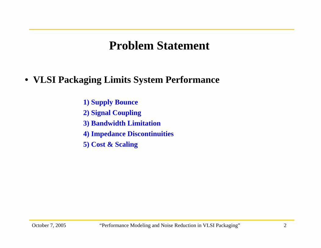
Problem Statement
• VLSI Packaging Limits System Performance
1) Supply Bounce2) Signal Coupling3) Bandwidth Limitation4) Impedance Discontinuities5) Cost & Scaling

October 7, 2005 “Performance Modeling and Noise Reduction in VLSI Packaging” 3
Agenda
1) Problem Motivation
2) Research Overview
3) Advantages Over Prior Techniques
4) Broader Impact of this Work
October 7, 2005 “Performance Modeling and Noise Reduction in VLSI Packaging” 4
1) Problem Motivation
October 7, 2005 “Performance Modeling and Noise Reduction in VLSI Packaging” 5
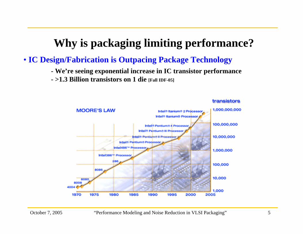
Why is packaging limiting performance?• IC Design/Fabrication is Outpacing Package Technology
- We’re seeing exponential increase in IC transistor performance- >1.3 Billion transistors on 1 die [Fall IDF-05]

October 7, 2005 “Performance Modeling and Noise Reduction in VLSI Packaging” 6
Why is packaging limiting performance?• Packages Have Been Designed for Mechanical Performance
- Electrical performance was not primary consideration- IC’s limited electrical performance- Package performance was not the bottleneck
October 7, 2005 “Performance Modeling and Noise Reduction in VLSI Packaging” 7
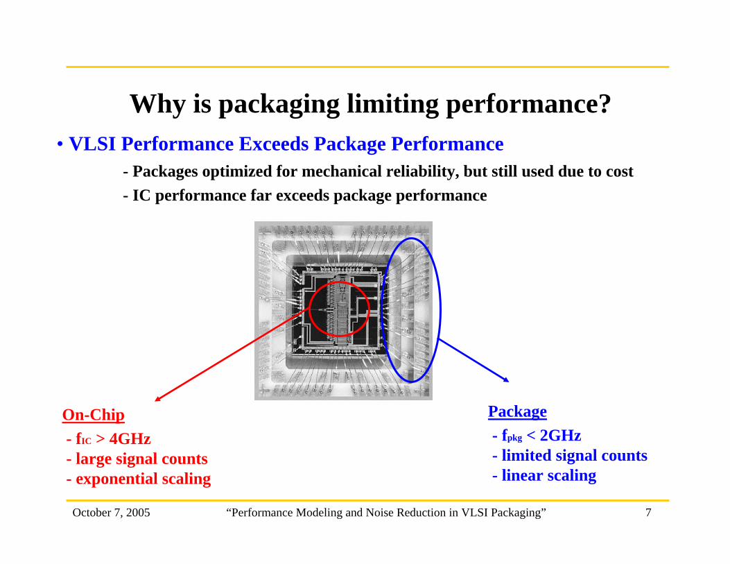
Why is packaging limiting performance?• VLSI Performance Exceeds Package Performance
- Packages optimized for mechanical reliability, but still used due to cost- IC performance far exceeds package performance
On-Chip- fIC > 4GHz- large signal counts- exponential scaling
Package- fpkg < 2GHz- limited signal counts- linear scaling

October 7, 2005 “Performance Modeling and Noise Reduction in VLSI Packaging” 8
Why is packaging limiting performance?• Package Interconnect Contains Parasitic Inductance and Capacitance
- Long interconnect paths
- Large return loops
-
-
Wire Bond Inductance (~2.8nH)
LIΦ
=
Q ACV t
ε= =
BGA Capacitance (~300fF)

October 7, 2005 “Performance Modeling and Noise Reduction in VLSI Packaging” 9
Why is packaging limiting performance?• Package Parasitics Limit Performance
- Excess L and C causes package noise- Noise limits how fast the package can transmit date
1) Supply Bounce2) Signal Coupling3) Bandwidth Limiting4) Impedance Discontinuities

October 7, 2005 “Performance Modeling and Noise Reduction in VLSI Packaging” 10
Why is packaging limiting performance?• Aggressive Package Design Helps, but is expensive…
- 95% of VLSI design-starts are wire bonded- Goal: Extend the life of current packages
QFP – Wire Bond : 4.5nH → $0.22 / pin
BGA – Wire Bond : 3.7nH → $0.34 / pin ***
BGA – Flip-Chip : 1.2nH → $0.63 / pin

October 7, 2005 “Performance Modeling and Noise Reduction in VLSI Packaging” 11
2) Research Overview
October 7, 2005 “Performance Modeling and Noise Reduction in VLSI Packaging” 12
Research Overview
• Performance Modeling & Bus Sizing- algebraic model to predict performance and cost-effectiveness
• Bus Expansion CODEC- encoding data to avoid patterns on bus which cause excessive noise
• Bus Stuttering CODEC- encoding data to avoid patterns on bus which cause excessive noise
• Impedance Compensation- adding C or L near package to match impedance to system

October 7, 2005 “Performance Modeling and Noise Reduction in VLSI Packaging” 13
- “FPGA I/O – When to go serial”, IEE Electronic Systems and Software, 2004
- “Performance Model for Inter-Chip Busses Considering Bandwidth and Cost”DesignCon, 2005
- “Performance Model for Inter-chip Com Considering Inductive Cross-talk and Cost”,ISCAS, 2005
- “Performance Model for Inter-Chip Busses Considering Bandwidth and Cost”,DesignConEast, 2005
- “Package Performance Model for Off-chip Busses Considering Bandwidth and Cost”,IEE Journal on Computers and Digital Techniques (accepted for publication)
Publications: Performance Modeling and Bus Sizing
• Best Paper Award

October 7, 2005 “Performance Modeling and Noise Reduction in VLSI Packaging” 14
- “Encoding-based Minimization of Inductive Cross-talk for Off-chip Data Transmission”, DATE, 2005
- “Controlling Inductive Cross-talk and Power in Off-chip Buses using CODECS”, ASP-DAC 2006 (accepted for publication)
- “Bus Stuttering: An Encoding Technique to Reduce Inductive Noise in Off-Chip Data”, DATE 2006 (submitted)
Publications: Bus CODECs to Avoid Package Noise

October 7, 2005 “Performance Modeling and Noise Reduction in VLSI Packaging” 15
- “Time Domain Analysis of a Printed Circuit Board Via”, Microwave Journal, 2000
- “The Effect of Ground Vias on Changing Signal Layers in Multi-Layered PCBs”, Microwave and Optical Technology Letters, 2001
- “Broadband Impedance Matching for Inductive Interconnect in VLSI Packages”, ICCD, 2005
- “Impedance Matching Techniques for VLSI Packaging”, DesignCon, 2006 (accepted for publication)
Publications: Impedance Compensation
• Best Paper Award
October 7, 2005 “Performance Modeling and Noise Reduction in VLSI Packaging” 16
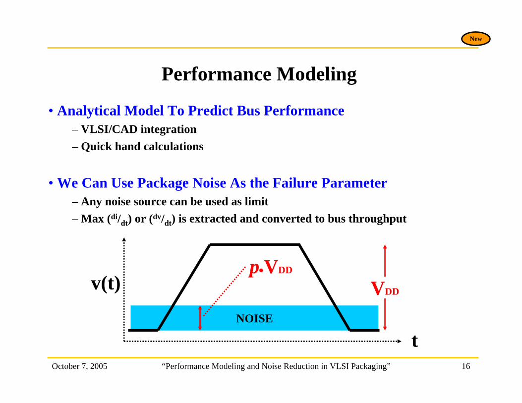
Performance Modeling
• Analytical Model To Predict Bus Performance– VLSI/CAD integration– Quick hand calculations
• We Can Use Package Noise As the Failure Parameter– Any noise source can be used as limit– Max (di/dt) or (dv/dt) is extracted and converted to bus throughput
NOISE
v(t)
t
p•VDD
VDD
New

October 7, 2005 “Performance Modeling and Noise Reduction in VLSI Packaging” 17
Performance Modeling• Bus Notation
- Analysis performed on repetitive segment, reducing computation time- A scalable framework is used to represent the bus configuration
G S PS S S G S S P S S G S SP S S
Wbus
segment (j-1) segment (j) segment (j+1)
M12M12
M13M13
M1(pL) M1(pL)
C12C12
C13C13
C1(pC) C1(pC)
L11 , C0
Mutual Capacitance
Mutual Inductance
Self Inductance, Capacitance
(Ng , Np)
New

October 7, 2005 “Performance Modeling and Noise Reduction in VLSI Packaging” 18
Performance Modeling
• Use Ground Bounce as Failure Mechanism
( )2
1|(| | 1) 0111|(| | 1) 0.8
CL
L C
ppkbus
gnd bnc k DDk p k pk k kg
C ZL W di di diV M p VN dt dt dt
+− +
=− =−
⎛ ⎞ ⎛ ⎞⋅⋅ ⎛ ⎞ ⎛ ⎞ ⎛ ⎞= + ⋅ + ⋅ = ⋅⎜ ⎟ ⎜ ⎟⎜ ⎟ ⎜ ⎟ ⎜ ⎟⎜ ⎟⎜ ⎟⎝ ⎠ ⎝ ⎠ ⎝ ⎠⎝ ⎠⎝ ⎠∑ ∑
Self Contribution
G S PS S S G S S P S S G S S PP S S
Mutual Inductive Contribution
Mutual Capacitive Contribution
NoiseLimit
New

October 7, 2005 “Performance Modeling and Noise Reduction in VLSI Packaging” 19
∴ Slewrate
∴ Risetime
Performance Modeling
dt
dvv(t)
t
loaddv dislewrate Zdt dt
⎛ ⎞ ⎛ ⎞= = ⋅⎜ ⎟ ⎜ ⎟⎝ ⎠ ⎝ ⎠
(0.8)•VDDv(t)
t
90%
10%
VDD
(0.8) DDrise
Vtslewrate
⋅=
New
October 7, 2005 “Performance Modeling and Noise Reduction in VLSI Packaging” 20
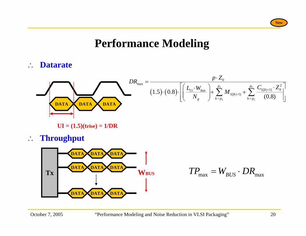
∴ Datarate
∴ Throughput
Performance Modeling
DATADATA DATA
UI = (1.5)(trise) = 1/DR
max maxBUSTP W DR= ⋅
DATADATA DATA
DATADATA DATA
DATADATA DATA
Tx WBUS
( ) ( )
0max 2
1(| | 1) 0111(| | 1)1.5 0.8
(0.8)
CL
L C
ppkbus
kk p k pg
p ZDRC ZL W M
N+
+= =
⋅=
⎡ ⎤⎛ ⎞ ⋅⋅⋅ ⋅ + +⎢ ⎥⎜ ⎟⎜ ⎟⎢ ⎥⎝ ⎠⎣ ⎦
∑ ∑
New

October 7, 2005 “Performance Modeling and Noise Reduction in VLSI Packaging” 21
Performance Modeling
• BGA Wire-Bond Package Simulations
Per-Pin Data-Rate Bus Throughput Model Error
- Model Matches Simulations to 11% for segments greater than 1 bit- Throughput does not increase linearly as channels are added
Simulation Model
New

October 7, 2005 “Performance Modeling and Noise Reduction in VLSI Packaging” 22
Bus Expansion CODEC• Encode the Data To Avoid Noise Causing Vector Sequences
- Reducing noise allows faster per-pin datarate- Throughput is increased even after considering Overhead- Bus Expansion CODEC maps on-chip bus size (m) into off-chip bus size (n)
Package
DATADATA DATA
DATADATA DATA
DATADATA DATA
n-bits (un-encoded)DATADATA DATA
DATADATA DATA
DATADATA DATA
Package n-bits (encoded)
DATADATA DATA
DATADATA DATA
DATADATA DATA
DATADATA DATA
DATADATA DATA
Encoder
Core
Core
m-bits
n-bits
No Encoding
w/ Encoding
Covered in Comps

October 7, 2005 “Performance Modeling and Noise Reduction in VLSI Packaging” 23
• For Each Possible Noise Source on the Bus, a Constraint is written
1) v0j = VDD → - Pbnc > (L/2)· (# of vi
j pins =1) < Pbnc2) v1
j = 1 → k1· (v2j) + k2· (v3
j) > P13) v1
j = -1 → k1· (v2j) + k2· (v3
j) < P-14) v1
j = 0 → - P0 < k1· (v2j) + k2· (v3
j) < P0
• Each Constraint is Evaluated to Find Illegal Transitions:
v1j = 1 = rising v1
j v2j v3
j
v1j = 0 = static ______________
v1j = -1 = falling 1 0 1
1 -1 01 -1 -11 -1 11 1 01 1 -11 1 1
Bus Expansion CODEC - Constraints
violates user-defined “glitch” parameter
violates user-defined “supply” bounce parameter
Covered in Comps

October 7, 2005 “Performance Modeling and Noise Reduction in VLSI Packaging” 24
• The Remaining Legal Transitions Construct a Directed Graph
• The Directed Graph is evaluated to see if an m-bit bus can be encoded- A closed set of nodes S must exist such that:
• |S| > 2m
• each vertex s in S has at least 2m outgoing edges to vertices s’ in S
Bus Expansion CODEC - Algorithm
G
Covered in Comps

October 7, 2005 “Performance Modeling and Noise Reduction in VLSI Packaging” 25
Bus Expansion CODEC – Physical Results
• TSMC 0.13um Synthesis Results- RTL design, synthesized and mapped- Segment sizes 2 8 implemented- Logic, delay, and area evaluated
New

October 7, 2005 “Performance Modeling and Noise Reduction in VLSI Packaging” 26
Bus Expansion CODEC – Physical Results
• Xilinx FPGA, 0.35um Implementation Results- RTL design implemented- Xilinx, VirtexIIPro, FPGA
New

October 7, 2005 “Performance Modeling and Noise Reduction in VLSI Packaging” 27
Bus Expansion CODEC – Physical Results
• Xilinx FPGA, 0.35um Implementation Results- RTL design, implemented- Segment sizes 2 8 measured- Logic operation verified - Noise Reduced from 16% to 4%
(3 bit, SPG=4:1:1)
New
October 7, 2005 “Performance Modeling and Noise Reduction in VLSI Packaging” 28
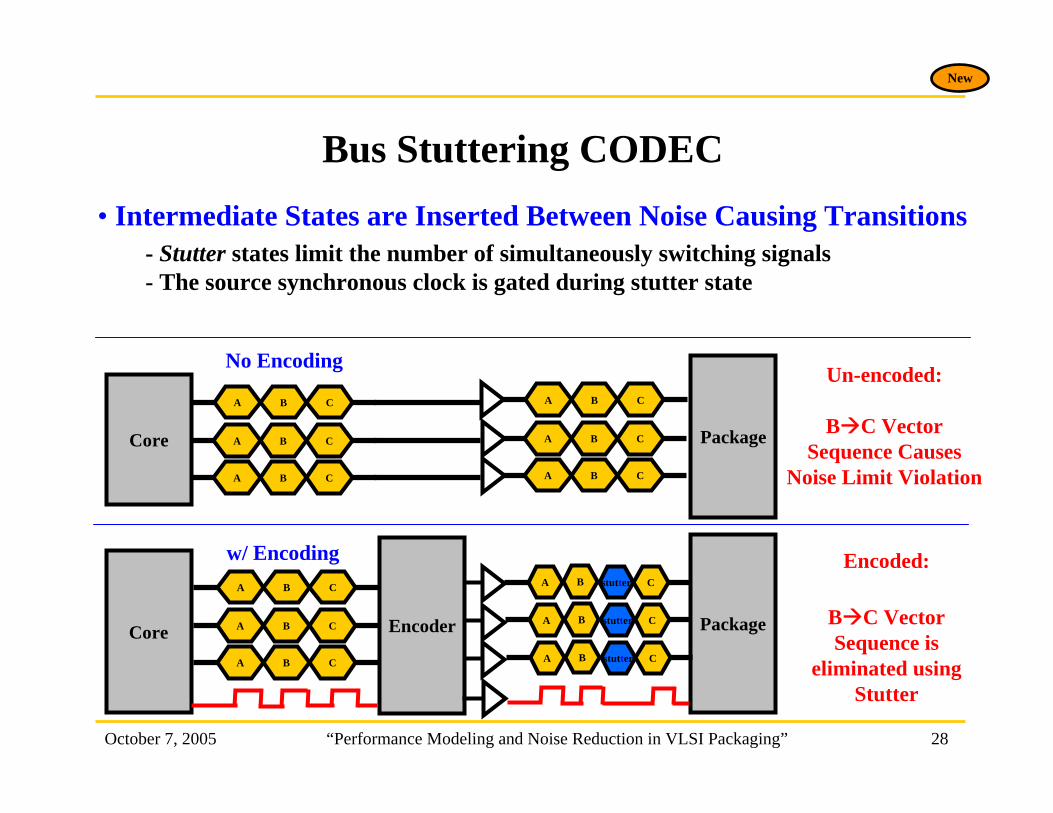
Bus Stuttering CODEC• Intermediate States are Inserted Between Noise Causing Transitions
- Stutter states limit the number of simultaneously switching signals - The source synchronous clock is gated during stutter state
Package
Un-encoded:
B C Vector Sequence Causes
Noise Limit Violation
Package
Encoded:
B C Vector Sequence is
eliminated using Stutter
BA C
BA C
BA C
Encoder
Core
Core
No Encoding
w/ Encoding
BA C
BA C
BA C
BA C
BA C
BA C A B stutter C
A B stutter C
A B stutter C
New
October 7, 2005 “Performance Modeling and Noise Reduction in VLSI Packaging” 29
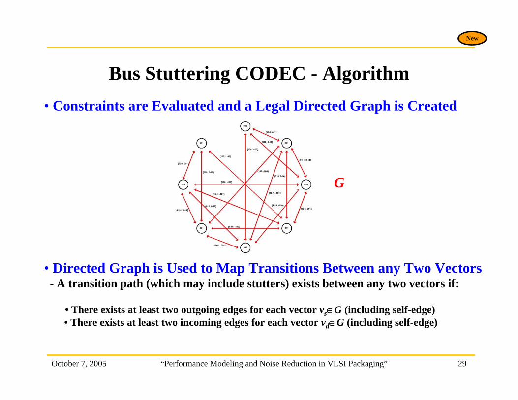
• Constraints are Evaluated and a Legal Directed Graph is Created
• Directed Graph is Used to Map Transitions Between any Two Vectors- A transition path (which may include stutters) exists between any two vectors if:
• There exists at least two outgoing edges for each vector vs∈G (including self-edge)• There exists at least two incoming edges for each vector vd∈G (including self-edge)
Bus Stuttering CODEC - Algorithm
G
New

October 7, 2005 “Performance Modeling and Noise Reduction in VLSI Packaging” 30
Bus Stuttering CODEC - Construction
• Multiple Stutter States can be used- between 0 and 2(Wbus-1) stutters can be inserted between any two vectors- experimental results show that for segments up to 8 bits, more than 3 stutters is rare
• Overhead- Overhead increases as segments sizes increase- Still useful since segments greater than 8 bits are rarely used (SPG=8:1:1)
( 1)2
1(2 )
(#_ _ Re _ _ )
2
Wbus
bus
kW
Trans quiring k stutters kOverhead
−
=⋅
⋅=∑
New

October 7, 2005 “Performance Modeling and Noise Reduction in VLSI Packaging” 31
Bus Stuttering CODEC – Physical Results
• Circuit Implementation- 32 pipeline stages used- pipeline reset after 32 idle states (similar to SRIO, HT, and PCI Express)
- protocol inherently handles pipeline overflow
New

October 7, 2005 “Performance Modeling and Noise Reduction in VLSI Packaging” 32
Bus Stuttering CODEC – Physical Results
• TSMC 0.13um Synthesis Results- RTL design, synthesized and mapped- Segment sizes 2 8 implemented- Logic, delay, and area evaluated
New

October 7, 2005 “Performance Modeling and Noise Reduction in VLSI Packaging” 33
Bus Stuttering CODEC – Physical Results
• Xilinx FPGA, 0.35um Implementation Results- RTL design, implemented- Segment sizes 2 8 measured- Logic operation verified- Noise Reduced from 16% to 4%
(3 bit, SPG=4:1:1)
New

October 7, 2005 “Performance Modeling and Noise Reduction in VLSI Packaging” 34
Impedance Compensation• Add Capacitance Near Bond Wire to Reduce Impedance
- Adding additional capacitance lowers the wire bond impedance- Impedance can be matched to system, reducing reflections
WireBondWireBond
WireBond
LZC
=Add Capacitance to lower Z
0
0
L
L
Z ZZ Z
−Γ =
+Better Impedance Match results in less reflections
Covered in Comps

October 7, 2005 “Performance Modeling and Noise Reduction in VLSI Packaging” 35
Impedance Compensation• If the capacitance is close to the wire bond, it will alter its impedance
- Electrical lengths less than 20% of risetime are treated as lumped elements- For modern dielectrics, anything within 0.15” of wire bond is lumped
Treated as Lumped Element
Treated as Distributed Element
Covered in Comps
October 7, 2005 “Performance Modeling and Noise Reduction in VLSI Packaging” 36
Ccomp2Ccomp1
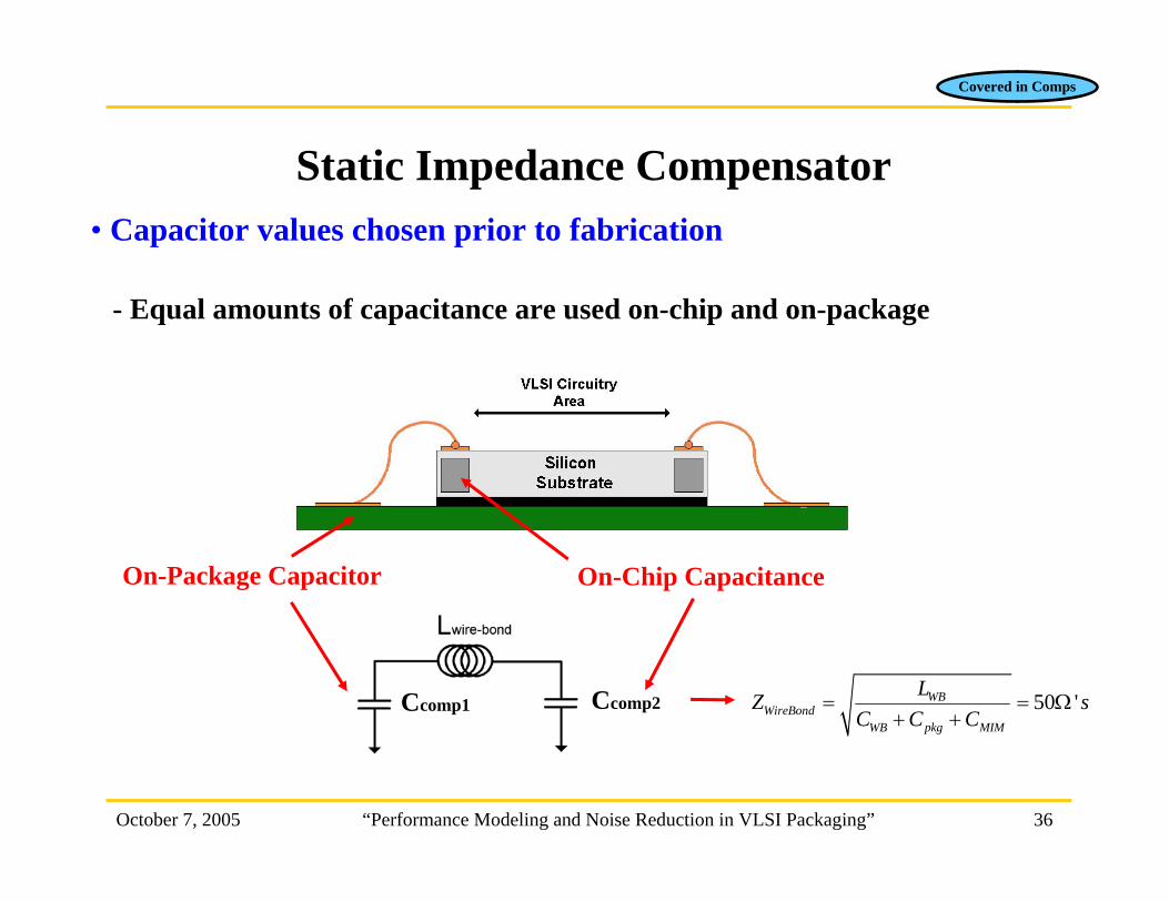
Static Impedance Compensator• Capacitor values chosen prior to fabrication
- Equal amounts of capacitance are used on-chip and on-package
On-Package Capacitor On-Chip Capacitance
50 'WBWireBond
WB pkg MIM
LZ sC C C
= = Ω+ +
Covered in Comps
October 7, 2005 “Performance Modeling and Noise Reduction in VLSI Packaging” 37
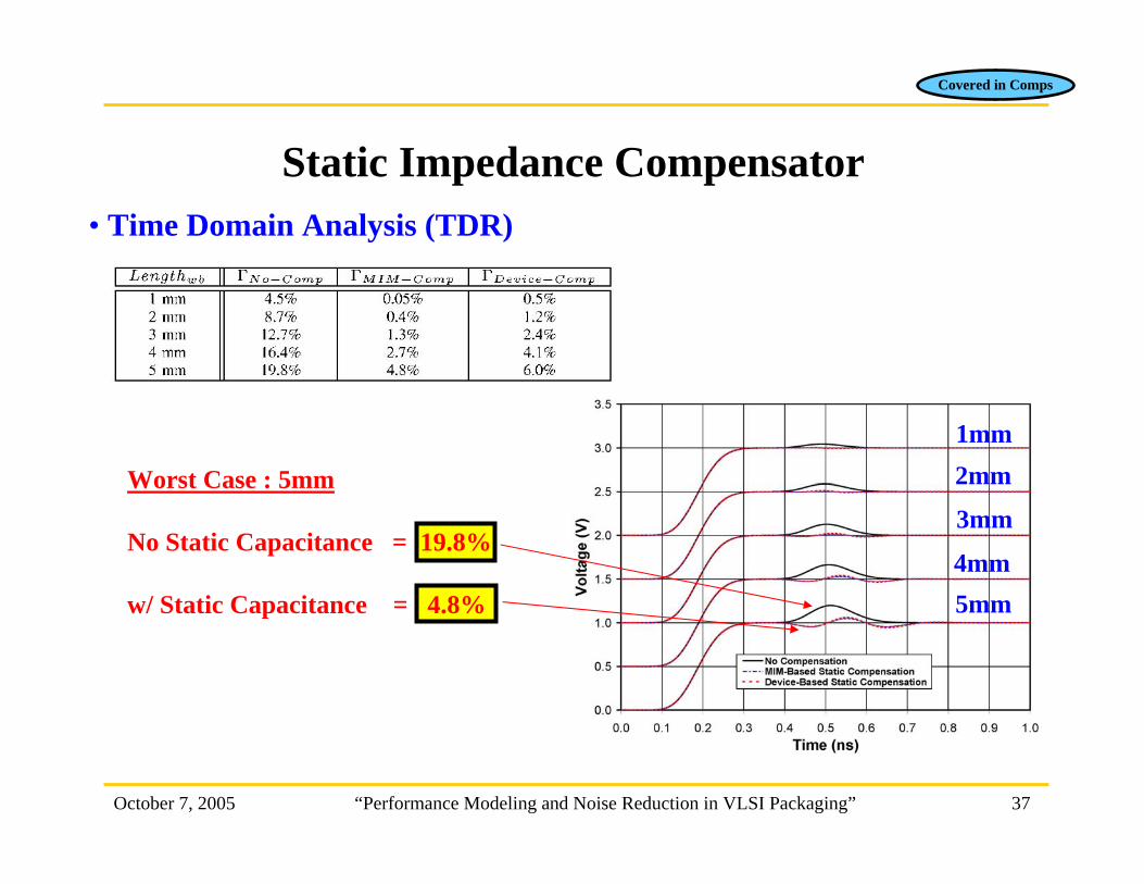
Worst Case : 5mm
No Static Capacitance = 19.8%
w/ Static Capacitance = 4.8%
Static Impedance Compensator• Time Domain Analysis (TDR)
1mm2mm
3mm
4mm5mm
Covered in Comps
October 7, 2005 “Performance Modeling and Noise Reduction in VLSI Packaging” 38
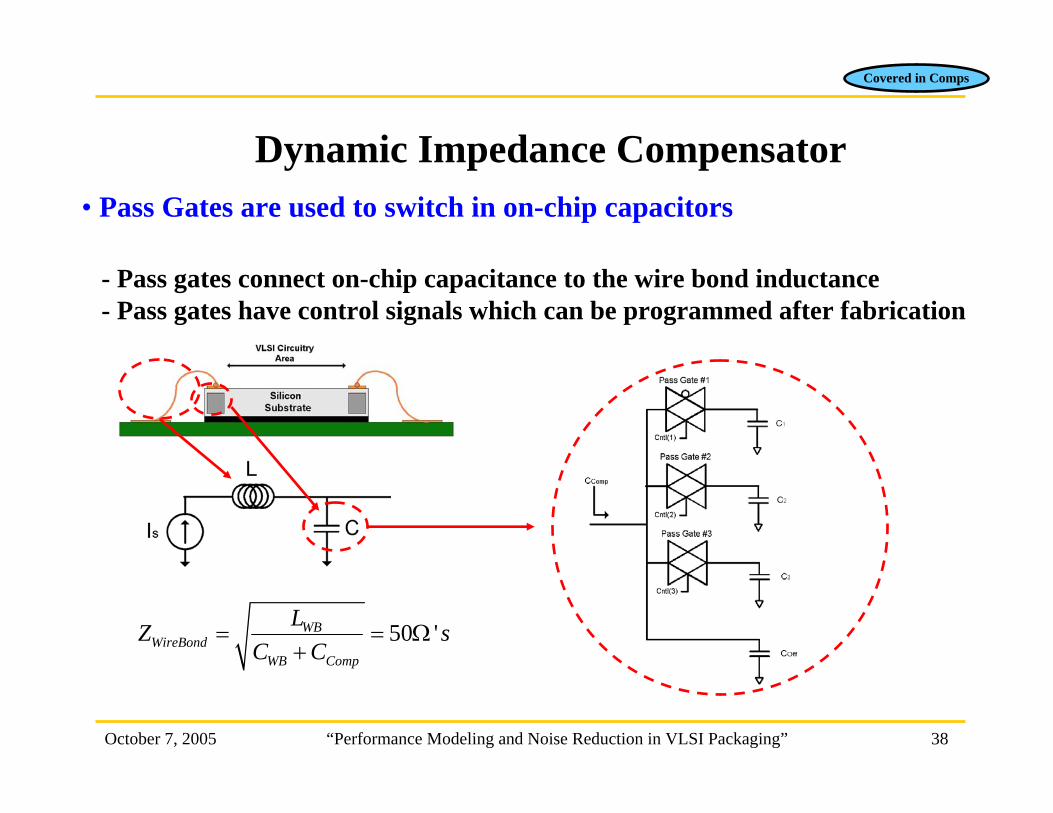
Dynamic Impedance Compensator• Pass Gates are used to switch in on-chip capacitors
- Pass gates connect on-chip capacitance to the wire bond inductance- Pass gates have control signals which can be programmed after fabrication
50 'WBWireBond
WB Comp
LZ sC C
= = Ω+
Covered in Comps

October 7, 2005 “Performance Modeling and Noise Reduction in VLSI Packaging” 39
Worst Case : 5mm
No Dynamic Capacitance = 19.8%
w/ Dynamic Capacitance = 6.0%
Dynamic Impedance Compensator• Time Domain Analysis (TDR)
1mm2mm
3mm
4mm5mm
Covered in Comps
October 7, 2005 “Performance Modeling and Noise Reduction in VLSI Packaging” 40
3) Advantages Over Prior Techniques
Comp Question
October 7, 2005 “Performance Modeling and Noise Reduction in VLSI Packaging” 41
Performance Modeling and Bus Sizing• Currently Packages are Modeled Using SPICE
- Analog simulators are computationally expensive [BSIM, BPTM
- Time of simulation reduces the number of configurations to be evaluated [Agilent Ft. Collins]
• Model is Linear in the size of the bus- Fast computation is enabled using key assumptions- More configurations can be evaluated, which expands usefulness- Narrows hundreds of configurations into 2 or 3 for SPICE evaluation
• Cost is Considered- Analog simulators do not account for cost- This adds even more time to analysis
October 7, 2005 “Performance Modeling and Noise Reduction in VLSI Packaging” 42
Bus CODECs to Avoid Package Noise• Current Approaches Have Physical Limitations
- Operate by reducing (di/dt) or skewing transitions [pipeline_damping, Multi-Level]
- Reducing (di/dt) will ultimately limit performance- Skewing data increases data invalid window, will ultimately limit performance
• Our CODECs operate above the physical layer- Only data vectors are altered - Off-chip drivers are left unchanged, no skewing is necessary- This allows usefulness up to higher frequencies- This also allows implementation in various process and package technologies

October 7, 2005 “Performance Modeling and Noise Reduction in VLSI Packaging” 43
Impedance Compensation• Currently, Package Interconnect is Not Addressed
- Only primary impedance is terminated (i.e., the PCB T-line) [HS_Design, MGT]
- No broadband solution exists
• Our Techniques Target Package Directly- Impedance of wire bond or bumping can be addressed- Broadband operation suited well for digital VLSI
• Static Compensator- Developed using embedded construction, no cost- Simple and requires no active circuitry
• Dynamic Compensator- Accounts for process variation by allowing programmability after fabrication

October 7, 2005 “Performance Modeling and Noise Reduction in VLSI Packaging” 44
4) Broader Applications of this Work
Comp Question

October 7, 2005 “Performance Modeling and Noise Reduction in VLSI Packaging” 45
• 80% of Design Starts Have FPGAs
1992Source: Agilent‘97 ‘98 ‘99 ‘00 ‘01 ‘02
Design Starts per Year
ASIC
FPGA
4x
‘031996 2001 20022004
Xilinx
The Move Toward FPGAs
‘04

October 7, 2005 “Performance Modeling and Noise Reduction in VLSI Packaging” 46
- Single design is packaged in multiple technologies- This enables multiple performance price-points- Designer cannot optimize for particular package
The Move Toward FPGAs• FPGA Business Model
RA
M LUTs
Cores
Wire-Bond Flip-Chip
Cost / Performance
- Performance Modeling- Noise Reduction CODECs- Impedance Compensators

October 7, 2005 “Performance Modeling and Noise Reduction in VLSI Packaging” 47
Power Minimization• Power is Predicted to Limit Moore’s Law
- Large amounts of power are consumed in the off-chip drivers- CODECs can remove patterns which result in noise violations- CODECs can also remove patterns with high power consumption
> 100W [ITRS]
October 7, 2005 “Performance Modeling and Noise Reduction in VLSI Packaging” 48
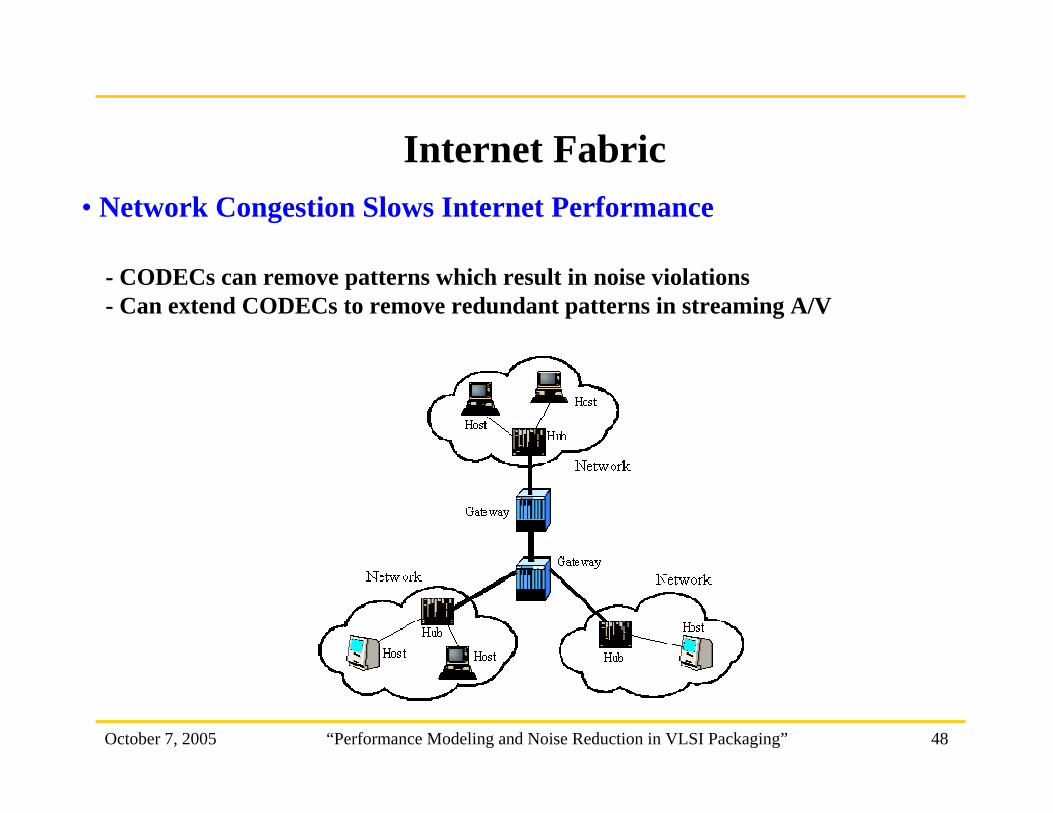
Internet Fabric• Network Congestion Slows Internet Performance
- CODECs can remove patterns which result in noise violations- Can extend CODECs to remove redundant patterns in streaming A/V

October 7, 2005 “Performance Modeling and Noise Reduction in VLSI Packaging” 49
Backplanes and Connectors• All Interconnect Has Parasitic Inductance and Capacitance
- Backplanes are popular to provide design segmentation and scalability- Connectors are present in all digital designs- Modeling, CODECs, and Compensation can be applied to backplanes/connectors

October 7, 2005 “Performance Modeling and Noise Reduction in VLSI Packaging” 50
Questions?