Updated Thermo-Mechanical Model of the CLIC Two-Beam Module Riku Raatikainen 18.7.2011.
L7 1© P. Raatikainen Switching Technology / 2007
PDH Switches
Switching Technology S38.3165http://www.netlab.hut.fi/opetus/s383165
L7 2© P. Raatikainen Switching Technology / 2007
PDH switches
•General structure of a telecom exchange•Timing and synchronization•Dimensioning example

L7 3© P. Raatikainen Switching Technology / 2007
PDH exchange
•Digital telephone exchanges are called SPC (Stored ProgramControl) exchanges
•controlled by software, which is stored in a computer or agroup of computers (microprocessors)
•programs contain the actual intelligence to perform controlfunctions
•software divided into welldefined modular blocks, whichmakes the system less complicated to maintain and expand
•Main building blocks•subscriber interfaces and trunk interfaces•switch fabric•switch/call control
L7 4© P. Raatikainen Switching Technology / 2007
Basic blocks of a PDH exchange
…
LOCALLOOP
SUB
SCR
IBER
INTE
RFA
CE
SWITCHFABRIC
TRU
NK
INTE
RFA
CE
SWITCH CONTROL
…

L7 5© P. Raatikainen Switching Technology / 2007
Switch control
•Centralized•all control actions needed to set up/tear down a connection
are executed in a central processing unit•processingwork normally shared by a number of processors•hierarchical or nonhierarchical processor architecture
•Distributed•control functions are shared by a number of processing units
that are more or less independent of one another•switching device divided into a number of switching parts and
each of them has a control processor
L7 6© P. Raatikainen Switching Technology / 2007
Switch control (cont.)
… …
ControlprocessorControl
processor
Centralized nonhierarchicalprocessor system
Control units usually doubled or tripled
RP
Centralprocessor
RP…
……
Centralized hierarchicalprocessor system
RP Regional Processor

L7 7© P. Raatikainen Switching Technology / 2007
Switch control (cont.)
Switching partwith controlprocessor…
Switching partwith controlprocessor…
Switching partwith controlprocessor …
Switching partwith controlprocessor …
Distributed controlwith independent switching parts
L7 8© P. Raatikainen Switching Technology / 2007
Example construction of a PDHexchange
…
NT
SWITCHFABRIC
CONTROLPROCESSOR
…
ET
TRUNKINTERFACES
ET
AUX
SUBSCRIBERINTERFACES
NT
…
AUX Auxiliary equipmentET Exchange TerminalNT Network Terminal
ADMINISTRATIONCOMPUTER
SWITCHING &CALL CONTROL

L7 9© P. Raatikainen Switching Technology / 2007
Example of call control processing
CCSUCCSULSULSURURUSSUSSU RU LSU CCSUSSU
STUSTUCMCMMMM CM STU
CCSU Common Channel Signaling UnitCM Central MemoryLSU Line Signaling UnitM Marker
RU Registering UnitSSU Subscriber Stage UnitSTU Statistics Unit
DX200 / Nokia
L7 10© P. Raatikainen Switching Technology / 2007
Call processing units
•Common Channel Signaling Unit (CCSU)•processes SS7 signaling messages
•Central Memory (CM)•common central memory of the different control units
•Line Signaling unit (LSU)•processes line signaling information
•Marker (M)•connection (channel) control
•Register Unit (RU)•registers for information such as call/customer related billing
•Subscriber Stage Unit (SSU)•subscriber stage control (incl. subscriber signaling)
•Statistics Unit (STU)•statistical information such as call durations and outage periods

L7 11© P. Raatikainen Switching Technology / 2007
Hierarchical control software
Administrationprograms
Call controlprograms
Signaling messageprocessing
Software systems in the control part: signaling and call control charging and statistics maintenance software
Control of connections: calls should not be directed to faulty destinations faulty connections should be cleared detected faulty connections must be reported tofarend if possible
L7 12© P. Raatikainen Switching Technology / 2007
Switching part
•Main task of a switching part is to connect an incoming timeslotto an outgoing one –unit responsible for this function is called agroup switch
•Control system assigns incoming and outgoing timeslot, whichare reserved by signaling, on associated physical links=> need for time and space switching
Group switch
A
B
2
1
2
1

L7 13© P. Raatikainen Switching Technology / 2007
Group switch implementations
•Group switch can be based on a space or time switch fabric•Memory based time switch fabrics are the most common ones
flexible construction due to advances in IC technology suitable also for large switch fabrics
123
...
Timeslot counter & R/W controlTimeslot counter & R/W control
...k
m
Switchmemory
123
n
Controlmemory
...
...j (k)
123m …Incoming frame buffer
12jn … …Outgoing frame buffer
Cyclic read
writ
ead
dres
s (3
)
read
/writ
ead
dres
s (j)read
address (k)
Cyclic write
L7 14© P. Raatikainen Switching Technology / 2007
Subscriber connections
…
Remotesubscriber
switch
……
Subscribermux
Groupswitch
Local exchange
…
Subscriberswitch

L7 15© P. Raatikainen Switching Technology / 2007
Typical subscriber connections andtrunk lines
•Subscriber connections•conventional twisted pair serving, e.g., an analog 3 kHz voice
channel or 2B+D digital ISDN connection•radio link serving, e.g., an analog voice channel (NMT) or a
digital GSM voice/data channel•E1, … , E3 links connecting business users with a number of
voice channels•Trunk lines
•standard PDH links (E1, … , E4)•standard SDH links (STM1, ..., STM16) carrying standard
PDH/PCM signals•new technology approaching, e.g, OTN and 1 Gbit/s Ethernet
L7 16© P. Raatikainen Switching Technology / 2007
Subscriber and trunk interface
•Subscriber interface•onhook/offhook detection, reception of dialed digits•check of subscriber line, power supply for subscriber line•physical signal reception/transmission, A/Dconversion•concentration
•Trunk interface•timing and synchronization (bit and octet level) to line/clock
signal coming from an exchange of higher level of hierarchy•frame alignment/frame generation•multiplexing/demultiplexing

L7 17© P. Raatikainen Switching Technology / 2007
Example of telephone network hierarchy
Localexchange
Tandemlevel
Regionaltransit level
Nationaltransit level
Internationaltransit level
L7 18© P. Raatikainen Switching Technology / 2007
2.5G/3G mobile network architecture
BSCPCUBS
BS
BS
MSC
SN
HLR
GN
PSTN
2.5G/3GBACKBONE INTERNET
BS Base StationBSC Base Station ControllerGN Gateway NodeHLR Home Location Register
MSC Mobile Switching CentrePCU Packet Control UnitSN Support Node

L7 19© P. Raatikainen Switching Technology / 2007
Intelligent network
•Conventional telecommunications network supports plain circuitswitching allowing only point to point connectivity
•Intelligence of a telecommunications network can be enhancedby implementing Intelligent Network (IN) architecture for servicedevelopment, control and management
•IN allows for an operator to offer enriched services, such as calldiversion on no answer or on busy, multiparty conference orabbreviated dialing
•IN is a telecommunications network architecture, which offersopen, distributed and service independent platform forimplementing supplementary services in a telecom network
L7 20© P. Raatikainen Switching Technology / 2007
IN network functions and elements
•IN concept separates service control function (SCF) logicallyfrom service switching function (SSF) and from call control(CCF) and switching functions
•Service Control Point (SCP), which implements SCF, is acentrally located node that contains logic and data for INservices
•SCP receives requests from SSP, executes services requestedand returns information to SSP
•Service Switching Point (SSP), which implements SSF, is anode that detects calls to IN service
•SSP communicates with SCP to obtain information on how toset up connections related to an IN call

L7 21© P. Raatikainen Switching Technology / 2007
IN network functions and elements
•SSP and SCP communicate via Signaling Transfer Point (STP),which usually is the common channel signaling network
•Service Management System (SMS) is an administrative supportsystem for the development and handling of new services in thetelephone network
•Intelligent Peripheral (IP) is used for some valueadded servicesto enable communication between the IN functions andsubscriber, e.g., reception of DTFM signals and transmission ofvoice messages.
•IP is activated by SSP at the request of SCP
L7 22© P. Raatikainen Switching Technology / 2007
Intelligent network architecture
INAP IN Application ProtocolIP Intelligent PeripheralPSTN Public Switched Telephone NetworkSCE Service Creation EnvironmentSCP Service Control PointSDP Service Data Point
SMS Service Management SystemSSP Service Switching Point
SMS
SCP
SSP SSP
SCE
IPIP
PSTN
SDP

L7 23© P. Raatikainen Switching Technology / 2007
IN service creation
•Logical separation of service control functions from call control andswitching functions allows such service implementations that wouldbe complicated and would consume excessively network resourcesif they were implemented in switching equipment
•Service Creation Environment (SCE) is used for servicedevelopment and SMS is used for injecting the new services intoSCP
•IN services are built up of small modules, Service Building Blocks(SIBs), which have well defined interfaces
•SIBs are presented as graphical symbols, which are interconnectedin a desired way to build up the logic of a service result is a script
•A script can be the logic of a complete service, but a service usuallyconsists of several scripts
L7 24© P. Raatikainen Switching Technology / 2007
Network synchronization
Need for synchronization•Today’s digital telecom networks are combination of PDH and
SDH technologies, i.e. TDM and TDMA utilized•These techniques require that time and timing in the network can
be controlled, e.g., when traffic is added to or dropped from a bitstream in an optical fiber or to/from a radiotransmitted signal
•The purpose of network synchronization is to enable the networknodes to operate with the same frequency stability and/orabsolute time
•Network synchronism is normally obtained by applying themasterslave timing principle

L7 25© P. Raatikainen Switching Technology / 2007
Network synchronization (cont.)
Methods for network synchronization•Distribute the clock over special synchronization links
– offers best integrity, independent of technological development andarchitecture of the network
•Distribute the clock by utilizing traffic links– most frequently used (masterslave network superimposed on the
traffic network)•Use an independent clock in each node
– expensive method, but standard solution in international exchanges•Use an international navigation system in each node
– GPS (Global Positioning System) deployed increasingly– independent of technological development and architecture of network
•Combine some of the above methods
L7 26© P. Raatikainen Switching Technology / 2007
Masterslave synchronization overtransport network
Localexchange level
Transit level
International level
Remotesubscriber switch
∼∼
Highstabilityreference clocks
ITUT Recommendations G.810, G.811, G.812, G.812, G.823

L7 27© P. Raatikainen Switching Technology / 2007
SDH synchronization networkreference chain
•As the number of clocks in tandem increases, synchronization signal isincreasingly degraded
•To maintain clock quality, it is important to specify limit to the number ofcascaded clocks and set limit on degradation of the synchronization signal
•Reference chain consists of K SSUs each linked with N SECs•Provisionally K and N have been set to be K=10 and N=20
total number of SECs has been limited to 60
PRC SSU SSU
N x SEC N x SEC N x SEC1st
SSU
N x SEC2nd Kth
PRC Primary Reference Clock (accuracy 1011)SEC SDH Equipment Clock (accuracy 109)SSU Synchronization Supply Unit (accuracy 106)
L7 28© P. Raatikainen Switching Technology / 2007
PDH synchronization referenceconnection
•Endtoend timing requirements are set for the reference connection•Link timing errors are additive on the endtoend connection•By synchronizing the national network at both ends, timing errors can be
reduced compared to totally plesiochronous (separate clock in eachswitch) operation
•International connections mostly plesiochronous
X
LEX
PCX
SCX
TCX
ISC... X
ISCX
ISCX
TCX
SCX
PCX
LE
Nation network Nation networkInternationalnetworkLocal Local
27 500 km
LE Local ExchangePC Primary ExchangeSC Secondary Exchange
TC Tertiary ExchangeISC International Switching Center
X Digital exchange Digital link

L7 29© P. Raatikainen Switching Technology / 2007
Types of timing variation
•Frequency offset steadystate timing difference causes buffer overflows
•Periodic timing differences jitter (periodic variation > 10 Hz) wander (periodic variation < 10 Hz)
•Random frequency variation cased by electronic noise in phaselocked loops of timing devices andrecovery systems transients caused by switching from one clock source to another
•Timing variation causes slips (= loss of a frame or duplication of a frame) in PDH systems pointer adjustments in SDH systems => payload jitter=> data errors
L7 30© P. Raatikainen Switching Technology / 2007
Visualization of jitter and wander
Jitte
r am
plitu
de
t

L7 31© P. Raatikainen Switching Technology / 2007
Timing variation measures
•Time interval error (TIE)– difference between the phase of a timing signal and phase of a
reference (master clock) timing signal (given in ns)•Maximum time interval error (MTIE)
– maximum value of TIE during a measurement period•Maximum relative time interval error (MRTIE)
– underlying frequency offset subtracted from MTIE•Time deviation (TDEV)
– average standard deviation calculated from TIE for varying windowsizes
L7 32© P. Raatikainen Switching Technology / 2007
Maximum time interval error
•Maximum of peaktopeak difference in timing signal delay during ameasurement period as compared to an ideal timing signal
Measurement period ( S )
MTIE
timin
g de
lay
com
pare
d to
idea
l sig
nal
t

L7 33© P. Raatikainen Switching Technology / 2007
MTIE limits for PRC, SSU and SEC
Clocksource
PRC
SSU
SEC
MTIE
25 ns0.3t ns300 ns
0.01t ns
25 ns10t ns
2000 ns433t 0.2 + 0.01t ns
250 ns100t ns2000 ns
433t 0.2 + 0.01t ns
Observationinterval
0.1 < t < 83 s83 < t < 1000 s
1000 < t < 30 000 st > 30 000 s
0.1 < t < 2.5 s2.5 < t < 200 s
200 < t < 2 000 st > 2 000 s
0.1 < t < 2.5 s2.5 < t < 20 s
20 < t < 2 000 st > 2 000 s
ETS 300 4623
L7 34© P. Raatikainen Switching Technology / 2007
Occurrence of slips
•Slips occur on connections whose timing differs from the timing signal usedby the exchange
•If both ends of a connection are internally synchronized to a PRC signal,theoretically slips occur no more frequently than once in 72 days
•In a reference connection, a slip occurs theoretically once in 72/12 = 6days or if national segments are synchronized once in 72/4 = 18 days
•Slip requirement on an endtoend connection is looser:
Average frequency of slips
≤ 5 slips / 24h
5 slips/ 24 h … . 30 slips/ 1h
≤ 10 slips / 1h
Share of time during one year
98.90 %
< 1 %
< 0.1 %

L7 35© P. Raatikainen Switching Technology / 2007
Slip calculation example
Show that two networks with single frame buffers and timed fromseparate PRCs would see a maximum slip rate of one slip every72 days
Solution:•Timing accuracy of a PRC clock is 1011
•Let the frequencies of the two ends be f1 and f2•In the worst case, these frequencies deviate from the reference
clock fo by 1011x fo and those deviations are to different directions•Let the frequencies be f1 = (1+ 1011) fo and f2 = (1 1011) fo
•Duration of bits in these networks are T1= 1/ f1 and T2= 1/ f2
L7 36© P. Raatikainen Switching Technology / 2007
Slip calculation example (cont.)
Solution (cont.):•During one bit interval, the timing difference is T1 T2 and after
some N bits the difference exceeds a frame length of 125 µs and aslip occurs => NT1 T2 = 125x106
=> N = 125x106 / [ T1 T2 ] = 125x106 /[(1/ f1 1/ f2) ]
•Inserting f1 = (1+ 1011) fo and f2 = (1 1011) fo into the above equation,we get => N = 125x106 fo (1 1022)/(2x 1011) = 62.5 x 10 5 x fo
•Multiplying N by the duration (Tb) of one bit, we get the time (Tslip)between slips
•In case of E1 links, fo= 2.048x10⁶/s and Tb = 488 ns. Dividing theobtained Tslip by 60 (s), then by 60 (min) and finally by 24 (h) we getthe average time interval between successive slips to be 72.3 days
L7 37© P. Raatikainen Switching Technology / 2007
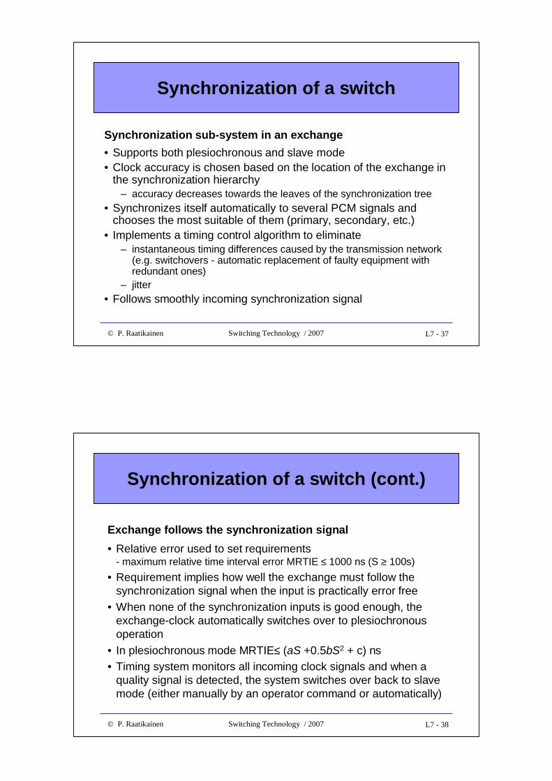
Synchronization of a switch
Synchronization subsystem in an exchange•Supports both plesiochronous and slave mode•Clock accuracy is chosen based on the location of the exchange in
the synchronization hierarchy– accuracy decreases towards the leaves of the synchronization tree
•Synchronizes itself automatically to several PCM signals andchooses the most suitable of them (primary, secondary, etc.)
•Implements a timing control algorithm to eliminate– instantaneous timing differences caused by the transmission network
(e.g. switchovers automatic replacement of faulty equipment withredundant ones)
– jitter•Follows smoothly incoming synchronization signal
L7 38© P. Raatikainen Switching Technology / 2007
Synchronization of a switch (cont.)
Exchange follows the synchronization signal•Relative error used to set requirements
maximum relative time interval error MRTIE ≤ 1000 ns (S ≥ 100s)•Requirement implies how well the exchange must follow the
synchronization signal when the input is practically error free•When none of the synchronization inputs is good enough, the
exchangeclock automatically switches over to plesiochronousoperation
•In plesiochronous mode MRTIE≤ (aS +0.5bS2 + c) ns•Timing system monitors all incoming clock signals and when a
quality signal is detected, the system switches over back to slavemode (either manually by an operator command or automatically)

L7 39© P. Raatikainen Switching Technology / 2007
Stability of an exchange clock
•Clock stability is measured by aging (= b) temperature stabilized aging in the order of n x 1010/day
•MRTIE ≤ (aS +0.5bS2 + c) ns S = measurement period a = accuracy of the initial setting of the clock b = clock stability (measured by aging) c = constant
a
b
c
Transit node clock0.5 corresponds to an initial
frequency shift of 5x10¹⁰
1.16x10⁵ correspondsto aging of 109/days
1000
Local node clock10.0 corresponds to an
initial frequency shift of 1x10⁸
2.3x10 4 correspondsto aging of 2x10⁸ /days
1000
L7 40© P. Raatikainen Switching Technology / 2007
MRTIE in an exchange(plesiochronous mode)
1E+0
1E+1
1E+2
1E+3
1E+4
1E+5
1E+6
1E+7
1E+8
1E+9
1E+10
1E+2 1E+3 1E+4 1E+5 1E+6 1E+7
MR
TIE
ns
Observation time (S)
Transit exchange
Local exchange
Duration of a timeslot in an E1 PCMsignal is 3.9 µs and duration of a bit is 488 ns.

L7 41© P. Raatikainen Switching Technology / 2007
Example of SRAM based PDHswitch fabric
Timeinterchangebased 64 PCM switch
4xE1
2M 8M
4xE2 4xE3
34M 140M
…E4
=>
64 x
E1
dem
ux
64 x
E1
=> E
4 m
ux…
L7 42© P. Raatikainen Switching Technology / 2007
Example of SRAM based PDHswitch fabric (cont.)
Memory size and speed requirement:•Switch memory (SM) and control memory (CM) are both single chip
solutions•Size of both SM and CM ≥ 64x32 octets = 2048 octets•Number of SM write and read cycles during a frame interval (125 µs)
is 2x64x32 = 4096•Access cycle of SM should be ≤ 125 µs / 4096 = 30,5 ns•Number of CM write and read cycles during a frame interval (125 µs)
is 1x64x32 = 2048•Access cycle of CM should be ≤ 125 µs / 2048 = 61 ns

L7 43© P. Raatikainen Switching Technology / 2007
PDH bit rates and related bit/octet times
Hierarchylevel
E1/2M
E2/8M
E3/34M
Timeslotinterval [ns]
3906
947
233
Bit interval[ns]
488
118
29
E4/140M 57.4 7.2
•When timeslots turn into parallel form (8 bits in parallel) memoryspeed requirement decreased by a factor of 8
•Present day memory technology enables up to 256 PDH E1 signalsto be written to and read from a SRAM memory on wire speed
L7 44© P. Raatikainen Switching Technology / 2007
Properties of full matrix switches
Pros•strictsense nonblocking•no path search a connection can always be written into the
control memory if requested output is idle•multicast capability•constant delay•multislot connections possible
Cons•switch and control memory both increase in square of the number
of input/outputs•broadband required memory speed may not be available

L7 45© P. Raatikainen Switching Technology / 2007
Make full use of available memory speed
•At the time of design, select components that give adequate performance will stay on the market long enough are not too expensive (often price limits the use of the fastest components)
•To make full use of available memory speed, buses must be fast enough•When increasing required memory speed, practical bus length decreases
(proportional to inverse of speed)
5 ns 20 ns
$/SRAM
DRAM: 20 ... 70 ns
Bus Bitrate
Memory speed Length of a bus
Bus bitrate
L7 46© P. Raatikainen Switching Technology / 2007
Power consumption avoid heatingproblem
•Power consumption of an output gate is a function of inputs connected to it (increased number of inputs => increased powerconsumption) bit rate/clock frequency (higher bit rate => increased power consumption) bus length (long buses inside switch fabric => increased power consumptionand decreased fanout)
•Increase in power consumption => heating problem•Power consumption and heating problem can be reduced, e.g. by using lower
voltage components (higher resolution receivers)
Bus length
Fan
out
Pow
er
Fanout Receiver’s resolution
Pow
er

L7 47© P. Raatikainen Switching Technology / 2007
Logical structure of a full matrix switch
1
2
3
N
1
2
3
N
. . .
. . .
Feasible SMwith availablecomponents
Feasible SMwith availablecomponents
Feasible SMwith availablecomponents
. . .
Replication of inputs Multiplexed inputs
N = 2n
L7 48© P. Raatikainen Switching Technology / 2007
Example of a matrix switch (DX200)
Read
32x64=2k
Address
8
0
7 ...
16Wr
Fanout=32
Control & switching memory card
...
0 63
S/P
Bus buffer
0 63
S/P
0 63
S/P
0 63
S/P
P/S
0
63
CMSM SM SMSM
P/S
0
63
CMSM SM SMSM
P/S
0
63
CMSM SM SMSM
P/S
0
63
CMSM SM SMSM

L7 49© P. Raatikainen Switching Technology / 2007
Example of a matrix switch (cont.)
•S/P (Serial/Parallel conversion) incoming timeslots are turned intoparallel form to reduce the speed on internal buses
•P/S (Parallel/Serial conversion) parallel form output signals convertedback to serial form
•64 PCM S/PP/S pairs implemented on one card, which is practicalbecause PCMs are bidirectional
•One switch block (SB) can serve max 4 S/PP/S pairs which is chosenbased on required capacity (64, 128, 192 or 256 E1s/SB)
•One S/P+P/S pair feeds max 8 parallel switch blocks chosen based onthe required capacity in the installation (n * 256 E1s/SB, 1≤n≤8)
•Max size of the example DX200system fabric is 2048 E1s•Currently, a bigger matrix ( 8K E1s) is available, slightly different SRAMs
are needed, but principle is similar
L7 50© P. Raatikainen Switching Technology / 2007
Example of a matrix switch (cont.)
•A timeslot is forwarded from an S/P to all parallel switch blocks and(in each switch block) it is written to all SMs along the vertical bus
•A single timeslot replicated into max 4x8=32 locations•Data in CMs direct storing of a timeslot in correct positions in SMs•CM also includes data which directs reading of a correct timeslot to
be forwarded to each output timeslot on each output E1 link•CM includes a 16bit pointer to a timeslot to be read
– 2 bits of CM content point to an SM chip and– 5 + 6 = 11 bits point to a memory location on an SM chip– remaining 3 bits point to (source) switch block

L7 51© P. Raatikainen Switching Technology / 2007
Example of a matrix switch (cont.)
•Number of timeslots to be switched during a frame (125 µs): 8x4x64x32 = 65 536 timeslots (= 64 kbytes)
•Each timeslot stored in 4 SMs in each of the 8 switch blocks=> max size of switch memory 8x4x65 536 = 2097152 (= 2 Mbytes)
•Every 32nd memory location is read from SM in a max size switch=> average memory speed requirement < 31 ns (less than theworst case requirement 64x32 write and 64x32 read operationsduring a 125 µs period)
•Control memory is composed of 4x4 control memory banks in eachof the 8 switch blocks and each memory bank includes 2.048kwords (word= 2 bytes) for write and 2.048 kwords for read control,i.e. max CM size is 8x4x4x8kbytes = 1048576 bytes (= 1 Mbytes)
L7 52© P. Raatikainen Switching Technology / 2007
Growth of matrix
256 PCM
512 PCM