Study of Microstructure and Elemental Micro … and Elemental Micro-composition of ZnO:Al Thin Films...
10
ROMANIAN JOURNAL OF INFORMATION SCIENCE AND TECHNOLOGY Volume 14, Number 4, 2011, 346–355 Study of Microstructure and Elemental Micro-Composition of ZnO:Al Thin Films by Scanning and High Resolution Transmission Electron Microscopy and Energy Dispersive X-Ray Spectroscopy E. VASILE 1 , R. PLUGARU 1 , S. MIHAIU 2 , A. TOADER 2 1 National Institute for Research and Development in Microtechnologies-IMT Bucharest, Romania E-mail: [email protected] 2 I. G. Murgulescu Institute of Physical Chemistry, Romanian Academy, Bucharest, Romania Abstract. The microstructure and micro-composition of ZnO thin films doped with Al, deposited on Si/SiO 2 substrates by sol-gel method were inves- tigated by scanning and high resolution transmission electron microscopy and related energy dispersive X-ray analyses (SEM-EDX, STEM-HRTEM/EDX). Thin films of ZnO were prepared by deposition of 1-10 successive layers with 0.5 at.% and 5 at.% Al concentrations. The evolution of the elemental compo- sition, especially the Al concentration and distribution in the films with various number of layers were determined from energy dispersive X-ray spectra (EDS). The qualitative composition of the structures observed in the films have been evidenced in the elemental EDS maps. Keywords: Al-doped ZnO films, sol-gel, nanostructures, SEM-EDX, HRTEM- EDX, STEM-EDX, elemental composition, elemental mapping.
Transcript of Study of Microstructure and Elemental Micro … and Elemental Micro-composition of ZnO:Al Thin Films...
ROMANIAN JOURNAL OF INFORMATIONSCIENCE AND TECHNOLOGYVolume 14, Number 4, 2011, 346–355
Study of Microstructure and Elemental
Micro-Composition of ZnO:Al Thin Films
by Scanning and High Resolution
Transmission Electron Microscopy andEnergy Dispersive X-Ray Spectroscopy
E. VASILE1, R. PLUGARU1, S. MIHAIU2, A. TOADER2
1National Institute for Research and Developmentin Microtechnologies-IMT Bucharest, Romania
E-mail: [email protected]. G. Murgulescu Institute of Physical Chemistry,
Romanian Academy, Bucharest, Romania
Abstract. The microstructure and micro-composition of ZnO thin films
doped with Al, deposited on Si/SiO2 substrates by sol-gel method were inves-
tigated by scanning and high resolution transmission electron microscopy and
related energy dispersive X-ray analyses (SEM-EDX, STEM-HRTEM/EDX).
Thin films of ZnO were prepared by deposition of 1-10 successive layers with
0.5 at.% and 5 at.% Al concentrations. The evolution of the elemental compo-
sition, especially the Al concentration and distribution in the films with various
number of layers were determined from energy dispersive X-ray spectra (EDS).
The qualitative composition of the structures observed in the films have been
evidenced in the elemental EDS maps.
Keywords: Al-doped ZnO films, sol-gel, nanostructures, SEM-EDX, HRTEM-
EDX, STEM-EDX, elemental composition, elemental mapping.

Microstructure and Elemental Micro-composition of ZnO:Al Thin Films 347
1. Introduction
A wide range of applications, such as transparent conductors, electronic devices,UV detectors, solar cells, made that ZnO:Al doped thin films to be the subject ofextensive studies in recent years [1–4]. A significant improvement of the films con-ductivity has been achieved by doping with group III elements: B, Al, Ga, In. Amongthem, Al has been proved as an excellent dopant, leading to a resistivity values of1.2×10−4 Ω cm of sol-gel deposited films with 1.0 at.% dopant concentration [5].It was reported that there is an optimum in the conductivity of ZnO thin films in-creasing by Al doping, explained by a limited incorporation of aluminium atoms intothe ZnO lattice [6, 7]. Previous studies evidenced that structural characteristics andphysical properties of sol–gel deposited ZnO:Al films are strongly affected by solsconcentration with the dopant metal [8]. For instance, experimental results showedthat aluminium concentration affect the crystallite size, determining the deteriora-tion of the films crystallinity. The excessive dopant concentration did not enhancedcarrier concentration, moreover it reduced the mobility, perhaps due to the higherprobability of the impurity scattering [9]. Also, Al3+ dopants segregation into thegrain boundary regions could be observed and found to determine the formation ofan amorphous phase in polycrystalline Al doped ZnO thin film deposited on Si [10].
In this study we investigate the compositional homogeneity of ZnO:0.5% and5% at. Al doped thin films deposited by sol-gel process on Si/SiO2substrates. Energydispersive X-ray analysis in the Scanning Electron Microscopy (SEM-EDX), Scanningand High Resolution Transmission Electron Microscopy (TEM-STEM-HRTEM/EDX)as well as Energy dispersive X-ray spectroscopy (EDS) mapping have been used toassess the nanoscale composition and local distribution of elements in the polycrys-talline films.
2. Experimental
ZnO thin films were deposited on Si/SiO2 substrates by sol-gel method. The Alconcentration was 0.5% at. and 5% at. The flowchart of the sol-gel deposition processwas previously reported [11] and optical and electrical characteristics of the films with1-10 layers were measured and reported [12]. The structural characteristics of the filmswere studied by X-ray diffraction (XRD) (Rigaku SmartLab with Cu Kα radiation)[12]. The microstructure and micro-composition of the films were investigated byscanning electron microscopy and energy dispersive X-ray (EDX) analysis using aSEM Quanta INSPECT F electron microscope, equipped with field emission gun –FEG with a resolution of 1.2 nm and a spectrometer for energy dispersive X-rayspectrometry (EDXS) with resolution of 133 eV to Mn Kα. The films structure andelemental composition analyses at nanoscale were performed using a high resolutiontransmission electron microscope TEM/STEM/HRTEM, TECNAI F30 with EDAXfacility, operated at 300 kV.
348 E. Vasile et al.
3. Results and discussion
3.1. SEM–EDX and XRD analysis of the ZnO: 5% at. Al doped films
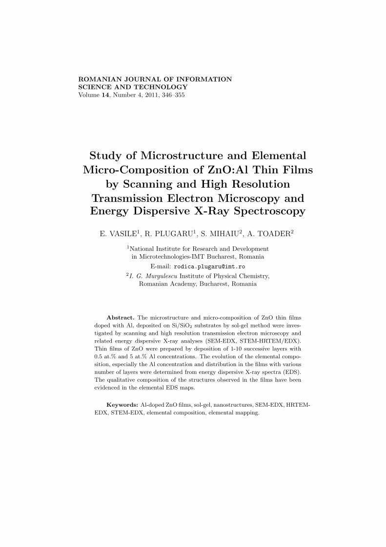
SEM images of ZnO: 5% at. Al doped films with 5 and 10 layers are shown inFigs. 1 (a) and (b). The films present nanograins with the size varying between 8.5–22 nm. We previously reported that the ZnO:Al doped films with wurtzite structureand preferential (002) orientation were obtained by sol-gel deposition on Si/SiO2
substrates [11].
a) b)
Fig. 1. SEM images of the ZnO:5% at. Al doped films with 5 layers (a) and 10 layers (b).
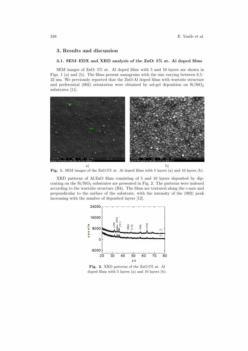
XRD patterns of Al:ZnO films consisting of 5 and 10 layers deposited by dip-coating on the Si/SiO2 substrates are presented in Fig. 2. The patterns were indexedaccording to the wurtzite structure (B4). The films are textured along the c-axis andperpendicular to the surface of the substrate, with the intensity of the (002) peakincreasing with the number of deposited layers [12].
Fig. 2. XRD patterns of the ZnO:5% at. Al
doped films with 5 layers (a) and 10 layers (b).
Microstructure and Elemental Micro-composition of ZnO:Al Thin Films 349
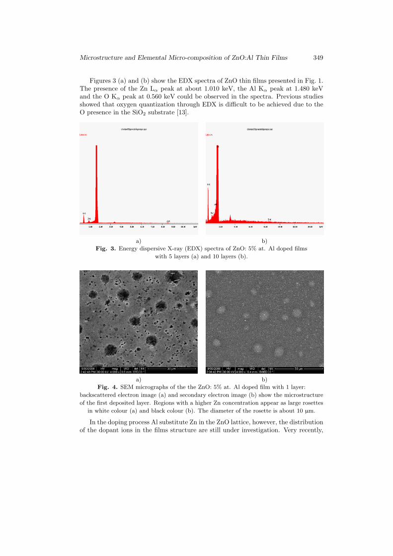
Figures 3 (a) and (b) show the EDX spectra of ZnO thin films presented in Fig. 1.The presence of the Zn Lα peak at about 1.010 keV, the Al Kα peak at 1.480 keVand the O Kα peak at 0.560 keV could be observed in the spectra. Previous studiesshowed that oxygen quantization through EDX is difficult to be achieved due to theO presence in the SiO2 substrate [13].
a) b)
Fig. 3. Energy dispersive X-ray (EDX) spectra of ZnO: 5% at. Al doped films
with 5 layers (a) and 10 layers (b).
a) b)
Fig. 4. SEM micrographs of the the ZnO: 5% at. Al doped film with 1 layer:
backscattered electron image (a) and secondary electron image (b) show the microstructure
of the first deposited layer. Regions with a higher Zn concentration appear as large rosettes
in white colour (a) and black colour (b). The diameter of the rosette is about 10 µm.
In the doping process Al substitute Zn in the ZnO lattice, however, the distributionof the dopant ions in the films structure are still under investigation. Very recently,
350 E. Vasile et al.
TEM investigation of ZnO: 2% at. Al doped polycrystalline films revealed a columnarstructure of the grains and the presence of voids in the grain boundaries region.However, the Al, O, and Zn maps show a homogeneous elements distribution in thefilms [14].
In our study, the early stage of the films deposition was observed in the SEMimages obtained using both BSED (Backscattered Electron Detector) and ETD (sec-ondary electron detector) mode of SEM. The images are presented in Figs. 4 (a) and(b). Regions with a diameter of about 30 µm appear as white dots in BSED imagefrom Fig. 4 (a) and with black contrast in the EDT image from Fig. 4 (b).
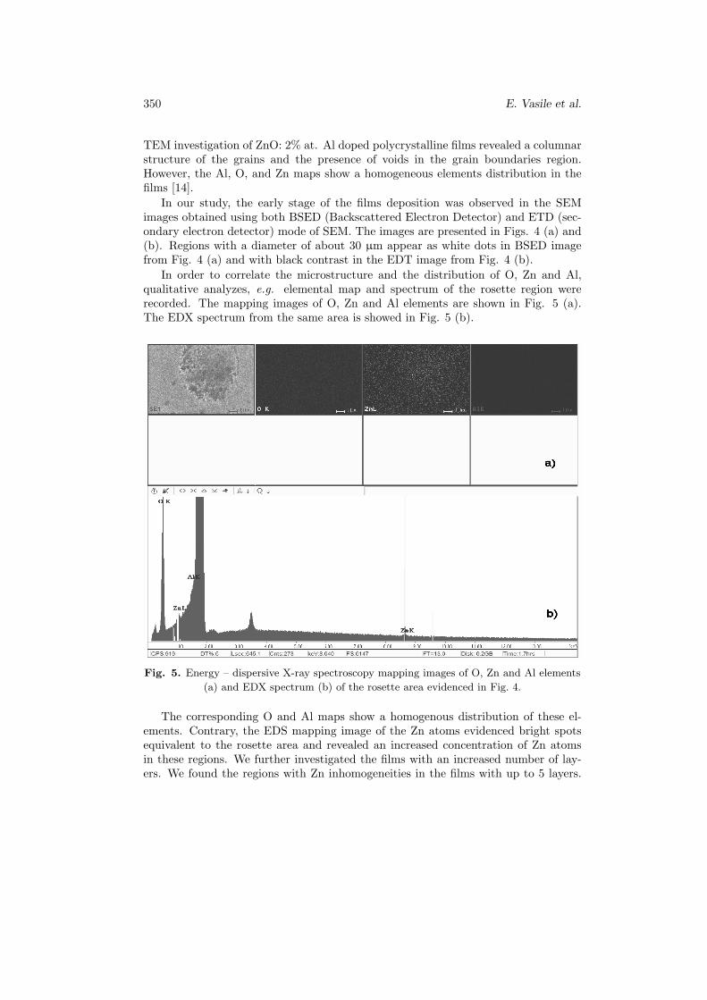
In order to correlate the microstructure and the distribution of O, Zn and Al,qualitative analyzes, e.g. elemental map and spectrum of the rosette region wererecorded. The mapping images of O, Zn and Al elements are shown in Fig. 5 (a).The EDX spectrum from the same area is showed in Fig. 5 (b).
Fig. 5. Energy – dispersive X-ray spectroscopy mapping images of O, Zn and Al elements
(a) and EDX spectrum (b) of the rosette area evidenced in Fig. 4.
The corresponding O and Al maps show a homogenous distribution of these el-ements. Contrary, the EDS mapping image of the Zn atoms evidenced bright spotsequivalent to the rosette area and revealed an increased concentration of Zn atomsin these regions. We further investigated the films with an increased number of lay-ers. We found the regions with Zn inhomogeneities in the films with up to 5 layers.

Microstructure and Elemental Micro-composition of ZnO:Al Thin Films 351
These regions diminished in the films with 6 to 10 layers, where Zn atoms concentra-tion appears more uniform. SEM-EDX analyzes did not provided edifying results onthe Al distribution due to the substrate influence against the films thickness in thecharacteristic X-rays generation.
3.2. STEM-EDX and HRTEM-EDX analysis of the ZnO:0.5% at.
Al doped films
In order to investigate the nanostructure and the elemental distribution of theZnO:0.5% at. Al doped films, STEM-EDX and HRTEM-EDX analyses of the filmswith 5 and 10 layers were performed on the plan view and cross section samples.
Fig. 6. Cross-section bright-field HRTEM images of ZnO:0.5% at. Al doped film
with 10 layers deposited on Si/SiO2 substrate (a) and selected area diffraction SAED (b).
Figure 6 shows a HRTEM cross section image of the ZnO:0.5% at. Al doped film(Fig. 6 (a)) and the selected aria electron diffraction image (SAED) (Fig. 6 (b)). TheHRTEM image evidenced the presence of nanocrystallites randomly distributed in theZnO film area Fig. 6 (a). The SAED image demonstrates the polycrystalline structureof the film with the indexed rings corresponding to wurtzite structure, according topreviously results of XRD analyses (Fig. 2). The presence of large nanocrystallinegrains, with the diameter of the film thickness, preferentially oriented on c-axis wereobserved in the HRTEM cross section images, Fig. 7.
The concentration of the Al ions in the films and their distribution was recordedboth in the plan view and cross section of the films. Figure 8 (a), (b) presents aSTEM image of the cross section from ZnO:0.5% at. Al film with 10 layers, (Fig. 8(a)) and the EDX spectrum recorded in a point of a selected zone (Fig. 8 (b).
The entire marked area from the Fig. 8 (a) was divided into zones and an EDXspectrum was acquired in each zone. The qualitative and quantitative X-ray micro-analyses and maps of the elements were obtained using the recorded EDX spectra.

352 E. Vasile et al.
The EDS maps of O, Zn, and Al shown in Fig. 9 evidenced a relative uniform dis-tribution of the elements in the film area. The results of quantitative X-ray microand nanoanalyses showed that Al concentration in the films with 5 layers was 0.35 ±0.16 at.%. In the case of the film with 10 layers, Al concentration was 0.62 ± 0.08at.%. The elemental composition of the films is presented in the Table 1 and Table 2.
Fig. 7. Cross-section HRTEM image of ZnO:0.5% at. Al filmwith 10 layers deposited on the Si/SiO2 substrate
showing a nanocrystalline grain c-axis oriented.
Table 1. Elemental composition of the ZnO:0.5% at. Al film with 5 layers
Element Weight % Atomic % Uncert. % Correction k-Factor
O(K) 32.76 66.41 0.76 0.49 2.008
Al(K) 0.31 0.37 0.08 0.92 1.030
Zn(K) 66.92 33.20 0.92 0.99 1.68
Table 2. Elemental composition of the ZnO:0.5% at. Al film with 10 layers
Element Weight % Atomic % Uncert. % Correction k-Factor
O(K) 13.72 38.98 0.21 0.49 2.008
Al(K) 0.37 0.62 0.01 0.92 1.030
Zn(K) 75.51 52.48 0.38 0.99 1.686

Microstructure and Elemental Micro-composition of ZnO:Al Thin Films 353
a) b)
Fig. 8. (a) Scanning TEM (STEM) image of cross section sample from ZnO:0.5% at. Al
doped film with 10 layers; (b) EDX spectrum recorded in the marked point from image (a).
Fig. 9. Cross section STEM image of the ZnO:0.5%at. Al film with 10 layers
on the Si/SiO2 substrate and EDS mapping images of O, Zn, Al.

354 E. Vasile et al.
4. Conclusions
Micro-nanostructural and elements composition analyzes of ZnO:5% at. Al andZnO:0.5% at. Al have been performed by SEM-EDX and HRTEM-EDX, STEMmethods. The EDX spectra and elemental mapping evidenced that Zn distributionin the ZnO:5% at Al doped films is not uniform. An increased Al concentration inrandomly distributed areas with about 10 µm diameter was observed in the films withup to 5 layers. A more uniform distribution of Zn was observed in the films with 5 to10 layers. The concentration of Al in the films varied close to the doping values.
Acknowledgments. One of the authors, E. Vasile, acknowledges the support ofthe Project POSDRU/89/1.5/S/63700, 2010-2013.
References
[1] Schuler T., Krajewski T., Grobelsek I., Aegerter M. A., A MicrostructuralZone Model for the Morphology of Sol-Gel Coatings, Journal of Sol-Gel Science andTechnology, Vol. 31, pp. 235–239, 2004.
[2] Kim J., Yun J.-H.,. Jee S.-W, Park Y. C., Ju M., Han S., Kim Y., Kim J.-H.,Anderson W. A., Lee J.-H., Yi J., Rapid thermal annealed Al-doped ZnO film for aUV detector, Materials Letters, Vol. 65, pp. 786–789, 2011.
[3] Gong L., Ye Z., Lu J., Zhu L., Huang J., Gu X., Zhao B., Highly transparentconductive and near-infrared reflective ZnO:Al thin films, Vacuum, Vol. 84, pp. 947–952, 2010.
[4] Chandramohan R., Vijayan T. A., Arumugam S., Ramalingam H. B.,Dhanasekaran V., Sundaram K., Mahalingam T., Effect of heat treatment onmicrostructural and optical properties of CBD grown Al-doped ZnO thin films, Mat.Sci.Eng. B, Vol. 176, pp. 152–156, 2011.
[5] Wang H., Xu M.-Hui, Xu J.-Wen, Ren M.-Fang, Yang L., Low temperature syn-thesis of sol–gel derived Al-doped ZnO thin films with rapid thermal annealing process,J. Mater. Sci.: Mater. Electron., Vol. 21, pp. 589–594, 2010.
[6] Lin K.-Moh, Chen Y.-Y., Chou K.-Y., Solution derived Al-doped zinc oxide films:doping effect, microstructure and electrical property, J. Sol-Gel Sci. Technol., Vol. 49,pp. 238–242, 2009.
[7] Major C., Nemeth A., Radnoczi G., Czigany Zs., Fried M., Labadi Z., Bar-sony I., Optical and electrical characterization of aluminium doped ZnO layers, AppliedSurface Science, Vol. 255, pp. 8907–8912, 2009.
[8] Chen K. J., Fang T. H., Hung F. Y., Ji L. W., Chang S. J., Young S. J., Hsiao Y.J., The crystallization and physical properties of Al-doped ZnO nanoparticles, AppliedSurface Science, Vol. 254, pp. 5791–5795, 2008.
[9] Lin K.-Moh, Chen Y.-Y., Chou K.-Y., Solution derived Al-doped zinc oxide films:doping effect, microstructure and electrical property, J. Sol-Gel Sci. Technol., Vol. 49,pp. 238–242, 2009.
[10] Han J. H., No Y. S., Kim T. W., Lee J. Y., Kim J. Y., Choi W. K., Microstruc-tural and surface property variations due to the amorphous region formed by thermal

Microstructure and Elemental Micro-composition of ZnO:Al Thin Films 355
annealing in Al-doped ZnO thin films grown on n-Si (1 0 0) substrates, App. Surf. Sci.,Vol. 256, pp. 1920–1924, 2010.
[11] Mihaiu S., Toader A., Atkinson I., Anastasescu M., Vasilescu M., ZaharescuM., Plugaru R., Al–doped ZnO nanocoatings obtained by sol-gel route, ProceedingsSPIE Advances Topics in Optoelectronics, microelectronics and nanotechnologies V,Vol. 7821, p. 78211D, 2010.
[12] Plugaru R., Plugaru N., Mihaiu S., Vasile E., On the electrical conductivity inAl:ZnO layers; experimental investigation and a theoretical approach, Internat. Semic.Conf. Proceedings CAS 2010, pp. 345–348, 2010.
[13] Fragala M. E., Malandrino G., Characterization of ZnO and ZnO:Al films depositedby MOCVD on oriented and amorphous substrates, Microelectronics Journal, Vol. 40,pp. 381–384, 2009.
[14] Major C., Nemeth A., Radnoczi G., Czigany Zs., Fried M., Labadi Z., BarsonyI., Optical and electrical characterization of aluminium doped ZnO layers, App. Surf.Sci., Vol. 255, pp. 8907–8912, 2009.