Signal and Power Isolated CAN Transceiver with … and Power Isolated CAN Transceiver with...
18
Signal and Power Isolated CAN Transceiver with Integrated Isolated DC-to-DC Converter Data Sheet ADM3053 Rev. E Document Feedback Information furnished by Analog Devices is believed to be accurate and reliable. However, no responsibility is assumed by Analog Devices for its use, nor for any infringements of patents or other rights of third parties that may result from its use. Specifications subject to change without notice. No license is granted by implication or otherwise under any patent or patent rights of Analog Devices. Trademarks and registered trademarks are the property of their respective owners. One Technology Way, P.O. Box 9106, Norwood, MA 02062-9106, U.S.A. Tel: 781.329.4700 ©2011–2017 Analog Devices, Inc. All rights reserved. Technical Support www.analog.com FEATURES 2.5 kV rms signal and power isolated CAN transceiver isoPower integrated isolated dc-to-dc converter 5 V operation on VCC 5 V or 3.3 V operation on VIO Complies with ISO 11898 standard High speed data rates of up to 1 Mbps Unpowered nodes do not disturb the bus Connect 110 or more nodes on the bus Slope control for reduced EMI Thermal shutdown protection High common-mode transient immunity: >25 kV/μs Safety and regulatory approvals UL recognition 2500 V rms for 1 minute per UL 1577 CSA Component Acceptance Notice 5A VDE Certificate of Conformity DIN EN 60747-5-2 (VDE 0884 Part 2): 2003-01 VIORM = 560 V peak Industrial operating temperature range (−40°C to +85°C) Available in wide-body, 20-lead SOIC package APPLICATIONS CAN data buses Industrial field networks GENERAL DESCRIPTION The ADM3053 is an isolated controller area network (CAN) physical layer transceiver with an integrated isolated dc-to-dc converter. The ADM3053 complies with the ISO 11898 standard. The device employs Analog Devices, Inc., iCoupler® technology to combine a 2-channel isolator, a CAN transceiver, and Analog Devices isoPower® dc-to-dc converter into a single SOIC surface mount package. An on-chip oscillator outputs a pair of square waveforms that drive an internal transformer to provide isolated power. The device is powered by a single 5 V supply realizing a fully isolated CAN solution. The ADM3053 creates a fully isolated interface between the CAN protocol controller and the physical layer bus. It is capable of running at data rates of up to 1 Mbps. The device has current limiting and thermal shutdown features to protect against output short circuits. The part is fully specified over the industrial temperature range and is available in a 20-lead, wide-body SOIC package. The ADM3053 contains isoPower technology that uses high frequency switching elements to transfer power through the transformer. Special care must be taken during printed circuit board (PCB) layout to meet emissions standards. Refer to the AN-0971 Application Note, Recommendations for Control of Radiated Emissions with isoPower Devices, for details on board layout considerations. FUNCTIONAL BLOCK DIAGRAM ADM3053 TxD V CC RxD ISOLATION BARRIER LOGIC SIDE BUS SIDE ENCODE DECODE DECODE ENCODE OSCILLATOR RECTIFIER REGULATOR DIGITAL ISOLATION iCoupler isoPower DC-TO-DC CONVERTER V IO V ISOIN V ISOOUT R S CANH CANL V REF REFERENCE VOLTAGE RECEIVER CAN TRANSCEIVER TxD R S RxD V REF GND2 V CC SLOPE/ STANDBY DRIVER PROTECTION 09293-001 GND1 GND2 PIN 11, PIN 13 GND2 PIN 16, PIN 20 Figure 1.
Transcript of Signal and Power Isolated CAN Transceiver with … and Power Isolated CAN Transceiver with...
Signal and Power Isolated CAN Transceiver with Integrated Isolated DC-to-DC Converter
Data Sheet ADM3053
Rev. E Document Feedback Information furnished by Analog Devices is believed to be accurate and reliable. However, no responsibility is assumed by Analog Devices for its use, nor for any infringements of patents or other rights of third parties that may result from its use. Specifications subject to change without notice. No license is granted by implication or otherwise under any patent or patent rights of Analog Devices. Trademarks and registered trademarks are the property of their respective owners.
One Technology Way, P.O. Box 9106, Norwood, MA 02062-9106, U.S.A.Tel: 781.329.4700 ©2011–2017 Analog Devices, Inc. All rights reserved. Technical Support www.analog.com
FEATURES 2.5 kV rms signal and power isolated CAN transceiver isoPower integrated isolated dc-to-dc converter 5 V operation on VCC 5 V or 3.3 V operation on VIO Complies with ISO 11898 standard High speed data rates of up to 1 Mbps Unpowered nodes do not disturb the bus Connect 110 or more nodes on the bus Slope control for reduced EMI Thermal shutdown protection High common-mode transient immunity: >25 kV/μs Safety and regulatory approvals
UL recognition 2500 V rms for 1 minute per UL 1577
CSA Component Acceptance Notice 5A VDE Certificate of Conformity DIN EN 60747-5-2 (VDE 0884 Part 2): 2003-01
VIORM = 560 V peak Industrial operating temperature range (−40°C to +85°C) Available in wide-body, 20-lead SOIC package
APPLICATIONS CAN data buses Industrial field networks
GENERAL DESCRIPTION The ADM3053 is an isolated controller area network (CAN) physical layer transceiver with an integrated isolated dc-to-dc converter. The ADM3053 complies with the ISO 11898 standard.
The device employs Analog Devices, Inc., iCoupler® technology to combine a 2-channel isolator, a CAN transceiver, and Analog Devices isoPower® dc-to-dc converter into a single SOIC surface mount package. An on-chip oscillator outputs a pair of square waveforms that drive an internal transformer to provide isolated power. The device is powered by a single 5 V supply realizing a fully isolated CAN solution.
The ADM3053 creates a fully isolated interface between the CAN protocol controller and the physical layer bus. It is capable of running at data rates of up to 1 Mbps.
The device has current limiting and thermal shutdown features to protect against output short circuits. The part is fully specified over the industrial temperature range and is available in a 20-lead, wide-body SOIC package.
The ADM3053 contains isoPower technology that uses high frequency switching elements to transfer power through the transformer. Special care must be taken during printed circuit board (PCB) layout to meet emissions standards. Refer to the AN-0971 Application Note, Recommendations for Control of Radiated Emissions with isoPower Devices, for details on board layout considerations.
FUNCTIONAL BLOCK DIAGRAM
ADM3053
TxD
VCC
RxD
ISOLATIONBARRIER
LOGIC SIDE BUS SIDE
ENCODE
DECODE
DECODE
ENCODE
OSCILLATOR RECTIFIER
REGULATOR
DIGITAL ISOLATION iCoupler
isoPower DC-TO-DC CONVERTER
VIO
VISOIN
VISOOUT
RS
CANH
CANL
VREF
REFERENCEVOLTAGE
RECEIVER
CAN TRANSCEIVER
TxD
RS
RxD
VREF
GND2
VCC
SLOPE/STANDBY
DRIVER
PROTECTION
092
93-
001GND1 GND2
PIN 11, PIN 13GND2PIN 16, PIN 20
Figure 1.

ADM3053 Data Sheet
Rev. E | Page 2 of 18
TABLE OF CONTENTS Features .............................................................................................. 1 Applications ....................................................................................... 1 General Description ......................................................................... 1 Functional Block Diagram .............................................................. 1 Revision History ............................................................................... 2 Specifications ..................................................................................... 3
Timing Specifications .................................................................. 4 Switching Characteristics ............................................................ 4 Regulatory Information ............................................................... 5 Insulation and Safety-Related Specifications ............................ 5 VDE 0884 Insulation Characteristics ........................................ 6
Absolute Maximum Ratings ............................................................ 7 ESD Caution .................................................................................. 7
Pin Configuration and Function Descriptions ............................. 8 Typical Performance Characteristics ............................................. 9 Test Circuits ..................................................................................... 12
Circuit Description......................................................................... 13 CAN Transceiver Operation ..................................................... 13 Signal Isolation ........................................................................... 13 Power Isolation ........................................................................... 13 Truth Tables................................................................................. 13 Thermal Shutdown .................................................................... 13 DC Correctness and Magnetic Field Immunity ........................... 14
Applications Information .............................................................. 15 PCB Layout ................................................................................. 15 EMI Considerations ................................................................... 15 RS Pin ............................................................................................ 16 Insulation Lifetime ..................................................................... 16
Typical Applications ....................................................................... 17 Outline Dimensions ....................................................................... 18
Ordering Guide .......................................................................... 18
REVISION HISTORY 12/2017—Rev. D to Rev. E Changes to Logic Side isoPower Current, Dominant State Parameter and TxD/RxD Data Rate 1 Mbps Parameter, Table 1 ................................................................................................ 3 Moved Figure 3 ................................................................................. 4 Change to TJ Junction Temperature, Table 6 ................................ 7 Changes to Figure 28 ...................................................................... 15 7/2017—Rev. C to Rev. D Moved Figure 1 ................................................................................. 3 Changes to Figure 1 .......................................................................... 3 Change to Tracking Resistance (Comparative Tracking Index) Parameter, Table 4 ................................................................ 6 Changes to Table 8 ............................................................................ 9 Changes to Power Isolation Section ............................................. 14 Changes to PCB Layout Section and Figure 28 .......................... 16 Added RS Pin Section ..................................................................... 17 Changes to Figure 32 ...................................................................... 18
11/2016—Rev. B to Rev. C Change to Table 4 .............................................................................. 5 Changes to Figure 11 Caption ...................................................... 10 Changes to Ordering Guide .......................................................... 18 2/2013—Rev. A to Rev. B Changes to Features Section ............................................................ 1 Changes to Table 3 ............................................................................. 5 Changes to Table 7 ............................................................................. 7 3/2012—Rev. 0 to Rev. A Changes to Features Section ............................................................ 1 Changes to Table 3 ............................................................................. 5 Changes to VDE 0884 Insulation Characteristics Section ........... 6 Changes to Figure 6 ........................................................................... 9 Changes to Figure 11 ...................................................................... 10 Changes to Applications Information Section ........................... 15 5/2011—Revision 0: Initial Version

Data Sheet ADM3053
Rev. E | Page 3 of 18
SPECIFICATIONS All voltages are relative to their respective grounds; 4.5 V ≤ VCC ≤ 5.5 V; 3.0 V ≤ VIO ≤ 5.5 V. All minimum/maximum specifications apply over the entire recommended operation range, unless otherwise noted. All typical specifications are at TA = 25°C, VCC = 5 V, and VIO = 5 V unless otherwise noted.
Table 1. Parameter Symbol Min Typ Max Unit Test Conditions/Comments SUPPLY CURRENT
Logic Side isoPower Current Recessive State ICC 29 36 mA RL = 60 Ω, RS = low, see Figure 25 Dominant State ICC 195 260 mA RL = 60 Ω, RS = low, see Figure 25 TxD/RxD Data Rate 1 Mbps ICC 139 200 mA RL = 60 Ω, RS = low, see Figure 25
Logic Side iCoupler Current TxD/RxD Data Rate 1 Mbps IIO 1.6 2.5 mA
DRIVER Logic Inputs
Input Voltage High VIH 0.7 VIO V Output recessive Input Voltage Low VIL 0.25 VIO V Output dominant CMOS Logic Input Currents IIH, IIL 500 µA TxD
Differential Outputs Recessive Bus Voltage VCANL, VCANH 2.0 3.0 V TxD = high, RL = ∞, see Figure 22 CANH Output Voltage VCANH 2.75 4.5 V TxD = low, see Figure 22 CANL Output Voltage VCANL 0.5 2.0 V TxD = low, see Figure 22 Differential Output Voltage VOD 1.5 3.0 V TxD = low, RL = 45 Ω, see Figure 22
VOD −500 +50 mV TxD = high, RL = ∞, see Figure 22
Short-Circuit Current, CANH ISCCANH −200 mA VCANH = −5 V −100 mA VCANH = −36 V Short-Circuit Current, CANL ISCCANL 200 mA VCANL = 36 V
RECEIVER Differential Inputs
Differential Input Voltage Recessive VIDR −1.0 +0.5 V −7 V < VCANL, VCANH < +12 V, see Figure 23, CL = 15 pF
Differential Input Voltage Dominant VIDD 0.9 5.0 V −7 V < VCANL, VCANH < +12 V, see Figure 23, CL = 15 pF
Input Voltage Hysteresis VHYS 150 mV See Figure 3 CANH, CANL Input Resistance RIN 5 25 kΩ Differential Input Resistance RDIFF 20 100 kΩ
Logic Outputs Output Low Voltage VOL 0.2 0.4 V IOUT = 1.5 mA
Output High Voltage VOH VIO − 0.3 VIO − 0.2 V IOUT = −1.5 mA
Short Circuit Current IOS 7 85 mA VOUT = GND1 or VIO VOLTAGE REFERENCE
Reference Output Voltage VREF 2.025 3.025 V |IREF = 50 µA| COMMON-MODE TRANSIENT IMMUNITY1 25 kV/µs VCM = 1 kV, transient magnitude = 800 V SLOPE CONTROL
Current for Slope Control Mode ISLOPE −10 −200 µA Slope Control Mode Voltage VSLOPE 1.8 3.3 V
1 CM is the maximum common-mode voltage slew rate that can be sustained while maintaining specification compliant operation. VCM is the common-mode potential
difference between the logic and bus sides. The transient magnitude is the range over which the common mode is slewed. The common-mode voltage slew rates apply to both rising and falling common-mode voltage edges.

ADM3053 Data Sheet
Rev. E | Page 4 of 18
TIMING SPECIFICATIONS All voltages are relative to their respective ground; 3.0 V ≤ VIO ≤ 5.5 V; 4.5 V ≤ VCC ≤ 5.5 V. TA = −40°C to +85°C, unless otherwise noted.
Table 2. Parameter Symbol Min Typ Max Unit Test Conditions/Comments DRIVER
Maximum Data Rate 1 Mbps Propagation Delay from TxD On to Bus Active tonTxD 90 ns RS = 0 Ω; see Figure 2 and Figure 24
RL = 60 Ω, CL = 100 pF Propagation Delay from TxD Off to Bus Inactive toffTxD 120 ns RS = 0 Ω; see Figure 2 and Figure 24
RL = 60 Ω, CL = 100 pF RECEIVER
Propagation Delay from TxD On to Receiver Active tonRxD 200 ns RS = 0 Ω; see Figure 2 630 ns RS = 47 kΩ; see Figure 2 Propagation Delay from TxD Off to Receiver Inactive1 toffRxD 250 ns RS = 0 Ω; see Figure 2 480 ns RS = 47 kΩ; see Figure 2
CANH, CANL SLEW RATE |SR| 7 V/µs RS = 47 kΩ 1 Guaranteed by design and characterization.
SWITCHING CHARACTERISTICS
0.25VIO
0.9V
VOR
VOD
0V
0V
VIO
0.5V
0.4V
VDIFF
VRxD
VIO
VTxD
VIO – 0.3V
0.7VIO
VDIFF = VCANH – VCANL
tonTxD toffTxD
tonRxD toffRxD
0929
3-00
2
Figure 2. Driver Propagation Delay, Rise/Fall Timing
0.5 0.9
VRxD
HIGH
LOWVHYS
VID (V)
0929
3-00
4
Figure 3. Receiver Input Hysteresis

Data Sheet ADM3053
Rev. E | Page 5 of 18
REGULATORY INFORMATION
Table 3. ADM3053 Approvals Organization Approval Type Notes UL Recognized under the Component Recognition
Program of Underwriters Laboratories, Inc. In accordance with UL 1577, each ADM3053 is proof tested by applying an insulation test voltage ≥2500 V rms for 1 second. File E214100.
VDE Certified according to DIN EN 60747-5-2 (VDE 0884 Part 2): 2003-01.
In accordance with VDE 0884-2. File 2471900-4880-0001.
CSA Approved under CSA Component Acceptance Notice 5A. Testing was conducted per CSA 60950-1-07 and IEC 60950-1, 2nd Edition at 2.5 kV rated voltage. Testing was conducted per CSA 61010-1-04 and IEC 61010-1 2nd Edition at 2.5 kV rated voltage.
Basic insulation at 760 V rms (1074 V peak) working voltage. Reinforced insulation at 380 V rms (537 V peak) working voltage. Basic insulation at 424 V rms (600 V peak) working voltage. Reinforced insulation at 300 V rms (424 V peak) working voltage. File 205078.
INSULATION AND SAFETY-RELATED SPECIFICATIONS
Table 4. Parameter Symbol Value Unit Test Conditions/Comments Rated Dielectric Insulation Voltage 2500 V rms 1-minute duration Minimum External Air Gap (Clearance) L(I01) 7.7 mm Measured from input terminals to output terminals,
shortest distance through air Minimum External Tracking (Creepage) L(I02) 7.6 mm Measured from input terminals to output terminals,
shortest distance along body Minimum Internal Gap (Internal
Clearance) 0.017 min mm Insulation distance through insulation
Tracking Resistance (Comparative Tracking Index)
CTI >400 V DIN IEC 112/VDE 0303-1
Isolation Group II Material group (DIN VDE 0110: 1989-01, Table 1)

ADM3053 Data Sheet
Rev. E | Page 6 of 18
VDE 0884 INSULATION CHARACTERISTICS This isolator is suitable for basic electrical isolation only within the safety limit data. Maintenance of the safety data must be ensured by means of protective circuits.
Table 5. Description Test Conditions/Comments Symbol Characteristic Unit CLASSIFICATIONS
Installation Classification per DIN VDE 0110 for Rated Mains Voltage
≤150 V rms I to IV ≤300 V rms I to III ≤400 V rms I to II
Climatic Classification 40/85/21 Pollution Degree DIN VDE 0110, see Table 3 2
VOLTAGE Maximum Working Insulation Voltage VIORM 560 VPEAK Input-to-Output Test Voltage VPR
Method b1 VIORM × 1.875 = VPR, 100% production tested, tm = 1 sec, partial discharge < 5 pC
1050 VPEAK
Highest Allowable Overvoltage (Transient overvoltage, tTR = 10 sec) VTR 4000 VPEAK SAFETY-LIMITING VALUES Maximum value allowed in the event of a
failure
Case Temperature TS 150 °C Input Current IS, INPUT 265 mA Output Current IS, OUTPUT 335 mA Insulation Resistance at TS VIO = 500 V RS >109 Ω

Data Sheet ADM3053
Rev. E | Page 7 of 18
ABSOLUTE MAXIMUM RATINGS TA = 25°C, unless otherwise noted. All voltages are relative to their respective ground.
Table 6. Parameter Rating VCC −0.5 V to +6 V VIO −0.5 V to +6 V Digital Input Voltage, TxD −0.5 V to VIO + 0.5 V Digital Output Voltage, RxD −0.5 V to VIO + 0.5 V CANH, CANL −36 V to +36 V VREF −0.5 V to +6 V RS −0.5 V to +6 V Operating Temperature Range −40°C to +85°C Storage Temperature Range −55°C to +150°C
ESD (Human Body Model) 3 kV
Lead Temperature Soldering (10 sec) 300°C Vapor Phase (60 sec) 215°C Infrared (15 sec) 220°C
θJA Thermal Impedance 53°C/W TJ Junction Temperature 150°C
Stresses at or above those listed under Absolute Maximum Ratings may cause permanent damage to the product. This is a stress rating only; functional operation of the product at these or any other conditions above those indicated in the operational section of this specification is not implied. Operation beyond the maximum operating conditions for extended periods may affect product reliability.
Table 7. Maximum Continuous Working Voltage1 Parameter Max Unit Reference Standard AC Voltage
Bipolar Waveform 424 V peak 50 year minimum lifetime
Unipolar Waveform Basic Insulation 1074 V peak Maximum approved
working voltage per IEC60950-1
Reinforced Insulation 537 V peak Maximum approved working voltage per IEC60950-1
DC Voltage
Basic Insulation 1074 V peak Maximum approved working voltage per IEC60950-1
Reinforced Insulation 537 V peak Maximum approved working voltage per IEC60950-1
1 Refers to continuous voltage magnitude imposed across the isolation
barrier. See the Insulation Lifetime section for more details.
ESD CAUTION

ADM3053 Data Sheet
Rev. E | Page 8 of 18
PIN CONFIGURATION AND FUNCTION DESCRIPTIONS GND1 1
NC 2
GND1 3
RxD 4
GND220
VISOIN19
RS18
CANH17
TxD 5 GND216
VIO 6 CANL15
GND1 7 VREF14
VCC 8 GND213
GND1 9 VISOOUT12
GND1 10 GND211
ADM3053TOP VIEW
(Not to Scale)
NOTES1. NC = NO CONNECT. DO NOT
CONNECT TO THIS PIN.2. PIN 12 AND PIN 19 MUST BE
CONNECTED EXTERNALLY. 0929
3-00
5
Figure 4. Pin Configuration
Table 8. Pin Function Descriptions Pin No. Mnemonic Description 1, 3, 7, 9, 10 GND1 Ground, Logic Side. 2 NC No Connect. Do not connect to this pin. 4 RxD Receiver Output Data. 5 TxD Driver Input Data. 6 VIO iCoupler Power Supply. It is recommended that a 0.1 μF and a 0.01 μF decoupling capacitor be fitted
between Pin 6 and GND1. See Figure 28 for layout recommendations. 8 VCC isoPower Power Supply. It is recommended that a 0.1 μF and a 10 μF decoupling capacitor be fitted
between Pin 8 and Pin 9. 11, 13 GND2 Ground for Isolated DC-to-DC Converter. It is recommended to connect Pin 11 and Pin 13 together through
one ferrite bead to the PCB ground. 12 VISOOUT Isolated Power Supply Output. This pin must be connected externally to VISOIN. It is recommended that a ferrite
bead reservoir capacitor of 10 μF and a decoupling capacitor of 0.1 μF be fitted between Pin 12 and Pin 11. 14 VREF Reference Voltage Output. It is recommended not to connect to this pin. 15 CANL Low-Level CAN Voltage Input/Output. 16, 20 GND2 Ground, Bus Side. 17 CANH High-Level CAN Voltage Input/Output. 18 RS Slope Control Pin. Short this pin to GND2 (Pin 16 or Pin 20) for full speed operation. Use a weak pull-down for
slope control. An input high places the transceiver in standby. This pin must not be left floating. 19 VISOIN Isolated Power Supply Input. This pin must be connected externally to VISOOUT. It is recommended this pin
have a 0.1 μF capacitor to GND2 (Pin13 or Pin 11). Connect this pin through a ferrite bead and short trace length to VISOIN for operation.

Data Sheet ADM3053
Rev. E | Page 9 of 18
TYPICAL PERFORMANCE CHARACTERISTICS 160
0
20
40
60
80
100
120
140
100 1000
SUPP
LY C
UR
REN
T, I C
C (m
A)
DATA RATE (kbps)
VCC = 4.5V, VIO = 5V
VCC = 5.5V, VIO = 5V
VCC = 5V, VIO = 5V
0929
3-10
0
Figure 5. Supply Current, ICC vs. Data Rate
50
45
40
35
30
25
20
15
10
5
00 10 20 30 40 50 60 70 80
SLEW
RA
TE (V
/µs)
RESISTANCE, RS (kΩ)
0929
3-10
1
Figure 6. Driver Slew Rate vs. Resistance, RS
5.5
4.5
3.5
2.5
1.5
0.5100 1000
SUPP
LY C
UR
REN
T, I I
O (m
A)
DATA RATE (kbps)
VIO = 3.3V
VIO = 5V
0929
3-10
2
Figure 7. Supply Current, IIO vs. Data Rate
180
175
170
165
160
155
150–40 85603510–15
RECE
IVER
INPU
T HY
STER
ESIS
(mV)
TEMPERATURE (°C)
VCC = 5V, VIO = 5V
VCC = 5V, VIO = 3.3V
0929
3-10
3
Figure 8. Receiver Input Hysteresis vs. Temperature
53
52
51
50
49
48
47–40 85603510–15
PRO
PAG
ATI
ON
DEL
AY
TxD
ON
TO
BU
S A
CTI
VE,
t onT
xD (n
s)
TEMPERATURE (°C)
VCC = 5V, VIO = 5V
VCC = 5V, VIO = 3.3V
0929
3-10
4
Figure 9. Propagation Delay from TxD On to Bus Active vs. Temperature
96
94
92
90
88
86
84
82
80
78–40 85603510–15
PRO
PAG
ATI
ON
DEL
AY
TxD
OFF
TO
BU
SIN
AC
TIVE
,tof
fTxD
(ns)
TEMPERATURE (°C)
VCC = 5V, VIO = 5V
VCC = 5V, VIO = 3.3V
0929
3-10
5
Figure 10. Propagation Delay from TxD Off to Bus Inactive vs. Temperature

ADM3053 Data Sheet
Rev. E | Page 10 of 18
152
150
148
146
144
142
140
138
136
134–40 85603510–15
PRO
PAG
ATI
ON
DEL
AY
TxD
ON
TO
REC
EIVE
RA
CTI
VE, t
onR
xD (n
s)
TEMPERATURE (°C)
VCC = 5V, VIO = 5V, RS = 0Ω
VCC = 5V, VIO = 3.3V, RS = 0Ω
0929
3-10
6
Figure 11. Propagation Delay from TxD On to Receiver Active vs.
Temperature
600
500
400
300
200
100
0–40 85603510–15
PRO
PAG
ATI
ON
DEL
AY
TxD
ON
TO
REC
EIVE
RA
CTI
VE,t
onR
xD (n
s)
TEMPERATURE (°C)
VCC = 5V, VIO = 5V, RS = 47kΩ
VCC = 5V, VIO = 3.3V, RS = 47kΩ
0929
3-10
7
Figure 12. Propagation Delay from TxD On to Receiver Active vs.
Temperature
250
200
150
100
50
0–40 85603510–15
PRO
PAG
ATI
ON
DEL
AY
TxD
OFF
TO
REC
EIVE
RIN
AC
TIVE
,tof
fRxD
(ns)
TEMPERATURE (°C)
VCC = 5V, VIO = 5V, RS = 0Ω
VCC = 5V, VIO = 3.3V, RS = 0Ω
0929
3-10
8
Figure 13. Propagation Delay from TxD Off to Receiver Inactive vs.
Temperature
330
325
320
315
310
305
300
295
290
285
280
275–40 85603510–15
PRO
PAG
ATI
ON
DEL
AY
TxD
OFF
TO
REC
EIVE
RIN
AC
TIVE
, tof
fRxD
(ns)
TEMPERATURE (°C)
VCC = 5V, VIO = 5V, RS = 47kΩ
VCC = 5V, VIO = 3.3V, RS = 47kΩ
0929
3-10
9
Figure 14. Propagation Delay from TxD Off to Receiver Inactive vs.
Temperature
2.55
2.50
2.45
2.40
2.35
2.30
2.25–40 85603510–15
DIF
FER
ENTI
AL
OU
TPU
T VO
LTA
GE
DO
MIN
AN
T,V O
D (V
)
TEMPERATURE (°C)
VCC = 5V, VIO = 5V, RL = 60ΩVCC = 5V, VIO = 3.3V, RL = 60ΩVCC = 5V, VIO = 5V, RL = 45ΩVCC = 5V, VIO = 3.3V, RL = 45Ω
0929
3-11
0
Figure 15. Differential Output Voltage Dominant vs. Temperature
2.55
2.50
2.45
2.40
2.35
2.30
2.254.5 5.55.35.14.94.7
DIF
FER
ENTI
AL
OU
TPU
T VO
LTA
GE
DO
MIN
AN
T,V O
D (V
)
SUPPLY VOLTAGE, VCC (V)
VIO = 5V, TA = 25°C, RL = 60Ω
VIO = 5V, TA = 25°C, RL = 45Ω
0929
3-11
1
Figure 16. Differential Output Voltage Dominant vs. Supply Voltage, VCC

Data Sheet ADM3053
Rev. E | Page 11 of 18
2.80
2.75
2.70
2.65
2.60
2.55
2.50
2.45
2.40–40 85603510–15
REF
EREN
CE
VOLT
AG
E, V
REF
(V)
TEMPERATURE (°C)
VCC = 5V, VIO = 5V, IREF = +50µA
VCC = 5V, VIO = 5V, IREF = –50µA
VCC = 5V, VIO =5V, IREF = +5µA
VCC = 5V, VIO = 5V, IREF = –5µA
0929
3-11
2
Figure 17. Reference Voltage vs. Temperature
160
140
120
100
80
60
40
20
0–40 85603510–15
SUPP
LY C
UR
REN
T, I C
C (m
A)
TEMPERATURE (°C)
VCC = 5VVIO = 5VDATA RATE = 1MbpsRL = 60Ω
0929
3-11
3
Figure 18. Supply Current ICC vs. Temperature
140
138
136
134
132
130
128
126
124
122
120
1184.5 5.55.45.35.25.15.04.94.84.74.6
SUPP
LY C
UR
REN
T, I C
C (m
A)
SUPPLY VOLTAGE, VCC (V)
VIO = 5VTA = 25°CDATA RATE = 1Mbps
0929
3-11
4
Figure 19. Supply Current, ICC vs. Supply Voltage VCC
–40 85603510–15
REC
EIVE
R O
UTP
UT
HIG
H V
OLT
AG
E, V
OH
(V)
TEMPERATURE (°C)
VCC = 5V, VIO = 5V, IOUT = –1.5mA
4.855
4.860
4.865
4.870
4.875
4.880
4.885
4.890
4.895
0929
3-11
5
Figure 20. Receiver Output High Voltage vs. Temperature
–40 85603510–15
REC
EIVE
R O
UTP
UT
LOW
VO
LTA
GE,
VO
L (m
V)
TEMPERATURE (°C)
0
120
100
80
60
40
20
0929
3-11
6
Figure 21. Receiver Output Low Voltage vs. Temperature
ADM3053 Data Sheet
Rev. E | Page 12 of 18
TEST CIRCUITS
TxD VOD VCANH
VCANH
VOC
RL
RL
2
2
0929
3-00
6
Figure 22. Driver Voltage Measurement
CL
RxD
CANH
CANL
VID
0929
3-00
7
Figure 23. Receiver Voltage Measurements
CANH
CANL
TxD
RxD
CLRL
15pF
092
93-
00
8
Figure 24. Switching Characteristics Measurements
RL
RS
10µF100nF
10µF 100nF
10µF100nF10µF100nF
ADM3053
TxD
RxD
ISOLATIONBARRIER
GND1 GND2
LOGIC SIDE BUS SIDE
ENCODE
DECODE
DECODE
ENCODE
OSCILLATOR RECTIFIER
REGULATOR
VISOOUT
DIGITAL ISOLATION iCoupler
isoPower DC-TO-DC CONVERTER
VIO VISOIN
RS
CANH
CANL
VREF
REFERENCEVOLTAGE
RECEIVER
CAN TRANSCEIVER
TxD
RS
RxD
VREF
GND2
VCC
SLOPE/STANDBY
DRIVER
PROTECTION
VCC
0929
3-0
09
Figure 25. Supply Current Measurement Test Circuit

Data Sheet ADM3053
Rev. E | Page 13 of 18
CIRCUIT DESCRIPTION CAN TRANSCEIVER OPERATION A CAN bus has two states called dominant and recessive. A dominant state is present on the bus when the differential voltage between CANH and CANL is greater than 0.9 V. A recessive state is present on the bus when the differential voltage between CANH and CANL is less than 0.5 V. During a dominant bus state, the CANH pin is high, and the CANL pin is low. During a recessive bus state, both the CANH and CANL pins are in the high impedance state.
Pin 18 (RS) allows two different modes of operation to be selected: high-speed and slope control. For high-speed operation, the transmitter output transistors are simply switched on and off as fast as possible. In this mode, no measures are taken to limit the rise and fall slopes. A shielded cable is recommended to avoid electromagnetic interference (EMI) problems. High-speed mode is selected by connecting Pin 18 to ground.
Slope control mode allows the use of an unshielded twisted pair or a parallel pair of wires as bus lines. To reduce EMI, the rise and fall slopes must be limited. The rise and fall slopes can be programmed with a resistor connected from Pin 18 to ground. The slope is proportional to the current output at Pin 18.
SIGNAL ISOLATION The ADM3053 signal isolation is implemented on the logic side of the interface. The part achieves signal isolation by having a digital isolation section and a transceiver section (see Figure 1). Data applied to the TxD pin referenced to logic ground (GND1) are coupled across an isolation barrier to appear at the transceiver section referenced to isolated ground (GND2). Similarly, the single-ended receiver output signal, referenced to isolated ground in the transceiver section, is coupled across the isolation barrier to appear at the RxD pin referenced to logic ground (GND1). The signal isolation is powered by the VIO pin and allows the digital interface to 3.3 V or 5 V logic.
POWER ISOLATION The ADM3053 power isolation is implemented using an isoPower integrated isolated dc-to-dc converter. The dc-to-dc converter section of the ADM3053 works on principles that are common to most modern power supplies. It is a secondary side controller architecture with isolated pulse-width modulation (PWM) feedback. VCC power is supplied to an oscillating circuit that switches current into a chip-scale air core transformer. Power transferred to the secondary side is rectified and regulated to 5 V. The secondary (VISO) side controller regulates the output by creating a PWM control signal that is sent to the primary (VCC) side by a dedicated iCoupler data channel. The PWM modulates the oscillator circuit to control the power being sent to the secondary side. Feedback allows for significantly higher power and efficiency.
The ADM3053 integrated dc-to-dc converter is designed as a self contained solution and must not drive an external load. To meet additional isolated power needs, isoPower isolated dc-to-dc converters are available in a variety of power or power plus standard data channel options.
TRUTH TABLES The truth tables in this section use the abbreviations found in Table 9.
Table 9. Truth Table Abbreviations Letter Description H High level L Low level X Don’t care Z High impedance (off ) I Indeterminate NC Not connected
Table 10. Transmitting Supply Status Input Outputs VIO VCC TxD Bus State CANH CANL On On L Dominant H L On On H Recessive Z Z On On Floating Recessive Z Z Off On X Recessive Z Z On Off L Indeterminate I I
Table 11. Receiving Supply Status Inputs Output VIO VCC VID = CANH − CANL Bus State RxD On On ≥ 0.9 V Dominant L On On ≤ 0.5 V Recessive H On On 0.5 V < VID < 0.9 V X1 I
On On Inputs open Recessive H Off On X1 X1 I
On Off X1 X1 H 1 X means don’t care.
THERMAL SHUTDOWN The ADM3053 contains thermal shutdown circuitry that protects the part from excessive power dissipation during fault conditions. Shorting the driver outputs to a low impedance source can result in high driver currents. The thermal sensing circuitry detects the increase in die temperature under this condition and disables the driver outputs. This circuitry is designed to disable the driver outputs when a die temperature of 150°C is reached. As the device cools, the drivers are reenabled at a temperature of 140°C.
ADM3053 Data Sheet
Rev. E | Page 14 of 18
DC CORRECTNESS AND MAGNETIC FIELD IMMUNITY The digital signals transmit across the isolation barrier using iCoupler technology. This technique uses chip-scale transformer windings to couple the digital signals magnetically from one side of the barrier to the other.
Digital inputs are encoded into waveforms that are capable of exciting the primary transformer winding. At the secondary winding, the induced waveforms are decoded into the binary value that was originally transmitted.
Positive and negative logic transitions at the isolator input cause narrow (~1 ns) pulses to be sent to the decoder via the transformer. The decoder is bistable and is, therefore, either set or reset by the pulses, indicating input logic transitions. In the absence of logic transitions at the input for more than 1 µs, periodic sets of refresh pulses indicative of the correct input state are sent to ensure dc correctness at the output. If the decoder receives no internal pulses of more than approximately 5 μs, the input side is assumed to be unpowered or nonfunctional, in which case, the isolator output is forced to a default state by the watchdog timer circuit.
This situation must occur in the ADM3053 devices only during power-up and power-down operations. The limitation on the ADM3053 magnetic field immunity is set by the condition in which induced voltage in the transformer receiving coil is sufficiently large to either falsely set or reset the decoder. The following analysis defines the conditions under which this can occur.
The 3.3 V operating condition of the ADM3053 is examined because it represents the most susceptible mode of operation. The pulses at the transformer output have an amplitude of >1.0 V. The decoder has a sensing threshold of about 0.5 V, thus establishing a 0.5 V margin in which induced voltages can be tolerated. The voltage induced across the receiving coil is given by
V = (−dβ/dt)Σπrn2; n = 1, 2, … , N
where: β is magnetic flux density (gauss). N is the number of turns in the receiving coil. rn is the radius of the nth turn in the receiving coil (cm).
Given the geometry of the receiving coil in the ADM3053 and an imposed requirement that the induced voltage be, at most, 50% of the 0.5 V margin at the decoder, a maximum allowable magnetic field is calculated as shown in Figure 26.
MAGNETIC FIELD FREQUENCY (Hz)
100
MA
XIM
UM
ALL
OW
AB
LE M
AG
NET
IC F
LUX
DEN
SITY
(kga
uss)
0.0011M
10
0.01
1k 10k 10M
0.1
1
100M100k
0929
3-01
0
Figure 26. Maximum Allowable External Magnetic Flux Density
For example, at a magnetic field frequency of 1 MHz, the maximum allowable magnetic field of 0.2 kgauss induces a voltage of 0.25 V at the receiving coil. This is about 50% of the sensing threshold and does not cause a faulty output transition. Similarly, if such an event occurs during a transmitted pulse (and is of the worst-case polarity), it reduces the received pulse from >1.0 V to 0.75 V, which is still well above the 0.5 V sensing threshold of the decoder.
The preceding magnetic flux density values correspond to specific current magnitudes at given distances from the ADM3053 transformers. Figure 27 expresses these allowable current magnitudes as a function of frequency for selected distances. As shown in Figure 27, the ADM3053 is extremely immune and can be affected only by extremely large currents operated at high frequency very close to the component. For the 1 MHz example, a 0.5 kA current must be placed 5 mm away from the ADM3053 to affect component operation.
MAGNETIC FIELD FREQUENCY (Hz)
MAX
IMUM
ALL
OW
ABLE
CUR
RENT
(kA)
1k
100
10
1
0.1
0.011k 10k 100M100k 1M 10M
DISTANCE = 5mm
DISTANCE = 1m
DISTANCE = 100mm09
293-
011
Figure 27. Maximum Allowable Current for Various Current-to-ADM3053
Spacings
Note that in combinations of strong magnetic field and high frequency, any loops formed by the printed circuit board (PCB) traces can induce error voltages sufficiently large to trigger the thresholds of succeeding circuitry. Proceed with caution in the layout of such traces to prevent this from occurring.
Data Sheet ADM3053
Rev. E | Page 15 of 18
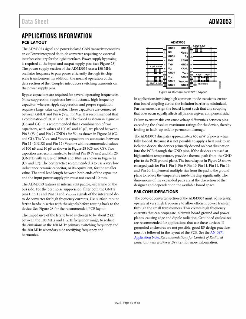
APPLICATIONS INFORMATION PCB LAYOUT The ADM3053 signal and power isolated CAN transceiver contains an isoPower integrated dc-to-dc converter, requiring no external interface circuitry for the logic interfaces. Power supply bypassing is required at the input and output supply pins (see Figure 28). The power supply section of the ADM3053 uses a 180 MHz oscillator frequency to pass power efficiently through its chip-scale transformers. In addition, the normal operation of the data section of the iCoupler introduces switching transients on the power supply pins.
Bypass capacitors are required for several operating frequencies. Noise suppression requires a low inductance, high frequency capacitor, whereas ripple suppression and proper regulation require a large value capacitor. These capacitors are connected between GND1 and Pin 6 (VIO) for VIO. It is recommended that a combination of 100 nF and 10 nF be placed as shown in Figure 28 (C6 and C4). It is recommended that a combination of two capacitors, with values of 100 nF and 10 µF, are placed between Pin 8 (VCC) and Pin 9 (GND1) for VCC as shown in Figure 28 (C2 and C1). The VISOIN and VISOOUT capacitors are connected between Pin 11 (GND2) and Pin 12 (VISOOUT) with recommended values of 100 nF and 10 µF as shown in Figure 28 (C5 and C8). Two capacitors are recommended to be fitted Pin 19 (VISOIN) and Pin 20 (GND2) with values of 100nF and 10nF as shown in Figure 28 (C9 and C7). The best practice recommended is to use a very low inductance ceramic capacitor, or its equivalent, for the smaller value. The total lead length between both ends of the capacitor and the input power supply pin must not exceed 10 mm.
The ADM3053 features an internal split paddle, lead frame on the bus side. For the best noise suppression, filter both the GND2 pins (Pin 11 and Pin13) and VISOOUT signals of the integrated dc-to-dc converter for high frequency currents. Use surface-mount ferrite beads in series with the signals before routing back to the device. See Figure 28 for the recommended PCB layout.
The impedance of the ferrite bead is chosen to be about 2 kΩ between the 100 MHz and 1 GHz frequency range, to reduce the emissions at the 180 MHz primary switching frequency and the 360 MHz secondary side rectifying frequency and harmonics.
0929
3-02
8
GND11
NC2
GND13
RxD4
GND2 20
VISOIN 19
RS 18
CANH 17
TxD5 GND2 16
VIO6 CANL 15
GND17 VREF 14
VCC8 GND2 13
GND19 VISOOUT 12
GND110 GND2 11
ADM30530.01µF 0.1µF
0.1µF 10µF
0.1µF 0.01µF
10µF 0.1µF FERRITES
Figure 28. Recommended PCB Layout
In applications involving high common-mode transients, ensure that board coupling across the isolation barrier is minimized. Furthermore, design the board layout such that any coupling that does occur equally affects all pins on a given component side.
Failure to ensure this can cause voltage differentials between pins exceeding the absolute maximum ratings for the device, thereby leading to latch-up and/or permanent damage.
The ADM3053 dissipates approximately 650 mW of power when fully loaded. Because it is not possible to apply a heat sink to an isolation device, the devices primarily depend on heat dissipation into the PCB through the GND pins. If the devices are used at high ambient temperatures, provide a thermal path from the GND pins to the PCB ground plane. The board layout in Figure 28 shows enlarged pads for Pin 1, Pin 3, Pin 9, Pin 10, Pin 11, Pin 14, Pin 16, and Pin 20. Implement multiple vias from the pad to the ground plane to reduce the temperature inside the chip significantly. The dimensions of the expanded pads are at the discretion of the designer and dependent on the available board space.
EMI CONSIDERATIONS The dc-to-dc converter section of the ADM3053 must, of necessity, operate at very high frequency to allow efficient power transfer through the small transformers. This creates high frequency currents that can propagate in circuit board ground and power planes, causing edge and dipole radiation. Grounded enclosures are recommended for applications that use these devices. If grounded enclosures are not possible, good RF design practices must be followed in the layout of the PCB. See the AN-0971 Application Note, Recommendations for Control of Radiated Emissions with isoPower Devices, for more information.
ADM3053 Data Sheet
Rev. E | Page 16 of 18
RS PIN For high speed mode, the RS pin is connected directly to GND2 (Pin 16 or Pin 20). The transition time of the CAN bus signals are short as possible, allowing higher speed signaling. A shielded cable is recommended to avoid EMI problems in high speed mode.
Slope control mode allows the use of unshielded twisted pair wires or parallel pair wires as bus lines. The signal rise and fall transition times are slowed to reduce EMI and ringing. The rise and fall slopes are adjusted with the resistor (RSLOPE) connected from RS to GND2. See Figure 6 for details.
The RS pin cannot be left floating.
INSULATION LIFETIME All insulation structures eventually break down when subjected to voltage stress over a sufficiently long period. The rate of insulation degradation is dependent on the characteristics of the voltage waveform applied across the insulation. Analog Devices conducts an extensive set of evaluations to determine the lifetime of the insulation structure within the ADM3053.
Accelerated life testing is performed using voltage levels higher than the rated continuous working voltage. Acceleration factors for several operating conditions are determined, allowing calculation of the time to failure at the working voltage of interest. The values shown in Table 5 summarize the peak voltages for 50 years of service life in several operating conditions. In many cases, the working voltage approved by agency testing is higher than the 50 year service life voltage. Operation at working voltages higher than the service life voltage listed leads to premature insulation failure.
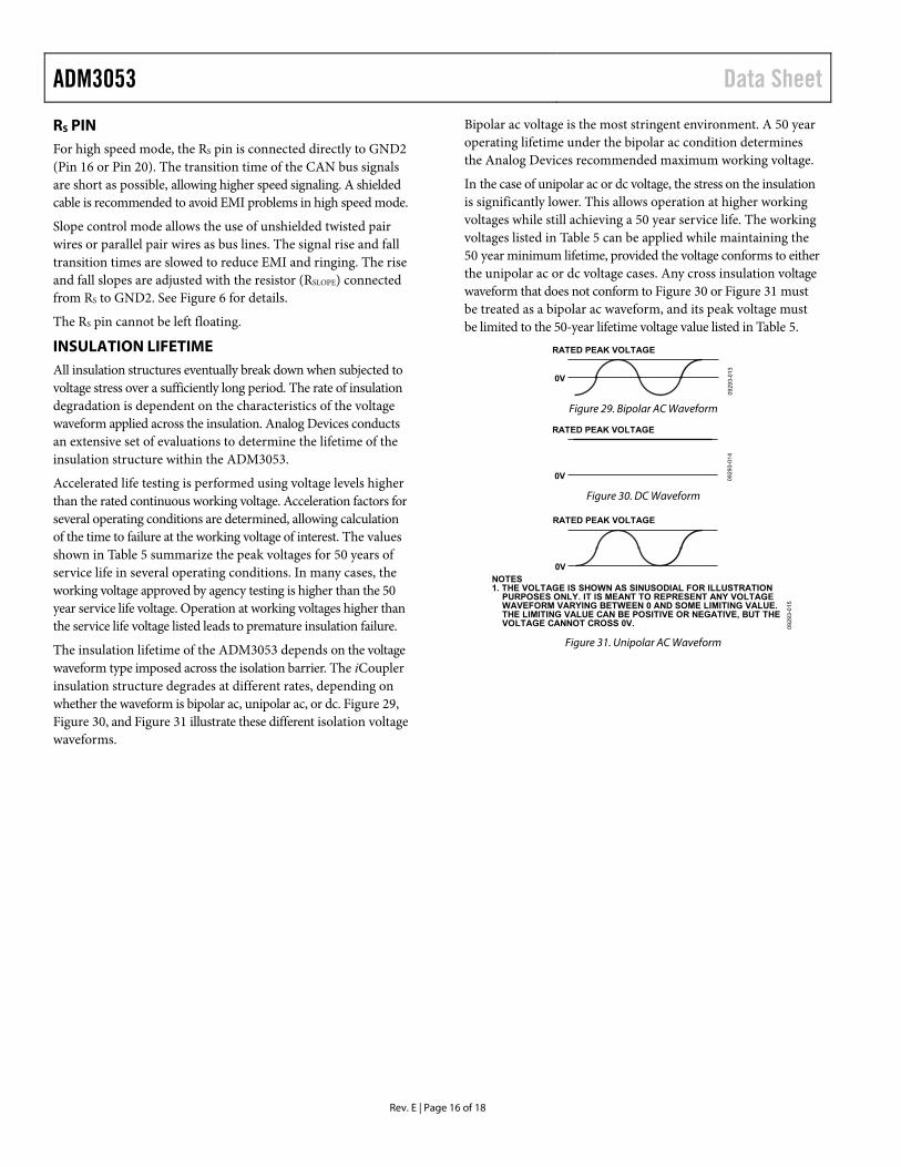
The insulation lifetime of the ADM3053 depends on the voltage waveform type imposed across the isolation barrier. The iCoupler insulation structure degrades at different rates, depending on whether the waveform is bipolar ac, unipolar ac, or dc. Figure 29, Figure 30, and Figure 31 illustrate these different isolation voltage waveforms.
Bipolar ac voltage is the most stringent environment. A 50 year operating lifetime under the bipolar ac condition determines the Analog Devices recommended maximum working voltage.
In the case of unipolar ac or dc voltage, the stress on the insulation is significantly lower. This allows operation at higher working voltages while still achieving a 50 year service life. The working voltages listed in Table 5 can be applied while maintaining the 50 year minimum lifetime, provided the voltage conforms to either the unipolar ac or dc voltage cases. Any cross insulation voltage waveform that does not conform to Figure 30 or Figure 31 must be treated as a bipolar ac waveform, and its peak voltage must be limited to the 50-year lifetime voltage value listed in Table 5.
0V
RATED PEAK VOLTAGE
0929
3-01
3
Figure 29. Bipolar AC Waveform
0V
RATED PEAK VOLTAGE
0929
3-01
4
Figure 30. DC Waveform
0V
RATED PEAK VOLTAGE
NOTES1. THE VOLTAGE IS SHOWN AS SINUSODIAL FOR ILLUSTRATION PURPOSES ONLY. IT IS MEANT TO REPRESENT ANY VOLTAGE WAVEFORM VARYING BETWEEN 0 AND SOME LIMITING VALUE. THE LIMITING VALUE CAN BE POSITIVE OR NEGATIVE, BUT THE VOLTAGE CANNOT CROSS 0V. 09
293-
015
Figure 31. Unipolar AC Waveform
Data Sheet ADM3053
Rev. E | Page 17 of 18
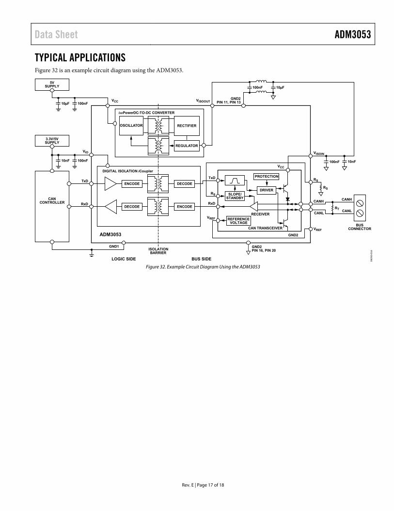
TYPICAL APPLICATIONS Figure 32 is an example circuit diagram using the ADM3053.
CANCONTROLLER
3.3V/5VSUPPLY
100nF10nF 100nF 10nF
CANH
CANLRT
BUSCONNECTOR
5VSUPPLY
100nF10µF
10µF100nF
RS
ADM3053
TxD
RxD
ISOLATIONBARRIER
GND1
LOGIC SIDE BUS SIDE
ENCODE
DECODE
DECODE
ENCODE
OSCILLATOR RECTIFIER
REGULATOR
VISOOUT
DIGITAL ISOLATION iCoupler
isoPowerDC-TO-DC CONVERTER
GND2PIN 11, PIN 13
VIO VISOIN
RS
CANH
CANL
VREF
REFERENCEVOLTAGE
RECEIVER
CAN TRANSCEIVER
TxD
RS
RxD
VREF
GND2
VCC
SLOPE/STANDBY
DRIVER
PROTECTION
VCC
09
29
3-0
16
GND2PIN 16, PIN 20
Figure 32. Example Circuit Diagram Using the ADM3053

ADM3053 Data Sheet
Rev. E | Page 18 of 18
OUTLINE DIMENSIONS
CONTROLLING DIMENSIONS ARE IN MILLIMETERS; INCH DIMENSIONS(IN PARENTHESES) ARE ROUNDED-OFF MILLIMETER EQUIVALENTS FORREFERENCE ONLY AND ARE NOT APPROPRIATE FOR USE IN DESIGN.
COMPLIANT TO JEDEC STANDARDS MS-013-AC
13.00 (0.5118)12.60 (0.4961)
0.30 (0.0118)0.10 (0.0039)
2.65 (0.1043)2.35 (0.0925)
10.65 (0.4193)10.00 (0.3937)
7.60 (0.2992)7.40 (0.2913)
0.75 (0.0295)0.25 (0.0098) 45°
1.27 (0.0500)0.40 (0.0157)
COPLANARITY0.10 0.33 (0.0130)
0.20 (0.0079)0.51 (0.0201)0.31 (0.0122)
SEATINGPLANE
8°0°
20 11
101
1.27(0.0500)
BSC
06-0
7-20
06-A
Figure 33. 20-Lead Standard Small Outline Package [SOIC_W]
Wide Body (RW-20)
Dimensions shown in millimeters and (inches)
ORDERING GUIDE
Model1 Temperature Range Package Description Package Option
ADM3053BRWZ −40°C to +85°C 20-Lead Standard Small Outline Package [SOIC_W] RW-20 ADM3053BRWZ-REEL7 −40°C to +85°C 20-Lead Standard Small Outline Package [SOIC_W] RW-20 EVAL-ADM3053EBZ Evaluation Board EZLINX-IIIDE-EBZ iCoupler Isolated Interface Development Environment Evaluation Board 1 Z = RoHS Compliant Part.
©2011–2017 Analog Devices, Inc. All rights reserved. Trademarks and registered trademarks are the property of their respective owners. D09293-0-12/17(E)